Title Experimental study on fracture characteristics of ...
101
RIGHT: URL: CITATION: AUTHOR(S): ISSUE DATE: TITLE: Experimental study on fracture characteristics of graphene for development of transparent electrode( Dissertation_全文 ) Jang, Bongkyun Jang, Bongkyun. Experimental study on fracture characteristics of graphene for development of transparent electrode. 京都大学, 2017, 博士(工学) 2017-09-25 https://doi.org/10.14989/doctor.k20700 許諾条件により本文は2018-09-24に公開
Transcript of Title Experimental study on fracture characteristics of ...
RIGHT:
URL:
CITATION:
AUTHOR(S):
ISSUE DATE:
TITLE:
Experimental study on fracturecharacteristics of graphene for developmentof transparent electrode( Dissertation_全文 )
Jang, Bongkyun
Jang, Bongkyun. Experimental study on fracture characteristics of graphene fordevelopment of transparent electrode. 京都大学, 2017, 博士(工学)
2017-09-25
https://doi.org/10.14989/doctor.k20700
許諾条件により本文は2018-09-24に公開

Experimental study on
fracture characteristics of graphene
for development of transparent electrode
September, 2017
Bongkyun Jang

i
Contents
Chapter 1 Introduction 1
1.1 Graphene………………………………………………...…………... 1
1.2 Mechanical and fracture behavior of graphene……………………… 2
1.3 Applications of graphene using superior mechanical properties……. 3
1.4 Overview of this thesis………………………………………………. 4
Chapter 2 Development of fracture testing method for graphene 9
2.1 Introduction…………………………………………………………… 9
2.2 Experimental………..……………………………………………….... 11
2.2.1 Specimen fabrication………………………..………………… 11
2.2.2 In situ fracture mechanics tests under uniaxial tension………... 15
2.3 Results and discussions 19
2.4 Conclusion……………………………………………………………. 27
Chapter 3 Fracture characteristics of multilayer graphene 33
3.1 Introduction…………………………………………………………… 33
3.2 Experimental……….…………………………………………………. 35
3.2.1 Specimen fabrication……………………. 35
3.2.2 Precrack machining 36
3.2.3 In situ mode I fracture test 37

CONTENTS ii
3.3 Results and discussions…………………………………… 38
3.3.1 Fracture toughness of multilayer graphene…………………. 38
3.3.2 Nonlinear elastic fracture mechanics.. 42
3.3.3 Asynchronous crack propagation with dissimilar paths in
multilayer graphene
44
3.4 Conclusion……………………………………………………………. 49
Chapter 4 Reduction of fracture damage on graphene in transfer
process for transparent electrode
53
4.1 Introduction…………………………………………………………… 53
4.2 Experiments and results..……………………………………………… 55
4.2.1 Fabrication process of graphene transparent
electrode………....……………………………………………
55
4.2.2 Dependence of contact pressure on electrical properties…..….. 59
4.2.3 Failure modes in transfer process of graphene……………..…. 62
4.2.4 Numerical simulation…...…………………………………….. 68
4.2.5 Large area transfer of graphene 71
4.3 Conclusion…………………………………………………………….. 73
Appendix A 79
Appendix B 83
Chapter 5 Conclusion 87
List of publications 91
Acknowledgements 95
1
Chapter 1
Introduction
1.1 Graphene
Graphene is a two dimensional material which has attracted the interests of scientists
and engineers in various area for a decade, since it can be easily isolated from natural
graphite with mechanical exfoliation by Andre Geim and Konstantin Novoselov [1]. It
has a hexagonal honeycomb structure composed of carbon atoms with sp2 bonding like
carbon nanotube and fullerene. Since the sp2-hybrided carbon atoms are arranged in single
plane, graphene is the thinnest known material with only a single atom thick, which makes
it difficult to define the thickness of single atomic layer graphene. Most of researches
regards the thickness of monolayer graphene as the interlayer distance of graphite; 0.335
nm [2,3,4]. Multilayer graphene including bilayer graphene and trilayer graphene is
composed of monolayer graphenes bound with π electron interaction and van der Waals
interaction among the layers [5,6,7].
Graphene has an outstanding physical properties. Its exceptional electrical properties
such as high electron mobility and quantum Hall effect at room temperature have
stimulated a lot of researches on the applications to the electronic devices [1]. The
reported electron mobility is more than 200,000 cm2⋅V-1⋅s-1, which is measured for
2 CHAPTER 1 INTRODUCTION
suspended graphene [8]. By mechanical cleavage technique, quantum Hall effect,
predicted by several physicians, was confirmed experimentally by Geim’s group and
Kim’s group [9,10]. Monolayer graphene is optically transparent, and absorb only 2.3%
of visual light due to its atomically thin crystal structure [11]. Hence, the number of
graphene layers can be identified by the transmittance in multilayer graphene [12].
Thermal conductivity of graphene is up to 5300 W⋅m-1⋅K-1, which is three times higher
that of pyrolytic graphite at room temperature [13,14].
There are several methods for the fabrication of graphene. Although a lot of
fabrication methods of graphene have been developed until now, the appropriate methods
should be used according to its applications. Mechanically exfoliated graphene from
natural graphite or highly oriented pyrolytic graphite (HOPG) has high purity and low
defects, so it is called pristine graphene [1]. However, it takes a lot of time and efforts to
fabricate graphene and its maximum size is limited with conventional exfoliation
technique. Therefore this method is mainly used in fundamental researches of graphene.
Chemical vapor deposition (CVD) process has advantages of scalability, high coverage,
and cost efficiency. Using methane precursor and copper foil as a catalyst, meter scale
graphene can be synthesized and transferred on various substrate for the application of
graphene. CVD-grown graphene is polycrystalline and its optical transparency and
electrical conductivity are used for the various applications. Third is chemical reduction
method. Monolayer graphene flake can be produced by the chemical reduction of
graphene oxide. This method is the inexpensive method. However graphene obtained by
this process has low quality and a lot of defects due to imperfect removals of functional
groups and damages during the reduction process. Lastly, epitaxial growth of graphene
on silicon carbide substrate has a merit of the wafer scale process. However it is not
widely used due to high cost of the substrate.
1.2 Mechanical and fracture behavior of graphene
The mechanical behavior of graphene has been studied mainly analytical methods
since it is easy to approach due to its similarities with carbon nanotubes and graphite. Liu
et al. calculated the mechanical behavior of graphene under uniaxial tension [15].

1.2 MECHANICAL PROPERTIES AND FRACTURE BEHAVIOR OF
GRAPHENE 3
According to their density function theory simulation, the Young’s modulus is 1.05 TPa
and the intrinsic strength is 110 GPa for a zigzag direction, and 121 GPa for an armchair
direction. On the other hand, there are a few experimental results, since it is difficult to
handle atomically thin layers, and to measure the force applied to the graphene. For
pristine monolayer graphene exfoliated from graphite, Lee et al. reported the Young’s
modulus of 1.0 TPa, the intrinsic strength and strain of 130 GPa and 0.25, which is the
strongest materials ever tested [2]. They measured the mechanical properties by an
indentation of the monolayer graphene suspended on circular hole with atomic force
microscopy. For the fracture characteristics of graphene, Omeltchenko et al. obtained 4.7
MPa√m of fracture toughness by molecular dynamics simulation [16]. Experimental
researches started from polycrystalline graphene fabricated by CVD process. Hwangbo
et al. bulged polycrystalline graphene membrane on circular hole, and measured fracture
toughness of monolayer graphene by applying pressure to the membrane [17]. Their result
was 10.7 MPa√m, which is about two times larger than estimated value by the simulation.
Zhang, et al. reported fracture toughness of bilayer CVD-graphene with pre-cracked with
focused ion beam [18]. With MEMS tensile devices, they performed in situ uniaxial
tensile test in a scanning electron microscope (SEM), and obtained 4.0 MPa√m of
fracture toughness. Also, chemically-synthesized multilayer graphene with a single
crystal structure was tested by Wei, et al. and, 12.0 MPa√m is reported as fracture
toughness [19]. In situ tensile test is carried out with 10 layers of notched graphene
obtained from flattened nanotubes in a transmission electron microscope (TEM). Several
test results of a fracture toughness of graphene shows large deviation of results due to
difficulties of experiments and preparation of the specimen.
1.3 Applications of graphene using superior mechanical properties
With these extraordinary physical properties, uncountable potential applications for
electronics, biology, energy harvesting and storage, sensor, lightweight high-performance
composite materials, lubricant, heat emission material etc. are developed [20]. Among
them, exceptional mechanical properties extend the unprecedented applications of
graphene.

4 CHAPTER 1 INTRODUCTION
Firstly, the most prospective application is flexible electronics due to its large failure
strain. To be specific, flexible transparent electrodes fabricated with graphene reached
close to the commercialization recently [20,21,22]. Especially, it is expected that they can
replace the transparent electrode with conventional brittle materials like indium tin oxide
[23]. Graphene synthesized by CVD process is transferred on transparent polymer
substrate with roll-to-roll process for the scalable manufacture [21]. Since graphene is
synthesized on copper foil by CVD process, it should be transferred on polyethylene
terephthalate (PET) film for the flexible transparent electrode. In the transfer process,
graphene experiences various modes of stress due to mechanical contacts between the
surfaces laminated films. Hence, various sizes of cracks or holes are observed after
transferring on target substrates [24]. Hence it is necessary to eliminate these mechanical
damages during the fabrication process. Moreover, flexible electronic devices can deform
mechanically during the operation of bending, stretching, and twisting. These strains will
make cracks so that the performance of the devices will be degraded [25]. Therefore,
mechanical behavior of graphene should be fully understood to design the graphene-
based devices and the fabrication process.
Another promising application using superior mechanical properties of graphene is
graphene composite materials, which are expected to obtain higher strength and
toughness than conventional carbon based materials or to possess additional physical
properties such as high electrical conductivity and thermal conductivity [26,27,28,29].
Since graphene is two-dimensional materials, its surface area can be maximized when it
is well-dispersed in the polymer matrix. To develop and design graphene-based composite
materials, it is essential to understand the mechanical properties of individual components
such as graphene and polymer matrix, as well as interaction of these components [30].
Electromechanical applications have also studied in the area of micro
electromechanical system. High elastic modulus and large surface area per unit mass of
graphene make it possible to utilize it as nano mechanical resonator for mass sensing with
high resolution [31]. The application mechanical sensors can contribute the development
of mobile devices and IoT (Internet of Things) devices in near future.
1.2 MECHANICAL PROPERTIES AND FRACTURE BEHAVIOR OF
GRAPHENE 5
1.4 Overview of this thesis
In this dissertation, fracture characteristics of graphene using in situ mode I fracture
test under SEM are investigated, and the improved transfer process to mitigate fracture
damages of graphene for the application of transparent conductive electrode is proposed.
The thesis is organized as follows.
In chapter 2, uniaxial fracture testing method of pristine graphene is developed.
Freestanding graphene fracture testing specimen with micro scale is fabricated with novel
transfer method. In situ uniaxial tensile test is performed under SEM to monitor the
fracture behavior of graphene. The results of the experiments are analyzed with finite
element method (FEM) to obtain the mechanical properties and fracture toughness of
graphene. Finally, the accurate fracture testing method of graphene is discussed.
In chapter 3, fracture characteristics of multilayer graphene is investigated. Mode I
graphene fracture testing specimen with single edge crack is fabricated established
method in chapter 2. From the in situ fracture test, fracture toughness of multilayer
graphene is evaluated using the experimental results and FEM calculation. Nonlinear
fracture characteristics of multilayer graphene is discussed under the consideration of
nonlinear constitutive equations and large deformation. Finally, unique crack
propagations, which is asynchronous cracking with dissimilar paths in multilayer
graphene observed in in situ SEM images, are discussed and explained the mechanisms
of these phenomena.
In chapter 4, the methods to reduce fracture damage in the fabrication process of
graphene transparent electrode, are suggested. For the large-area fabrication of graphene
transparent electrode, graphene is transferred on a polymer substrate using roll-to-roll
transfer process. The contact pressure induced by nip rolls is attributed to the fracture
damages of graphene. From the observation of transferred graphene using SEM and the
FEM calculations, we categorized the failure modes of the transferred graphene, and
suggested the damage reduction method of graphene during the transfer process.
In chapter 5, the obtained results in this thesis are summarized and discussed.
6 CHAPTER 1 INTRODUCTION
References
[1] K.S. Novoselov, A.K. Geim, S.V. Morozov, D. Jiang, Y. Zhang, S.V. Dubonos, I.V.
Grigorieva, A.A. Firsov, Electric field effect in atomically thin carbon films. Science
306 (2004) 666-669.
[2] C. Lee, X. Wei, J.W. Kysar, J. Hone, Measurement of the elastic properties and
intrinsic strength of monolayer graphene. Science 321 (2008) 385-388.
[3] R. Al-Jishi, G. Dresselhaus, Lattice-dynamical model for graphite. Phys. Rev. B 26
(1982) 4514-4522.
[4] B.T. Kelly, Physics of graphite. (Applied Science, London, 1982)
[5] X. Wei, Z. Meng, L. Ruiz, X. Xia, C. Lee, J.W. Kysar, J.C. Hone, S. Keten, H.D.
Espinosa, Recoverable slippage mechanism in multilayer graphene leads to
repeatable energy dissipation, ACS Nano 10 (2016) 1820–1828.
[6] G.S. Verhoeven, M. Dienwiebel, J.W.M. Frenken, Model calculations of
superlubricity of graphite, Phys. Rev. B 70 (2004) 165418.
[7] X. Feng, S. Kwon, J.Y. Park, M. Salmeron, Superlubric sliding of graphene
nanoflakes on graphene, ACS Nano 7 (2013) 1718-1724.
[8] K.I. Bolotin, K.J. Sikes, Z. Jiang, M. Klima, g. Fudenberg, J. Hone, P. Kim, H.L.
Stomer, Ultra electron mobility in suspended graphene, Solid State Commun. 146
(2008) 351-355.
[9] K.S. Novoselov, A.K. Geim, S.V. Morozov, D. Jiang, M.I. Katsnelson, I.V.
Grigorieva, S.V. Dubonos, A.A. Firsov, Two-dimensional gas of massless Dirac
fermions in graphene, Nature 438 (2005) 197-200.

REFERENCES 7
[10] Y. Zhang, Y.-W. Tan, H.L. Stormer, P. Kim, Experimental observation of the
quantum Hall effect and Berry’s phase in graphene, Nature 438 (2005) 201-204.
[11] R.R. Nair, P. Blake, A.N. Grigorenko, K.S. Novoselov, T.J. Booth, T. Stauber,
N.M.R. Peres, A.K. Geim, Fine structure constant defines visual transparency of
graphene, Science 320 (2008) 1308.
[12] H.S. Skulason, P.E. Gaskell, T. Szkopek, Optical reflection and transmission
properties of exfoliated graphite from a graphene monolayer to several hundred
graphene layers, Nanotechnology 21 (2010) 295709.
[13] A.A. Blandin, S. Ghosh, W. Bao, I. Calizo, D. Teweldebrhan, F. Miao, C.N. Lau,
Superior thermal conductivity of single-layer graphene, Nano Lett. 8 (2008) 902-907.
[14] G.A. Slack, Anisotropic thermal conductivity of pyrolytic graphite, Phys. Rev. 127
(1962) 694-696.
[15] F. Liu, P. Ming, J. Li, Ab initio calculation of ideal strength and phonon instability
of graphene under tension, Phys. Rev. B 76 (2007) 054120.
[16] A. Omeltchenko, J. Yu, R.K. Kalia, P. Vashishta, Crack front propagation and
fracture in a graphite sheet: A molecular-dynamics study on parallel computers, Phys.
Rev. Lett. 78 (1997) 2148-2151.
[17] Y. Hwangbo, C.-K. Lee, S.-M. Kim, J.-H. Kim, K.-S. Kim, B. Jang, H.-J. Lee, S.-K.
Lee, S.-S. Kim, J.-H. Ahn, S.-M. Lee, Fracture characteristics of monolayer CVD-
graphene. Sci. Rep. 4 (2014) 4439.
[18] P. Zhang, L. Ma, F. Fan, Z. Zeng, C. Peng, P.E. Loya, Z. Liu, Y. Gong, J. Zhang, X.
Zhang, P.M. Ajayan, T. Zhu, J. Lou, Fracture toughness of graphene, Nat. Commun.
5 (2014) 3782.
[19] X. Wei, S. Xiao, F. Li, D.-M. Tang, Q. Chen, Y. Bando, D. Golberg, Comparative
fracture toughness of multilayer graphenes and boronitrenses, Nano. Lett. 15 (2015)
689-694.
[20] A. Zurutuza, C. Marinelli, Challenges and opportunities in graphene
commercialization, Nature Nanotech. 9 (2014) 730-734.
[21] S. Bae, H. Kim, Y. Lee, X. Xu, J.-S. Park, Y. Zheng, J. Balakrishnan, T. Lei, H.R.
Kim, Y.I. Song, Y.-J. Kim, K.S. Kim, B. Ö zyilmaz, J.-H. Ahn, B.H. Hong, S. Iijima,
8 CHAPTER 1 INTRODUCTION
Roll-to-roll production of 30-inch graphene films for transparent electrodes, Nat.
Nanotechnol. 5 (2010) 574–578.
[22] J. Ryu, Y. Kim, D. Won, N. Kim, J.S. Park, E.-K. Lee, D. Cho, S.-P. Cho, S.J. Kim,
G.H. Ryu, H.-A.-S. Shin, Z. Lee, B.H. Hong, S. Cho, Fast synthesis of high-
performance graphene films by hydrogen-free rapid thermal chemical vapor
deposition, ACS Nano 8 (2014) 950–956.
[23] L.G. De Arco, Y. Zhang, C.W. Schlenker, K. Ryu, M.E. Thompson, C. Zhou,
Continuous, highly flexible, and transparent graphene films by chemical vapor
deposition for orgainc photovoltaics, ACS Nano 4 (2010) 2865-2873.
[24] J. Kang, S. Hwang, J.H. Kim, M.H. Kim, J. Ryu, S.J. Seo, B.H. Hong, M.K. Kim,
J.-B. Choi, Efficient transfer of large-area graphene films onto rigid substrates by hot
pressing, ACS Nano 6 (2012) 5591–5598.
[25] S. Won, Y. Hwango, S.-K. Lee, K.-S. Kim, K.-S. Kim, S.-M. Lee, H.-J. Lee, J.-H.
Ahn, J.-H. Kim, S.-B. Lee, Double-layer CVD graphene as stretchable transparent
electrodes, Nanoscale 6 (2014) 6057-6064.
[26] S. Stankovich, D.A. Dikin, G.H.B. Dommett, K.M. Kohlhaas, E.J. Zimney, E.A.
Stach, R.D. Piner, S.T. Nguyen, R.S. Ruoff, Graphene-based composite materials,
Nature 442 (2006) 282–286.
[27] R. Atif, I. Shyha, F. Inam, Mechanical, thermal, and electrical properties of
graphene-epoxy nanocomposites-a review, Polymers 8 (2016) 281.
[28] H.D. Espinosa, A.L. Juster, F.J. Latourte, O.Y. Loh, D. Gregoire, P.D. Zavattieri,
Tablet-level origin of toughening in abalone shells and translation to synthetic
composite materials, Nat. Commun. 2 (2011) 173.
[29] X. Sun, H. Sun, H. Li, H. Peng, Developing polymer composite materials: carbon
nanotubes or graphene? Adv. Mater. 25 (2013) 5153-5176.
[30] S. Chandrasekaran, N. Sato, F. Tölle, R. Mülhaupt, B. Fiedler, Fracture toughness
and failure mechanism of graphene based epoxy composites, Compos. Sci. Technol.
97 (2014) 90–99.
[31] J.S. Bunch, A.M. van der Zande, S.S. Verbridge, I.W. Franck, D.M. Tanenbaum,
J.M. Parpia, H.G. Craighead, P.L. McEuen, Electromechanical resonators from
graphene sheets, Science 26 (2007) 490-493.

9
Chapter 2
Development of fracture testing method
for graphene
2.1 Introduction
Graphene, a carbon material with sp2-bonding (e.g., fullerenes, carbon nanotubes, and
graphite) has outstanding physical properties. The pioneering research on graphene was
performed on the electrical characteristics of single-layer graphene exfoliated from
graphite by micromechanical cleavage, the so-called “Scotch tape” technique [1]. The
pristine graphene with perfect crystallinity can be obtained in this way, and has been
extensively investigated in terms of its electrical, optical, chemical, and mechanical
properties [1–4]. Based on the extraordinary physical properties of graphene, numerous
potential applications have been studied, developed, and commercialized [5].
The outstanding mechanical properties of graphene have been highlighted as
particularly promising for future nanomaterial applications. To date, various graphene-
based flexible and stretchable electronic devices such as transistors, light-emitting diodes,
energy harvesters, energy storage devices, and sensors have been demonstrated by
utilizing its ultra-high strength over 100 GPa and failure strain over 25% together with its
electrical and optical conductivities [6–10]. The mechanical properties of graphene have
been also exploited in high-performance lightweight composites, superelastic auxetic
metamaterials, and the thinnest lubricants [11–13]. The mechanical characteristics of
10 CHAPTER 2 DEVELOPMENT OF FRACTURE TESTING METHOD
graphene have stimulated development of new graphene applications.
Flexible electronic devices of graphene experience bending, stretching, and twisting
during their operations. These deformations can cause mechanical cracking to the
graphene layer in the devices, such that the performance of the devices degrades over
time [14]. Moreover, graphene can be easily fractured during the fabrication processes of
such devices, due to its atomistic thinness [15]. In this regards, further research on the
fracture behaviors of graphene is required for the increase of fabrication yield and
reliability of the graphene-based devices.
The fracture behavior of graphene has been studied mainly with numerical methods
[16,17], but experimental reports are very rare. Most experimental data have been
obtained using nanoindentation for mechanically-exfoliated pristine and chemically-
synthesized graphene suspended on circular holes [3,18]. To investigate the fracture
characteristics of graphene, the fracture mechanics test under uniaxial tension is the most
fundamental step because the fracture mode is easily controllable by the position and
shape of pre-cracks in the specimen under a given external load. The nanoindentation
method, used in many studies on graphene is not suitable for the fracture mechanics test
due to its concentrated loading [19]. A few experimental studies have been carried out
using the uniaxial fracture test and the biaxial bulge test for chemically synthesized
graphene [20–22]. For mechanically-exfoliated pristine graphene, however, there is no
report on the fracture mechanics tests due to its tricky process of specimen preparation.
Nonetheless, the pristine graphene is an ideal specimen for the fracture mechanics test of
graphene because of its single crystallinity and defect-free nature [23,24].
The uniaxial fracture mechanics test for pristine graphene should be designed
considering these issues: First, a specimen for the fracture test should be readily
accessible to analytical techniques, such as scanning electron microscopy (SEM),
transmission electron microscopy (TEM), and Raman spectroscopy, to measure the
shapes, sizes, and layer numbers of the specimen. Second, the pre-crack introduced in the
specimen should have an appropriate shape and position to induce the singular stress field
near the crack tip. Third, the specimen with the pre-crack should be robust despite the
fragile nature of the pre-cracked graphene during the characterization and fracture tests.

2.2 EXPERIMENTAL 11
Finally, the fracture test should be compatible with an in situ observation technique
because of the accurate alignments between loading direction and specimen geometries,
and visualization of crack propagation behavior during fracture tests.
In this chapter, a fracture mechanics testing method to investigate the fracture
behavior of single-crystal pristine graphene considering the aforementioned requirements
was developed. Exploiting the advantages of in situ fracture tests, an abrupt crack
propagation behavior of bilayer single-crystalline graphene, and a crack bridging
behavior during the crack extension along its zig-zag direction was observed.
2.2 Experimental
2.2.1 Specimen fabrication
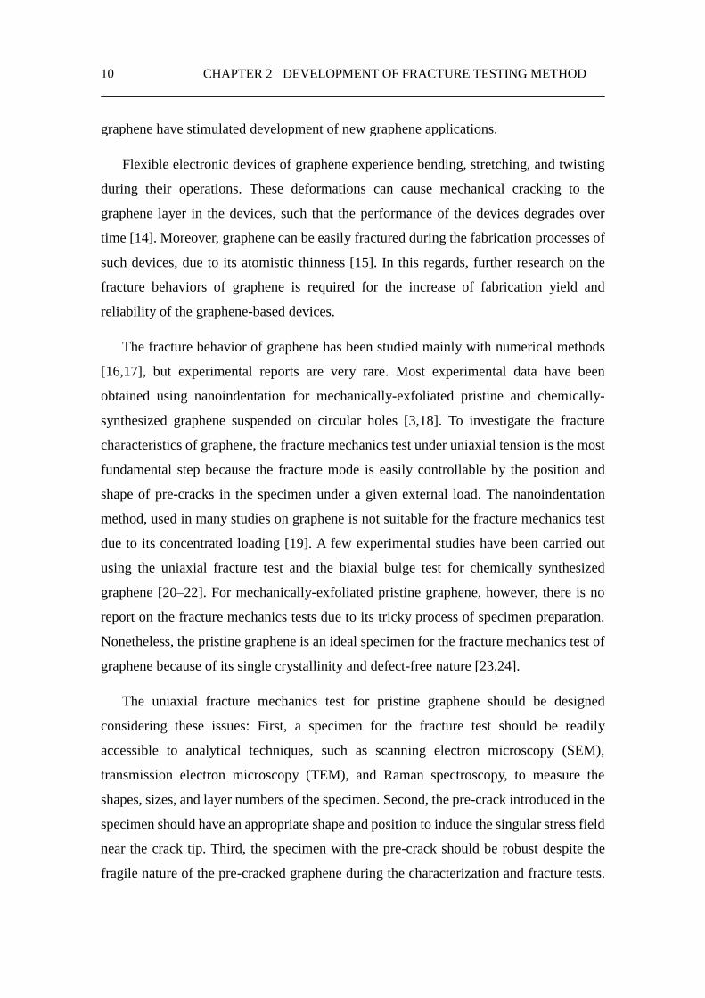
Procedures for fabricating a pristine graphene specimen for fracture mechanical
testing are illustrated in Figure 2.1. Pristine graphene was mechanically exfoliated from
graphite with Scotch tape and transferred to a silicon wafer with a silicon dioxide layer
(thickness: 400 nm), as shown in Figure 2.2(a) [1]. The layer numbers of graphene in the
dark strips in the image are identified from the optical contrast [4,25]. A strip of the
bilayer graphene was transferred onto a tensile device (Push to Pull Device, Hysitron). To
protect the graphene specimen during the transfer, it was spin-coated with poly(methyl
methacrylate) (PMMA), and the wafer with the coated specimen was etched out with 3%
potassium hydroxide (KOH) solution. Alignment in the tensile direction was adjusted
under an optical microscope (OM) with high magnification using micro-manipulators for
transferring the specimen onto the tensile device. For firm adhesion between the graphene
and the tensile device, the surface of the device was treated with oxygen plasma before
transferring, and annealed at 100°C in an oven after the transfer. The PMMA layer was
then removed by soaking gently in acetone, because surface tension of acetone can cause
damage to the suspended area of the specimen [26]. Figure 2.2(b), obtained from a high-
resolution scanning electron microscope (HR-SEM; S5500, Hitachi) shows the pristine
graphene specimen transferred on the tensile device. With a FIB (FB2200, Hitachi),
redundant graphene flakes and polymer residues on the tensile device were removed.
12 CHAPTER 2 DEVELOPMENT OF FRACTURE TESTING METHOD
Finally, both edges of the specimen were welded with tungsten to prohibit slippage
between the specimen and the tensile device by FIB deposition. In the fabrication, the
gallium ion beam used in FIB may damage the graphene around the fabrication area.
However, it is possible to minimize the lateral extent of any damage by reducing the
fabrication time [27].
A process to introduce a pre-crack in the graphene specimen is important for fracture
testing. The FIB was used for machining a narrow pre-crack with an accurate position
and dimensions. It is difficult to fabricate a pre-crack in an atomically thin layer, because
it can be easily broken due to the concentration of stress near the pre-crack tip during
fabrication. As mentioned above, it is important to pay attention to ion beam damage in
the fabrication by reducing the dose of the ion beam. The beam to perforate the graphene
is estimated to be in a range of 0.28 pA – 0.83 pA of beam current and 1 sec of exposure
time under a 30-kV acceleration voltage, which are sufficiently mild condition not to
damage the graphene. A minimum image scan was allowed for visualization of the
specimen to identify the accurate positioning and dimensions of the pre-crack. It is
important to also note that the beam should be exposed to the specimen under stabilized
conditions because beam drift can cause a blunt pre-crack tip.
2.2 EXPERIMENTAL 13
Figure 2.1. Specimen fabrication procedure. (a) Transfer and identification of the
graphene specimen. (b) Spin-coating of poly(methyl methacrylate) (PMMA). (c)
Separation of SiO2 wafer with KOH solution. (d) Transfer of the specimen onto a tensile
device with fine alignment under optical microscopy (OM) and removal of the PMMA.
(e) Focused ion beam (FIB) machining of a pre-crack for the fracture test. (f) Fracture test
under an applied tensile load.
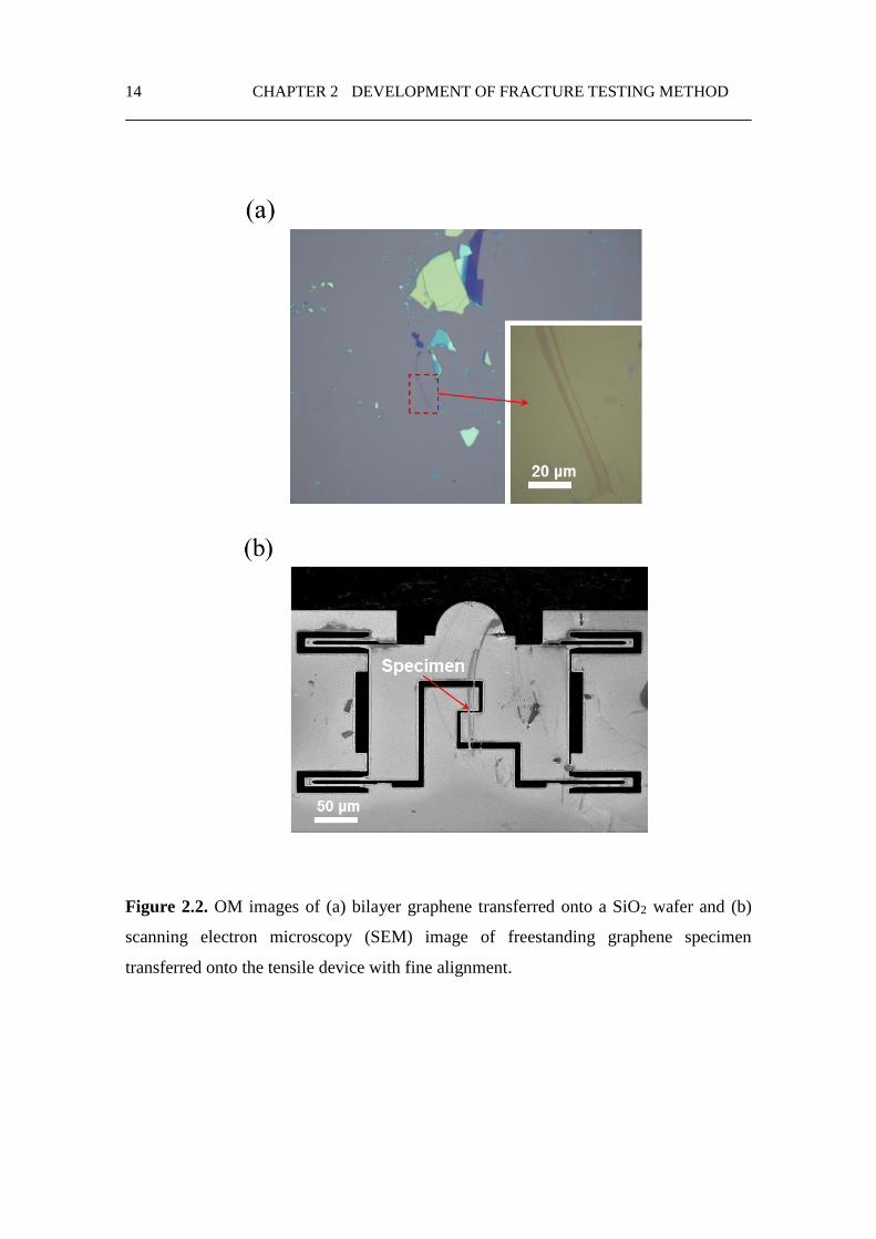
14 CHAPTER 2 DEVELOPMENT OF FRACTURE TESTING METHOD
Figure 2.2. OM images of (a) bilayer graphene transferred onto a SiO2 wafer and (b)
scanning electron microscopy (SEM) image of freestanding graphene specimen
transferred onto the tensile device with fine alignment.
2.2 EXPERIMENTAL 15
2.2.2 In situ fracture mechanics tests under uniaxial tension
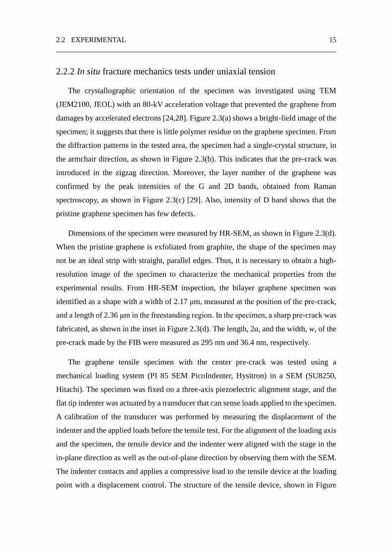
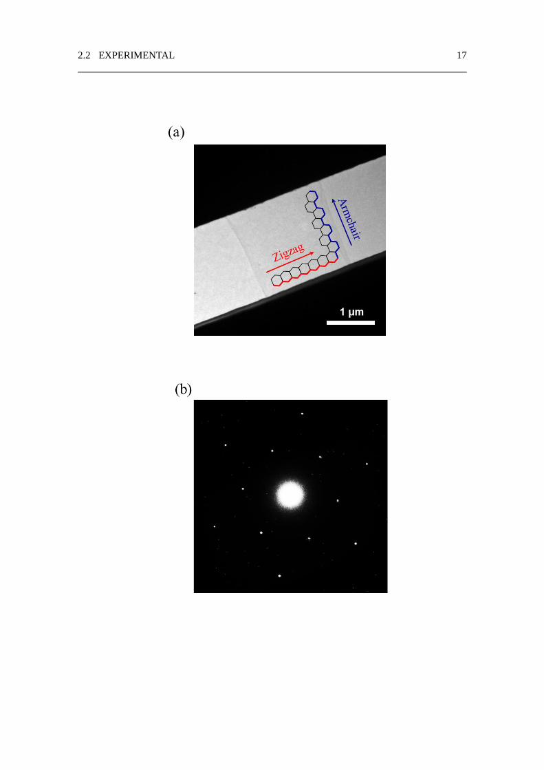
The crystallographic orientation of the specimen was investigated using TEM
(JEM2100, JEOL) with an 80-kV acceleration voltage that prevented the graphene from
damages by accelerated electrons [24,28]. Figure 2.3(a) shows a bright-field image of the
specimen; it suggests that there is little polymer residue on the graphene specimen. From
the diffraction patterns in the tested area, the specimen had a single-crystal structure, in
the armchair direction, as shown in Figure 2.3(b). This indicates that the pre-crack was
introduced in the zigzag direction. Moreover, the layer number of the graphene was
confirmed by the peak intensities of the G and 2D bands, obtained from Raman
spectroscopy, as shown in Figure 2.3(c) [29]. Also, intensity of D band shows that the
pristine graphene specimen has few defects.
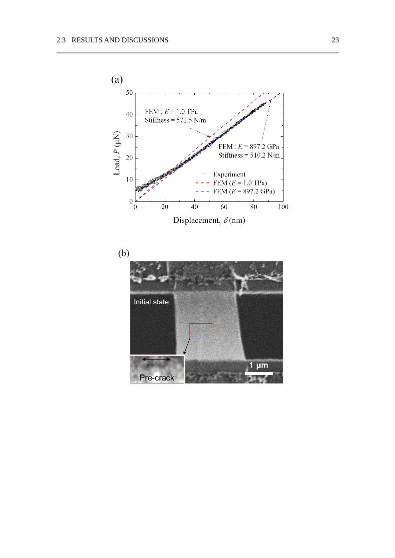
Dimensions of the specimen were measured by HR-SEM, as shown in Figure 2.3(d).
When the pristine graphene is exfoliated from graphite, the shape of the specimen may
not be an ideal strip with straight, parallel edges. Thus, it is necessary to obtain a high-
resolution image of the specimen to characterize the mechanical properties from the
experimental results. From HR-SEM inspection, the bilayer graphene specimen was
identified as a shape with a width of 2.17 μm, measured at the position of the pre-crack,
and a length of 2.36 μm in the freestanding region. In the specimen, a sharp pre-crack was
fabricated, as shown in the inset in Figure 2.3(d). The length, 2a, and the width, w, of the
pre-crack made by the FIB were measured as 295 nm and 36.4 nm, respectively.
The graphene tensile specimen with the center pre-crack was tested using a
mechanical loading system (PI 85 SEM PicoIndenter, Hysitron) in a SEM (SU8250,
Hitachi). The specimen was fixed on a three-axis piezoelectric alignment stage, and the
flat tip indenter was actuated by a transducer that can sense loads applied to the specimen.
A calibration of the transducer was performed by measuring the displacement of the
indenter and the applied loads before the tensile test. For the alignment of the loading axis
and the specimen, the tensile device and the indenter were aligned with the stage in the
in-plane direction as well as the out-of-plane direction by observing them with the SEM.
The indenter contacts and applies a compressive load to the tensile device at the loading
point with a displacement control. The structure of the tensile device, shown in Figure

16 CHAPTER 2 DEVELOPMENT OF FRACTURE TESTING METHOD
2.2(b), converts the compression into a tensile load in the specimen. The load detected by
the transducer is the sum of the loads applied to the specimen and the tensile device. To
extract the tensile load applied to the specimen, the stiffness of the tensile device is
calibrated using the stiffness of 207 N/m obtained by an additional loading after the tensile
experiments.
2.2 EXPERIMENTAL 17

18 CHAPTER 2 DEVELOPMENT OF FRACTURE TESTING METHOD
Figure 2.3. Inspection by transmission electron microscopy (TEM), Raman spectroscopy
and high-resolution SEM (HR-SEM). (a) Bright-field image obtained by TEM and (b)
diffraction pattern and (c) Raman spectrum of the graphene specimen, showing single
crystal and bilayer natures, respectively. (d) HR-SEM image of the graphene specimen in
which the pre-crack(inset) was machined with a FIB.
2.3 RESULTS AND DISCUSSIONS 19
2.3 Results and discussions
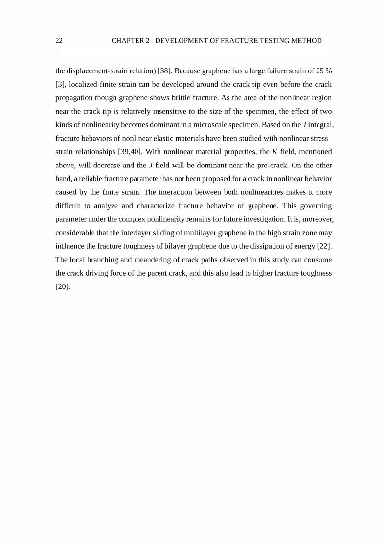
The load, 𝑃 and the displacement, 𝛿 curves are shown in Figure 2.4(a). Typically,
graphene suspended in a trench has residual stress because it tends to stick to the side
walls of the trench [3,20,26]. Thus, the initial part of the tensile loading graph shows a
low slope due to such residual stress. Apart from the initial loading region, the curve was
linear and the stiffness, 𝑘, was 510 N/m. The fracture load and displacement were 45.5
μN and 87.5 nm, respectively, and the load abruptly became zero after fracture. In
Figure 2.4(b) and (c), obtained by in situ SEM observation, the cracks started from the tip
of the pre-crack and propagated unstably along a zigzag direction to the edges of the
specimen at the moment of fracture. The fracture surface was straight and perpendicular
to the loading direction. From these results, bilayer graphene shows high stiffness and
brittle fracture behavior [3,21,22]. In Figure 2.4(d), I obtained the image of cracks by HR-
SEM after the fracture test to confirm crack propagation path of the graphene. Under
uniaxial tension, cracks tend to propagate perpendicular to the loading direction. Figure
2.4(c) and (d) indicate that the cracks globally propagate along with straight path
perpendicular to the loading direction, although the crack branching and the crack
meandering is locally observed. This result can be explained by the preferred crack
propagation of the zigzag crack from theoretical predictions under the loading of armchair
direction [30, 31]. The difference of the strength and the edge energy along the crystal
orientation is the main origin of this fracture behavior [16]. On the other hand, using the
developed methodology here, it is possible to perform the experiments with cracks
oriented different directions though the preparation of specimen requires further effort.
Assuming that the specimen is rectangular in shape and the width is 𝑊, the two-
dimensional stress can be defined as 𝜎2D = 𝑃/𝑛𝑊, where 𝑛 is the layer number of the
graphene. For the comparison of bulk materials, the three-dimensional stress can be
expressed as 𝜎3D = 𝑃/𝑡G𝑛𝑊. Here, the thickness of single-layer graphene is defined as
the average distance between layers of graphite, so 𝑡𝐺 = 0.335 nm. Then, two- and
three-dimensional Young’s moduli can be expressed as
20 CHAPTER 2 DEVELOPMENT OF FRACTURE TESTING METHOD
𝐸2D = 𝑘𝑙
𝑛𝑊 , 𝐸3D = 𝑘
𝑙
𝑡G𝑛𝑊. (1)
Here, 𝑙 is the initial length of the specimen. Assuming the specimen is rectangular in
shape, and adopting the representative width 𝑊 as 2.17 μm, the two- and three-
dimensional Young’s moduli are 𝐸2D = 273 N/m and 𝐸3D = 816 GPa, respectively.
However, as seen in Figure 2.3(d), the width of the specimen is not actually uniform and
the effect of the pre-crack should be considered. For a more accurate analysis, it is
necessary to construct a numerical model with an identical shape and dimensions as the
specimen and to calculate the stress distributions in the specimen by FE analysis. Using
the image obtained from the HR-SEM, specimen edges were defined with an edge
detection algorithm (LabVIEW Vision, National Instruments), and the model geometry
with the same shape of the actual specimen was constructed from the image processing,
as shown in Figure 2.5(a). The minimum mesh size near the pre-crack was about 0.03 nm,
and shell elements with a thickness of 0.67 nm were used for the simulation. The bottom
edge was clamped and the nodes of the top edge were assigned a uniform displacement
of 100 nm. Under the finite deformation conditions, FE analysis was carried out using
commercial FE software ABAQUS. Because both Young’s modulus and Poisson’s ratio
are insensitive to the crystal orientation, it is assumed that the graphene is an isotropic
material with Poisson’s ratio of 0.165 in the analysis [32]. For 𝐸3D = 1.0 TPa, Young’s
modulus for a monolayer measured experimentally with a nanoindentation method by
Lee et al. [3], the load–displacement curve of the graphene specimen is shown in
Figure 2.4(a) as the red dotted line. The corresponding stiffness, considering the same
geometry with the actual specimen, was 572 N/m, which is larger than that measured
experimentally. The best-fitted Young’s modulus with the experimentally measured
stiffness of 510 N/m is 897 GPa, as shown in Figure 2.4(a) as the blue dotted line. Lee et
al. also presented indentation results for bilayer graphene, which showed a softening
effect in mechanical properties for large strains [33]. Additionally, Zhang and Pan
measured Young’s modulus with respect to the number of layers by nanoindentation; their
results for mono- and bilayer graphene showed that Young’s modulus decreased with an
increase in layer number due to slippage between layers [34]. Young’s moduli of mono-
and bilayer graphenes measured using Raman spectroscopy also suggest that Young’s

2.3 RESULTS AND DISCUSSIONS 21
modulus of bilayer graphene is underestimated compared with monolayer graphene [35].
Our result is consistent with Young’s moduli obtained from these experimental references
for bilayer graphene.
Figure 2.5(b) is the stress distribution of the tensile specimen just before the fracture
simulated under conditions of small load and infinitesimal deformation. The stress is
concentrated in a localized region near the pre-crack and in the other region is about 32
GPa, which is close to average value of the stress, 𝜎∞ = 31.3 GPa, obtained from Eq. (1)
and the average strain applied to the specimen. The principal stress in the tensile
direction, 𝜎, with respect to the distance from the crack tip, 𝑟, is plotted in Figure 2.5(c)
with a logarithmic scale. The dotted line in Figure 2.5(c) is the fitted line with
𝜎 =𝐾I
√2π𝑟 . (2)
The stress distribution shows a typical singular behavior of 1/√𝑟 around the crack tip
and the size of the singular field is approximately 85 nm. The singular stress field covers
sufficiently large area compared with the width of the specimen and is close to the fitted
line, which represents the stress field of an ‘ideal’ crack. The maximum stress is
considerably higher than the results obtained by Lee et al [3]. That is because our FE
analysis model assumes linear elastic behavior in the stress-strain relation of graphene.
For a valid evaluation of the strength of bilayer graphene, an analysis based on nonlinear
elastic behavior should be carried out, but this is beyond our scope because the
constitutive equation of bilayer graphene is unknown.
Based on the measured maximum load in the experiment, the plane stress fracture
toughness can be calculated as 21.25 MPa√m with 𝐾C = 𝜎∞√𝜋𝑎, which is the same
approach as Zhang et al [21]. Alternately, the fracture toughness can be estimated from
the fitting of the experimental data using Eq. (2) as 𝐾C = 29.5 MPa√m. The fracture
toughness obtained in this study was a relatively large value compared with other
analytical and experimental results [17, 21]. This can be explained by several mechanisms.
Main reason is the nonlinearity of graphene. There are two kinds of nonlinearity of
graphene. One is the nonlinear elasticity in the stress-strain relationship (constitution
equation) of graphene [36, 37]. Another is the geometrical nonlinearity (nonlinearity in
22 CHAPTER 2 DEVELOPMENT OF FRACTURE TESTING METHOD
the displacement-strain relation) [38]. Because graphene has a large failure strain of 25 %
[3], localized finite strain can be developed around the crack tip even before the crack
propagation though graphene shows brittle fracture. As the area of the nonlinear region
near the crack tip is relatively insensitive to the size of the specimen, the effect of two
kinds of nonlinearity becomes dominant in a microscale specimen. Based on the J integral,
fracture behaviors of nonlinear elastic materials have been studied with nonlinear stress–
strain relationships [39,40]. With nonlinear material properties, the K field, mentioned
above, will decrease and the J field will be dominant near the pre-crack. On the other
hand, a reliable fracture parameter has not been proposed for a crack in nonlinear behavior
caused by the finite strain. The interaction between both nonlinearities makes it more
difficult to analyze and characterize fracture behavior of graphene. This governing
parameter under the complex nonlinearity remains for future investigation. It is, moreover,
considerable that the interlayer sliding of multilayer graphene in the high strain zone may
influence the fracture toughness of bilayer graphene due to the dissipation of energy [22].
The local branching and meandering of crack paths observed in this study can consume
the crack driving force of the parent crack, and this also lead to higher fracture toughness
[20].
2.3 RESULTS AND DISCUSSIONS 23

24 CHAPTER 2 DEVELOPMENT OF FRACTURE TESTING METHOD
Figure 2.4. In situ tensile test results. (a) Load–displacement curves. SEM image of the
graphene specimen (b) before the tensile test and (c) after the fracture. (d) Fracture edges
and crack propagation path observed after the fracture test. Inset figure of (b) is magnified
and filtered image of the pre-crack, and its size is identical with the HR-SEM image of
Figure 2.3(d).

2.3 RESULTS AND DISCUSSIONS 25
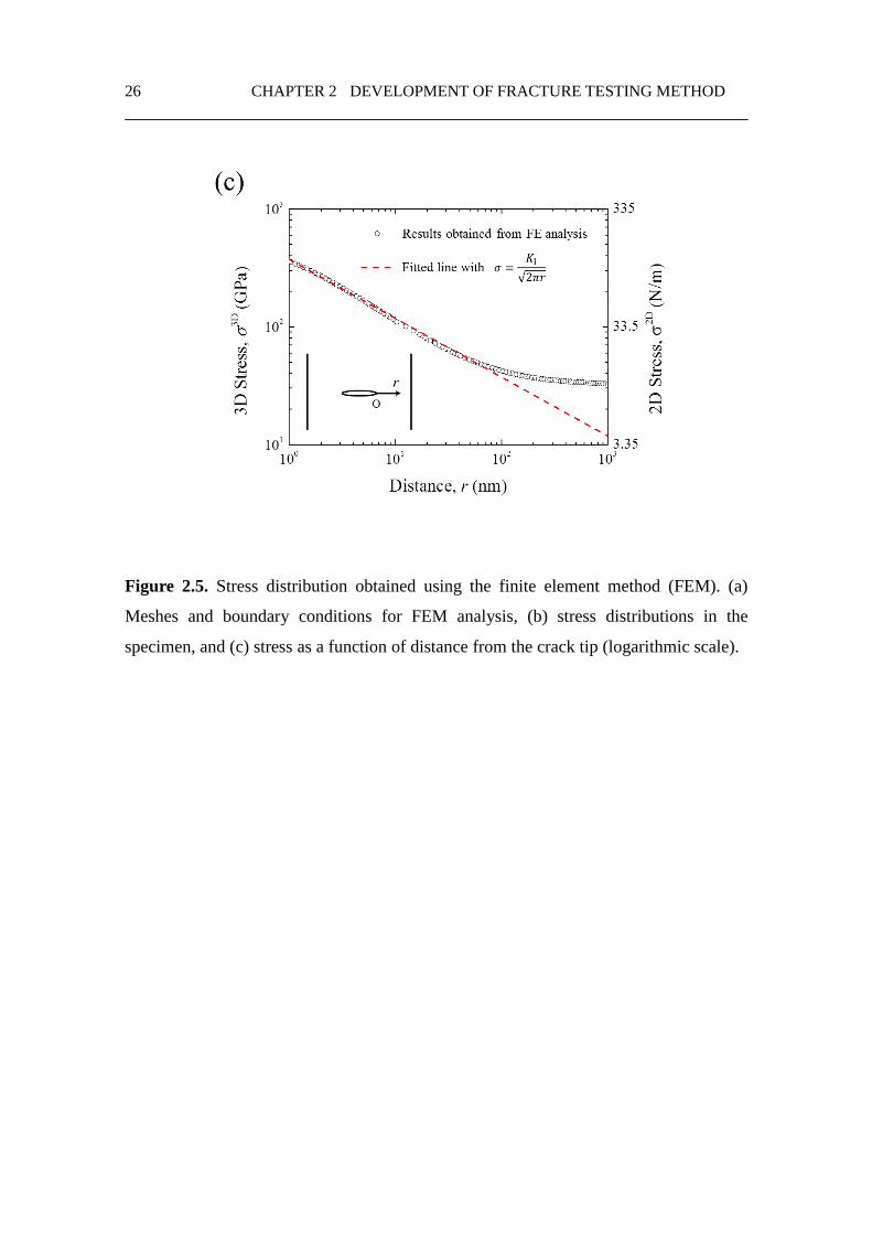
26 CHAPTER 2 DEVELOPMENT OF FRACTURE TESTING METHOD
Figure 2.5. Stress distribution obtained using the finite element method (FEM). (a)
Meshes and boundary conditions for FEM analysis, (b) stress distributions in the
specimen, and (c) stress as a function of distance from the crack tip (logarithmic scale).
2.4 CONCLUSIONS 27
2.4 Conclusion
In this chapter, the fracture behavior of bilayer graphene with a pre-crack was
investigated by in situ tensile testing in a SEM. I proposed a fracture testing method for
pristine graphene with nanoscale thickness, a machined pre-crack, and micro-scale width,
from preparation of the specimen to in situ examination and experiments. In the specimen
preparation, freestanding tensile specimens of atomically thin layers were fabricated by
the transfer technique with precise alignments. Pre-crack machining with gentle beam of
FIB realized sharp pre-crack fabrication at accurate position and shape, without
surrounding damages. The specimen is tested in SEM to align between the specimen and
loading axis, and to visualize crack propagation in the specimen. Applied load and
displacement was obtained from the fracture test. From the experimental results, Young’s
modulus and the stress field near the pre-crack was derived with the help of FE analyses.
In addition, high resolution SEM image presented the crack propagation and other
fracture characteristics in graphene. To confirm the fracture testing method, bilayer
graphene specimen is tested. Young’s modulus showed a reasonable value compared with
previous research. Additionally, I confirmed the brittle and unstable fracture behavior of
graphene with in situ observations. I also estimated the plane stress fracture toughness,
KC, of the graphene assuming a linear elastic constitutive relationship.
To characterize fracture behavior of graphene, it is necessary to test with the graphene
specimen with various dimension, and various crack size. Hence, more researches on
fracture of graphene are expected using the established methods in this chapter.
Furthermore, this methodology could be an insightful guideline for fracture tests for other
two-dimensional materials, such as boron nitride, molybdenum disulfide, silicene, and
black phosphorus. As material changed, the specimen fabrication process might be
modified

28 CHAPTER 2 DEVELOPMENT OF FRACTURE TESTING METHOD
REFERENCES 29
References
[1] K.S. Novoselov, A.K. Geim, S.V. Morozov, D. Jiang, Y. Zhang, S.V. Dubonos, I.V.
Grigorieva, A.A. Firsov, Electric field effect in atomically thin carbon films, Science
306 (2004) 666-669.
[2] X. Wang, X. Li, L. Zhang, Y. Yoon, P.K. Weber, H. Wang, J. Guo, H. Dai, N-doping
of graphene through electrothermal reactions with ammonia, Science 324 (2009) 768-
771.
[3] C. Lee, X. Wei, J.W. Kysar, J. Hone, Measurement of the elastic properties and
intrinsic strength of monolayer graphene, Science 321 (2008) 385-388.
[4] W. Quyang, X.-Z. Liu, Q. Li, Y. Zhang, J. Yang, Q. Zheng, Optical methods for
determining thickness of few-layer graphene flakes, Nanotechnology 24 (2013)
505701.
[5] A. Zurutuza, C. Marinelli, Challenges and opportunities in graphene
commercialization, Nature Nanotech. 9 (2014) 730-734.
[6] B.J. Kim, H. Jang, S.-K. Lee, B.H. Hong, J.-H. Ahn, J.H. Cho, High-performance
flexible graphene field effect transistors with ion gel gate dielectrics, Nano Lett. 10
(2010) 3464-3466.
[7] T.-H. Han, Y. Lee, M.-R. Choi, S.-H. Woo, S.-H. Bae, B.H. Hong, J.-H. Ahn, T.-W.
Lee, Extremely efficient flexible organic light-emitting diodes with modified
graphene anode, Nat. Photonics 6 (2012) 105-110.
[8] D. Choi, M.-Y. Choi, W.M. Choi, H.-J. Shin, H.-K. Park, J.-S. Seo, J. Park, S.-M.
Yoon, S.J. Chae, Y.H. Lee, S.-W. Kim, J.-Y. Choi, S.Y. Lee, J.M. Kim, Fully rollable
transparent nanogenerators based on graphene electrodes, Adv. Mater. 22 (2010)
2187-2192.

30 CHAPTER 2 DEVELOPMENT OF FRACTURE TESTING METHOD
[9] M.F. El-Kady, V. Strong, S. Dubin, R.B. Kaner, Laser scribing of high-performance
and flexible graphene-based electrochemical capacitors, Science 335 (2012) 1326-
1330.
[10] Y. Wang, R. Yang, Z. Shi, L. Zhang, D. Shi, E. Wang, G. Zhang, Super-elastic
graphene ripples for flexible strain sensors, ACS Nano 5 (2011) 3645-3650.
[11] T. Ramanathan, A.A. Abdala, S. Stankovich, D.A. Dikin, R.D. Herrera-Alonso, R.D.
Piner, D.H. Adamson, H.C. Schniepp, X. Chen, R.S. Ruoff, S.T. Nguyen, I.A. Aksay,
R.K. Prud’homme, L.C. Brinson, Functionalized graphene sheets for polymer
nanocomposites, Nature Nanotech 3 (2008) 327-331.
[12] Q. Zhang, X. Xu, D. Lin, W. Chen, G. Xiong, Y. Yu, T.S. Fisher, H. Li,
Hyperbolically patterned 3D graphene metamaterial with negative Poisson’s ratio
and superelasticity. Adv. Mater. 28 (2016) 2229-2237.
[13] K.-S. Kim, H.-J. Lee, C. Lee, S.-K. Lee, H. Jang, J.-H. Ahn, J.-H. Kim, H.-J. Lee,
Chemical vapor deposition-grown graphene: the thinnest solid lubricant, ACS Nano
5 (2011) 5107-5114.
[14] S. Won, Y. Hwango, S.-K. Lee, K.-S. Kim, K.-S. Kim, S.-M. Lee, H.-J. Lee, J.-H.
Ahn, J.-H. Kim, S.-B. Lee, Double-layer CVD graphene as stretchable transparent
electrodes, Nanoscale 6 (2014) 6057-6064.
[15] J. Kang, S. Hwang, J.H. Kim, M.H. Kim, J. Ryu, S.J. Seo, B.H. Hong, M.K. Kim,
J.-B. Choi, Efficient transfer of large-area graphene films onto rigid substrates by hot
pressing, ACS Nano 6 (2012) 5591–5598.
[16] F. Liu, P. Ming, J. Li, Ab initio calculation of ideal strength and phonon instability
of graphene under tension, Phys. Rev. B 76 (2007) 054120.
[17] A. Omeltchenko, J. Yu, R.K. Kalia, P. Vashishta, Crack front propagation and
fracture in a graphite sheet: A molecular-dynamics study on parallel computers, Phys.
Rev. Lett. 78 (1997) 2148-2151.
[18] H.I. Rasool, C. Ophus, W.S. Klug, A. Zettl, J.K. Gimzewski, Measurement of the
intrinsic strength of crystalline and polycrystalline graphene, Nat. Commun. 4 (2013)
2811.
[19] J. Han, N.M. Pugno, S. Ryu. Nanoindentation cannot accurately predict the tensile
strength of graphene or other 2D materials. Nanoscale 7 (2015) 15672-15679.

REFERENCES 31
[20] Y. Hwangbo, C.-K. Lee, S.-M. Kim, J.-H. Kim, K.-S. Kim, B. Jang, H.-J. Lee, S.-K.
Lee, S.-S. Kim, J.-H. Ahn, S.-M. Lee, Fracture characteristics of monolayer CVD-
graphene. Sci. Rep. 4 (2014) 4439.
[21] P. Zhang, L. Ma, F. Fan, Z. Zeng, C. Peng, P.E. Loya, Z. Liu, Y. Gong, J. Zhang, X.
Zhang, P.M. Ajayan, T. Zhu, J. Lou, Fracture toughness of graphene, Nat. Commun.
5 (2014) 3782.
[22] X. Wei, S. Xiao, F. Li, D.-M. Tang, Q. Chen, Y. Bando, D. Golberg, Comparative
fracture toughness of multilayer graphenes and boronitrenses, Nano. Lett. 15 (2015)
689-694.
[23] L. Colombo, X. Li, B. Han, C. Magnuson, W. Cai, Y. Zhu, R.S. Ruoff, Growth
kinetics and defects of CVD graphene on Cu, ECS Transactions 28 (2010) 109-114.
[24] P.Y. Huang, C.S. Ruiz-Vargas, A.M. van der Zande, W.S. Shitney, M.P. Levendorf,
J.W. Kevek, S. Garg, J.S. Alden, C.J. Hustedt, Y. Zhu, J. Park, P.L. McEuen, D.A.
Muller, Grains and grain boundaries in single-layer graphene atomic patchwork quilts,
Nature 469 (2011) 389-393.
[25] A.E. Mag-isa, C.-K. Lee, S.-M. Kim, J.-H. Kim, C.-S. Oh, Rapid determination of
the number of graphene layers by relative luminance, Carbon 94 (2015) 646-640.
[26] C.-K. Lee, Y. Hwangbo, S.-M. Kim, S.-K. Lee, S.-M. Lee, S.-S. Kim, K.-S. Kim,
H.-J. Lee, B.-Y. Choi, C.-K. Song, J.-H. Ahn, J.-H. Kim, Monoatomic chemical-
vapor-deposited graphene membranes bridge a half-millimeter-scale gap, ACS Nano
8 (2014) 2336-2344.
[27] Z. Liao, T. Zhang, M. Gall, A. Dianat, R. Rosenkranz, R. Jordan, G. Cuniberti, E.
Zschech, Lateral damage in graphene carved by high energy focused gallium ion
beams, Appl. Phys. Lett. 107 (2015) 013108.
[28] B.W. Smith, D.E. Luzzi, Electron irradiation effects in single wall carbon nanotubes,
J. Appl. Phys. 90 (2001) 3509-3515.
[29] A.C. Ferrari, J.C. Meyer, V. Scardaci, C. Casiraghi, M. Lazzeri, F. Mauri, S. Piscanec,
D. Jiang, K.S. Novoselov, S. Roth, A.K. Geim, Raman spectrum of graphene and
graphene layers, Phys. Rev. Lett. 97 (2006) 187401.
[30] H. Yin, H.J. Qi, F. Fan, T. Zhu, B. Wang, Y. Wei, Griffith criterion for brittle fracture
in graphene, Nano Lett. 15, (2015) 1918-1924.

32 CHAPTER 2 DEVELOPMENT OF FRACTURE TESTING METHOD
[31] D. Datta, S.P.V. Nadimpalli, Y. Li, V.B. Shenoy, Effect of crack length and
orientation on the mixed-mode fracture behavior of graphene, Extreme Mech. Lett. 5
(2015) 10-17.
[32] L. Zhou, Y. Wang, G. Cao, Elastic properties of monolayer graphene with different
chiralities, J. Phys.: Condens. Matter. 25 (2013) 125302.
[33] C. Lee, X. Wei, Q. Li. R. Carpick, J.W. Kysar, J. Hone, Elastic and frictional
properties of graphene, Phys. Status. Solidi. B 246 (2009) 2562-2567.
[34] Y. Zhang, C. Pan, Measurement of mechanical properties and number of layers of
graphene from nano-indentation, Diam. Relat. Mater. 24 (2012) 1-5.
[35] J.-U. Lee, D. Yoon, H. Cheong, Estimation of Young’s modulus of graphene by
Raman spectroscopy, Nano Lett. 12 (2012) 4444-4448.
[36] E. Cadelano, P.L. Palla, S. Giordano, L. Colombo, Nonlinear elasticity of monolayer
graphene, Phys. Rev. Lett. 102 (2009) 235502.
[37] Q. Lu, R. Huang, Nonlinear mechanics of single-atomic-layer graphene sheets, Int.
J. Appl. Mech. 1 (2009) 443-467.
[38] S. Singh, B.P. Patel, Nonlinear elastic properties of graphene sheet under finite
deformation, Compos. struct. 119 (2015) 412-421.
[39] J.W. Hutchinson, Singular behaviour at the end of a tensile crack in a hardening
material, J. Mech. Phys. Solids. 16 (1968) 13-31.
[40] J.R. Rice, A path independent integral and the approximate analysis of strain
concentration by notches and cracks, J. Appl. Mech. 35 (1968) 379-386.
33
Chapter 3
Fracture characteristics of multilayer graphene
3.1 Introduction
Griffith’s pioneering studies on the brittle fracture of materials triggered additional
research on fracture mechanics [1]. The stress intensity factor, K, introduced by Irwin,
characterizes the stress condition near the crack tip and explains the crack-driving force
based on linear elastic fracture mechanics (LEFM) [2]. The field of fracture mechanics
has been extended to nonlinear materials, allowing fracture phenomena in nonlinear
elastic materials to be elucidated [3,4,5]. Thus, the field of fracture mechanics has led to
the establishment of a theoretical framework for the design and engineering of bulk
materials for industries that demands high reliability [6]. However, at the nanoscale,
fracture mechanics confront new challenges. It is known that the fracture mechanics of
nanoscale materials are significantly different from those on the macroscopic scale [7]. In
particular, thin films have unique fracture characteristics; this has an effect on the
development of semiconducting devices as well as devices such as displays and energy
harvesters [8]. Thus, there are extensive research efforts underway to elucidate the
fracture mechanics of nanoscale materials; however, the nanoscale experiments involved
in such studies remain a challenge [9]. Graphene, which is an atomically thin carbon layer
and can be considered the ultimate thin material, is a fascinating model material for
studying fracture mechanics of nanoscale materials.
34 CHAPTER 3 FRACTURE CHARACTERISTICS OF MULTILAYER GRAPHENE
Graphene shows unique mechanical properties. For instance, it has an ultra-high
intrinsic strength and modulus, which originate from sp2-bonding, as measured
experimentally by nanoindentation.10 Further, it undergoes brittle fracture. The fracture
toughness of monolayer graphene is approximately 4.0 MPa√m; this has been confirmed
both experimentally and theoretically [11,12]. In addition, it has been reported that the
fracture toughness of multilayer graphene is higher than that of monolayer graphene
[13,14]. However, the fracture characteristics of multilayer graphene remain unclear. A
study on the mechanical behavior of multilayer graphene reported that it exhibits
interesting phenomena, such as interlayer slippages during loading and recovery during
unloading, and step by step fracture of stacked graphene [15,16]. However to our
knowledge, there have been no scrutinized studies on the effect of these phenomena on
the fracture characteristics of multilayer graphene. In addition, most experimental studies
on the fracture mechanics of graphene has been performed based on LEFM [11,13,14,17],
and few analytical studies have considered the nonlinear behavior of graphene, which
shows nonlinearities related to nonlinear elastic material properties [18,19].
Conventionally, experimental researches on nonlinear elastic fracture mechanics have
been mainly discussed for elastic plastic materials. In nonlinear elastic fracture mechanics,
however, there are a few studies for nonlinear elastic materials and no researches in
atomic scale, to our best knowledge.
Multilayer graphene shows promise as a structural material for use in composite
materials that need to be light-weight and show high strength and toughness [20]. Such
composite materials are usually composed of exfoliated graphene flakes that consist of
several layers and polymer matrix to bind the flakes [21]. To be able to optimize the
mechanical properties of composite materials based on multilayer graphene flakes, a
complete understanding of the mechanical behavior of multilayer graphene is essential.
This is because the failure mechanisms of such composites are closely related to the
failure of the individual multilayer graphene flakes present in them [22]. There are only
a few studies on the fracture characteristics of multilayer graphene, and several
obscurities still remain and hinder multilayer graphene from wide-spread usage.
In this chapter, single crystalline multilayer graphene specimens with a single edge
crack were measured by in situ mode I fracture tests under a scanning electron microscope

3.2 EXPERIMENTAL 35
(SEM). The testing method developed in the chapter 2 is utilized from the fabrication of
the specimen and the in situ fracture testing. The elastic modulus and fracture toughness
of the graphene specimens were determined from the measured load-displacement curves
through finite element analysis (FEA). The constitutive nonlinearity of graphene was
considered from a viewpoint of nonlinear elastic fracture mechanics. Moreover, unique
crack propagation and toughening of multilayer graphene was analyzed and its underlying
mechanism was elucidated.
3.2 Experimental
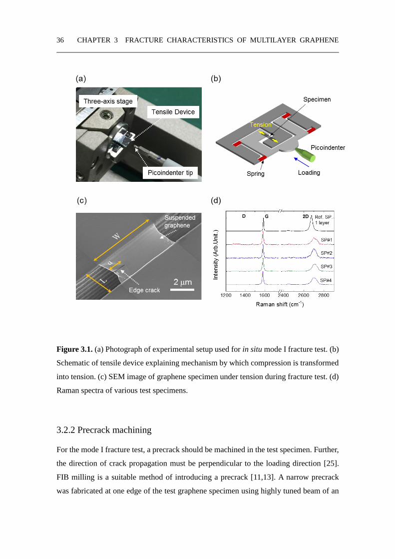
3.2.1 Specimen fabrication
Freestanding graphene specimens for the mode I fracture test were fabricated by the
high-alignment-precision transfer method developed by Jang, et al [13]. Pristine graphene
was obtained by the repeated peeling of highly oriented pyrolytic graphite using a piece
of Scotch tape [23]. To be able to visually observe and select multilayer graphene, the
mechanically exfoliated graphene was transferred on a silicon wafer with 300-nm-thick
silicon dioxide layer [24]. Using an optical microscope, strip-like graphene specimens
with a width of 4–
was used as the loading apparatus for the tests, as shown in Figure 3.1(a). The graphene
specimens were transferred onto a PTP device (Push-to-Pull, Hysitron), which can
convert compression into tension, as shown in the schematic of Figure 3.1(b). The
graphene specimens were transferred using a polymethyl methacrylate layer, which was
eventually removed using acetone in the final step of the process. In addition, an optical
microscope was used to align the test specimen and the PTP device with precision.
36 CHAPTER 3 FRACTURE CHARACTERISTICS OF MULTILAYER GRAPHENE
Figure 3.1. (a) Photograph of experimental setup used for in situ mode I fracture test. (b)
Schematic of tensile device explaining mechanism by which compression is transformed
into tension. (c) SEM image of graphene specimen under tension during fracture test. (d)
Raman spectra of various test specimens.
3.2.2 Precrack machining
For the mode I fracture test, a precrack should be machined in the test specimen. Further,
the direction of crack propagation must be perpendicular to the loading direction [25].
FIB milling is a suitable method of introducing a precrack [11,13]. A narrow precrack
was fabricated at one edge of the test graphene specimen using highly tuned beam of an
3.2 EXPERIMENTAL 37
FIB milling system (FB2200, Hitachi), as shown in Figure 3.1(c). Because a graphene
specimen with a single edge crack would have just one crack tip, which would also be the
crack initiation point, observing the crack propagation path is convenient at fracture. After
the specimens for the fracture test has been fabricated, they were characterized using SEM
and Raman spectroscopy. The dimensions of the specimens as well as those precracks
were determined from the SEM images.
3.2.3 In situ mode I fracture test
The in situ mode I fracture tests were performed using a picoindenter under SEM
(SU8250, Hitachi). The tensile device was mounted on three-axis piezo actuator, so that
the loading tip of the picoindenter could push at the desired point of the tensile device
with the help of the SEM system. The load applied to the graphene specimen was
calibrated using four springs of the tensile device, as shown in Figure 3.1(b). The
displacement was obtained from the controller of the picoindenter, and calibrations were
performed based on digital image correlation using the SEM images. This was because
the stiffness of the tensile device and the indenter tip as well as the contact point can lead
to errors in the displacement data. The displacement was controlled using PID control
parameters, and the strain rate during the test was approximately 3.1 × 10⁻³ s-1.
3.2.4 Finite element analysis
To analyze the experimental results, numerical FEA simulations were performed using
the commercial code, ABAQUS. The geometries of all the test specimens were precisely
copied with FEA model. The thickness of a monolayer graphene was assumed to be 0.335
nm, which is the average interlayer distance of graphite layers. Moreover, two-
dimensional plane stress elements were used for the analyses. Since the experiments were
performed under the condition of displacement control, the boundary conditions were that
the nodes of the bottom edge were fixed while the nodes of the top edge were subjected
to uniform displacements. Because graphene exhibits a large failure strain up to 25% [10],
finite deformation was considered for the FEA. For the linear elastic analysis, the
38 CHAPTER 3 FRACTURE CHARACTERISTICS OF MULTILAYER GRAPHENE
experimentally determined elastic modulus was used. The nonlinear elastic analysis was
performed using the stress-strain relationship from the reference calculated by molecular
dynamic simulation [18].
3.3 Results and discussions
3.3.1 Fracture toughness of multilayer graphene
A specimen of multilayer graphene used in mode I fracture test is shown in the SEM
image of Figure 3.1(c). A precrack was machined in the direction perpendicular to the
loading axis with focused ion beam (FIB). A total of four specimens (SP#1 to SP#4) were
tested. The number of layers in the multilayer graphene specimens could be determined
based on the shape of the 2D band in their Raman spectrum, as shown in Figure 3.1(d)
[26]. In addition, the fact that the small D peak of every spectrum had a low intensity
confirmed that all the pristine graphene specimens contained very few atomistic defects.
The width (W), the crack length (a), and the number of layers of the specimens are listed
in Table 1. During the test, the load applied to the test specimen and the resultant
displacement between the grips were measured, and in situ SEM imaging was performed.
In keeping with previous reports, all the specimens exhibited brittle fracture. The fractures
were initiated at the crack tips machined using FIB [11,13,14]. Figure 3.2(a) shows a
representative load-displacement curve of a graphene fracture specimen (SP#1), which
was three layers. The points marked (A)-(F) in the graph represent the characteristic states
during the test. In the initial state (A), the specimen exhibited a negative residual strain
owing to the mismatch strain between itself and the push-to-pull (PTP) device; this strain
was taken into account during the strain calibration process. During the test, two load
drops were observed; thus the curve could be divided into two parts, C1 and C2. In the
first part, C1, the applied load increases monotonically, with the stiffness of the tri-layer
graphene specimen being 1170 N/m. After state (C), the crack propagates unstably from
the precrack tip, as can be seen from SEM image (D) in Figure 3.2(b). The failure load,
Pf, was 37.7 N. The crack was arrested in the middle of the specimen, with the load
increasing to that corresponding to state (E). The stiffness corresponding to part C2 of the
curve, obtained by linear fitting, was 450 N/m; this was because the compliance of the
3.3 RESULTS AND DISCUSSIONS 39
specimen increased with the extension of the crack. After the complete failure of the
specimen, it was possible to determine the crack path from in situ SEM image (F). The
crack grew perpendicular to the loading direction globally but locally changed its
direction during propagation.
The elastic modulus could not be determined directly from the experiments owing to
the complex geometry of the cracked specimens; however, it was possible to obtain the
elastic modulus using FEA and the measured stiffness. For the four test specimens, the
average elastic modulus was 732±37.3 MPa. Although, this value is apparently lower
than monolayer graphene (elastic modulus of 0.8–1.1 TPa), it shows good agreement with
the results of a molecular dynamics simulation of multilayer graphene [10,27]. The red
dotted line in Figure 3.2(a) represents the calculated stiffness of the specimen, SP#1. In
SEM image (E) of Figure 3.2(b), the position of the arrested crack tip can be identified.
Further, the propagation length of the crack is 3.9 m. To analyze part C2 of the curve,
the actual geometry of the specimen with the arrested crack was modeled based on the
SEM image using the finite element method (FEM). Using the same conditions as those
employed for the analysis of part C1, the load-displacement curve obtained by FEM is
shown as blue dotted line in Figure 3.2(a). It can be seen that it fits the experimental
results well.
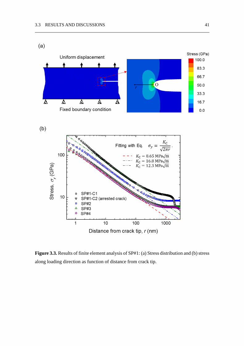
Figure 3.3(a) shows the stress distribution at the moment of fracture of SP#1. The far-
field stress, f, is 4.9 GPa at the time of failure, and the corresponding strain is 0.7%. The
nominal stress, y, as a function of the distance from the precrack tip, r, is plotted in
Figure 3.3(b). Based on LEFM, the graph was fitted using the function,
𝜎𝑦 =𝐾C
√2𝜋𝑟 , (1)
where KC denotes the plane stress fracture toughness. The fracture toughness of the tested
specimens, obtained by fitting their stress distributions, are listed in Table 1. With the
exception of the specimen in which the crack was arrested (SP#1-C2) and specimen SP#2,
the rest of the specimens had an average fracture toughness of 8.65±0.46 MPa√m, which
is much higher than that of monolayer graphene, but consistent with that reported in the
literature for multilayer graphene [14]. The even higher fracture toughness obtained for
SP#1-C2 and SP#2 are explained in the subsequent sections.

40 CHAPTER 3 FRACTURE CHARACTERISTICS OF MULTILAYER GRAPHENE
Figure 3.2. (a) Force-displacement curve of SP#1 as determined from facture test. (b) In
situ SEM images corresponding to points (A)-(F) in Figure 3.2(a). Scale bars are 3 m.
In set figure of (E) is magnified and filtered image of rectangular region of dotted line in
the image.
3.3 RESULTS AND DISCUSSIONS 41
Figure 3.3. Results of finite element analysis of SP#1: (a) Stress distribution and (b) stress
along loading direction as function of distance from crack tip.
42 CHAPTER 3 FRACTURE CHARACTERISTICS OF MULTILAYER GRAPHENE
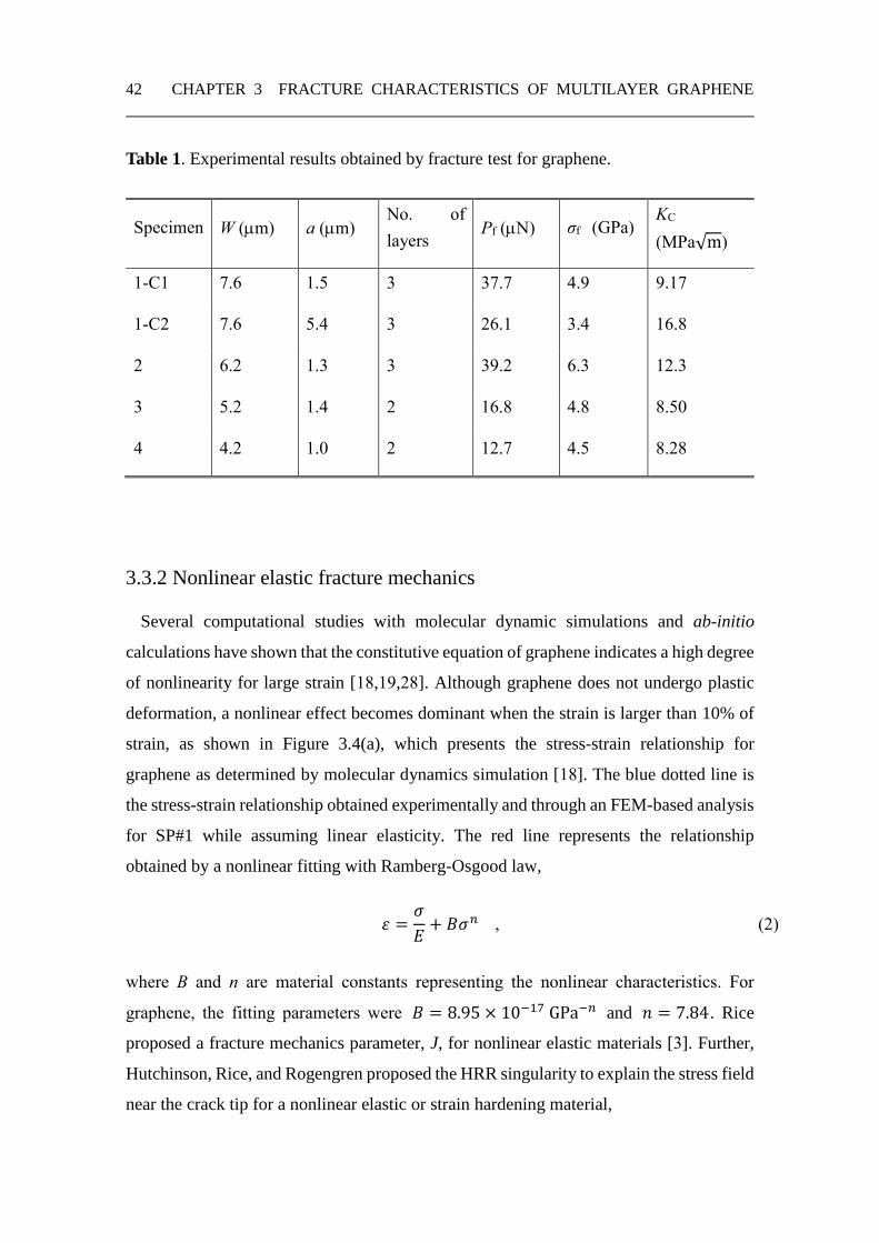
Table 1. Experimental results obtained by fracture test for graphene.
Specimen W (m) a (m) No. of
layers Pf (N) σf (GPa)
KC
(MPa√m)
1-C1 7.6 1.5 3 37.7 4.9 9.17
1-C2 7.6 5.4 3 26.1 3.4 16.8
2 6.2 1.3 3 39.2 6.3 12.3
3 5.2 1.4 2 16.8 4.8 8.50
4 4.2 1.0 2 12.7 4.5 8.28
3.3.2 Nonlinear elastic fracture mechanics
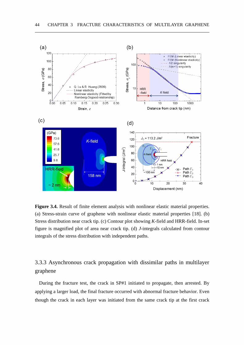
Several computational studies with molecular dynamic simulations and ab-initio
calculations have shown that the constitutive equation of graphene indicates a high degree
of nonlinearity for large strain [18,19,28]. Although graphene does not undergo plastic
deformation, a nonlinear effect becomes dominant when the strain is larger than 10% of
strain, as shown in Figure 3.4(a), which presents the stress-strain relationship for
graphene as determined by molecular dynamics simulation [18]. The blue dotted line is
the stress-strain relationship obtained experimentally and through an FEM-based analysis
for SP#1 while assuming linear elasticity. The red line represents the relationship
obtained by a nonlinear fitting with Ramberg-Osgood law,
𝜀 =𝜎
𝐸+ 𝐵𝜎𝑛 , (2)
where B and n are material constants representing the nonlinear characteristics. For
graphene, the fitting parameters were 𝐵 = 8.95 × 10⁻¹⁷ GPa−𝑛 and 𝑛 = 7.84. Rice
proposed a fracture mechanics parameter, J, for nonlinear elastic materials [3]. Further,
Hutchinson, Rice, and Rogengren proposed the HRR singularity to explain the stress field
near the crack tip for a nonlinear elastic or strain hardening material,
3.3 RESULTS AND DISCUSSIONS 43
𝜎 = 𝑘 (𝐽
𝑟)
1𝑛+1
, (3)
where k is proportional constant [4,5]. When 𝑛 = 1, Eq. (3) is equivalent to Eq. (1) which
is based on LEFM.
To elucidate the nonlinear fracture behavior of graphene, a numerical computation for
specimen SP#1 was performed using FEA with the parameters representing nonlinear
elastic material properties of graphene. In addition, the nonlinearity related to finite
deformation was taken into account in the calculation to simulate large deformation in
the vicinity of the precrack tip. This means that both geometry and constitutive
nonlinearities were considered during the FEA simulation. Figure 3.4(b) describes the
stress field near the crack tip. Like the stress distribution obtained by FEA based on linear
elasticity, it shows a (−1
2) singularity and could be fitted well using Eq. (1) in the inner
region starting from 158 nm. However, the stress distribution calculated using the
nonlinear elastic properties contains an HRR-field defined by Eq. (3) and it shows a
(−1
𝑛+1) singularity near the crack tip, which had a size of 2 nm. Therefore, we confirmed
that the stress field of a cracked graphene specimen has both a K-field and an HRR-field
near the crack tip. When the size of the specimen is much larger than that of the K-field,
the fracture characteristics of graphene can be evaluated based on the parameter KC like
the cases in this study. This was confirmed by the J-integral calculated from the contour
integral, which is integrated using independent paths (1-3), as shown in Figure 3.4(d).
The critical value of J at fracture, JC, is 113.2 J/m2, which is in keeping with the
relationship, 𝐽C = 𝐾C2/𝐸 , for linear elastic materials under a plane stress condition.
However, specimens with a width smaller than 100 nm or those with a very long crack
may have the dominant HRR-field and very small K-field near the crack tip [14]. In these
cases, JC should be evaluated as the fracture parameter instead of KC.
44 CHAPTER 3 FRACTURE CHARACTERISTICS OF MULTILAYER GRAPHENE
Figure 3.4. Result of finite element analysis with nonlinear elastic material properties.
(a) Stress-strain curve of graphene with nonlinear elastic material properties [18]. (b)
Stress distribution near crack tip. (c) Contour plot showing K-field and HRR-field. In-set
figure is magnified plot of area near crack tip. (d) J-integrals calculated from contour
integrals of the stress distribution with independent paths.
3.3.3 Asynchronous crack propagation with dissimilar paths in multilayer
graphene
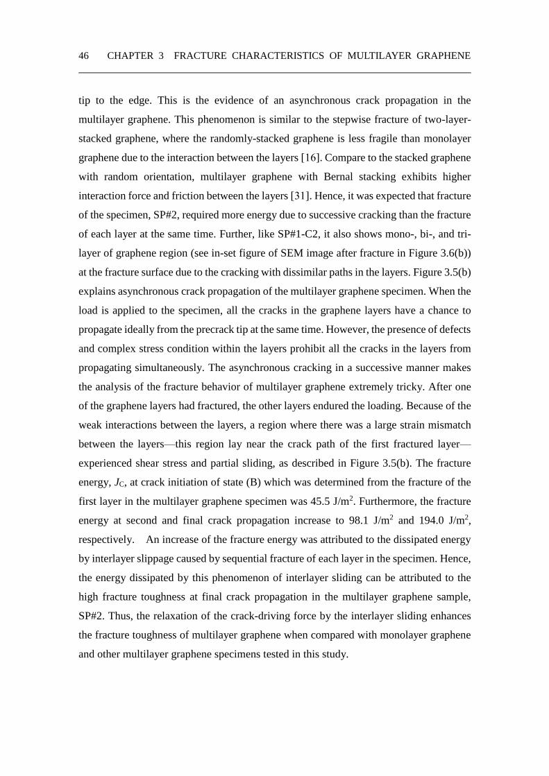
During the fracture test, the crack in SP#1 initiated to propagate, then arrested. By
applying a larger load, the final fracture occurred with abnormal fracture behavior. Even
though the crack in each layer was initiated from the same crack tip at the first crack
3.3 RESULTS AND DISCUSSIONS 45
propagation in state (C) of Figure 3.2(a), the cracks propagated along with dissimilar
paths among the three layers. This was because of the noncovalent interaction between
the adjacent layers of the multilayer graphene sample. Multilayer graphene has the weak
adhesion among the layers, originated from π electron interaction and van der Waals
interaction, unlike strong sp2 interaction in in-plane structure [15,29,30]. Therefore, crack
propagation in multilayer graphene is affected by these anisotropic interaction structures.
The crack propagation with dissimilar paths could be confirmed by the fracture surface
(see SEM image (F) of Figure 3.2(b)) taken after the final fracture of the specimen. In
addition, the position of the arrested crack tip of each layer did not coincide with each
other. In Figure 3.5(a), the upper figure describes the interlayer-mismatched crack tips
for arrested cracks with dissimilar paths. Near the crack tips, the stress and strain was
concentrated. This means an area with a misfit stress existed between the adjacent layers
of the graphene sample, causing a shear stress between them, as shown in the cross-
sectional image of Figure 3.5(a). This shear stress induced interlayer slippage and energy
dissipation during the loading of the specimen [15]. Hence it can be concluded that the
fracture toughness of specimen with the arrested crack (SP#1-C2) was large owing to the
crack propagation with dissimilar paths in the adjacent layers.
The weak interactions between the layers of multilayer graphene lead another abnormal
fracture behavior. The cracks in each layer not only propagate along with dissimilar paths,
but also propagate asynchronously. Figure 3.6(a) shows the load-displacement curve for
SP#2, and the movie in the Supporting Information displays the crack propagation at
fracture. The graph shows that three load drops occur before the complete failure of the
specimen, and can be divided into three parts, C1 to C3. After first and second load drops,
the corresponding in situ SEM images ((C) and (E), respectively, Figure 3.6(b)) did not
indicate crack propagation. However, the stiffnesses as determined from parts C1 and C2
were two and three times higher than that corresponding to part C3, respectively. This
means that three layer of the multilayer graphene sample fractured one by one at each
load drop. An FEA simulation using a graphene specimen with the same geometry
showed that the change in the stiffness was attributable to a decrease in the thickness of
the specimen. An SEM image obtained after the final fracture of the specimen (see Figure
3.6(b)) shows that the cracks in all the layers had propagated from the machined precrack
46 CHAPTER 3 FRACTURE CHARACTERISTICS OF MULTILAYER GRAPHENE
tip to the edge. This is the evidence of an asynchronous crack propagation in the
multilayer graphene. This phenomenon is similar to the stepwise fracture of two-layer-
stacked graphene, where the randomly-stacked graphene is less fragile than monolayer
graphene due to the interaction between the layers [16]. Compare to the stacked graphene
with random orientation, multilayer graphene with Bernal stacking exhibits higher
interaction force and friction between the layers [31]. Hence, it was expected that fracture
of the specimen, SP#2, required more energy due to successive cracking than the fracture
of each layer at the same time. Further, like SP#1-C2, it also shows mono-, bi-, and tri-
layer of graphene region (see in-set figure of SEM image after fracture in Figure 3.6(b))
at the fracture surface due to the cracking with dissimilar paths in the layers. Figure 3.5(b)
explains asynchronous crack propagation of the multilayer graphene specimen. When the
load is applied to the specimen, all the cracks in the graphene layers have a chance to
propagate ideally from the precrack tip at the same time. However, the presence of defects
and complex stress condition within the layers prohibit all the cracks in the layers from
propagating simultaneously. The asynchronous cracking in a successive manner makes
the analysis of the fracture behavior of multilayer graphene extremely tricky. After one
of the graphene layers had fractured, the other layers endured the loading. Because of the
weak interactions between the layers, a region where there was a large strain mismatch
between the layers—this region lay near the crack path of the first fractured layer—
experienced shear stress and partial sliding, as described in Figure 3.5(b). The fracture
energy, JC, at crack initiation of state (B) which was determined from the fracture of the
first layer in the multilayer graphene specimen was 45.5 J/m2. Furthermore, the fracture
energy at second and final crack propagation increase to 98.1 J/m2 and 194.0 J/m2,
respectively. An increase of the fracture energy was attributed to the dissipated energy
by interlayer slippage caused by sequential fracture of each layer in the specimen. Hence,
the energy dissipated by this phenomenon of interlayer sliding can be attributed to the
high fracture toughness at final crack propagation in the multilayer graphene sample,
SP#2. Thus, the relaxation of the crack-driving force by the interlayer sliding enhances
the fracture toughness of multilayer graphene when compared with monolayer graphene
and other multilayer graphene specimens tested in this study.
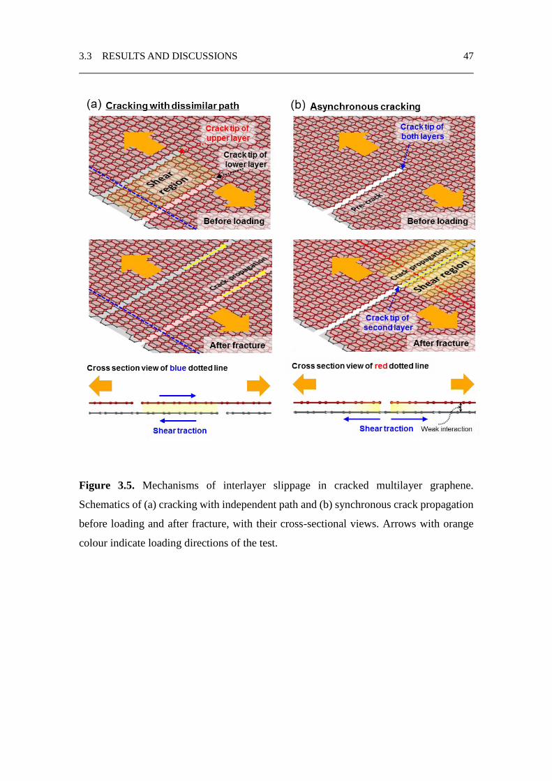
3.3 RESULTS AND DISCUSSIONS 47
Figure 3.5. Mechanisms of interlayer slippage in cracked multilayer graphene.
Schematics of (a) cracking with independent path and (b) synchronous crack propagation
before loading and after fracture, with their cross-sectional views. Arrows with orange
colour indicate loading directions of the test.
48 CHAPTER 3 FRACTURE CHARACTERISTICS OF MULTILAYER GRAPHENE
Figure 3.6. Results of fracture test for SP#2. (a) Load-displacement curve and (b) in situ
SEM images corresponding to points (A)-(D) in Figure 3.6(a) and that obtained after
specimen fracture. Scale bars are 3 m.

3.4 CONCLUSIONS 49
3.4 Conclusions
In this chapter, the fracture behavior of multilayer graphene using in situ mode I fracture
tests under SEM is investigated. Multilayer graphene specimen is fabricated using the
transfer process with precise alignments, and the single edge pre-crack on the specimen
is machined with FIB. From the fracture test, the fracture toughness was determined from
the measured load-displacement curve and FEA. And, the experimental results were
consistent with that reported in the literatures. The nonlinear elastic behavior of graphene
was discussed from the viewpoint of nonlinear fracture mechanics. Using nonlinear FEA,
it was confirmed that graphene exhibits the HRR-field as well as the K-field near the
crack tip. However, the dominant K-field implies that the parameter KC is applicable to
evaluating fracture characteristics of large graphene specimens with small cracks. In
addition, the cracks in the various layers propagate asynchronously along dissimilar paths
was observed in the in situ SEM experiments for the multilayer graphene specimen. These
abnormal crack propagations activated interlayer shear stress and interlayer slippage
originated from the weak interactions between the adjacent layers of the multilayer
graphene. This is the reason why the fracture toughnesses of these specimens were higher
than that of monolayer graphene.
. Graphene possess high stiffness and high strength. However, it is a brittle material so
that low fracture toughness has become obstacles for the application of graphene. The
enhancement of fracture toughness by interfacial sliding can provide the solutions of these
problems. Furthermore, these mechanisms can be applied in graphene on polymer
materials allowing large deformation. By sliding in the interface between graphene and
the polymer, graphene can toughen compared to freestanding graphene. Therefore these
toughening mechanisms of multilayer graphene could provide useful insight to
development of fabrication process for various flexible devices using graphene, and
design of such devices for a reliability
50 CHAPTER 3 FRACTURE CHARACTERISTICS OF MULTILAYER GRAPHENE
References
[1] A.A. Griffith, The phenomena of rupture and flow in solids, Philos. Trans. R. Soc.
London, Ser. A 221 (1921) 163–198.
[2] G.R. Irwin, Analysis of stresses and strains near the end of a crack traversing a plate,
J. Appl. Mech. 24 (1957) 361–364.
[3] J.R. Rice, A path independent integral and the approximate analysis of strain
concentration by notches and cracks, J. Appl. Mech. 35 (1968) 379–386.
[4] J.W. Hutchinson, Singular behavior at the end of tensile crack tip in a hardening
material, J. Mech. Phys. Solids 16 (1968) 13–31.
[5] J.R. Rice, G.F. Rosengren, Plane strain deformation near a crack tip in a power-law
hardening material, J. Mech. Phys. Solids, 16 (1968) 1–12.
[6] T.L. Anderson, Fracture Mechanics: Fundamentals and Applications. (CRC Press,
Boca Ranton, 2005)
[7] T. Kitamura, H. Hirakata, T. Sumigawa,T. Shimada, Fracture Nanomechanics. (CRC
Press, Boca Ranton, 2016)
[8] W.D. Nix, Mechanical properties of thin films, Metall. Trans. A. 20 (1989) 2217–
2245.
[9] M.A. Haque, M.T.A. Saif, A review of MEMS-based microscale and nanoscale tensile
and bending testing, Exp. Mech., 43 (2003) 248–255.
[10] C. Lee, X. Wei, J. W. Kysar, J. Hone, Measurement of the elastic properties and
intrinsic strength of monolayer graphene, Science 321 (2008) 385–388.
[11] P. Zhang, L. Ma, F. Fan, Z. Zeng, C. Peng, P.E. Loya, Z. Liu, Y. Gong, J. Zhang, X.
Zhang, P. M. Ajayan, T. Zhu, J. Lou, Fracture toughness of graphene, Nature
Commun. 5 (2014) 3782.

REFERENCES 51
[12] A. Omeltchenko, J. Yu, R.K. Kalia, P. Vashishta, Crack front propagation and
fracture in a graphite sheet: A molecular-dynamics study on parallel computers, Phys.
Rev. Lett. 78 (1997) 2148–2151.
[13] B. Jang, A.E. Mag-isa, J.-H. Kim, B. Kim, H.-J. Lee, C.-S. Oh, T. Sumigawa, T.
Kitamura. Uniaxial fracture test of freestanding pristine graphene using in situ tensile
tester under scanning electron microscope, Extreme Mech. Lett. (2016) DOI:
10.1016/ j.eml.2016.11.001.
[14] X. Wei, S. Xiao, F. Li, D.-M. Tang, Q. Chen, Y. Bando, D. Golberg, Comparative
fracture toughness of multilayer graphenes and boronitrenses, Nano Lett. 15 (2015)
689–694.
[15] X. Wei, Z. Meng, L. Ruiz, X. Xia, C. Lee, J.W. Kysar, J.C. Hone, S. Keten, H.D.
Espinosa, Recoverable slippage mechanism in multilayer graphene leads to
repeatable energy dissipation, ACS Nano 10 (2016) 1820–1828.
[16] Q.-Y. Lin, Y.-H. Zeng, D. Liu, G.Y. Jing, Z.-M. Liao, D. Yu, Step-by-step fracture
of two-layer stacked graphene membranes, ACS Nano 8 (2014) 10246-10251.
[17] Y. Hwangbo, C.-K. Lee, S.-M. Kim, J.-H. Kim, K.-S. Kim, B. Jang, H.-J. Lee, S.-K.
Lee, S.-S. Kim, J.-H. Ahn, S.-M. Lee, Fracture characteristics of monolayer CVD-
graphene, Sci. Rep. 4 (2014) 4439.
[18] Q. Lu, R. Huang, Nonlinear mechanics of single-atomic-layer graphene sheets, Int.
J. Appl. Mech. 1 (2009) 443–467.
[19] E. Cadelano, P.L. Palla, S. Giordano, L. Colombo, Nonlinear elasticity of monolayer
graphene, Phys. Rev. Lett. 102 (2009) 235502.
[20] R. Atif, I. Shyha, F. Inam, Mechanical, thermal, and electrical properties of
graphene-epoxy nanocomposites-a review, Polymers 8 (2016) 281.
[21] S. Stankovich, D.A. Dikin, G.H.B. Dommett, K.M. Kohlhaas, E.J. Zimney, E.A.
Stach, R.D. Piner, S.T. Nguyen, R.S. Ruoff, Graphene-based composite materials,
Nature 442 (2006) 282–286.
[22] S. Chandrasekaran, N. Sato, F. Tölle, R. Mülhaupt, B. Fiedler, Fracture toughness
and failure mechanism of graphene based epoxy composites, Compos. Sci. Technol.
97 (2014) 90–99.
52 CHAPTER 3 FRACTURE CHARACTERISTICS OF MULTILAYER GRAPHENE
[23] K.S. Novoselov, A.K. Geim, S.V. Morozov, D. Jiang, Y. Zhang, S.V. Dubonos, I.V.
Grigorieva and A.A. Firsov, Electric field effect in atomically thin carbon films,
Science 306 (2004) 666–669.
[24] P. Blake, E.W. Hill, Making graphene visible, Appl. Phys. Lett. 91 (2007) 063124.
[25] ASTM E1820-16, Standard Test Method for Measurement of Fracture Toughness.
(ASTM International, West Conshohocken, PA, 2016) www.astm.org.
[26] A.C. Ferrari, J.C. Meyer, V. Scardaci, C. Casiraghi, M. Lazzeri, F. Mauri, S. Piscanec,
D. Jiang, K.S. Novoselov, S. Roth, A.K. Geim, Raman spectrum of graphene and
graphene layers, Phys. Rev. Lett. 97 (2006) 187401.
[27] M.D. Jiao, L. Wang, C.Y. Wang, Q. Zhang, S.Y. Ye, F.Y. Wang, Molecular
dynamics simulations on deformation and fracture of bi-layer graphene with different
stacking pattern under tension, Phys. Lett. A 380 (2016) 609–613.
[28] X. Wei, B. Fragneaud, C.A. Marianetti, J.W. Kysar, Nonlinear elastic behavior of
graphene: Ab initio calculations to continuum description, Phys. Rev. B 80 (2009)
205407.
[29] R. Saito, R. Matsuo, T. Kimura, G. Dresselhaus, M.S. Dresselhaus, Anomalous
potential barrier of double-wall carbon nanotube, Chem. Phys. Lett. 348 (2001) 187–
193.
[30] L. Ruiz, W. Xia, Z. Meng, S. Keten, A coarse-grained model for the mechanical
behavior of multi-layer graphene, Carbon 82 (2015) 103–115.
[31] A. E. Filippov, M. Dienwiebel, J. W. M. Frenken, J. Klafter and M. Urbakh, Torque
and twist against superlubricity, Phys. Rev. Lett., 2008, 100, 046102.
53
Chapter 4
Reduction of fracture damage on graphene in transfer
process for transparent electrode
4.1 Introduction
Graphene has been regarded as one of the most promising materials in the fields of
display, semiconductor, and energy applications owing to its excellent physical properties
[1–3]. Its high electrical conductivity and optical transmittance are useful for transparent
electrodes for display and solar cell applications [3–6], and its high mechanical flexibility
is also attractive in the field of flexible transparent electrode [5–10]. Graphene can be
produced by several methods like chemical vapor deposition (CVD) on metallic catalyst,
epitaxial growth on SiC, micromechanical exfoliation from graphite, chemical and liquid
exfoliation, etc [1,11–13]. For the application of flexible transparent electrode, CVD-
graphene has advantages over other methods in terms of large area scalability, and high
and uniform electrical properties [3,5–10,12].
The fabrication of a graphene transparent flexible electrode necessitates the transfer
CHAPTER 4 REDUCTION OF FRACTURE DAMAGES ON GRAPHENE
54 IN TRANSFER PROCESS FOR FLEXIBLE CONDUCTIVE ELECTRODE
of CVD-graphene from a metallic catalyst to a polymeric film with high transparency and
flexibility. Due to the high temperature up to 1000 ◦C of standard CVD of graphene, it is
nearly impossible to directly synthesize graphene with high quality on a polymeric film,
and transferring CVD-graphene is inevitable. Lots of researchers have proposed several
transfer methods of CVD-graphene from a catalyst to a polymeric film, and the polymer-
layer-assisted transfer method has been considered as the most appropriate and
commercially viable one, which is an indirect transfer process based on polymer coatings
or carrier films [5,6]. The polymeric carrier films can be poly(methyl methacrylate)
(PMMA), poly(dimethyl siloxane) (PDMS), thermal release tape (TRT), and silicone-
coated poly(ethylene terephthalate) (PET). This polymeric carrier films robustly hold the
atomically thin graphene and protect it from mechanical damages during the transfer
process [3,5,7,12,14,15]. Furthermore, the polymer films play an import role to prevent
from brittle fracture of graphene. This is because the interaction between graphene and
the film dissipate the fracture energy during fracturing, which is the similar mechanisms
explained in chapter 3. On the other hand, the direct transfer of graphene on a polymeric
film involves lamination process between the polymeric film and CVD-graphene on a
metallic foil with an optically clear adhesive (OCA). This direct transfer can reduce the
process steps, but suffers from optical degradation and high cost of the adhesive, and
limitations in uniformity and scalability in the manufacturing of the graphene transparent
electrode [8,16–18].
Mass production of the graphene transparent electrode requires a roll-based synthesis,
a roll-based etching process, a roll-based transfer process, and a roll-based patterning
process [5,8,16,17,19]. The roll-based processes accompany mechanical contacts
between the graphene and a carrier film, or between graphene and a flexible substrate.
The graphene transferred on the flexible substrate is prone to be damaged from localized
contact pressure caused by mechanical compression of nip rolls during the roll transfer
process [20]. Mechanical deformations of graphene induced by complex stress
configurations are responsible for localized mechanical failures of graphene and result in
the degradation of its electrical performance. Thus, understanding of the failure
mechanisms of graphene during the roll transfer process is essential in developing a roll-
to-roll (R2R) transfer machine of a graphene flexible electrode with high throughput and
4.2 EXPERIMENTS AND RESULTS 55
high quality.
In this chapter, the reducing mechanical failures of graphene on a flexible substrate in
the roll-based transfer process was studied. For the fabrication of graphene transparent
electrode, monolayer graphene synthesized by the CVD process is transferred on PET
using an R2R transfer machine with a contact pressure control module. With respect to
the graphene films transferred with different contact pressures, mechanical damages
induced by high contact pressure were observed on the roll-transferred graphene using a
scanning electron microscope (SEM). The observation of damages enables the discussion
of the failure modes of graphene in the R2R transfer process and the corresponding failure
mechanisms were confirmed using a finite element analysis (FEA). An R2R transfer
machine equipped with force control modules was developed to minimize the mechanical
damages of graphene under the consideration of the failure mechanisms. The electrical
quality of graphene electrode fabricated using the force controlled machine was compared
with that using a machine without force control. The developed roll-based transfer
machine demonstrated highly productive transfer of CVD-graphene with a width of 400
mm at a speed of 1000 mm/min.
4.2 Experiments and results
4.2.1 Fabrication process of graphene transparent electrode
The overall schematics of the fabrication process are described in figure 4.1.
Monolayer graphene was synthesized on a Cu foil by a CVD process with a methane
precursor. The Cu foil experiences annealing at 1000 ◦C during the synthesis process and
this leads to mechanical softening of Cu due to grain growth [21,22]. The Cu foil was
carefully handled to prevent mechanical damage such as plastic deformation and
scratches, because these damages degrade the quality of graphene during the fabrication
process [6,21]. Graphene synthesized on the Cu foil was laminated on TRT as a carrier
film that is widely used for transferring graphene [5,6] The lamination process was
performed with an R2R transfer machine, as shown in figure 4.2, in a clean room
environment at a translation speed of 1000 mm/min and a nip force per unit width of 3.27
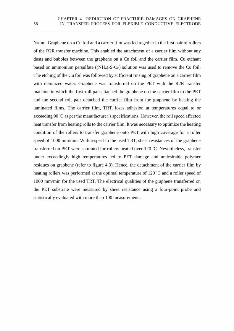
CHAPTER 4 REDUCTION OF FRACTURE DAMAGES ON GRAPHENE
56 IN TRANSFER PROCESS FOR FLEXIBLE CONDUCTIVE ELECTRODE
N/mm. Graphene on a Cu foil and a carrier film was fed together in the first pair of rollers
of the R2R transfer machine. This enabled the attachment of a carrier film without any
dusts and bubbles between the graphene on a Cu foil and the carrier film. Cu etchant
based on ammonium persulfate ((NH4)2S2O8) solution was used to remove the Cu foil.
The etching of the Cu foil was followed by sufficient rinsing of graphene on a carrier film
with deionized water. Graphene was transferred on the PET with the R2R transfer
machine in which the first roll pair attached the graphene on the carrier film to the PET
and the second roll pair detached the carrier film from the graphene by heating the
laminated films. The carrier film, TRT, loses adhesion at temperatures equal to or
exceeding 90 ◦C as per the manufacturer’s specifications. However, the roll speed affected
heat transfer from heating rolls to the carrier film. It was necessary to optimize the heating
condition of the rollers to transfer graphene onto PET with high coverage for a roller
speed of 1000 mm/min. With respect to the used TRT, sheet resistances of the graphene
transferred on PET were saturated for rollers heated over 120 ◦C. Nevertheless, transfer
under exceedingly high temperatures led to PET damage and undesirable polymer
residues on graphene (refer to figure 4.3). Hence, the detachment of the carrier film by
heating rollers was performed at the optimal temperature of 120 ◦C and a roller speed of
1000 mm/min for the used TRT. The electrical qualities of the graphene transferred on
the PET substrate were measured by sheet resistance using a four-point probe and
statistically evaluated with more than 100 measurements.
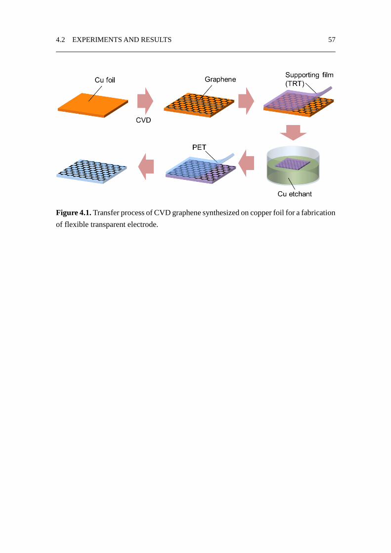
4.2 EXPERIMENTS AND RESULTS 57
Figure 4.1. Transfer process of CVD graphene synthesized on copper foil for a fabrication
of flexible transparent electrode.
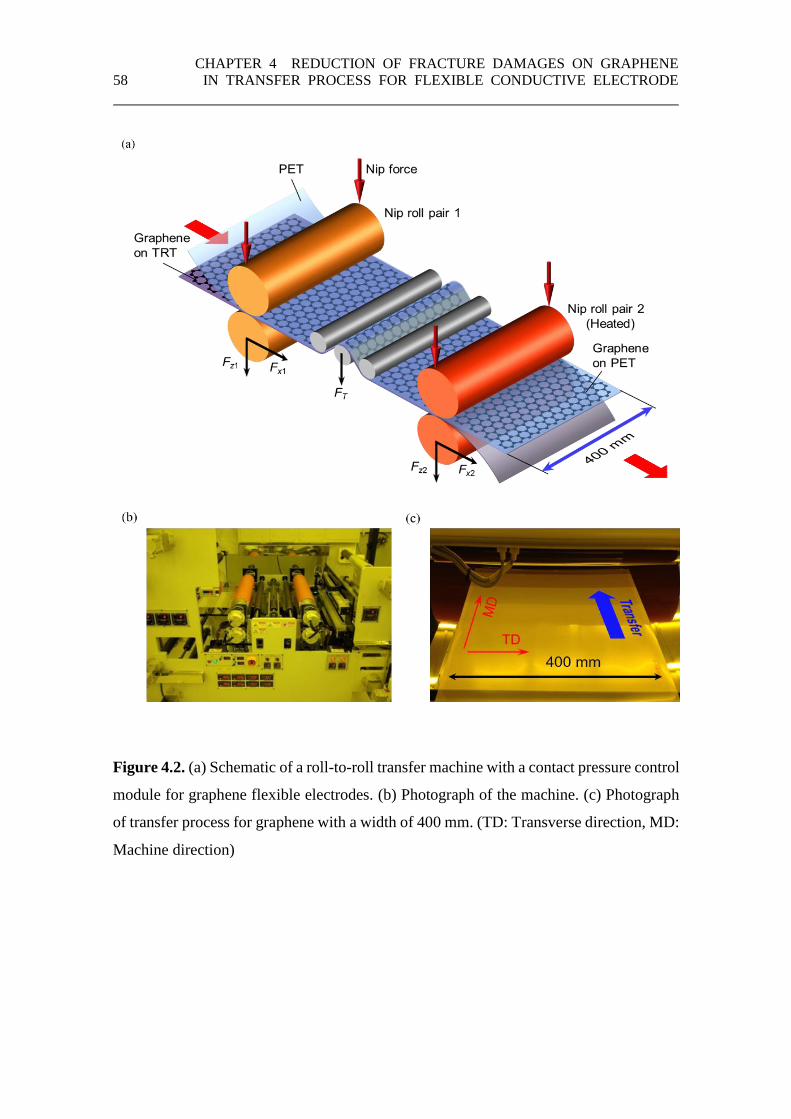
CHAPTER 4 REDUCTION OF FRACTURE DAMAGES ON GRAPHENE
58 IN TRANSFER PROCESS FOR FLEXIBLE CONDUCTIVE ELECTRODE
Figure 4.2. (a) Schematic of a roll-to-roll transfer machine with a contact pressure control
module for graphene flexible electrodes. (b) Photograph of the machine. (c) Photograph
of transfer process for graphene with a width of 400 mm. (TD: Transverse direction, MD:
Machine direction)

4.2 EXPERIMENTS AND RESULTS 59
Figure 4.3. (a) Temperature dependence of sheet resistance of transferred graphene onto
PET substrate. Inset figures are SEM images of TRT surface after transfer. (b) TRT
residues on graphene transferred on PET after transferring with the transfer temperature
of 130 °C, and (c) its corresponding surface morphologies of TRT film after heating.

CHAPTER 4 REDUCTION OF FRACTURE DAMAGES ON GRAPHENE
60 IN TRANSFER PROCESS FOR FLEXIBLE CONDUCTIVE ELECTRODE
4.2.2 Dependence of contact pressure on electrical properties
The effect of a contact pressure induced by the nip rolls on the electrical properties of
graphene was investigated. This was performed by transferring the graphene on the carrier
film to the PET using the roll transfer system displayed in figure 4.2, and various normal
contact forces that were responsible for damage generation during the thin film transfer
process were investigated [20,23,24]. The system consisted of two pairs of rolls with a
diameter of 130 mm each. The upper rolls were coated with a soft rubber with a thickness
of 3.5 mm and Young’s modulus of 6.07 MPa to avoid a contact pressure concentration.
The nip forces (denoted by Fz1, and Fz2) periodically deviated as shown in figure A.2(a)
when the transfer was performed without any feedback control of the contact force. This
is due to machining error of rolls, out-of-roundness of cylinders, non-uniformity in the
thickness of the rubber coating, and misalignment of roll axes. Feedback control modules
were installed in the transfer machine to maintain constant nip forces during the transfer
process as shown in figure A.2(b). Since the disturbances in the shear force and tension
of films fed in the R2R transfer system caused damages, such as cracks, wrinkles, or holes,
to the graphene, it is important to use the integrated force control system to minimize
these disturbances (see Appendix A). After etching the Cu foil with a width of 60 mm,
graphene on the carrier film was transferred onto PET with nip forces per unit width
ranging from 1.63 N/mm to 13.1 N/mm. Electrical quality of the graphene transferred on
the PET was evaluated in terms of sheet resistance for the entire transferred area. Figure
4.4(a) shows the dependence of contact load per unit width of the graphene on the sheet
resistance of the graphene transferred on the PET.
The finite element method (FEM) was used to obtain maximum contact pressure in
the R2R transfer process for quantitative analyses purposes. The finite element model
involved compressing the laminated structure composed of the carrier film, graphene, and
PET by two rolls with the rubber coating. The maximum pressure caused by the rolling
contacts can be approximated by that from the compression of the static rolls under the
assumption of the quasi-static process. Hence, the relationship calculated by the FEM
indicated that the nip force was correlated with the maximum pressure during the R2R
transfer process. The average sheet resistance measured in the graphene transferred with
high contact pressure was higher than that in the graphene transferred with low contact

4.2 EXPERIMENTS AND RESULTS 61
pressure. Additionally, the standard deviation also increased when transfer was performed
with high contact pressure. This indicated that the localized damages, which deteriorated
the electrical qualities of graphene, were generated during the graphene transfer process
with high contact pressure.

CHAPTER 4 REDUCTION OF FRACTURE DAMAGES ON GRAPHENE
62 IN TRANSFER PROCESS FOR FLEXIBLE CONDUCTIVE ELECTRODE
Figure 4.4. (a) Sheet resistance of the graphene transferred on a PET substrate with
various nip forces. (b) Relationship between nip forces per unit width and maximum
contact pressure applied by nip rolls with a diameter of 130 mm.
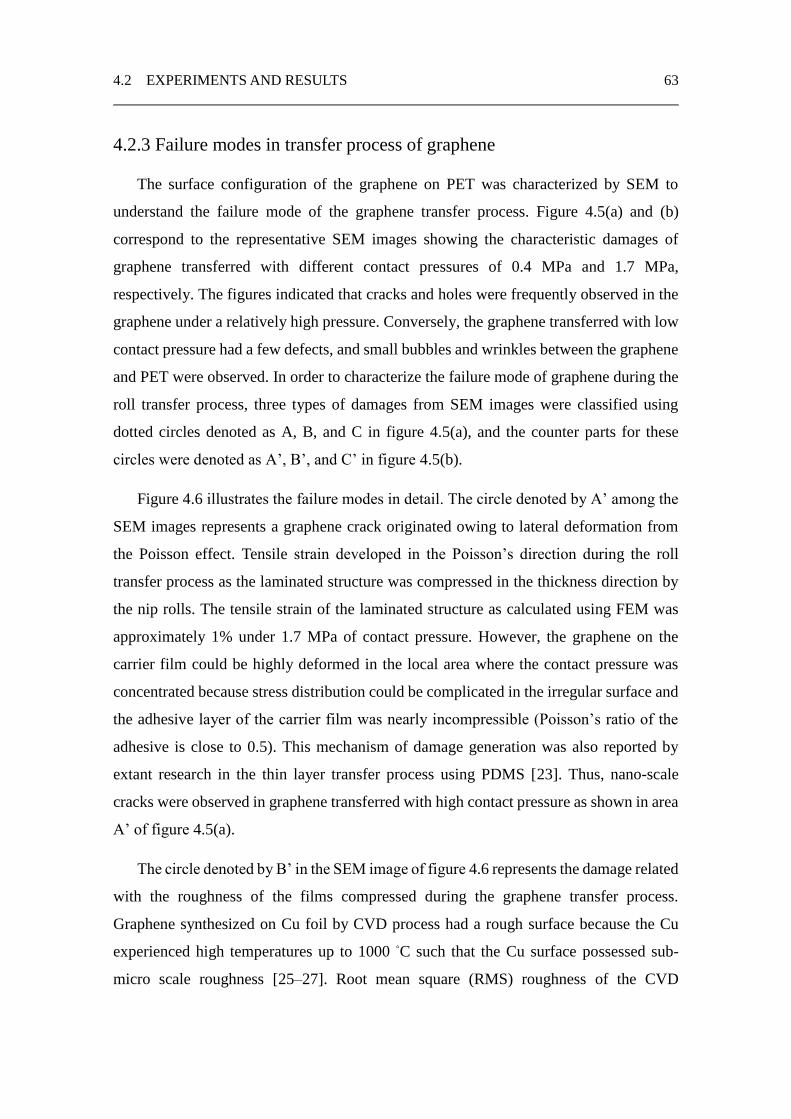
4.2 EXPERIMENTS AND RESULTS 63
4.2.3 Failure modes in transfer process of graphene
The surface configuration of the graphene on PET was characterized by SEM to
understand the failure mode of the graphene transfer process. Figure 4.5(a) and (b)
correspond to the representative SEM images showing the characteristic damages of
graphene transferred with different contact pressures of 0.4 MPa and 1.7 MPa,
respectively. The figures indicated that cracks and holes were frequently observed in the
graphene under a relatively high pressure. Conversely, the graphene transferred with low
contact pressure had a few defects, and small bubbles and wrinkles between the graphene
and PET were observed. In order to characterize the failure mode of graphene during the
roll transfer process, three types of damages from SEM images were classified using
dotted circles denoted as A, B, and C in figure 4.5(a), and the counter parts for these
circles were denoted as A’, B’, and C’ in figure 4.5(b).
Figure 4.6 illustrates the failure modes in detail. The circle denoted by A’ among the
SEM images represents a graphene crack originated owing to lateral deformation from
the Poisson effect. Tensile strain developed in the Poisson’s direction during the roll
transfer process as the laminated structure was compressed in the thickness direction by
the nip rolls. The tensile strain of the laminated structure as calculated using FEM was
approximately 1% under 1.7 MPa of contact pressure. However, the graphene on the
carrier film could be highly deformed in the local area where the contact pressure was
concentrated because stress distribution could be complicated in the irregular surface and
the adhesive layer of the carrier film was nearly incompressible (Poisson’s ratio of the
adhesive is close to 0.5). This mechanism of damage generation was also reported by
extant research in the thin layer transfer process using PDMS [23]. Thus, nano-scale
cracks were observed in graphene transferred with high contact pressure as shown in area
A’ of figure 4.5(a).
The circle denoted by B’ in the SEM image of figure 4.6 represents the damage related
with the roughness of the films compressed during the graphene transfer process.
Graphene synthesized on Cu foil by CVD process had a rough surface because the Cu
experienced high temperatures up to 1000 ◦C such that the Cu surface possessed sub-
micro scale roughness [25–27]. Root mean square (RMS) roughness of the CVD
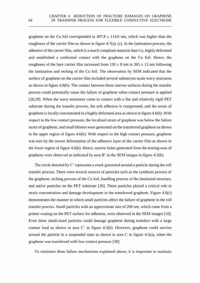
CHAPTER 4 REDUCTION OF FRACTURE DAMAGES ON GRAPHENE
64 IN TRANSFER PROCESS FOR FLEXIBLE CONDUCTIVE ELECTRODE
graphene on the Cu foil corresponded to 497.8 ± 114.6 nm, which was higher than the
roughness of the carrier film as shown in figure 4.7(a), (c). In the lamination process, the
adhesive of the carrier film, which is a much compliant material than Cu, highly deformed
and established a conformal contact with the graphene on the Cu foil. Hence, the
roughness of the bare carrier film increased from 150 ± 8 nm to 365 ± 13 nm following
the lamination and etching of the Cu foil. The observation by SEM indicated that the
surface of graphene on the carrier film included several submicron-scale wavy structures
as shown in figure 4.8(b). The contact between these uneven surfaces during the transfer
process could potentially cause the failure of graphene when contact pressure is applied
[28,29]. When the wavy structures come in contact with a flat and relatively rigid PET
substrate during the transfer process, the soft adhesive is compressed, and the strain of
graphene is locally concentrated in a highly deformed area as shown in figure 4.6(b). With
respect to the low contact pressure, the localized strain of graphene was below the failure
strain of graphene, and small blisters were generated on the transferred graphene as shown
in the upper region of figure 4.6(b). With respect to the high contact pressure, graphene
was torn by the severe deformation of the adhesive layer of the carrier film as shown in
the lower region of figure 4.6(b). Hence, narrow holes generated from the tearing-outs of
graphene were observed as indicated by area B’ in the SEM images in figure 4.5(b).
The circle denoted by C’ represents a crack generated around a particle during the roll
transfer process. There were several sources of particles such as the synthesis process of
the graphene, etching process of the Cu foil, handling process of the laminated structure,
and native particles on the PET substrate [26]. These particles played a critical role in
strain concentration and damage development in the transferred graphene. Figure 4.6(c)
demonstrates the manner in which small particles affect the failure of graphene in the roll
transfer process. Small particles with an approximate size of 200 nm, which came from a
primer coating on the PET surface for adhesion, were observed in the SEM images [10].
Even these small-sized particles could damage graphene during transfers with a large
contact load as shown in area C’ in figure 4.5(b). However, graphene could survive
around the particle in a suspended state as shown in area C in figure 4.5(a), when the
graphene was transferred with low contact pressure [30].
To minimize three failure mechanisms explained above, it is important to maintain
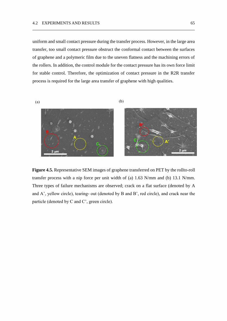
4.2 EXPERIMENTS AND RESULTS 65
uniform and small contact pressure during the transfer process. However, in the large area
transfer, too small contact pressure obstruct the conformal contact between the surfaces
of graphene and a polymeric film due to the uneven flatness and the machining errors of
the rollers. In addition, the control module for the contact pressure has its own force limit
for stable control. Therefore, the optimization of contact pressure in the R2R transfer
process is required for the large area transfer of graphene with high qualities.
Figure 4.5. Representative SEM images of graphene transferred on PET by the rollto-roll
transfer process with a nip force per unit width of (a) 1.63 N/mm and (b) 13.1 N/mm.
Three types of failure mechanisms are observed; crack on a flat surface (denoted by A
and A’, yellow circle), tearing- out (denoted by B and B’, red circle), and crack near the
particle (denoted by C and C’, green circle).
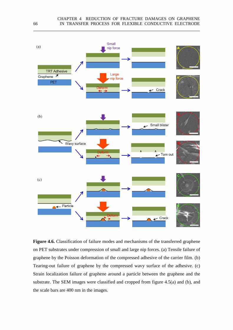
CHAPTER 4 REDUCTION OF FRACTURE DAMAGES ON GRAPHENE
66 IN TRANSFER PROCESS FOR FLEXIBLE CONDUCTIVE ELECTRODE
Figure 4.6. Classification of failure modes and mechanisms of the transferred graphene
on PET substrates under compression of small and large nip forces. (a) Tensile failure of
graphene by the Poisson deformation of the compressed adhesive of the carrier film. (b)
Tearing-out failure of graphene by the compressed wavy surface of the adhesive. (c)
Strain localization failure of graphene around a particle between the graphene and the
substrate. The SEM images were classified and cropped from figure 4.5(a) and (b), and
the scale bars are 400 nm in the images.
4.2 EXPERIMENTS AND RESULTS 67
Figure 4.7. Roughness measurement results by white light interferometry for graphene
on Cu foils, carrier films (TRT), graphene on the carrier films, and substrates (PET). (a),
(b) 3D surface morphologies of each film (300 µm × 200 µm). (c) RMS roughness of each
surface.

CHAPTER 4 REDUCTION OF FRACTURE DAMAGES ON GRAPHENE
68 IN TRANSFER PROCESS FOR FLEXIBLE CONDUCTIVE ELECTRODE
Figure 4.8. Rotational synchronization of nip rolls. (a) Schematics of synchronization
test. (b) Sheet resistance changes of the example case with synchronized setting and
different velocity setting of upper and lower roll. (c) Parallel wrinkles of graphene
transferred on PET, which is observed in extreme case of asynchronous rotation velocity.
(d) Warpage of TRT/graphene/PET structure laminated without synchronization of
rotational velocity.

4.2 EXPERIMENTS AND RESULTS 69
4.2.4 Numerical simulation
To analyze the effect of wavy structures and particles on the graphene damages, FEM
was adopted to simulate the stress and strain distributions of the compressed layers during
the transfer process. Figure 4.9 illustrates a simulated model with FEM. The adhesive
layer of a carrier film played a key role in the deformation of graphene during the transfer
process. The thickness of the adhesive layer was 60 µm, and its surface tightly adhered to
the graphene. The wavy structures of the adhesive layer in contact with the flat PET
surface are shown in figure 4.9(a), where the wavelength and amplitude were modeled as
2 µm and 360 nm, respectively, by analyzing the SEM image in figure 4.10(b). Figure
4.9(b) describes the model for a contact between a flat TRT adhesive and a 200 nm-sized
hemisphere attached on a flat PET surface. Because the elastic modulus of PET is a
hundred thousand times higher than that of the adhesive, it was modeled as a rigid surface.
The mechanical properties of the materials used for simulation models are listed in Table
1. Young’s modulus of graphene is estimated by analytic calculation and experiments
[2,31]. And, Young’s modulus of TRT adhesive is assumed as a modulus measured by
tensile test for conventional adhesive layer, which is similar types of TRT adhesive [32].
Also, the properties of PET and rubber coating of the rollers are measured by uniaxial
tensile test and hardness test, respectively. Numerical simulations were performed using
a commercial FEM solver, ABAQUS. Two dimensional plane strain elements were
adopted for the contact between a wavy adhesive and a flat PET while axisymmetric
elements were used for the contact between a flat surface and a particle.
Figure 4.9(a) shows the evolution of deformation for graphene attached on the wavy
surface of the adhesive from an initial contact to a severely compressed state. When the
wavy surface of the adhesive came in contact with the flat substrate, the wavy structure
began to collapse, and the contact area between the graphene and the substrate increased
as the compression load increased. The adhesive surface holding the graphene deformed
like a deep valley and experienced highly localized stress and strain. Note that this
deformed shape was completely different from that of the wavy adhesive surface without
any graphene layer (see Appendix B and figure B.1). This highly localized strain of the
adhesive near the valley-like structure could trigger the fracture of the graphene during
the transfer process.

CHAPTER 4 REDUCTION OF FRACTURE DAMAGES ON GRAPHENE
70 IN TRANSFER PROCESS FOR FLEXIBLE CONDUCTIVE ELECTRODE
When a hemispheric particle indented the graphene on the adhesive, a large deformed
region of the adhesive was in close proximity with the top end of the particle as shown in
figure 4.9(b). The fracture of graphene on the top of the particles was experimentally
observed in both figure 4.5(a) and (b), where small white rings indicate that the graphene
is fractured and collapsed near the particles. When the graphene comes in contact with
and sticks to the surface of the particle, the graphene on the adhesive could not undergo
large deformation due to the constraint of the adhesion between the graphene and the
particle. Based on this mechanics, the graphene in area C of figure 4.5(a) were transferred
on the particle without damages by applying low contact pressure. On the other hand,
under high contact pressure, the strain could be accumulated along the suspended region,
not along the top region of the particle because the suspended region has no constraint of
the adhesion between the graphene and the particle. This leaded to the fracture near the
suspended region of the graphene under high pressure as shown in area C’ of figure 4.5(b).
Table 1. Young’s modulus and Poisson’s ratio of each material used in the analysis
Young’s modulus Poisson’s ratio
Graphene 1.0 TPa 0.165
PET 2.0 GPa 0.4
Rubber coating 6.06 MPa 0.5
TRT adhesive 20 kPa 0.5

4.2 EXPERIMENTS AND RESULTS 71
Figure 4.9. Deformation and principal strain distributions of a carrier film adhesive reveal
the failure mechanisms of graphene during the transfer process. (a) Contact between the
graphene on a wavy carrier film surface and a flat substrate. (b) Contact between the
graphene on a flat carrier film and a substrate with a particle.
Figure 4.10. SEM images of (a) graphene on Cu foil and (b) graphene on the carrier film
(TRT).
CHAPTER 4 REDUCTION OF FRACTURE DAMAGES ON GRAPHENE
72 IN TRANSFER PROCESS FOR FLEXIBLE CONDUCTIVE ELECTRODE
4.2.5 Large area transfer of graphene
For large area transfer of graphene with minimized mechanical damages, the localized
high contact pressure should be avoided as discussed in the previous sections. In addition
to the contact pressure control, an R2R machine has a function of tension control and
roller synchronization to realize continuous manufacturing, and an integrated R2R
machine with these functions and contact pressure control is described in supporting
information S4. The carrier film and the flexible substrate undergo tension during the
continuous R2R process, and this tension can lead to the tensile failure of graphene in a
manner similar to the first mechanism. A relative speed mismatch in the motion between
the two contacted pairs of rollers leads to shear traction on the transferred graphene, and
this can wear out the graphene due to the application of shear traction on the graphene.
The developed R2R transfer machine was designed by considering the contact pressure
control, tension control, and the synchronization controls as described in figure A.1. The
use of the R2R transfer machine as shown in figure 4.2(b) and (c) can minimize the
activation of the three failure mechanisms by applying optimized and uniform contact
pressure not to damage the graphene (previously discussed in section 4.2.3) during the
transfer process.
The continuous roll transfer process produced large scale graphene electrodes with a
width of 400 mm. The movie in the supporting information shows the R2R transfer
process of graphene. Following the transfer process, the distribution of sheet resistance
was obtained by mapping the graphene electrode with a four-point probe. Figure 4.7(a)
and (c) show the maps and the histograms of the sheet resistance of graphene transferred
using the R2R transfer system at a speed of 1000 mm/min. For comparison purposes, a
conventional lamination system without the contact pressure control module was used to
transfer graphene of the same size, and the electrical qualities are demonstrated in figure
4.7(b) and (c) [5]. As observed, the area corresponding to the transferred graphene
indicated several regions with poor electrical qualities. This was attributed to the non-
uniform contact pressure and unintended shear force that induced wrinkles and damages
in the graphene. However, the uniform contact pressure established by the pressure
controlled R2R transfer machine led to the excellent electrical performance of the
graphene transferred to the PET. Additionally, the optimized contact pressure could

4.2 EXPERIMENTS AND RESULTS 73
minimize damages on the graphene, and improve the uniformity as well as the average
values of the sheet resistance of the graphene film. These results are also consistent with
the contact pressure-dependent sheet resistance data shown in figure 4.4(a), and
confirmed that concentrated contact pressure degrades the electrical conductivity and its
uniformity of the transferred graphene.
Figure 4.7. Sheet resistance results of the graphene electrodes transferred on flexible PET
substrates. (a, b) Sheet resistance maps, and (c, d) histograms for the transferred graphene
electrodes (size: 400 mm (TD) × 300 mm (MD)). (a, c) Transfer with a feedback-
controlled nip force per unit width of 0.5 N/mm, and (b, d) transfer without nip force
control.
4.3 CONCLUSIONS 74
4.3 Conclusion
In this chapter, a damage mitigation method for the roll transfer process of graphene
was developed. To investigate the failure modes and the corresponding failure
mechanisms during the transfer process, different contact pressure levels were examined
to transfer CVD-grown graphene on PET, and the results were compared in terms of the
electrical quality after the transfer. The mechanical damages generated by high contact
pressure were identified and classified based on SEM images and the electrical properties
of the transferred graphene. Finite element analysis was used to discuss and analyze the
three types of failure mechanisms induced by high contact pressure. The rough surfaces
of graphene on a carrier film and undesirable particles were attributed to the main causes
for the mechanical damages of the transferred graphene. Finally, a large area transfer of
graphene with a 400 mm width was realized at a transfer speed of 1000 mm/min for
transparent conductive films with excellent electrical qualities. This demonstrates the
scalability and high productivity of the developed R2R transfer technology.
For the application of graphene, CVD graphene is promising due to its scalability and
high qualities. However, many defects such as holes, foldings, wrinkles, and tearings
could be a hurdles in the manufacturing process and the reliability of final products due
to its brittle nature. Understanding of fracture mechanics of graphene is crucial for the
application of graphene. Hence, the fracture mechanics researches of graphene should be
emphasize on the development of various graphene-based devices.
REFERENCES 75
References
[1] K.S. Novoselov, A.K. Geim, S.V. Morozov, D. Jiang, Y. Zhang, S.V. Dubonos, I.V.
Grigorieva, A.A. Firsov, Electric field effect in atomically thin carbon films. Science
306 (2004) 666-669.
[2] C. Lee, X. Wei, J.W. Kysar, J. Hone, Measurement of the elastic properties and
intrinsic strength of monolayer graphene, Science 321 (2008) 385-388.
[3] X. Li, Y. Zhu, W. Cai, M. Borysiak, B. Han, D. Chen, R.D. Piner, L. Colombo, R.S.
Ruoff, Transfer of large-area graphene films for high-performance transparent
conductive electrodes, Nano Lett. 9 (2009) 4359–4363.
[4] X. Wang, L. Zhi, K. Müllen, Transparent, conductive graphene electrodes for dye-
sensitized solar cells, Nano Lett. 8 (2008) 323–327.
[5] S. Bae, H. Kim, Y. Lee, X. Xu, J.-S. Park, Y. Zheng, J. Balakrishnan, T. Lei, H.R.
Kim, Y.I. Song, Y.-J. Kim, K.S. Kim, B. Ö zyilmaz, J.-H. Ahn, B.H. Hong, S. Iijima,
Roll-to-roll production of 30-inch graphene films for transparent electrodes, Nat.
Nanotechnol. 5 (2010) 574–578.
[6] J. Ryu, Y. Kim, D. Won, N. Kim, J.S. Park, E.-K. Lee, D. Cho, S.-P. Cho, S.J. Kim,
G.H. Ryu, H.-A.-S. Shin, Z. Lee, B.H. Hong, S. Cho, Fast synthesis of high-
performance graphene films by hydrogen-free rapid thermal chemical vapor
deposition, ACS Nano 8 (2014) 950–956.
[7] K.S. Kim, Y. Zhao, H. Jang, S.Y. Lee, J.M. Kim, K.S. Kim, J.-H. Ahn, P. Kim, J.-Y.
Choi, B.H. Hong, Large-scale pattern growth of graphene films for stretchable
transparent electrodes, Nature 457 (2009) 706–710.

CHAPTER 4 REDUCTION OF FRACTURE DAMAGES ON GRAPHENE
76 IN TRANSFER PROCESS FOR FLEXIBLE CONDUCTIVE ELECTRODE
[8] T. Kobayashi, M. Bando, N. Kimura, K. Shimizu, K. Kadono, N. Umezu, K. Miyahara,
S. Hayazaki, S. Nagai, Y. Mizuguchi, Y. Murakami, D. Hobara, Production of a 100-
m-long high-quality graphene transparent conductive film by roll-to-roll chemical
vapor deposition and transfer process, Appl. Phys. Lett. 102 (2013) 023112.
[9] A. Zurutuza, C. Marinelli, Challenges and opportunities in graphene
commercialization, Nature Nanotech. 9 (2014) 730-734.
[10] S. Won, Y. Hwango, S.-K. Lee, K.-S. Kim, K.-S. Kim, S.-M. Lee, H.-J. Lee, J.-H.
Ahn, J.-H. Kim, S.-B. Lee, Double-layer CVD graphene as stretchable transparent
electrodes, Nanoscale 6 (2014) 6057-6064.
[11] Q. Yu, J. Lian, S. Siriponglert, H. Li, Y.P. Chen, S.S. Pei, Graphene segregated on
Ni surfaces and transferred to insulators, Appl. Phys. Lett. 93 (2008) 113103.
[12] X. Li, W. Cai, J. An, S. Kim, J. Nah, D. Yang, R. Piner, A. Velamakanni, I. Jung, E.
Tutuc, S.K. Banerjee, L. Colombo, R.S. Ruoff, Large-area synthesis of high-quality
and uniform graphene films on copper foils, Science 324 (2009) 1312–1314.
[13] C. Berger, Z. Song, T. Li, X. Li, A.Y. Ogbazghi, R. Feng, Z. Dai, A.N. Marchenkov,
E.H. Conrad, P.N. First, W.A. de Heer, Ultrathin epitaxial graphite: 2D electron gas
properties and a route toward graphene-based nanoelectronics J. Phys. Chem. B 108
(2004) 19912–19916.
[14] X.-D. Chen, Z.-B. Liu, C.-Y. Zheng, F. Xing, X.-Q. Yan, Y. Chen, J.-G. Tian, High-
quality and efficient transfer of large-area graphene films onto different substrates,
Carbon 56 (2013) 271–278.
[15] J. Song, F.-Y. Kam, R.-Q. Png, W.-L. Seah, J.-M. Zhuo, G.-K. Lim, P.K.H. Ho, L.-
L. Chua, A general method for transferring graphene onto soft surfaces, Nat.
Nanotechnol. 8 (2013) 356–362.
[16] B.N. Chandrashekar, B. Deng, A.S. Smitha, Y. Chen, C. Tan, H. Zhang, H. Peng, Z.
Liu, Roll-to-roll green transfer of CVD graphene onto plastic for a transparent and
flexible triboelectric nanogenerator, Adv. Mater. 27 (2015) 5210–5216.
[17] L.G. Martins, Y. Song, T. Zeng, M.S. Dresselhaus, J. Kong, P.T. Araujo, Direct
transfer of graphene onto flexible substrates, Proc. Natl. Acad. Sci. 110 (2013)
17762–17767.
REFERENCES 77
[18] G.J.M. Fechine, I. Martin-Fernandez, G. Yiapanis, R. Bentini, E.S. Kulkarni, R.V.B.
de Oliveira, X. Hu, I. Yarovsky, A.H.C. Neto, B. Ö zyilmaz, Direct dry transfer of
chemical vapor deposition ̈graphene to polymeric substrates, Carbon 83 (2015) 224–
231.
[19] T. Choi, S.J. Kim, S. Park, T.Y. Hwang, Y. Jeon, B.H. Hong, Roll-to-roll continuous
patterning and transfer of graphene via dispersive adhesion, Nanoscale 7 (2015)
7138–7142.
[20] J. Kang, S. Hwang, J.H. Kim, M.H. Kim, J. Ryu, S.J. Seo, B.H. Hong, M.K. Kim,
J.-B. Choi, Efficient transfer of large-area graphene films onto rigid substrates by hot
pressing, ACS Nano 6 (2012) 5591–5598.
[21] S.R. Na, X. Wang, R.D. Piner, R. Huang, C.G. Willson, K.M. Liechti, Cracking of
polycrystalline graphene on copper under tension, ACS nano 10 (2016) 9616–9625.
[22] J.R. Weertman, Hall-Petch strengthening in nanocrystalline metals, Mater. Sci. Eng.
A 166 (1993) 161–167.
[23] B.K. Sharma, B. Jang, J.E. Lee, S.-H. Bae, T.W. Kim, H.-J. Lee, J.-H. Kim, J.-H.
Ahn, Load-controlled roll transfer of oxide transistors for stretchable electronics, Adv.
Funct. Mater. 23 (2013) 2024–2032.
[24] T.A. Stolarski, S. Tobe, Rolling Contacts. (Professional Engineering Publishing
Limited, London, 2000).
[25] P. Procházka, J. Mach, D. Bischoff, Z. Lišková, P. Dvořák, M. Vaňatka, P. Simonet,
A. Varlet, D. Hemzal, M. Petrenec, Ultrasmooth metallic foils for growth of high
quality graphene by chemical vapor deposition, Nanotechnology 25 (2014) 185601.
[26] S.-M. Kim, J.-H. Kim, K.-S. Kim, Y. Hwangbo, J.-H. Yoon, E.-K. Lee, J. Ryu, H.-
J. Lee, S. Cho, S.-M. Lee, Synthesis of CVD-graphene on rapidly heated copper foils,
Nanoscale 6 (2014) 4728–4734.
[27] N. Liu, Z. Pan, L. Fu, C. Zhang, B. Dai, Z. Liu, The origin of wrinkles on transferred
graphene, Nano Res. 4 (2011) 996–1004.
[28] M.H. Griep, E. Sandoz-Rosado, T.M. Tumlin, E. Wetzel, Enhanced graphene
mechanical properties through ultrasmooth copper growth substrates, Nano Lett. 16
(2016) 1657–1662.
CHAPTER 4 REDUCTION OF FRACTURE DAMAGES ON GRAPHENE
78 IN TRANSFER PROCESS FOR FLEXIBLE CONDUCTIVE ELECTRODE
[29] J.-Y. Hong, Y.C. Shin, A. Zubair, Y. Mao, T. Palacios, M.S. Dresselhaus, S.H. Kim,
J. Kong, A rational strategy for graphene transfer on substrates with rough features,
Adv. Mater. 28 (2016) 2382–2392.
[30] Z. Zong, C.-L. Chen, M.R. Dokmeci, K. Wan, Direct measurement of graphene
adhesion on silicon surface by intercalation of nanoparticles J. Appl. Phys. 107 (2010)
026104.
[31] L. Zhou, Y. Wang, G. Cao, Elastic properties of monolayer graphene with different
chiralities, J. Phys.: Condens. Matter. 25 (2013) 125302.
[32] A. Murata, T. Oshima, Y. Arimitsu, K. Kiuchi, Heat-peelable pressure-sensitive
adhesive sheet, US Patent 7,718,257 (2010)
APPENDIX A 79
Appendix A
Figure A.1 shows a force diagram of the roll transfer system integrated with the force
control module. Films are continuously fed from the left side and pass through the first
nip rolls, tension control module, and the second nip rolls, step by step. Each roll pair
composed of a master roll (upper side) and a slave roll (bottom side). The axis of the
master roll is fixed, but the axis of the slave roll is connected with the translation stage in
vertical direction to control nip force uniformly by the load cells to measure the force of
normal directions. The load cells to measure the force of lateral directions, equipped in
the axis of the slave roll, can detect shear forces applied to the films. For convenience,
the index of the first master roll, the first slave roll, the second master roll, and the second
slave roll is referred as M1, S1, M2, and S2, respectively. When the system is stably
controlled, the linear velocity is expressed as, v = R, where R is a radius of rolls, and
is an angular velocity of rolls. Here, it is possible to define average linear velocity and
relative linear velocity for each nip roll like,
�̅�1,2 =𝑣𝑀1,2 + 𝑣𝑆1,2
2=
𝑅
2(𝜔𝑀1,2 + 𝜔𝑆1,2),
∆𝑣1,2 = 𝑣𝑀1,2 − 𝑣𝑆1,2 = 𝑅(𝜔𝑀1,2 − 𝜔𝑆1,2).
To establish a stable operation, tension is applied films fed to the system. Since nip rolls
isolate tensions, it is possible to consider the three tension values in the system, T1, T2,
and T3. T2 is directly measured with a tension load cell installed in the tension control
module with the relation of 𝐹𝑇 = 2𝑇2sin𝜃. If the shear force applied between nip rolls is
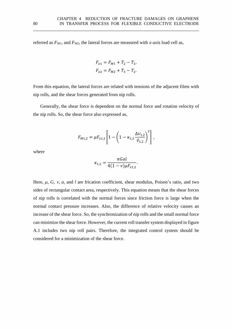
CHAPTER 4 REDUCTION OF FRACTURE DAMAGES ON GRAPHENE
80 IN TRANSFER PROCESS FOR FLEXIBLE CONDUCTIVE ELECTRODE
referred as FM1, and FM2, the lateral forces are measured with x-axis load cell as,
𝐹𝑥1 = 𝐹𝑀1 + 𝑇2 − 𝑇1,
𝐹𝑥2 = 𝐹𝑀2 + 𝑇3 − 𝑇2.
From this equation, the lateral forces are related with tensions of the adjacent films with
nip rolls, and the shear forces generated from nip rolls.
Generally, the shear force is dependent on the normal force and rotation velocity of
the nip rolls. So, the shear force also expressed as,
𝐹𝑀1,2 = 𝜇𝐹𝑧1,2 [1 − (1 − 𝜅1,2
Δ𝑣1,2
�̅�1,2)
2
] ,
where
𝜅1,2 =𝜋𝐺𝑎𝑙
4(1 − 𝜈)𝜇𝐹𝑧1,2.
Here, , G, , a, and l are frication coefficient, shear modulus, Poison’s ratio, and two
sides of rectangular contact area, respectively. This equation means that the shear forces
of nip rolls is correlated with the normal forces since friction force is large when the
normal contact pressure increases. Also, the difference of relative velocity causes an
increase of the shear force. So, the synchronization of nip rolls and the small normal force
can minimize the shear force. However, the current roll transfer system displayed in figure
A.1 includes two nip roll pairs. Therefore, the integrated control system should be
considered for a minimization of the shear force.
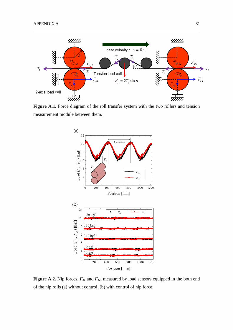
APPENDIX A 81
Figure A.1. Force diagram of the roll transfer system with the two rollers and tension
measurement module between them.
Figure A.2. Nip forces, Fz1 and Fz2, measured by load sensors equipped in the both end
of the nip rolls (a) without control, (b) with control of nip force.
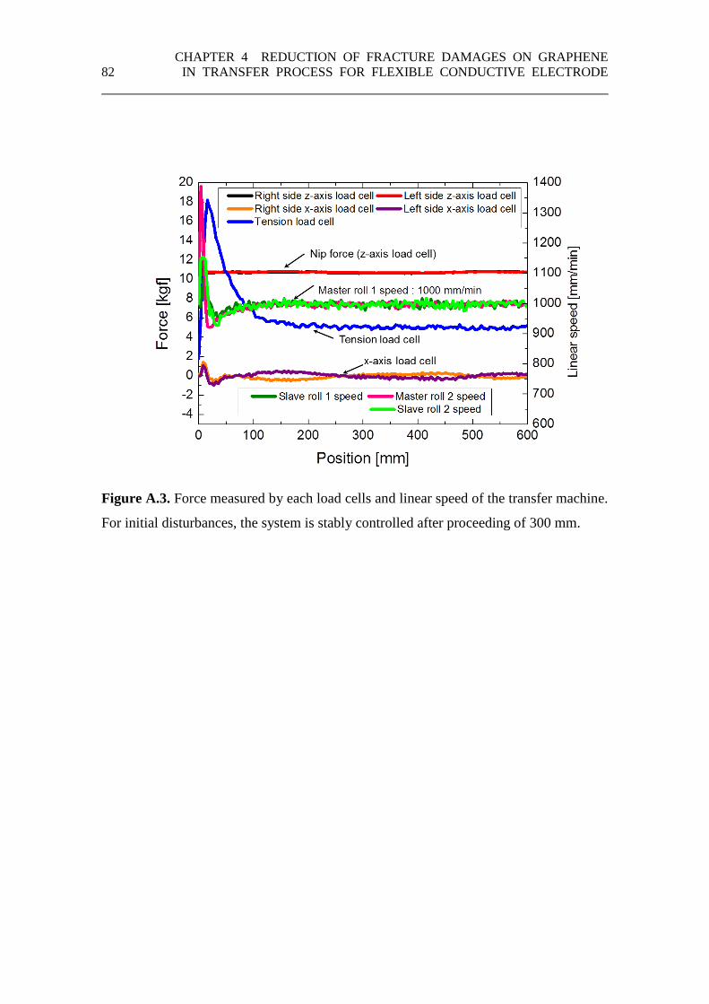
CHAPTER 4 REDUCTION OF FRACTURE DAMAGES ON GRAPHENE
82 IN TRANSFER PROCESS FOR FLEXIBLE CONDUCTIVE ELECTRODE
Figure A.3. Force measured by each load cells and linear speed of the transfer machine.
For initial disturbances, the system is stably controlled after proceeding of 300 mm.
APPENDIX B 83
Appendix B
To investigate deformations of adhesive in a carrier film during the transfer process,
finite element analysis is performed using commercial finite element method code,
ABAQUS. The adhesive layer with 60 μm thickness and wavy surface is compressed on
the flat and rigid substrate.
Figure B.1 illustrates maximum principal strain distribution of the adhesive layer.
The adhesive layer without graphene layer deform and the contact region of it increase
under compression as shown figure B.1(b). Before fully contact state, δ = 180 nm, the
crest start to contact to the substrate and the adhesive largely deforms near it. After entire
surface of the adhesive fully contact with the substrate at δ = 182 nm, strain near the
surface is under 0.1. In addition, the wavy surface of the adhesive establish a conformal
contact with the flat surface. This result can explain the reason why the roughness of bare
TRT increase after lamination with graphene on Cu foil, and etching of Cu foil. When it
comes to contact between rough and rigid graphene on Cu, and relatively flat TRT, the
adhesive of TRT largely deforms viscoplastically and conform the surface of the graphene.
After etching of Cu, the surface of graphene on TRT resembles the surface of graphene
on Cu foil.
However, when thin and stiff graphene layer is covered on the wavy surface of the
adhesive layer, the adhesive layer largely deform in local area compared to the surface
without graphene, as shown in figure B.1(a). This is because the buckling of graphene
layer on the adhesive under the compression. Because of the mismatch of the modulus
between the adhesive and the graphene, relatively stiff graphene layer is buckled. Even
though, high normal stress is applied on the adhesive, the surface cannot fully contact
with the flat substrate. This buckling mechanism can explain the damage induced by

CHAPTER 4 REDUCTION OF FRACTURE DAMAGES ON GRAPHENE
84 IN TRANSFER PROCESS FOR FLEXIBLE CONDUCTIVE ELECTRODE
normal stress in the wavy structure of the adhesive.

APPENDIX A 85
Figure B.1. Strain distribution of an adhesive layer of a carrier film used in graphene
transfer, with respect to displacements. (a) Wavy-structured adhesive layer with graphene
layer, and (b) wavy structured adhesive layer without graphene layer.

CHAPTER 4 REDUCTION OF FRACTURE DAMAGES ON GRAPHENE
86 IN TRANSFER PROCESS FOR FLEXIBLE CONDUCTIVE ELECTRODE

87
Chapter 5
Conclusion
In this thesis, in situ fracture testing method under SEM for atomically thin graphene
was developed. Using this method, fracture behavior of multilayer graphene was
developed and toughening mechanisms of multilayer graphene are investigated. In
addition, the fabrication process of graphene transparent conductive film for a mass
production based on the knowledges to fracture characteristics of graphene was proposed.
In chapter 2, a methodology for measuring the fracture behavior of freestanding
graphene using an in situ tensile tester under SEM was proposed. To fabricate a
freestanding specimen of atomically thin graphene, pristine graphene exfoliated from
natural graphite was transferred on the accurate position of the tensile device with
polymer layer to protect from damages. A pre-crack was introduced on a freestanding
graphene specimen using focused ion beam. Utilizing the advantages of the in situ
fracture test, load–displacement data of single-crystalline bilayer graphene was measured
and a fracture behavior during the crack extension along its zig-zag direction was
observed in in situ SEM images. Young’s modulus and the stress field of the specimen at
the moment of fracture were evaluated from the measured data and finite element analysis.
In chapter 3, fracture behavior of multilayer graphene was investigated using an in
situ mode I fracture test under a scanning electron microscope. The fracture toughness of
the graphene was determined from measured load-displacement curves and finite element
analysis. Nonlinear elastic fracture behavior of the multilayer graphene is discussed based
88 CHAPTER 7 CONCLUSION
on nonlinear elastic fracture mechanics. In situ SEM images obtained during the fracture
test showed asynchronous crack propagation with independent path, causing interlayer
shear stress and slippages. In addition, it was found that interlayer slippages between the
graphene layers are the reason for the enhanced fracture toughness of multilayer graphene.
In chapter 4, a damage mitigation method for the roll transfer process of graphene
was investigated. Sheet resistance of graphene transparent electrode transferred with
different contact pressure explain that high contact pressure causes the mechanical
damages of transferred graphene. By analyzing SEM images of the damages on the
transferred graphene, three types of failure modes were classified, and the corresponding
failure mechanisms were revealed using the surface morphology and the finite element
analyses. Based on the understanding of the failure mechanisms, the graphene transfer
with a width of 400 mm was realized at a speed of 1000 mm/min using an R2R transfer
machine with the capability of nip force control.
Graphene, thin carbon materials with atomic thickness, is fascinating materials to
extend research area of fracture mechanics. As many of research issues are still remained
in this area, I expect that the fracture mechanics of two dimensional materials will be
established, in the near future. At a viewpoint of the applications of graphene, I would
like to propose several fracture mechanics topics of graphene. The first is effects of
defects on fracture behaviors of graphene. In this thesis, I mainly focused on the fracture
characteristics of pristine graphene, which is single crystal and possesses few atomic
disorders. However, there are many kinds of defects such as grain boundary, atomic
vacancy defect, overlapping domain boundary, and various topological defects. The
effects of various defects on fracture characteristics of graphene need to be elucidated,
because the generation of such defects are inevitable in the fabrication process of
graphene for the engineering applications. Especially, CVD graphene used for the
fabrication of transparent electrode in chapter 4, is polycrystalline and has a lot of defects
originated from the synthesis of graphene. Hence, fracture mechanics considering these
defects is crucial for the industrial applications of graphene. Secondly, I expect that
abnormal cracking phenomena described in chapter 3 can be directly observed in high
resolution imaging of crack propagation for multilayer graphene. For instance, in situ
TEM study might be proper approach for the observation of the interlayer sliding in
CHAPTER 7. CONCLUSION 89
multilayer graphene experimentally. Furthermore, the toughening mechanisms originated
from the interlayer sliding can be qualitatively confirmed using molecular dynamic
simulation. Lastly, mechanical issues of composite structure consisting of graphene and
other materials should be resolved to enlarge the applications of graphene. Graphene is
stiff but thin material so that it plays an important role in a deformation of composite
structure. To design the graphene-based composite material, it is necessary to investigate
fracture characteristics not only for isolated graphene but also the interaction of graphene
and other materials.

90 CHAPTER 7 CONCLUSION

LIST OF PUBLICATIONS 91
List of Publications
1. “Chaotic mixing in a helix-like pipe with periodic variations in curvature and torsion”
Bongkyun Jang, Mitsuaki Funakoshi
Fluid Dynamics Research, 42, 035506 (2010).
2. “A iterative FEA scheme for analysis of micro-pillar compression test”
Jae-Hyun Kim, Hyun-Ju Choi, Bongkyun Jang, Hak-Joo Lee, Byung-Ik Choi
Key Engineering Materials, 417, 189-192 (2010)
3. “Effect of specimen shape on test results of Au freestanding film measured by strip
bending method”
Jungmin Park, Jae-Hyun Kim, Sang-Joo Lee, Bongkyun Jang, Byung-Ik Choi, Hak-
Joo Lee
Seonsors and Materials, 22, 25-37 (2010)
4. “Rate-dependent adhesion between a spherical PDMS stamp and silicon substrate for
a transfer-assembly process”
Bongkyun Jang, Kwang-Seop Kim, Jae-Hyun Kim, Hyun-Ju Choi, Hyun-Sung Park,
Hak-Hoo Lee
Journal of Adhesion, 87, 744-754 (2011)
5. “Elastic modulus of a silicon thin film fabricated by nanotransfer printing“
Hyun-Ju Choi, Jae-Hyun Kim, Bongkyun Jang, Hak-Joo Lee, Dong-Pyo Kim
Journal of Nanoscience and Nanotechnology, 11, 1-5 (2011)

92 LIST OF PUBLICATIONS
6. “Optimal design for micro-thermoelectric generators using finite element anlaysis”
Bongkyun Jang, Seungwoo Han, Jyung-Yeop Kim
Microelectronic Engineering, 88, 755-778 (2011)
7. “Load-controlled roll transfer of oxide transistors for stretchable electronics”
Bhupendra K. Sharma, Bongkyun Jang, Jeong Eun Lee, Sang-Hoon Bae, Tae Woong
Kim, Hak-Joo Lee, Jae-Hyun Kim, Jong-Hyun Ahn
Advanced Functional Materials, 23, 2024-2032 (2012)
8. “Tensile testing of ultra-thin films on water surface”
Jae-Han Kim, Adeel Nizami, Yun Hwangbo, Bongkyun Jang, Hak-Joo Lee, Chang-
Soo Woo, Seungmin Hyun, Teak-Soo Kim
Nature Communications 4, 2520 (2013)
9. “Coefficient of thermal expansion measurements for freestanding nanocrystalline
ultra-thin gold films”
Alexander E. Mag-isa, Bongkyun Jang, Jae-Hyun Kim, Hak-Joo Lee, Chung-Seog
Oh
International Journal of Precision Engineering and Manufactureing 15, 105-110
(2014)
10. “Fracture characteristics of monolayer CVD-graphene”
Yun Hwangbo, Choong-Kwang Lee, Sang-Min Kim, Jae-Hyun Kim, Kwang-Seop
Kim, Bongkyun Jang, Hak-Joo Lee, Seoung-Ki Lee, Seong-Su Kim, Jong-Hyun Ahn,
Seung-Mo Lee
Scientific Reports 4, 4439 (2014)
11. “Stretchable Si logic devices with graphene interconnections”
Wonho Lee, Houk Jang, Bongkyun Jang, Jae-Hyun Kim, Jong-Hyun Ahn
Small 11, 6272-6277 (2015)
12. “Extended JKR theory on adhesive contact between elastic coating on rigid cylinders
under plane strain”
Dongwoo Sohn, Hyung-Seok Won, Bongkyun Jang, Jae-Hyun Kim, Hak-Joo Lee,
Seung Tae Choi
International Journal of Solid and Structures 71, 244-254 (2015)
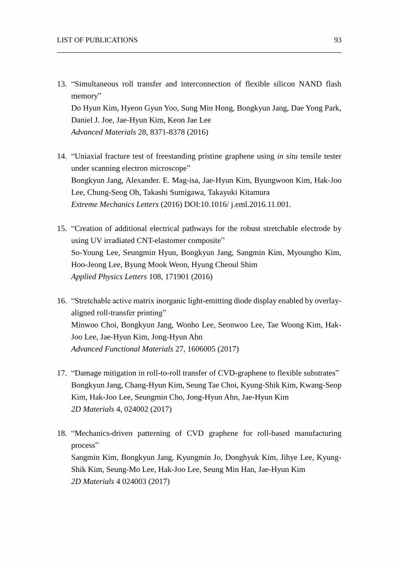
LIST OF PUBLICATIONS 93
13. “Simultaneous roll transfer and interconnection of flexible silicon NAND flash
memory”
Do Hyun Kim, Hyeon Gyun Yoo, Sung Min Hong, Bongkyun Jang, Dae Yong Park,
Daniel J. Joe, Jae-Hyun Kim, Keon Jae Lee
Advanced Materials 28, 8371-8378 (2016)
14. “Uniaxial fracture test of freestanding pristine graphene using in situ tensile tester
under scanning electron microscope”
Bongkyun Jang, Alexander. E. Mag-isa, Jae-Hyun Kim, Byungwoon Kim, Hak-Joo
Lee, Chung-Seog Oh, Takashi Sumigawa, Takayuki Kitamura
Extreme Mechanics Letters (2016) DOI:10.1016/ j.eml.2016.11.001.
15. “Creation of additional electrical pathways for the robust stretchable electrode by
using UV irradiated CNT-elastomer composite”
So-Young Lee, Seungmin Hyun, Bongkyun Jang, Sangmin Kim, Myoungho Kim,
Hoo-Jeong Lee, Byung Mook Weon, Hyung Cheoul Shim
Applied Physics Letters 108, 171901 (2016)
16. “Stretchable active matrix inorganic light-emitting diode display enabled by overlay-
aligned roll-transfer printing”
Minwoo Choi, Bongkyun Jang, Wonho Lee, Seonwoo Lee, Tae Woong Kim, Hak-
Joo Lee, Jae-Hyun Kim, Jong-Hyun Ahn
Advanced Functional Materials 27, 1606005 (2017)
17. “Damage mitigation in roll-to-roll transfer of CVD-graphene to flexible substrates”
Bongkyun Jang, Chang-Hyun Kim, Seung Tae Choi, Kyung-Shik Kim, Kwang-Seop
Kim, Hak-Joo Lee, Seungmin Cho, Jong-Hyun Ahn, Jae-Hyun Kim
2D Materials 4, 024002 (2017)
18. “Mechanics-driven patterning of CVD graphene for roll-based manufacturing
process”
Sangmin Kim, Bongkyun Jang, Kyungmin Jo, Donghyuk Kim, Jihye Lee, Kyung-
Shik Kim, Seung-Mo Lee, Hak-Joo Lee, Seung Min Han, Jae-Hyun Kim
2D Materials 4 024003 (2017)
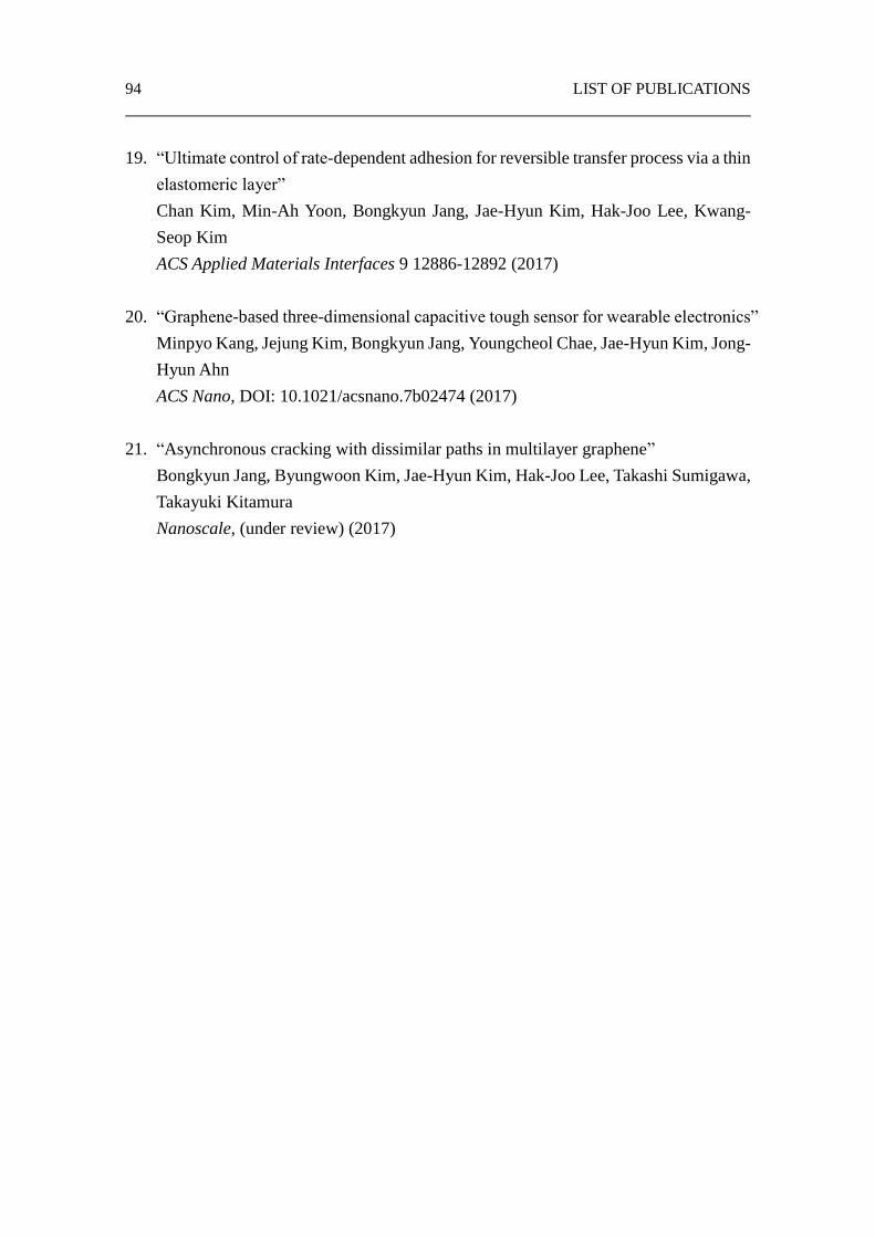
94 LIST OF PUBLICATIONS
19. “Ultimate control of rate-dependent adhesion for reversible transfer process via a thin
elastomeric layer”
Chan Kim, Min-Ah Yoon, Bongkyun Jang, Jae-Hyun Kim, Hak-Joo Lee, Kwang-
Seop Kim
ACS Applied Materials Interfaces 9 12886-12892 (2017)
20. “Graphene-based three-dimensional capacitive tough sensor for wearable electronics”
Minpyo Kang, Jejung Kim, Bongkyun Jang, Youngcheol Chae, Jae-Hyun Kim, Jong-
Hyun Ahn
ACS Nano, DOI: 10.1021/acsnano.7b02474 (2017)
21. “Asynchronous cracking with dissimilar paths in multilayer graphene”
Bongkyun Jang, Byungwoon Kim, Jae-Hyun Kim, Hak-Joo Lee, Takashi Sumigawa,
Takayuki Kitamura
Nanoscale, (under review) (2017)

ACKNOWLEDGEMENTS 95
Acknowledgements
Looking back my Ph.D. study in Kyoto and Daejeon, I would not complete it without
a great amount of supports and encouragements from my lovely family members,
excellent colleagues, and outstanding advisors.
First, I would like to express sincere appreciations and thanks to Professor Takayuki
Kitamura. It was a great fortune in my life that I met him at Kyoto University and he
became a supervisor in my Ph.D. research. Even though he was extremely busy with his
work as a dean of the department of engineering, he gladly assigned a time for a
discussion with me. His attitudes toward to research gave me tremendous inspirations and
ideas on fracture mechanics. His instructions make me acquire a wide vision to recognize
and understand academic area as well as the world. In addition, he has always made me
think about how to live my happy life. After starting my career as a researcher with a
Ph.D. degree, I wish he becomes a mentor in my future life as well.
I would like to sincerely thank Professor Shinji Nishiwaki and Professor Hiroyuki
Hirakata for their insightful advice, creative suggestions, and comments for future
research in my area. If I have a chance to research with them in future, I hope to receive
more academic instructions from them.
I wish to thank Associate Professor Takashi Sumigawa for a great number of his
supports in the experiments from the design of the experiments to the analysis of the
experimental results. His comments and guides assisted me to develop my research during
the study. In addition, I also appreciate his supports for me to live in Kyoto and to stay in
Material Science Lab. of Kyoto University.

96 ACKNOWLEDGEMENTS
I also appreciate Assistant Professor Takahiro Shimada for his inspiration for the
material designs and analytical viewpoint of mechanics with a constructive advice. His
insight into mechanics and multiphysics gave me a great impression in the research.
In addition, all of the members in Material Science Laboratory of Kyoto University
gave me great help to stay in Kyoto and Lab. in Katsura Campus. Dr. Le Van Lich, Dr.
Emi Kawai, Dr. Shaoguang Chen, Dr. Yanbin Yan, Byungwoon Kim, Xu Tao shared a
bunch of hurdles from the research to the writing this dissertation. I greatly thanks to their
understanding and help.
I would like to express great thanks to Dr. Hak-Joo Lee and Dr. Jae-Hyun Kim in
Korea Institute of Machinery and Materials (KIMM). I could not study in Kyoto
University without their great supports in South Korea. I also appreciate Dr. Byung-Ik
Choi and Dr. Sang-Rok Lee, which guided me a right way as a researcher. And I also
greatly thanks other members in Nanomechanics group of KIMM for a lot of help. In
addition, I appreciate the president and all members of KIMM.
Finally, I would like to express special thanks to my lovely wife, Seol and my son,
Jeyoon for their sacrifices during the study. And I wish to express great thanks to my
father and mother for constant supports and understandings for a long time.
Bongkyun Jang