Titanium nitride as a plasmonic material for visible and near
13
General rights Copyright and moral rights for the publications made accessible in the public portal are retained by the authors and/or other copyright owners and it is a condition of accessing publications that users recognise and abide by the legal requirements associated with these rights. Users may download and print one copy of any publication from the public portal for the purpose of private study or research. You may not further distribute the material or use it for any profit-making activity or commercial gain You may freely distribute the URL identifying the publication in the public portal If you believe that this document breaches copyright please contact us providing details, and we will remove access to the work immediately and investigate your claim. Downloaded from orbit.dtu.dk on: Oct 02, 2021 Titanium nitride as a plasmonic material for visible and near-infrared wavelengths Naik, Gururaj V.; Schroeder, Jeremy L.; Ni, Xingjie; Kildishev, Alexander V.; Sands, Timothy D.; Boltasseva, Alexandra Published in: Optical Materials Express Link to article, DOI: 10.1364/OME.2.000478 Publication date: 2012 Document Version Publisher's PDF, also known as Version of record Link back to DTU Orbit Citation (APA): Naik, G. V., Schroeder, J. L., Ni, X., Kildishev, A. V., Sands, T. D., & Boltasseva, A. (2012). Titanium nitride as a plasmonic material for visible and near-infrared wavelengths. Optical Materials Express, 2(4), 478-489. https://doi.org/10.1364/OME.2.000478
Transcript of Titanium nitride as a plasmonic material for visible and near

General rights Copyright and moral rights for the publications made accessible in the public portal are retained by the authors and/or other copyright owners and it is a condition of accessing publications that users recognise and abide by the legal requirements associated with these rights.
Users may download and print one copy of any publication from the public portal for the purpose of private study or research.
You may not further distribute the material or use it for any profit-making activity or commercial gain
You may freely distribute the URL identifying the publication in the public portal If you believe that this document breaches copyright please contact us providing details, and we will remove access to the work immediately and investigate your claim.
Downloaded from orbit.dtu.dk on: Oct 02, 2021
Titanium nitride as a plasmonic material for visible and near-infrared wavelengths
Naik, Gururaj V.; Schroeder, Jeremy L.; Ni, Xingjie; Kildishev, Alexander V.; Sands, Timothy D.;Boltasseva, Alexandra
Published in:Optical Materials Express
Link to article, DOI:10.1364/OME.2.000478
Publication date:2012
Document VersionPublisher's PDF, also known as Version of record
Link back to DTU Orbit
Citation (APA):Naik, G. V., Schroeder, J. L., Ni, X., Kildishev, A. V., Sands, T. D., & Boltasseva, A. (2012). Titanium nitride as aplasmonic material for visible and near-infrared wavelengths. Optical Materials Express, 2(4), 478-489.https://doi.org/10.1364/OME.2.000478

Titanium nitride as a plasmonic materialfor visible and near-infrared wavelengths
Gururaj V. Naik,1 Jeremy L. Schroeder,2 Xingjie Ni,1 Alexander V.Kildishev,1 Timothy D. Sands,1,2 and Alexandra Boltasseva1,3,∗1School of Electrical & Computer Engineering and Birck Nanotechnology Center,
Purdue University, West Lafayette, Indiana 47907, USA2School of Materials Engineering and Birck Nanotechnology Center, Purdue University,
West Lafayette, Indiana 47907, USA3DTU Fotonik, Technical University of Denmark, Lyngby 2800, Denmark
Abstract: The search for alternative plasmonic materials with improvedoptical properties, easier fabrication and integration capabilities over thoseof the traditional materials such as silver and gold could ultimately leadto real-life applications for plasmonics and metamaterials. In this work,we show that titanium nitride could perform as an alternative plasmonicmaterial in the visible and near-infrared regions. We demonstrate theexcitation of surface-plasmon-polaritons on titanium nitride thin films anddiscuss the performance of various plasmonic and metamaterial structureswith titanium nitride as the plasmonic component. We also show thattitanium nitride could provide performance that is comparable to that ofgold for plasmonic applications and can significantly outperform gold andsilver for transformation-optics and some metamaterial applications in thevisible and near-infrared regions.
© 2012 Optical Society of America
OCIS codes: (160.3918) Metamaterials; (250.5403) Plasmonics.
References and links1. W. Barnes, A. Dereux, and T. Ebbesen, “Surface plasmon subwavelength optics,” Nature 424, 824–830 (2003).2. S. Lal, S. Link, and N. Halas, “Nano-optics from sensing to waveguiding,” Nat. Photonics 1, 641–648 (2007).3. D. Smith, J. Pendry, and M. Wiltshire, “Metamaterials and negative refractive index,” Science 305, 788–792
(2004).4. W. Cai and V. Shalaev, Optical Metamaterials: Fundamentals and Applications (Springer Verlag, 2009).5. J. Pendry, D. Schurig, and D. Smith, “Controlling electromagnetic fields,” Science 312, 1780–1782 (2006).6. C. Soukoulis, S. Linden, and M. Wegener, “Physics: negative refractive index at optical wavelengths,” Science
315, 47–49 (2007).7. V. Shalaev, “Transforming light,” Science 322, 384–386 (2008).8. J. Pendry, “Negative refraction makes a perfect lens,” Phys. Rev. Lett. 85, 3966–3969 (2000).9. Z. Jacob, L. Alekseyev, and E. Narimanov, “Optical Hyperlens: Far-field imaging beyond the diffraction limit,”
Opt. Express 14, 8247–8256 (2006).10. S. Ramakrishna, J. Pendry, M. Wiltshire, and W. Stewart, “Imaging the near field,” J. Mod. Opt. 50, 1419–1430
(2003).11. W. Cai, U. Chettiar, A. Kildishev, and V. Shalaev, “Optical cloaking with metamaterials,” Nat. Photonics 1,
224–227 (2007).12. A. Kildishev and V. Shalaev, “Engineering space for light via transformation optics,” Opt. Lett. 33, 43–45 (2008).13. E. Narimanov and A. Kildishev, “Optical black hole: Broadband omnidirectional light absorber,” Appl. Phys.
Lett. 95, 041106 (2009).14. N. Fang, H. Lee, C. Sun, and X. Zhang, “Sub-diffraction-limited optical imaging with a silver superlens,” Science
308, 534–537 (2005).
#160717 - $15.00 USD Received 3 Jan 2012; revised 27 Feb 2012; accepted 28 Feb 2012; published 27 Mar 2012(C) 2012 OSA 1 April 2012 / Vol. 2, No. 4 / OPTICAL MATERIALS EXPRESS 478

15. Z. Liu, H. Lee, Y. Xiong, C. Sun, and X. Zhang, “Far-field optical hyperlens magnifying sub-diffraction-limitedobjects,” Science 315, 1686–1686 (2007).
16. V. Shalaev, W. Cai, U. Chettiar, H. Yuan, A. Sarychev, V. Drachev, and A. Kildishev, “Negative index of refractionin optical metamaterials,” Opt. Lett. 30, 3356–3358 (2005).
17. G. Dolling, M. Wegener, C. Soukoulis, and S. Linden, “Negative-index metamaterial at 780 nm wavelength,”Opt. Lett. 32, 53–55 (2007).
18. D. Schurig, J. Mock, B. Justice, S. Cummer, J. Pendry, A. Starr, and D. Smith, “Metamaterial electromagneticcloak at microwave frequencies,” Science 314, 977–980 (2006).
19. T. Ergin, N. Stenger, P. Brenner, J. Pendry, and M. Wegener, “Three-dimensional invisibility cloak at opticalwavelengths,” Science 328, 337–339 (2010).
20. A. Boltasseva and H. Atwater, “Low-loss plasmonic metamaterials,” Science 331, 290–291 (2011).21. P. Johnson and R. Christy, “Optical constants of the noble metals,” Phys. Rev. B 6, 4370–4379 (1972).22. G. Naik and A. Boltasseva, “Semiconductors for plasmonics and metamaterials,” Phys. Status Solidi (RRL) 4,
295–297 (2010).23. P. West, S. Ishii, G. Naik, N. Emani, V. Shalaev, and A. Boltasseva, “Searching for better plasmonic materials,”
Laser Photonics Rev. 4, 795–808 (2010).24. M. Noginov, L. Gu, J. Livenere, G. Zhu, A. Pradhan, R. Mundle, M. Bahoura, Y. Barnakov, and V. Podolskiy,
“Transparent conductive oxides: Plasmonic materials for telecom wavelengths,” Appl. Phys. Lett. 99, 021101(2011).
25. A. Frolich and M. Wegener, “Spectroscopic characterization of highly doped ZnO films grown by atomic-layerdeposition for three-dimensional infrared metamaterials,” Opt. Mater. Express 1, 883–889 (2011).
26. T. Minami, “New n-type transparent conducting oxides,” MRS Bull. 25, 38–44 (2000).27. G. Naik, J. Kim, and A. Boltasseva, “Oxides and nitrides as alternative plasmonic materials in the optical range,”
Opt. Mater. Express 1, 1090–1099 (2011).28. D. Park, T. Cha, K. Lim, H. Cho, T. Kim, S. Jang, Y. Suh, V. Misra, I. Yeo, J. Roh, J. Park, and H. Yoon, “Robust
ternary metal gate electrodes for dual gate CMOS devices,” in Electron Devices Meeting, 2001. IEDM TechnicalDigest. International (IEEE, 2001), pp. 30–36.
29. L. Hiltunen, M. Leskela, M. Makela, L. Niinisto, E. Nykanen, and P. Soininen, “Nitrides of titanium, niobium,tantalum and molybdenum grown as thin films by the atomic layer epitaxy method,” Thin Solid Films 166,149–154 (1988).
30. S. Aouadi and M. Debessai, “Optical properties of tantalum nitride films fabricated using reactive unbalancedmagnetron sputtering,” J. Vac. Sci. Technol. A 22, 1975–1979 (2004).
31. P. Patsalas and S. Logothetidis, “Optical, electronic, and transport properties of nanocrystalline titanium nitridethin films,” J. Appl. Phys. 90, 4725–4734 (2001).
32. B. Johansson, J. Sundgren, J. Greene, A. Rockett, and S. Barnett, “Growth and properties of single crystal TiNfilms deposited by reactive magnetron sputtering,” J. Vac. Sci. Technol. A 3, 303–307 (1985).
33. W.-C. Chen, Y.-R. Lin, X.-J. Guo, and S.-T. Wu, “Heteroepitaxial TiN of Very Low Mosaic Spread on Al2O3,”Jpn. J. Appl. Phys. 42, 208–212 (2003).
34. V. Drachev, U. Chettiar, A. Kildishev, H. Yuan, W. Cai, and V. Shalaev, “The Ag dielectric function in plasmonicmetamaterials,” Opt. Express 16, 1186–1195 (2008).
35. P. Berini, “Figures of merit for surface plasmon waveguides,” Opt. Express 14, 13030–13042 (2006).36. C. Davis, D. McKenzie, and R. McPhedran, “Optical properties and microstructure of thin silver films,” Opt.
Commun. 85, 70–82 (1991).37. Y. Yagil, P. Gadenne, C. Julien, and G. Deutscher, “Optical properties of thin semicontinuous gold films over a
wavelength range of 2.5 to 500 μm,” Phys. Rev. B 46, 2503–2511 (1992).38. K. Chen, V. Drachev, J. Borneman, A. Kildishev, and V. Shalaev, “Drude relaxation rate in grained gold nanoan-
tennas,” Nano Lett. 10, 916–922 (2010).39. X. Ni, Z. Liu, and A.V. Kildishev, “PhotonicsDB: Optical Constants,” http://nanohub.org/resources/PhotonicsDB.
(doi:10254/nanohub-r3692.10) (2010).40. J. A. Dionne, L. A. Sweatlock, H. A. Atwater, and A. Polman, “Plasmon slot waveguides: Towards chip-scale
propagation with subwavelength-scale localization,” Phys. Rev. B 73, 035407 (2006).41. S. Maier, Plasmonic Nanoguides and Circuits (Pan Stanford Publishing Pte. Ltd., 2009).42. M. Cortie, J. Giddings, and A. Dowd, “Optical properties and plasmon resonances of titanium nitride nanostruc-
tures,” Nanotechnol. 21, 115201 (2010).43. Z. Jacob, I. Smolyaninov, and E. Narimanov, “Broadband Purcell effect: Radiative decay engineering with meta-
materials,” Arxiv preprint arXiv:0910.3981 (2009).44. Z. Jacob, J.-Y. Kim, G. Naik, A. Boltasseva, E. Narimanov, and V. Shalaev, “Engineering photonic density of
states using metamaterials,” Appl. Phys. B 100, 215–218 (2010).45. G. Naik and A. Boltasseva, “A comparative study of semiconductor-based plasmonic metamaterials,” Metama-
terials 5, 1–7 (2011).46. G. Naik, J. Liu, A. Kildishev, V. Shalaev, and A. Boltasseva, “Negative refraction in Al:ZnO/ZnO metamaterial
in the near-infrared,” Arxiv preprint arXiv:1110.3231 (2011).
#160717 - $15.00 USD Received 3 Jan 2012; revised 27 Feb 2012; accepted 28 Feb 2012; published 27 Mar 2012(C) 2012 OSA 1 April 2012 / Vol. 2, No. 4 / OPTICAL MATERIALS EXPRESS 479
47. A. Hoffman, L. Alekseyev, S. Howard, K. Franz, D. Wasserman, V. Podolskiy, E. Narimanov, D. Sivco, andC. Gmachl, “Negative refraction in semiconductor metamaterials,” Nat. Mater. 6, 946–950 (2007).
48. V. Podolskiy and E. Narimanov, “Strongly anisotropic waveguide as a nonmagnetic left-handed system,” Phys.Rev. B 71, 201101 (2005).
49. J. Elser, V. Podolskiy, I. Salakhutdinov, and I. Avrutsky, “Nonlocal effects in effective-medium response ofnanolayered metamaterials,” Appl. Phys. Lett. 90, 191109 (2007).
50. S. Maier, Plasmonics: Fundamentals and Applications (Springer Verlag, 2007).51. A. Hibbins, J. Sambles, and C. Lawrence, “Surface plasmon-polariton study of the optical dielectric function of
titanium nitride,” J. Mod. Opt. 45, 2051–2062 (1998).52. X. Ni, Z. Liu, A. Boltasseva, and A. Kildishev, “The validation of the parallel three-dimensional solver for
analysis of optical plasmonic bi-periodic multilayer nanostructures,” Appl. Phys. A 100, 365–374 (2010).
1. Introduction
Plasmonics [1,2] and metamaterials (MMs) [3,4] have advanced enormously in the past decadebringing about a paradigm shift from conventional photonics. Together with transformationoptics (TO) [5–7], plasmonics and MMs have produced a new set of ideas such as negative re-fractive index materials [8], nanoscale imaging devices [9,10], invisibility cloaks [11] and lightconcentrators [12, 13], thus paving the way for the realization of devices with unprecedentedfunctionalities [14–19]. Although the experimental realizations of these devices serve as excit-ing demonstrations of the phenomena, practical applications thus far are limited. One of themajor challenges hindering MM and TO applications in real devices is the large loss comingfrom the plasmonic components of these devices [20]. Conventional plasmonic materials suchas gold and silver exhibit excessive losses at optical frequencies [21], making them less suitablefor real-world devices. In addition to the problem of loss, another major issue associated withthe use of conventional metals in device applications is that the real parts of metal permittivitiesare too large in magnitude to be useful for many TO and MM devices [12]; ideally, the per-mittivity of the plasmonic material in a device would be adjustable. Another important factoris the ease of integration of the plasmonic material with standard semiconductor fabricationprocesses. The easy integration of plasmonic devices could allow the leveraging of standardsemiconductor manufacturing technologies and processes for combining plasmonic materialswith semiconductor devices.
In the search for better plasmonic materials, transparent conducting oxides (TCOs) wereproposed as good alternatives to gold and silver in the near-infrared (near-IR) range [22–25].However, TCOs cannot be plasmonic (i.e. exhibiting metallic properties) at visible wavelengthsbecause the carrier concentration is limited to around 1021 cm−3 [26]. Transition-metal nitridessuch as titanium nitride and zirconium nitride can have carrier concentrations higher than thoseachievable in TCOs [27]. Despite the fact that the optical losses are not smaller than thoseof noble metals, the magnitude of the real permittivity of these metal nitrides in the visiblerange is much smaller than that of noble metals owing to the smaller carrier concentration.Additionally, the optical properties of these metal nitrides may be tuned, unlike the case fornoble metals, simply by changing the processing conditions [27]. Another major advantage oftitanium nitride and zirconium nitride is that they offer easy fabrication and integration withstandard silicon manufacturing processes [28]. All of the above factors make transition metalnitrides promising alternative plasmonic materials in the visible and near-IR regions.
This paper focuses on titanium nitride for plasmonic and metamaterial applications in thevisible and near-IR regions. We present the optimization of processing conditions as well asmaterial and optical characterization results for TiN thin films. We also provide a comparativestudy of the performance of various plasmonic and metamaterial devices with TiN as the plas-monic material. The paper concludes with the demonstration of the plasmonic properties of TiNthin films by exciting surface plasmon polaritons (SPPs) on these films.
#160717 - $15.00 USD Received 3 Jan 2012; revised 27 Feb 2012; accepted 28 Feb 2012; published 27 Mar 2012(C) 2012 OSA 1 April 2012 / Vol. 2, No. 4 / OPTICAL MATERIALS EXPRESS 480

2. Titanium nitride: deposition and characterization
Transition metal nitrides such as TiN are ceramic materials that are non-stoichiometric. In otherwords, the composition and hence the optical properties depend significantly on the prepa-ration method and conditions. Some of these nitrides possess metallic properties at visiblewavelengths because of large free carrier concentrations (≈ 1022cm−3) [29–31]. High inter-band losses make many of these compounds unattractive for plasmonic applications. Titaniumnitride, however, exhibits smaller interband losses in the red part of the visible spectrum anda small negative real permittivity [31]. It is therefore a material of significant interest for plas-monic applications in the visible and near-IR ranges.
Thin films of titanium nitride were deposited on glass or c-sapphire substrates by DC reactivemagnetron sputtering (PVD Products Inc.) from a 99.995% titanium target in an argon-nitrogenenvironment. The base pressure within the chamber before deposition was 2× 10⁻⁷ Torr. Thefilms were deposited at a pressure of 5 mTorr with varying flow ratios of argon and nitrogen(Ar (sccm):N2 (sccm) of 4:6, 2:8 and 0:10). The sputtering power was held constant for alldepositions at 200 W (DC) and the target-substrate distance was 8 cm. The deposition rate wasapproximately 25 A/min and about 30 nm thick films were deposited. The substrate tempera-ture during deposition was held at 300 oC or 500 oC. The resulting films were characterized bya variable angle spectroscopic ellipsometer (V-VASE, J.A. Woollam Co.) in the near-IR, visi-ble and near-UV wavelength ranges. A Drude-Lorentz (with three Lorentz oscillators) modelprovided a good fit to the ellipsometric measurements. The Drude part of the model capturesthe part of the optical response arising from free carriers, while the Lorentz oscillators accountfor the interband losses. Figure 1 shows the dielectric functions retrieved for three TiN filmsdeposited at 300 oC on c-sapphire substrates with different flow ratios of argon and nitrogen.Note that the Drude damping of the carriers does not vary significantly among the three films.However, the unscreened plasma frequency increases slightly for the film deposited at a flowratio of 2:8 (Ar:N2), which results in higher loss compared to the other films.
The influence of the substrate temperature on the optical properties of these films was studiedby depositing TiN films at substrate temperatures of 300 oC and 500 oC with the Ar:N2 flowratio fixed at 4:6. Figure 2 shows the dielectric function extracted for these two films. Clearly,the film deposited at the higher temperature shows lower loss.
The optical properties of TiN thin films also depend strongly on the substrate on whichthey are grown. Substrates such as sapphire and MgO provide lattice matching and promoteepitaxial growth [32, 33], leading to crystalline films and thereby reducing optical losses [34].Substrates such as glass do not provide lattice matching and polycrystalline films are obtainedwhich can have higher losses due to additional carrier scattering. The optical properties of aTiN film grown on c-sapphire and glass are shown in Fig. 3. The film grown on glass showslower carrier concentration and higher losses than the film grown on c-sapphire. In order toverify if c-sapphire allows epitaxial growth of TiN films, X-ray diffraction (Phillips X’PertPro) measurements were performed. The diffraction intensity plot for TiN thin films on c-sapphire substrate is shown in Fig. 4. The 2θ −ω plot shows two peaks corresponding to the111 reflection from TiN and the 0006 reflection from sapphire substrate. TiN film on c-sapphiregrows essentially in the [111] direction. Further, the epitaxial growth of TiN on c-sapphire isconfirmed by performing an asymmetric-phi scan. In this measurement, the x-ray detector (2θ )and the incidence angle at the sample (ω) are fixed at values corresponding to the 200 reflection.The off-plane tilt of the sample (χ) is set to 54.7 degrees corresponding to the interplanar anglebetween (200) and (111) planes. Epitaxial growth would be evidenced by peaks correspondingto three 200 reflections when the sample is rotated by 360 degrees. The inset in Fig. 4 showsthe result of an asymmetric-phi scan on a TiN film deposited on a c-sapphire substrate. Thesix sharp peaks observed in this measurement confirm mutivariant epitaxial growth of TiN on
#160717 - $15.00 USD Received 3 Jan 2012; revised 27 Feb 2012; accepted 28 Feb 2012; published 27 Mar 2012(C) 2012 OSA 1 April 2012 / Vol. 2, No. 4 / OPTICAL MATERIALS EXPRESS 481

0 500 1000 1500 2000−30
−25
−20
−15
−10
−5
0
5
Wavelength (nm)
ε'
Ar:N2=4:6Ar:N2=2:8Ar:N2=0:10
0 500 1000 1500 20000
5
10
15
20
25
30
35
Wavelength (nm)
ε"
Ar:N2=4:6Ar:N2=2:8Ar:N2=0:10
Fig. 1. Dielectric functions of sputter-deposited titanium nitride films retrieved by spectro-scopic ellipsometry measurements. The films were deposited on c-sapphire substrates byDC reactive magnetron sputtering at 300 oC with different flow ratios (sccm:sccm) of argonand nitrogen.
c-sapphire.Epitaxial growth of TiN thin films on c-sapphire produces films that have low roughness and
are uniformly textured. In Fig. 5, we show representative atomic force microscope (AFM) andscanning electron micrograph (SEM) images of a TiN film on a c-sapphire substrate. The root-mean-square (rms) roughness of the film is measured to be about 0.4 nm as shown in Fig 5a.Although the film is smoother than a polycrystalline film, the boundaries between domains ofepitaxial variants of cubic TiN introduce a degree of roughness.
3. Plasmonic and metamaterial applications
In this section, we consider TiN as a plasmonic building block for different applications suchas SPP waveguides, localized surface plasmon resonance (LSPR) devices, hyperbolic MMs,and general transformation optics devices. The figures-of-merit of these devices with TiN asplasmonic component are evaluated and compared against their elemental metal based counter-parts.
3.1. Plasmonic applications
An SPP propagating along a single metal/air interface is characterized by two important pa-rameters: the propagation length (defined as the 1/e field-decay length along the direction ofpropagation) and the confinement width (the 1/e field-decay width on each side of the inter-face) [35]. There is a trade-off between these parameters such that weaker confinement resultsin a longer propagation length and vice versa. In general, the trade-off is very sensitive tolosses in the metal and decreases sharply with higher damping losses. Since it has the lowestDrude damping, silver offers the best SPP characteristics. However, problems in fabricatingthin films of silver and its chemical reactivity in air preclude it from being useful for some ap-plications [34, 36]. Gold is better due its chemical stability, but it poses other problems arisingfrom nanofabrication such as poor adhesion to substrates and the formation of percolating or
#160717 - $15.00 USD Received 3 Jan 2012; revised 27 Feb 2012; accepted 28 Feb 2012; published 27 Mar 2012(C) 2012 OSA 1 April 2012 / Vol. 2, No. 4 / OPTICAL MATERIALS EXPRESS 482

500 1000 1500 2000−30
−25
−20
−15
−10
−5
0
5
Wavelength (nm)
ε'
300 oC500 oC
500 1000 1500 20000
3
6
9
12
15
18
21
ε"
Fig. 2. Dielectric functions of titanium nitride films deposited at 300 oC and 500 oC re-trieved by spectroscopic ellipsometry measurements. The films were deposited with theflow ratio of argon and nitrogen set to 4:6.
500 1000 1500 2000−35
−30
−25
−20
−15
−10
−5
0
5
Wavelength (nm)
ε'
on glasson c−sapphire
500 1000 15000
10
20
30
40
50
60
70
80
ε"
Fig. 3. Dielectric functions of titanium nitride films deposited at 300 oC on glass and c-sapphire substrates.
semicontinuous films when the thickness is around 10 nm or lower [37, 38]. Such problemsarising from the growth and morphology of gold films result in additional optical losses, whichcan be described by a phenomenological quantity called the loss factor [34,38]. This loss factordirectly multiplies the Drude-damping rate and increases the imaginary part of the permittivityfor values greater than unity. In the following comparative study, the optical properties of noblemetals are derived from the well-known work by Johnson and Christy (JC) [21,39] and the lossfactor is applied onto this data.
Figure 6 shows the propagation lengths and confinements for SPPs along the interface be-tween air and TiN, air and gold, and air and gold with a loss factor of 3.5. Note that TiN gives aslightly better confinement than gold, but the propagation length for TiN is smaller than that for
#160717 - $15.00 USD Received 3 Jan 2012; revised 27 Feb 2012; accepted 28 Feb 2012; published 27 Mar 2012(C) 2012 OSA 1 April 2012 / Vol. 2, No. 4 / OPTICAL MATERIALS EXPRESS 483

30 40 50 60 70
101
102
103
104
105
2θ (deg)
Inte
nsity
(a.u
)
0 100 200 300102
103
φ (deg)
Inte
nsity
(a.u
)
TiN
111
Sap
phire
00
06Fig. 4. X-ray diffraction plot showing the diffraction intensity from a TiN thin film grownon c-sapphire. The peaks in the intensity correspond to the crystal planes annotated. Theinset shows the intensity plot for an asymmetric-phi scan with 2θ set to the 200 reflectionof TiN and off-plane tilt angle (χ) set to 54.7 degrees corresponding to interplanar anglebetween (111) and (200) planes.
100 nm100 nm
a)a)
b)b)
250500
750250
500
750
04 nm
0
-2 nm
2 nm
1000 nm
1000 nm
Fig. 5. Characterization of 30 nm thick TiN film deposited on a c-sapphire substrate. a)Atomic force microscope (AFM) image b) Scanning electron micrograph.
gold. The characteristics of TiN resemble that of gold with a loss factor of 3.5. As a comparisonpoint, a loss factor of 3.5 or higher is commonly observed in nanopatterned gold structures.
Instead of the simple case of SPPs propagating along a single interface, more complicateddesigns such as a metal-insulator-metal (MIM) waveguide geometry with TiN are also worthconsidering [40]. The MIM configuration allows confinement of a significant portion of theelectromagnetic field within the insulator and, hence, the propagation length of SPPs in thisconfiguration is a fair index for comparing the performance of different plasmonic material
#160717 - $15.00 USD Received 3 Jan 2012; revised 27 Feb 2012; accepted 28 Feb 2012; published 27 Mar 2012(C) 2012 OSA 1 April 2012 / Vol. 2, No. 4 / OPTICAL MATERIALS EXPRESS 484
600 800 1000 1200 1400 1600 1800 2000
100
101
102
Wavelength (nm)
Prop
agat
ion
leng
th (μ
m)
TiNGoldGold (loss factor=3.5)
a)
600 800 1000 1200 1400 1600 1800 2000
100
101
Wavelength (nm)
Mod
e si
ze (μ
m)
TiNGoldGold (loss factor=3.5)
b)
Fig. 6. Comparison of the performance characteristics of SPP waveguides formed by theinterface of air with TiN-, gold (JC)- and gold with loss factor of 3.5: a) Propagation length(1/e field decay length along the propagation direction) b) Confinement width (1/e fielddecay widths on each side normal to the interface).
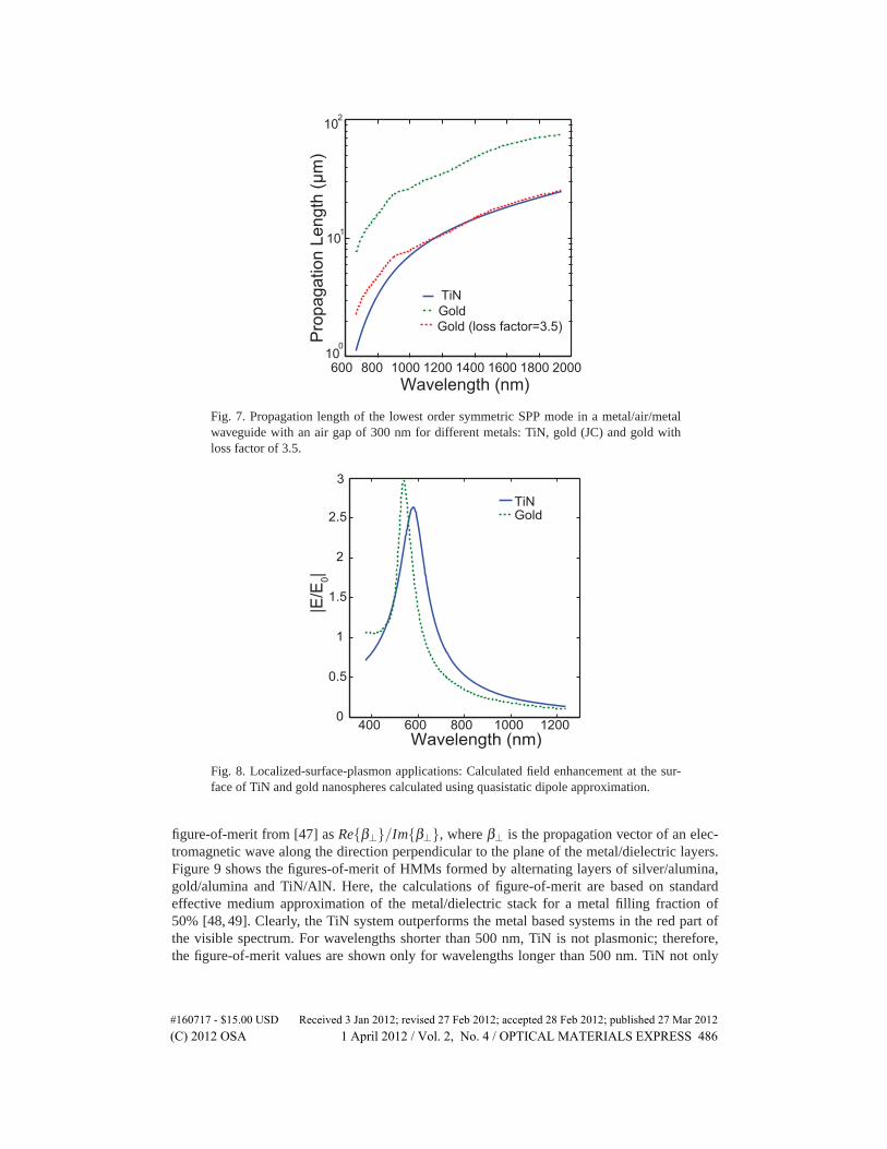
systems. Figure 7 shows the propagation lengths calculated [41] for the lowest order symmetricSPP mode in an MIM waveguide with a 300 nm air gap as the insulator and TiN or gold as themetal. The propagation length is smaller for the case of TiN compared to gold with a unity lossfactor. However, the propagation length of a TiN waveguide is comparable to that of gold witha loss factor of 3.5.
In addition to propagating modes, localized surface plasmon resonance (LSPR) modes areuseful in many sensing applications where localized field enhancement is of great importance[2]. Metal nanoparticles can support LSPR modes and enable local-field enhancement. Thefield enhancements at the surface of TiN and gold nanospheres calculated using the quasistaticdipole approximation are shown in Fig. 8. The resonance wavelength (which corresponds tothe peak field enhancement) for TiN nanospheres is red-shifted compared to gold owing toTiN’s smaller absolute real permittivity value [42]. The magnitude of field enhancement in TiNnanospheres is slightly smaller than that of gold, but the overall performance of each materialis comparable, making TiN a realistic alternative plasmonic material for LSPR applications.
3.2. Hyperbolic metamaterials and transformation optics
MMs with hyperbolic dispersion are receiving increasing attention from researchers because oftheir unique properties such as the propagation of extremely high-k waves [9] and a broadbandsingularity in the photonic-density-of-states (PDOS) [43]. These properties have resulted in de-vices such as the hyperlens [9] and phenomena such as engineering the spontaneous emissionrate [44], both of which have useful applications in quantum optics. Hyperbolic MMs (HMMs)can be easily fabricated by stacking alternating, sub-wavelength layers of metal and dielectricmaterials. For example, the first demonstration of a hyperlens used alternating layers of silverand alumina [15]. However, such a material system works well only in the near-UV where theperformance of silver is best-suited for HMMs. In the visible spectrum, neither gold nor sil-ver can produce high-performance HMMs [45,46]. To compare the performance, we adopt the
#160717 - $15.00 USD Received 3 Jan 2012; revised 27 Feb 2012; accepted 28 Feb 2012; published 27 Mar 2012(C) 2012 OSA 1 April 2012 / Vol. 2, No. 4 / OPTICAL MATERIALS EXPRESS 485
600 800 1000 1200 1400 1600 1800 200010
0
101
102
Wavelength (nm)
Pro
paga
tion
Leng
th (μ
m)
TiNGoldGold (loss factor=3.5)
Fig. 7. Propagation length of the lowest order symmetric SPP mode in a metal/air/metalwaveguide with an air gap of 300 nm for different metals: TiN, gold (JC) and gold withloss factor of 3.5.
400 600 800 1000 12000
0.5
1
1.5
2
2.5
3
Wavelength (nm)
|E/E
0|
TiNGold
Fig. 8. Localized-surface-plasmon applications: Calculated field enhancement at the sur-face of TiN and gold nanospheres calculated using quasistatic dipole approximation.
figure-of-merit from [47] as Re{β⊥}/Im{β⊥}, where β⊥ is the propagation vector of an elec-tromagnetic wave along the direction perpendicular to the plane of the metal/dielectric layers.Figure 9 shows the figures-of-merit of HMMs formed by alternating layers of silver/alumina,gold/alumina and TiN/AlN. Here, the calculations of figure-of-merit are based on standardeffective medium approximation of the metal/dielectric stack for a metal filling fraction of50% [48, 49]. Clearly, the TiN system outperforms the metal based systems in the red part ofthe visible spectrum. For wavelengths shorter than 500 nm, TiN is not plasmonic; therefore,the figure-of-merit values are shown only for wavelengths longer than 500 nm. TiN not only
#160717 - $15.00 USD Received 3 Jan 2012; revised 27 Feb 2012; accepted 28 Feb 2012; published 27 Mar 2012(C) 2012 OSA 1 April 2012 / Vol. 2, No. 4 / OPTICAL MATERIALS EXPRESS 486

500 1000 1500 200010
−3
10−2
10−1
100
101
102
Wavelength (nm)
FoM
= β
' ┴ /
β'' ┴
TiN / AlNGold / AluminaSilver / Alumina
Fig. 9. Figures-of-merit for HMMs formed by alternating, sub-wavelength layers of differ-ent metal/dielectric combinations (TiN/AlN, silver/alumina and gold/alumina).
outperforms in its performance, but also provides an additional advantage in the fabrication ofultra-thin layers. Ultra-thin layers are necessary for producing truly binary HMM structure andTiN, unlike metals can be grown as an ultra-thin epitaxial layer.
In general, transformation optics devices often require plasmonic components with real per-mittivity values that are on the order of unity. While none of the conventional metals satisfythis condition, titanium nitride does meet this criterion and is therefore a suitable material thatcould enable transformation optics in the visible range. As a comparison, the dielectric func-tions of TiN and bulk, conventional metals are plotted in Fig. 10. The figure clearly showsthe disadvantage of conventional metals in terms of the real part of permittivity. However, theimaginary part of permittivity, which signifies the losses in the material, is the lowest in thecase of silver. TiN is better than gold only for longer wavelengths. In practical applications, it israther difficult to obtain low, bulk-like losses in designs using silver because of problems suchas surface roughness, grain-boundary scattering and corrosion. Also, forming ultra-thin layersof silver or gold is difficult. On the contrary, TiN does not possess such difficulties and forms abetter materials choice than conventional metals for TO applications.
4. Excitation of SPPs
In order to demonstrate the plasmonic behavior of TiN, we studied the properties of SPPsat the interface of TiN and a dielectric. Since SPPs have momentum that is larger than thatsupported in the dielectric, direct excitation of SPP modes is not possible. However, manydifferent techniques can be employed to excite SPPs on an interface [50]. In this work wedemonstrate the excitation of SPPs on 30-nm-thick films of TiN using the grating couplingtechnique [51]. Initially, about 110 nm of an electron-beam resist (ZEP) is spin-coated on theTiN film and patterned into dielectric gratings with a periodicity of 1.5 μm (see inset of Fig.11). The angular reflectance of this structure was measured using a variable-angle spectroscopicellipsometer (J.A. Woollam Co.). The incident beam was TM polarized, and the gratings werealigned parallel to the incident magnetic field. The angular reflectance measured at two differentwavelengths in the near-IR range is shown Fig. 11. The dips in reflectance observed around 30and 25 degrees for wavelengths of 900 and 1000 nm respectively correspond to the excitation of
#160717 - $15.00 USD Received 3 Jan 2012; revised 27 Feb 2012; accepted 28 Feb 2012; published 27 Mar 2012(C) 2012 OSA 1 April 2012 / Vol. 2, No. 4 / OPTICAL MATERIALS EXPRESS 487

500 1000 1500 2000−100
−80
−60
−40
−20
0
Wavelength (nm)
ε'
TiNAgAu
500 1000 1500 20000
5
10
15
20
25
30
Wavelength (nm)
ε"
TiNAgAu
Fig. 10. Dielectric function of TiN in comparison with conventional plasmonic materials:gold and silver (data adapted from JC [21,39]).
SPPs along the interface. We confirmed that this observed behavior arises due to SPP excitationby computing the SPP dispersion curve for a TiN/ZEP interface and the momentum mismatchbetween the SPP-curve and the light line of the dielectric. The additional momentum requiredto couple SPPs is provided exactly by the grating at these angles of incidence, producing a dipin the observed reflectance. The reflectance dip is shallow owing to the weak coupling offeredby the thin dielectric grating. A thicker dielectric grating or a plasmonic grating formed bypatterning the TiN film could overcome this problem and provide stronger SPP coupling.
The observed optical phenomenon was also verified through simulations using the spatialharmonic analysis (SHA) method [52]. The optical constants of the TiN film and dielectricpolymer (ZEP) for the simulations were obtained from ellipsometry measurements as statedabove. The thickness of the dielectric gratings was adjusted from the measured value within5% to match the experimental curves. The results of the calculations are shown in Fig. 11 fortwo different excitation wavelengths. The calculations match the experiments reasonably well,confirming the excitation of SPPs on the TiN film.
5. Conclusion
We have shown that titanium nitride can serve as an alternative plasmonic material for plas-monic and metamaterial applications in the visible and near-IR frequencies. We showed thattitanium nitride, being a non-stoichiometric compound, exhibits process-dependent properties.Thin TiN films deposited on c-sapphire substrates showed multivariant epitaxial growth andformed smooth films. Our comparative study of TiN and conventional plasmonic materialssuggested that TiN offers comparable performance for plasmonic applications and significantlybetter performance for transformation optics and metamaterial devices such as hyperbolic meta-material devices. Titanium nitride was shown to support SPPs in the near-IR range by usingdielectric gratings to excite SPPs on TiN/dielectric interfaces. An inherent advantage of TiNis that it is compatible with standard silicon manufacturing processes, unlike gold and silver.This could allow easy integration of silicon electronics with plasmonics. Titanium nitride alsoovercomes many other nanofabrication problems associated with gold and silver, making it a
#160717 - $15.00 USD Received 3 Jan 2012; revised 27 Feb 2012; accepted 28 Feb 2012; published 27 Mar 2012(C) 2012 OSA 1 April 2012 / Vol. 2, No. 4 / OPTICAL MATERIALS EXPRESS 488

λ = 900 nmλ = 1000 nm
20 30 40 50 60 70 800.35
0.4
0.45
0.5
0.55
0.6
0.65
0.7
0.75
Ref
lect
ance
Angle of incidence (deg)
Sapphire
TiN(25 nm)
Dielectric gratings
Fig. 11. Angular reflectance of dielectric (ZEP, electron-beam resist) gratings formed on topof a 30 nm thick film of TiN. The inset shows the geometry of the structure. The measured(solid lines) and calculated (dashed lines) reflectances are plotted against angle of incidencefor two different wavelengths.
technologically important alternative plasmonic material.
Acknowledgments
We thank Prof. Vladimir M. Shalaev for useful discussions. This work was supported in partby ARO grant number W911NF-11-1-0359 and ONR-MURI grant N00014-10-1-0942. Dr.A.V. Kildishev was partially supported by the AFRL Materials and Manufacturing DirectorateApplied Metamaterials Program.
#160717 - $15.00 USD Received 3 Jan 2012; revised 27 Feb 2012; accepted 28 Feb 2012; published 27 Mar 2012(C) 2012 OSA 1 April 2012 / Vol. 2, No. 4 / OPTICAL MATERIALS EXPRESS 489