
TinySwitch II PIDesign1
7
-
Upload
elias-moreira-campos -
Category
Documents
-
view
71 -
download
4
Transcript of TinySwitch II PIDesign1
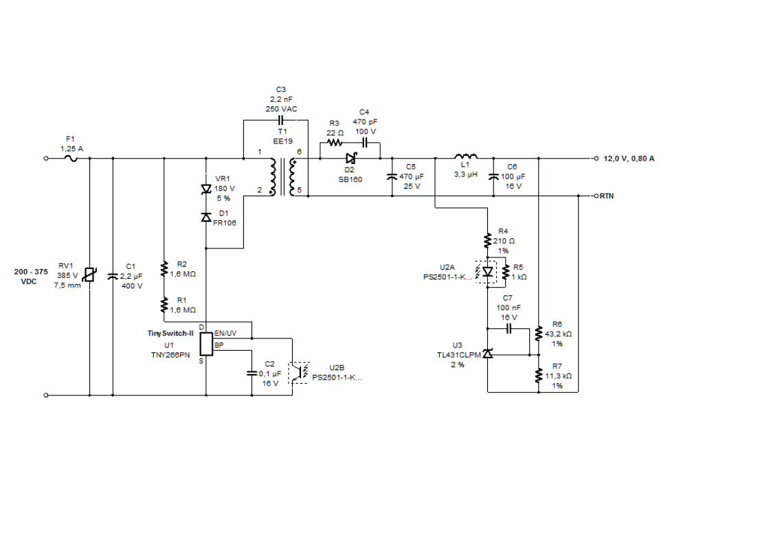

Power Supply InputVar Value Units DescriptionVDCMIN 200 V Minimum Input DC VoltageVDCMAX 375 V Maximum Input DC VoltageZ 0,70 Loss Allocation Factorŋ 78,0 % Efficiency EstimateIAVG 0,07 A Average Diode Bridge Current (DC Input Current)
Input SectionVar Value Units DescriptionFuse 1,25 A Input Fuse Rated CurrentMOV_VRATED 385 V MOV Rated Voltage
Device VariablesVar Value Units DescriptionDevice TNY266PN PI Device NameDevice Mode Default Current Limit mode for devicePO 10,40 W Total Output PowerVDRAIN Estimated 592,50 V Actual Estimated Drain VoltageVDS 11,00 V On state Drain to Source VoltageFSMIN 120000 Hz Minimum Switching FrequencyKP 0,97 Continuous/Discontinuous Operating RatioILIMITMIN 0,33 A Minimum Current LimitILIMITMAX 0,38 A Maximum Current LimitRLS 1,6 MΩ Line sense resistorRLS2 1,6 MΩ Line sense resistorIRMS 0,13 A Primary RMS Current (at VMIN)P_NO_LOAD 300 mW Estimated No Load Input PowerDMAX 0,42 Maximum Duty CycleRTH_DEVICE 119,63 °C/W PI Device Maximum Thermal Resistance
2 Oz (70 µ)Copper PCB
PI Device Heatsink Type
52 mm² PI Device Heatsink Area
Clamp CircuitVar Value Units DescriptionClamp Type Zener Clamp Clamp Circuit TypeVCLAMP 180 V Estimated average clamping voltageEstimated ClampLoss
0,43 W Clamp Dissipation
Transformer Construction ParametersVar Value Units DescriptionCore Type EE19 Core TypeCore Material NC-2H (Nicera)
or EquivalentCore Material
Bobbin Reference Generic, 4 pri. +5 sec.
Bobbin Reference
Bobbin Orientation Vertical Bobbin typePrimary Pins 4 Number of Primary pins usedSecondary Pins 2 Number of Secondary pins usedUSE_SHIELDS NO Use shield WindingsLP_nom 2185 µH Nominal Primary InductanceLP_Tol 10,0 % Primary Inductance ToleranceNP 116,9 Calculated Primary Winding Total Number of TurnsNSM 11 Secondary Main Number of TurnsCMA 394 Cmils/A Primary Winding Current CapacityVOR 135,0 V Reflected Output VoltageBW 9,00 mm Bobbin Winding WidthML 0,00 mm Safety Margin on Left WidthMR 0,00 mm Safety Margin on Right WidthFF 46 % Actual Transformer Fit Factor. 100% signifies fully utilized winding windowAE 23,00 mm² Core Cross Sectional AreaALG 144 nH/T² Gapped Core Effective InductanceBM 2891 Gauss Maximum Flux Density

BAC 1206 Gauss AC Flux Density for Core LossLG 0,178 mm Estimated Gap LengthL_LKG 65,56 µH Estimated primary leakage inductanceLSEC 15 nH Secondary Trace Inductance
Primary Winding Section 1Var Value Units DescriptionNP1 117 Rounded (Integer) Number of Primary winding turns in the first section of primaryWire Size 33 AWG Wire size of primary windingWinding Type Single (x1) Primary winding number of parallel wire strandsL 2,81 Primary Number of LayersDC Copper Loss 0,04 W Primary 1 DC Losses
Output 1Var Value Units DescriptionVO 12,00 V Output VoltageIO 0,80 A Output CurrentVOUT_ACTUAL 12,00 V Actual Output VoltageNS 11 Secondary Number of TurnsWire Size 25 AWG Wire size of secondary windingWinding Type Single (x1) Output winding number of parallel strandsL_S_OUT 0,79 Secondary Output Winding LayersDC Copper Loss 0,11 W Secondary DC LossesVD 0,70 V Output Winding Diode Forward Voltage DropPIVS 47 V Output Rectifier Maximum Peak Inverse VoltageISP 3,19 A Peak Secondary CurrentISRMS 1,43 A Secondary RMS CurrentRTH_DIODE 89,83 °C/W Output Diode Maximum Thermal ResistanceOD_HSINK_TYPE 2 Oz (70 µ)
Copper PCBOutput Diode Heatsink Type
OD_HSINK_AREA 52 mm² Output Diode Heatsink AreaCO 470 x 1 µF Output CapacitorIRIPPLE 1,18 A Output Capacitor RMS Ripple CurrentExpected Lifetime 25791 hr Expected Lifetime of Output Capacitor
Feedback CircuitVar Value Units Description
NO Dual Output Feedback regulations use flagSF_FLAG NO Soft Finish Circuits use flag
NO Phase Boost Network flag
The regulation and tolerances do not account for thermal drifting and component tolerance of the output diode forward voltage drop and voltage drops across the LC post filter. The actualvoltage values are estimated at full load only.Please verify cross regulation performance on the bench.

Board Layout Recommendations
Click on the "Show me" icon to highlight relevant areas on the sample layout.
Description Show Me1 Maximize source area for good heat-sinking2 Keep drain trace short3 The BYPASS pin capacitor should be located as close as possible to the BYPASS and SOURCE pins4 Keep noisy traces away from EN/UV pin5 Route bias winding currents back to the bulk cap6 Keep clamp loop short7 Connect Y capacitor to the B+ rail on the primary side for better surge immunity. Keep Y capacitor traces short8 The area of the loop connecting the secondary winding, the output diode and the output filter capacitor should be minimized
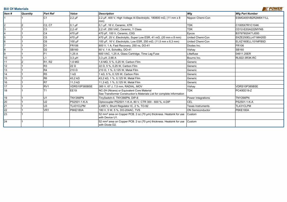
Bill Of MaterialsItem # Quantity Part Ref Value Description Mfg Mfg Part Number1 1 C1 2,2 µF 2,2 µF, 400 V, High Voltage Al Electrolytic, 180800 mΩ, (11 mm x 8
mm)Nippon Chemi-Con ESMG400VB2R2M8X11LL
2 2 C2, C7 0,1 µF 0,1 µF, 16 V, Ceramic, X7R TDK C1005X7R1C104K3 1 C3 2,2 nF 2,2 nF, 250 VAC, Ceramic, Y Class TDK CD12-E2GA222MYNS4 1 C4 470 pF 470 pF, 100 V, Ceramic, C0G Epcos B37979G5471J0005 1 C5 470 µF 470 µF, 25 V, Electrolytic, Super Low ESR, 41 mΩ, (20 mm x 8 mm) United Chemi-Con EKZE250ELL471MH20D6 1 C6 100 µF 100 µF, 16 V, Electrolytic, Low ESR, 250 mΩ, (11,5 mm x 6,3 mm) United Chemi-Con ELXZ160ELL101MFB5D7 1 D1 FR106 800 V, 1 A, Fast Recovery, 250 ns, DO-41 Diodes Inc. FR1068 1 D2 SB160 60 V, 1 A, Schottky, DO-41 Vishay SB1609 1 F1 1,25 A 600 VAC, 1,25 A, Glass Cartridge, Time Lag Fuse Littelfuse 04611.25ER10 1 L1 3,3 µH 3,3 µH, 2,66 A Bourns Inc. RL822-3R3K-RC11 2 R1, R2 1,6 MΩ 1,6 MΩ, 5 %, 0,25 W, Carbon Film Generic12 1 R3 22 Ω 22 Ω, 5 %, 0,25 W, Carbon Film Generic13 1 R4 210 Ω 210 Ω, 1 %, 0,125 W, Metal Film Generic14 1 R5 1 kΩ 1 kΩ, 5 %, 0,125 W, Carbon Film Generic15 1 R6 43,2 kΩ 43,2 kΩ, 1 %, 0,125 W, Metal Film Generic16 1 R7 11,3 kΩ 11,3 kΩ, 1 %, 0,125 W, Metal Film Generic17 1 RV1 VDRS10P385BSE 385 V, 67 J, 7,5 mm, RADIAL, MOV Vishay VDRS10P385BSE18 1 T1 EE19 NC-2H (Nicera) or Equivalent Core Material
See Transformer Construction’s Materials List for complete informationTDK PC40EE19-Z
19 1 U1 TNY266PN TinySwitch-II, TNY266PN, DIP-8 Power Integrations TNY266PN20 1 U2 PS2501-1-K-A Optocoupler PS2501-1-K-A, 80 V, CTR 300 - 600 %, 4-DIP CEL PS2501-1-K-A21 1 U3 TL431CLPM 2,495 V, Shunt Regulator IC, 2 %, TO-92 Texas Instruments TL431CLPM22 1 VR1 P6KE180A 180 V, 5 W, 5 %, DO-204AC, TVS ON Semiconductor P6KE180A23 1 52 mm² area on Copper PCB. 2 oz (70 µm) thickness. Heatsink for use
with Device U1.Custom
24 1 52 mm² area on Copper PCB. 2 oz (70 µm) thickness. Heatsink for usewith Diode D2.
Custom

Electrical Diagram
Mechanical Diagram
Winding InstructionPrimary WindingStart on pin(s) 2 and wind 117 turns (x 1 filar) of item [5] in 3 layer(s) from left to right. At the end of 1st layer, continue to wind the next layer from right to left. At the end of 2nd layer, continue to wind thenext layer from left to right. On the final layer, spread the winding evenly across entire bobbin. Finish this winding on pin(s) 1.Add 3 layers of tape, item [3], for insulation.
Secondary WindingStart on pin(s) 6 and wind 11 turns (x 1 filar) of item [6]. Spread the winding evenly across entire bobbin. Wind in same rotational direction as primary winding. Finish this winding on pin(s) 5.Add 2 layers of tape, item [3], for insulation.
Core AssemblyAssemble and secure core halves. Item [1].
VarnishDip varnish uniformly in item [4]. Do not vacuum impregnate.
Comments1. For non margin wound transformers use triple insulated wire for all secondary windings.
MaterialsItem Description[1] Core: EE19, NC-2H (Nicera) or Equivalent, gapped for ALG of 144 nH/T²[2] Bobbin: Generic, 4 pri. + 5 sec.[3] Barrier Tape: Polyester film [1 mil (25 µm) base thickness], 9,00 mm wide[4] Varnish[5] Magnet Wire: 33 AWG, Solderable Double Coated[6] Triple Insulated Wire: 25 AWG
Electrical Test SpecificationsParameter Condition SpecElectrical Strength, VAC 60 Hz 1 second, from pins 1,2 to pins 5,6. 3000Nominal Primary Inductance, µH Measured at 1 V pk-pk, typical switching frequency, between pin 1 to pin 2,
with all other Windings open.2185
Tolerance, ±% Tolerance of Primary Inductance 10,0Maximum Primary Leakage, µH Measured between Pin 1 to Pin 2, with all other Windings shorted. 65,56
Although the design of the software considered safety guidelines, it is the user's responsibility to ensure that the user's power supply design meets allapplicable safety requirements of user's product.
The products and applications illustrated herein (including circuits external to the products and transformer construction) may be covered by one ormore U.S. and foreign patents or potentially by pending U.S. and foreign patent applications assigned to Power Integrations. A complete list of PowerIntegrations' patents may be found at www.powerint.com.

Design Passed (Optimization Done)


