CLD-2MO Controller Interface Box with Timer and 2 Manual ...
Upload
nguyencongCategory
view
226download
0
TIM08RM/ADRev. 1.0
TIM08
TIMER INTERFACE MODULE
REFERENCE MANUAL
C 8H
Fre
esc
ale
Se
mic
on
du
cto
r, I
Freescale Semiconductor, Inc.
For More Information On This Product, Go to: www.freescale.com
nc
...

Fre
esc
ale
Se
mic
on
du
cto
r, I
Freescale Semiconductor, Inc.
For More Information On This Product, Go to: www.freescale.com
nc
...
ON
-D
IS
CL
OS
UR
E
AG
RE
EM
EN
T
RE
QU
IR
ED
F
ree
sca
le S
em
ico
nd
uc
tor,
I
Freescale Semiconductor, Inc.n
c..
.
TIM08Timer Interface Module
Reference Manual
© Motorola, Inc., 1996; All Rights Reserved N
For More Information On This Product,
Go to: www.freescale.com

N
ON
-D
IS
CL
OS
UR
E
AG
RE
EM
EN
T
RE
QU
IR
ED
F
ree
sca
le S
em
ico
nd
uc
tor,
I
Freescale Semiconductor, Inc.n
c..
.
Motorola reserves the right to make changes without further notice to any productsherein to improve reliability, function, or design. Motorola does not assume any liabilityarising out of the application or use of any product or circuit described herein; neitherdoes it convey any license under its patent rights nor the rights of others. Motorolaproducts are not designed, intended, or authorized for use as components in systemsintended for surgical implant into the body, or other application in which the failure ofthe Motorola product could create a situation where personal injury or death may occur.Should Buyer purchase or use Motorola products for any such unintended orunauthorized application, Buyer shall indemnify and hold Motorola and its officers,employees, subsidiaries, affiliates, and distributors harmless against all claims, costs,damages, and expenses, and reasonable attorney fees arising out of, directly orindirectly, any claim of personal injury or death associated with such unintended orunauthorized use, even if such claim alleges that Motorola was negligent regarding thedesign or manufacture of the part.
Motorola and the Motorola logo are registered trademarks of Motorola, Inc.
Motorola, Inc. is an Equal Opportunity/Affirmative Action Employer.
For More Information On This Product,
Go to: www.freescale.com

F
ree
sca
le S
em
ico
nd
uc
tor,
IFreescale Semiconductor, Inc.
nc
...
List of Sections
Overview . . . . . . . . . . . . . . . . . . . . . . . . . . . . . . . . . . . . . 19
Signal Description . . . . . . . . . . . . . . . . . . . . . . . . . . . . . . 35
Prescaler. . . . . . . . . . . . . . . . . . . . . . . . . . . . . . . . . . . . . . 39
16-Bit Modulo Counter . . . . . . . . . . . . . . . . . . . . . . . . . . 47
Capture/Compare Unit . . . . . . . . . . . . . . . . . . . . . . . . . . 55
Interrupts. . . . . . . . . . . . . . . . . . . . . . . . . . . . . . . . . . . . . 101
Special Modes . . . . . . . . . . . . . . . . . . . . . . . . . . . . . . . . 115
Applications . . . . . . . . . . . . . . . . . . . . . . . . . . . . . . . . . . 119
Electrical Specifications . . . . . . . . . . . . . . . . . . . . . . . . 153
Memory Map and Registers . . . . . . . . . . . . . . . . . . . . . 155
Pin Summary . . . . . . . . . . . . . . . . . . . . . . . . . . . . . . . . . 171
Glossary . . . . . . . . . . . . . . . . . . . . . . . . . . . . . . . . . . . . . 175
Index. . . . . . . . . . . . . . . . . . . . . . . . . . . . . . . . . . . . . . . . 189
TIM08 Reference Manual — Rev. 1.0
MOTOROLA List of Sections 5 For More Information On This Product,
Go to: www.freescale.com
List of Sections
F
ree
sca
le S
em
ico
nd
uc
tor,
I
Freescale Semiconductor, Inc.n
c..
.
TIM08 Reference Manual — Rev. 1.0
6 List of Sections MOTOROLA For More Information On This Product,
Go to: www.freescale.com

Revision History
F
ree
sca
le S
em
ico
nd
uc
tor,
I
Freescale Semiconductor, Inc.n
c..
.
Revision History
This table summarizes differences between this revision and theprevious revision of this reference manual.
PreviousRevision Original Release
CurrentRevision 1.0
Date 08/96
ChangesFormat and organizational changesIncorporated changes reflected in Addendum (TIM08RMAD/AD)
Location Throughout
TIM08 Reference Manual — Rev. 1.0
MOTOROLA 7 For More Information On This Product,
Go to: www.freescale.com

F
ree
sca
le S
em
ico
nd
uc
tor,
I
Freescale Semiconductor, Inc.n
c..
.
TIM08 Reference Manual — Rev. 1.0
8 MOTOROLA For More Information On This Product,
Go to: www.freescale.com

F
ree
sca
le S
em
ico
nd
uc
tor,
IFreescale Semiconductor, Inc.
nc
...
Preface
All M68HC08 microcontrollers are modular, customer-specified designs.To meet customer requirements, Motorola is constantly designing newmodules and creating new versions of exisitng modules.
The TIM08 Reference Manual introduces version B of the TIM08, thetimer interface module of the Motorola HC08 Family. Future versions ofthe TIM08 will be attached as appendices in this reference manual.
TIM08 Reference Manual — Rev. 1.0
MOTOROLA Preface 9 For More Information On This Product,
Go to: www.freescale.com
Preface
F
ree
sca
le S
em
ico
nd
uc
tor,
I
Freescale Semiconductor, Inc.n
c..
.
TIM08 Reference Manual — Rev. 1.0
10 Preface MOTOROLA For More Information On This Product,
Go to: www.freescale.com

F
ree
sca
le S
em
ico
nd
uc
tor,
IFreescale Semiconductor, Inc.
nc
...
Table of Contents
OverviewContents . . . . . . . . . . . . . . . . . . . . . . . . . . . . . . . . . . . . . . . . . . . . . . .19
Introduction . . . . . . . . . . . . . . . . . . . . . . . . . . . . . . . . . . . . . . . . . . . . .20
Features . . . . . . . . . . . . . . . . . . . . . . . . . . . . . . . . . . . . . . . . . . . . . . .24
Input Capture (IC) Concepts . . . . . . . . . . . . . . . . . . . . . . . . . . . . . . . .25
Output Compare (OC) Concepts . . . . . . . . . . . . . . . . . . . . . . . . . . . .26Unbuffered Output Compares . . . . . . . . . . . . . . . . . . . . . . . . . . . .28Buffered Output Compares . . . . . . . . . . . . . . . . . . . . . . . . . . . . . .28
Pulse-Width Modulation (PWM) Concepts . . . . . . . . . . . . . . . . . . . . .30Unbuffered PWM Signal Generation . . . . . . . . . . . . . . . . . . . . . . .32Buffered PWM Signal Generation . . . . . . . . . . . . . . . . . . . . . . . . .33
Signal DescriptionContents . . . . . . . . . . . . . . . . . . . . . . . . . . . . . . . . . . . . . . . . . . . . . . .35
Introduction . . . . . . . . . . . . . . . . . . . . . . . . . . . . . . . . . . . . . . . . . . . . .35
Signal Groups . . . . . . . . . . . . . . . . . . . . . . . . . . . . . . . . . . . . . . . . . . .36
Input Capture/Output Compare Pins (TCH0, TCH1, TCH2, TCH3) . .36Input Capture Pins . . . . . . . . . . . . . . . . . . . . . . . . . . . . . . . . . . . .37Output Compare Pins . . . . . . . . . . . . . . . . . . . . . . . . . . . . . . . . . .37PWM Output Pins . . . . . . . . . . . . . . . . . . . . . . . . . . . . . . . . . . . . .37General-Purpose I/O . . . . . . . . . . . . . . . . . . . . . . . . . . . . . . . . . . .37
Auxiliary Timer Clock Input (TCLK) . . . . . . . . . . . . . . . . . . . . . . . . . .38
PrescalerContents . . . . . . . . . . . . . . . . . . . . . . . . . . . . . . . . . . . . . . . . . . . . . . .39
Introduction . . . . . . . . . . . . . . . . . . . . . . . . . . . . . . . . . . . . . . . . . . . . .39
Prescaler . . . . . . . . . . . . . . . . . . . . . . . . . . . . . . . . . . . . . . . . . . . . . .40
Timer Status and Control Register . . . . . . . . . . . . . . . . . . . . . . . . . . .41
TIM08 Reference Manual — Rev. 1.0
MOTOROLA Table of Contents 11 For More Information On This Product,
Go to: www.freescale.com

Table of Contents
F
ree
sca
le S
em
ico
nd
uc
tor,
I
Freescale Semiconductor, Inc.n
c..
.
16-Bit Modulo CounterContents . . . . . . . . . . . . . . . . . . . . . . . . . . . . . . . . . . . . . . . . . . . . . . .47
Introduction . . . . . . . . . . . . . . . . . . . . . . . . . . . . . . . . . . . . . . . . . . . . .47
Timer Counter . . . . . . . . . . . . . . . . . . . . . . . . . . . . . . . . . . . . . . . . . . .47
Timer Status and Control Register . . . . . . . . . . . . . . . . . . . . . . . . . . .49
Timer Counter Registers . . . . . . . . . . . . . . . . . . . . . . . . . . . . . . . . . .53
Timer Counter Modulo Registers . . . . . . . . . . . . . . . . . . . . . . . . . . . .54
Capture/Compare UnitContents . . . . . . . . . . . . . . . . . . . . . . . . . . . . . . . . . . . . . . . . . . . . . . .55
Introduction . . . . . . . . . . . . . . . . . . . . . . . . . . . . . . . . . . . . . . . . . . . . .56
Input Capture (IC) Functions . . . . . . . . . . . . . . . . . . . . . . . . . . . . . . .57Timer Channel Status and Control Registers . . . . . . . . . . . . . . . .60Timer Channel Registers . . . . . . . . . . . . . . . . . . . . . . . . . . . . . . .63
Unbuffered Output Compare (OC) Functions . . . . . . . . . . . . . . . . . . .65Timer Channel Status and Control Registers . . . . . . . . . . . . . . . .67Timer Channel Registers . . . . . . . . . . . . . . . . . . . . . . . . . . . . . . .70
Buffered Output Compare (OC) Functions . . . . . . . . . . . . . . . . . . . . .72
Timer Channel Status and Control Registers . . . . . . . . . . . . . . . . . . .75Timer Channel Registers . . . . . . . . . . . . . . . . . . . . . . . . . . . . . . .78
Unbuffered Pulse Width Modulation (PWM) Functions . . . . . . . . . . .80Timer Channel Status and Control Registers . . . . . . . . . . . . . . . .83Timer Channel Registers . . . . . . . . . . . . . . . . . . . . . . . . . . . . . . .88
Buffered Pulse Width Modulation (PWM) Functions . . . . . . . . . . . . .90Timer Channel Status and Control Registers . . . . . . . . . . . . . . . .94Timer Channel Registers . . . . . . . . . . . . . . . . . . . . . . . . . . . . . . .98
InterruptsContents . . . . . . . . . . . . . . . . . . . . . . . . . . . . . . . . . . . . . . . . . . . . . .101
Introduction . . . . . . . . . . . . . . . . . . . . . . . . . . . . . . . . . . . . . . . . . . . .101
Interrupts . . . . . . . . . . . . . . . . . . . . . . . . . . . . . . . . . . . . . . . . . . . . .102
Timer DMA Select Register (TDMA) . . . . . . . . . . . . . . . . . . . . . . . .102
TIM08 Reference Manual — Rev. 1.0
12 Table of Contents MOTOROLA For More Information On This Product,
Go to: www.freescale.com

Table of Contents
F
ree
sca
le S
em
ico
nd
uc
tor,
I
Freescale Semiconductor, Inc.n
c..
.
CPU Interrupts . . . . . . . . . . . . . . . . . . . . . . . . . . . . . . . . . . . . . . . . .104Timer Overflow Timing . . . . . . . . . . . . . . . . . . . . . . . . . . . . . . . .105Input Capture Timing . . . . . . . . . . . . . . . . . . . . . . . . . . . . . . . . . .105Output Compare/PWM Timing . . . . . . . . . . . . . . . . . . . . . . . . . .109
DMA Service Requests . . . . . . . . . . . . . . . . . . . . . . . . . . . . . . . . . .111Input Capture Timing . . . . . . . . . . . . . . . . . . . . . . . . . . . . . . . . . .111Output Compare/PWM Timing . . . . . . . . . . . . . . . . . . . . . . . . . .113
Special ModesContents . . . . . . . . . . . . . . . . . . . . . . . . . . . . . . . . . . . . . . . . . . . . . .115
Introduction . . . . . . . . . . . . . . . . . . . . . . . . . . . . . . . . . . . . . . . . . . . .115
Wait Mode . . . . . . . . . . . . . . . . . . . . . . . . . . . . . . . . . . . . . . . . . . . .116
Stop Mode . . . . . . . . . . . . . . . . . . . . . . . . . . . . . . . . . . . . . . . . . . . .116
Monitor Mode . . . . . . . . . . . . . . . . . . . . . . . . . . . . . . . . . . . . . . . . . .117
ApplicationsContents . . . . . . . . . . . . . . . . . . . . . . . . . . . . . . . . . . . . . . . . . . . . . .119
Introduction . . . . . . . . . . . . . . . . . . . . . . . . . . . . . . . . . . . . . . . . . . . .120
General TIM Information . . . . . . . . . . . . . . . . . . . . . . . . . . . . . . . . . .121Input Capture . . . . . . . . . . . . . . . . . . . . . . . . . . . . . . . . . . . . . . .121Output Compare . . . . . . . . . . . . . . . . . . . . . . . . . . . . . . . . . . . . .123PWMs . . . . . . . . . . . . . . . . . . . . . . . . . . . . . . . . . . . . . . . . . . . . .125
PWM Controlled RC Digital to Analog Converter . . . . . . . . . . . . . . .131Analysis . . . . . . . . . . . . . . . . . . . . . . . . . . . . . . . . . . . . . . . . . . . .132Hardware . . . . . . . . . . . . . . . . . . . . . . . . . . . . . . . . . . . . . . . . . . .135Software . . . . . . . . . . . . . . . . . . . . . . . . . . . . . . . . . . . . . . . . . . .135
Servo Loop Motor Control . . . . . . . . . . . . . . . . . . . . . . . . . . . . . . . .139
Using the HC708XL36 DMA with the TIM . . . . . . . . . . . . . . . . . . . .144Functional Description of Program . . . . . . . . . . . . . . . . . . . . . . .146System Resource Configuration . . . . . . . . . . . . . . . . . . . . . . . . .146
TIM08 Reference Manual — Rev. 1.0
MOTOROLA Table of Contents 13 For More Information On This Product,
Go to: www.freescale.com

Table of Contents
F
ree
sca
le S
em
ico
nd
uc
tor,
I
Freescale Semiconductor, Inc.n
c..
.
Electrical SpecificationsContents . . . . . . . . . . . . . . . . . . . . . . . . . . . . . . . . . . . . . . . . . . . . . .153
Introduction . . . . . . . . . . . . . . . . . . . . . . . . . . . . . . . . . . . . . . . . . . . .153
AC Characteristics . . . . . . . . . . . . . . . . . . . . . . . . . . . . . . . . . . . . . .153
Timing Specifications . . . . . . . . . . . . . . . . . . . . . . . . . . . . . . . . . . . .154
Memory Map and RegistersContents . . . . . . . . . . . . . . . . . . . . . . . . . . . . . . . . . . . . . . . . . . . . . .155
Introduction . . . . . . . . . . . . . . . . . . . . . . . . . . . . . . . . . . . . . . . . . . . .155
Timer Status and Control Register . . . . . . . . . . . . . . . . . . . . . . . . . .156
Timer DMA Select Register . . . . . . . . . . . . . . . . . . . . . . . . . . . . . . .158
Timer Counter Registers . . . . . . . . . . . . . . . . . . . . . . . . . . . . . . . . .160
Timer Counter Modulo Registers . . . . . . . . . . . . . . . . . . . . . . . . . . .161
Timer Channel Status and Control Registers . . . . . . . . . . . . . . . . . .162
Timer Channel Registers . . . . . . . . . . . . . . . . . . . . . . . . . . . . . . . . .168
Pin SummaryContents . . . . . . . . . . . . . . . . . . . . . . . . . . . . . . . . . . . . . . . . . . . . . .171
Introduction . . . . . . . . . . . . . . . . . . . . . . . . . . . . . . . . . . . . . . . . . . . .171
TIM Pin Functions . . . . . . . . . . . . . . . . . . . . . . . . . . . . . . . . . . . . . . .171
TIM Pin Summary . . . . . . . . . . . . . . . . . . . . . . . . . . . . . . . . . . . . . . .172
GlossaryGlossary . . . . . . . . . . . . . . . . . . . . . . . . . . . . . . . . . . . . . . . . . . . . . .175
IndexIndex . . . . . . . . . . . . . . . . . . . . . . . . . . . . . . . . . . . . . . . . . . . . . . . . .189
TIM08 Reference Manual — Rev. 1.0
14 Table of Contents MOTOROLA For More Information On This Product,
Go to: www.freescale.com

F
ree
sca
le S
em
ico
nd
uc
tor,
IFreescale Semiconductor, Inc.
nc
...
List of Figures
Figure Title Page1 TIM Submodules . . . . . . . . . . . . . . . . . . . . . . . . . . . . . . . . .202 TIM Block Diagram. . . . . . . . . . . . . . . . . . . . . . . . . . . . . . . .223 Input Capture Simplified Block Diagram. . . . . . . . . . . . . . . .254 Output Compare Simplified Block Diagram . . . . . . . . . . . . .275 Buffered Output Compare Simplified Block Diagram . . . . . .296 Pulse-Width Modulation Example . . . . . . . . . . . . . . . . . . . .307 Pulse-Width Modulation Simplified Block Diagram . . . . . . .318 Buffered PWM Simplified Block Diagram . . . . . . . . . . . . . . .349 Function Signal Groups . . . . . . . . . . . . . . . . . . . . . . . . . . . .3610 Prescaler Block Diagram . . . . . . . . . . . . . . . . . . . . . . . . . . .4011 TCLK Timing . . . . . . . . . . . . . . . . . . . . . . . . . . . . . . . . . . . .4112 Timer Status and Control Register (TSC) . . . . . . . . . . . . . .4113 TSTOP Timing . . . . . . . . . . . . . . . . . . . . . . . . . . . . . . . . . . .4214 TRST Timing . . . . . . . . . . . . . . . . . . . . . . . . . . . . . . . . . . . .4415 16-Bit Modulo Counter Simplified Block Diagram . . . . . . . .4816 Timer Status and Control Register (TSC) . . . . . . . . . . . . . .4917 TSTOP Timing . . . . . . . . . . . . . . . . . . . . . . . . . . . . . . . . . . .5018 TRST Timing . . . . . . . . . . . . . . . . . . . . . . . . . . . . . . . . . . . .5219 Timer Counter Registers (TCNTH:TCNTL) . . . . . . . . . . . . .5320 Timer Counter Modulo Registers (TMODH:TMODL) . . . . . .5421 Input Capture Timing . . . . . . . . . . . . . . . . . . . . . . . . . . . . . .5822 Timer Channel Status
and Control Registers (TSC0–TSC3) . . . . . . . . . . . . . . .6023 Timer Channel Register (TCH0H/L–TCH3H/L) . . . . . . . . . .6424 Unbuffered Output Compare Timing . . . . . . . . . . . . . . . . . .6625 Timer Channel Status
and Control Registers (TSC0–TSC3) . . . . . . . . . . . . . . .6726 Timer Channel Registers (TCH0H/L–TCH3H/L) . . . . . . . . .7127 Buffered Output Compare Timing . . . . . . . . . . . . . . . . . . . .7428 Timer Channel Status and Control
Register (TSC0 and TSC2) . . . . . . . . . . . . . . . . . . . . . . .75
TIM08 Reference Manual — Rev. 1.0
MOTOROLA List of Figures 15 For More Information On This Product,
Go to: www.freescale.com
List of Figures
F
ree
sca
le S
em
ico
nd
uc
tor,
I
Freescale Semiconductor, Inc.n
c..
.
Table Title Page29 Timer Channel Registers (TCH0H/L–TCH3H/L) . . . . . . . . .7930 PWM Period and Pulse Width . . . . . . . . . . . . . . . . . . . . . . .8031 Unbuffered PWM Timing . . . . . . . . . . . . . . . . . . . . . . . . . . .8232 Timer Channel Status
and Control Registers (TSC0–TSC3) . . . . . . . . . . . . . . .8433 CHxMAX Latency . . . . . . . . . . . . . . . . . . . . . . . . . . . . . . . . .8734 Timer Channel Registers (TCH0H/L–TCH3H/L) . . . . . . . . .8935 PWM Period and Pulse Width . . . . . . . . . . . . . . . . . . . . . . .9036 Buffered PWM Timing . . . . . . . . . . . . . . . . . . . . . . . . . . . . .9337 Timer Channel Status
and Control Registers (TSC0, TSC2) . . . . . . . . . . . . . . .9438 CHxMAX Latency . . . . . . . . . . . . . . . . . . . . . . . . . . . . . . . . .9739 Timer Channel Registers (TCH0H/L–TCH3H/L) . . . . . . . . .9940 Timer DMA Select Register (TDMA) . . . . . . . . . . . . . . . . .10241 CPU Counter Overflow Interrupt Timing Example A . . . . .10642 CPU Counter Overflow Interrupt Timing Example B . . . . .10743 CPU Input Capture Interrupt Timing Example . . . . . . . . . .10844 CPU Output Compare/PWM Interrupt Example . . . . . . . . .11045 DMA Input Capture Service Request Timing Example . . .11246 DMA Output Compare/PWM Service Request Example . .11447 RC Circuit . . . . . . . . . . . . . . . . . . . . . . . . . . . . . . . . . . . . . .13148 25% Duty Cycle PWM Signal . . . . . . . . . . . . . . . . . . . . . . .13149 10 kHz, 50% Duty Cycle RC Transient Response . . . . . . .13350 10-kHz, 50% Duty Cycle RC Response . . . . . . . . . . . . . . .13451 Buffered Output . . . . . . . . . . . . . . . . . . . . . . . . . . . . . . . . .13552 PD Loop Flow. . . . . . . . . . . . . . . . . . . . . . . . . . . . . . . . . . .13953 Servo Loop Motor Control Block Diagram . . . . . . . . . . . . .14054 Waveform On Output Compare Pin (PTE5) . . . . . . . . . . . .14555 Internal Bus Signals . . . . . . . . . . . . . . . . . . . . . . . . . . . . . .15456 Timer Status and Control Register (TSC) . . . . . . . . . . . . .15657 Timer DMA Select Register (TDMA) . . . . . . . . . . . . . . . . .15858 Timer Counter Registers (TCNTH:TCNTL) . . . . . . . . . . . .16059 Timer Counter Modulo Registers (TMODH:TMODL) . . . . .16160 Timer Channel Status
and Control Registers (TSC0–TSC3) . . . . . . . . . . . . . .16361 CHxMAX Latency . . . . . . . . . . . . . . . . . . . . . . . . . . . . . . . .16762 Timer Channel Registers (TCH0H/L–TCH3H/L) . . . . . . . .169
TIM08 Reference Manual — Rev. 1.0
16 List of Figures MOTOROLA For More Information On This Product,
Go to: www.freescale.com

F
ree
sca
le S
em
ico
nd
uc
tor,
IFreescale Semiconductor, Inc.
nc
...
List of Tables
Table Title Page
1 Prescaler Selection.................................................................45
2 Input Capture Mode and Edge Selection................................62
3 Unbuffered Output Compare Mode and Level Selection........70
4 Buffered Output Compare Mode and Level Selection ............77
5 Unbuffered PWM Mode and Level Selection..........................86
6 Buffered PWM Mode and Level Selection..............................96
7 TIM Interrupt Priority.............................................................104
8 Range and Resolution for Period Input/Output* ...................121
9 Output Voltages....................................................................134
10 Output Compare Values .......................................................145
11 AC Characteristics................................................................153
12 Prescaler Selection...............................................................157
13 Mode, Edge, and Level Selection.........................................166
14 Pin Functions........................................................................171
15 TCH0 and TCH2 Pins...........................................................172
16 TCH1 and TC H3 Pins..........................................................173
17 TCLK Pin ..............................................................................173
TIM08 Reference Manual — Rev. 1.0
MOTOROLA List of Tables 17 For More Information On This Product,
Go to: www.freescale.com

List of Tables
F
ree
sca
le S
em
ico
nd
uc
tor,
I
Freescale Semiconductor, Inc.n
c..
.
TIM08 Reference Manual — Rev. 1.0
18 List of Tables MOTOROLA For More Information On This Product,
Go to: www.freescale.com

F
ree
sca
le S
em
ico
nd
uc
tor,
IFreescale Semiconductor, Inc.
nc
...
Overview
Contents
Introduction . . . . . . . . . . . . . . . . . . . . . . . . . . . . . . . . . . . . . . . . . . . . .20
Features . . . . . . . . . . . . . . . . . . . . . . . . . . . . . . . . . . . . . . . . . . . . . . .24
Input Capture (IC) Concepts . . . . . . . . . . . . . . . . . . . . . . . . . . . . . . . .25
Output Compare (OC) Concepts . . . . . . . . . . . . . . . . . . . . . . . . . . . .26Unbuffered Output Compares . . . . . . . . . . . . . . . . . . . . . . . . . . . .28Buffered Output Compares . . . . . . . . . . . . . . . . . . . . . . . . . . . . . .28
Pulse-Width Modulation (PWM) Concepts . . . . . . . . . . . . . . . . . . . . .30Unbuffered PWM Signal Generation . . . . . . . . . . . . . . . . . . . . . . .32Buffered PWM Signal Generation . . . . . . . . . . . . . . . . . . . . . . . . .33
TIM08 Reference Manual — Rev. 1.0
MOTOROLA Overview 19 For More Information On This Product,
Go to: www.freescale.com

Overview
F
ree
sca
le S
em
ico
nd
uc
tor,
I
Freescale Semiconductor, Inc.n
c..
.
Introduction
The timer interface module (TIM), a module in Motorola's HC08 Familyof modular microcontrollers, is a simple yet flexible timer for use insystems where a moderate level of CPU control is required. The TIM canbe implemented with two, four, six or eight channels. This manual willshow the 4-channel version, as implemented in the MC68HC708XL36.The TIM can be broken into several submodules: the prescaler, the16-bit modulo counter, and the capture/compare unit. Figure 1 showsthe major submodules of the TIM, the external pins associated with theTIM, and the internal bus signals used by the TIM.
Figure 1. TIM Submodules
Figure 2 shows the structure of the TIM. The central component of theTIM is the 16-bit counter that can operate as a free-running counter or amodulo up-counter. The timer counter provides the timing reference forthe input capture, output compare, and pulse-width modulation functionsprovided by the capture/compare unit. The timer counter moduloregisters, TMODH:TMODL, control the modulo value of the timercounter. Software can read the timer counter value from the timercounter registers, TCNTH:TCNTL, at any time without affecting thecounting sequence.
CAPTURE/COMPARE UNIT
16-BIT COUNTER
PRESCALER
INTERNAL MCU BUS
TCH0 INTERRUPT
TCH1 INTERRUPT
TCH2 INTERRUPT
TCH3 INTERRUPT
TOV INTERRUPT
IT12
IT23
INTERNAL ADDRESS BUS
INTERNAL DATA BUS
} BUS CLOCKSTCLK
TCH0
TCH1
TCH2
TCH3
EXTERNAL MCU BUS
PORT PIN
PORT PIN
PORT PIN
PORT PIN
PORT PIN
TIM08 Reference Manual — Rev. 1.0
20 Overview MOTOROLA For More Information On This Product,
Go to: www.freescale.com
OverviewIntroduction
F
ree
sca
le S
em
ico
nd
uc
tor,
I
Freescale Semiconductor, Inc.n
c..
.
The capture/compare unit features two, four, six, or eight channels.These channels share the 16-bit counter (TCNTH:TCNTL) whichreceives its clock input from the six-stage prescaler or from the externalclock input pin, TCLK. Each channel can be programmed as either aninput capture channel, an unbuffered output compare channel, or anunbuffered pulse-width modulation channel. Two channels may becombined to provide one buffered output compare channel or onebuffered pulse-width modulation channel.
If not needed for timing functions, any of the TIM pins can be used asgeneral-purpose bidirectional input/output (I/O) port pins.
Figure 2 shows the registers in the TIM.
NOTE: The TIM can be implemented with two, four, six or eight channels. Thismanual will show the 4-channel version, as implemented in theMC68HC708XL36.
TIM08 Reference Manual — Rev. 1.0
MOTOROLA Overview 21 For More Information On This Product,
Go to: www.freescale.com

Overview
F
ree
sca
le S
em
ico
nd
uc
tor,
I
Freescale Semiconductor, Inc.n
c..
.
Figure 2. TIM Block Diagram
PRESCALER
PRESCALER SELECTBUS
16-BIT COMPARATOR
PS2 PS1 PS0
16-BIT COMPARATOR
16-BIT LATCH
TCH0H:TCH0L
MS0A
ELS0B ELS0A PORT
LOGIC
INTERRUPTLOGIC
TOF
TOE
INTERRUPTLOGIC
16-BIT COMPARATOR
16-BIT LATCH
TCH1H:TCH1L
16-BIT COMPARATOR
16-BIT LATCH
TCH2H:TCH2L
16-BIT COMPARATOR
16-BIT LATCH
TCH3H:TCH3L
CHANNEL 0
CHANNEL 1
CHANNEL 2
CHANNEL 3
TMODH:TMODL
TRST
TSTOP
TOV0
CH0IE
DMA0S
CH0F
MS1A
ELS1B ELS1A PORTLOGIC
INTERRUPTLOGIC
TOV1
CH1IE
DMA1S
CH1MAX
CH1F
MS2A
ELS2B ELS2A PORTLOGIC
INTERRUPTLOGIC
TOV2
CH2IE
DMA2S
CH2MAX
CH2F
MS3A
ELS3B ELS3A PORTLOGIC
INTERRUPTLOGIC
TOV3
CH3IE
DMA3S
CH3MAX
CH3F
TCLK
TCH0
TCH1
TCH2
TCH3
CH0MAX
MS0B
MS2B
16-BIT COUNTER
DA
TA
BU
S
CLOCK
TIM08 Reference Manual — Rev. 1.0
22 Overview MOTOROLA For More Information On This Product,
Go to: www.freescale.com

OverviewIntroduction
F
ree
sca
le S
em
ico
nd
uc
tor,
I
Freescale Semiconductor, Inc.n
c..
.
Figure 2. TIM Block Diagram (Concluded)
CH1F 0CH1IE MS1A ELS1B ELS1A TOV1
BIT 15 BIT 13BIT 14 BIT 12 BIT 11 BIT 10 BIT 9
CHANNEL 1 STATUS AND CONTROL REGISTER (TSC1)
0CH3IE MS3A ELS3B ELS3A TOV3
BIT 15 BIT 13BIT 14 BIT 12 BIT 11 BIT 10 BIT 9
BIT 7 BIT 5BIT 6 BIT 4 BIT 3 BIT 2 BIT 1
CH1MAX
BIT 8
CH3MAX
BIT 8
BIT 0
CH3F
CHANNEL 1 REGISTER HIGH (TCH1H)
CHANNEL 3 STATUS AND CONTROL REGISTER (TSC3)
CHANNEL 3 REGISTER HIGH (TCH3H)
CHANNEL 3 REGISTER LOW (TCH3L)
BIT 5BIT 6 BIT 4 BIT 3 BIT 2 BIT 1
CH2F MS2BCH2IE MS2A ELS2B ELS2A TOV2
BIT 15 BIT 13BIT 14 BIT 12 BIT 11 BIT 10 BIT 9
BIT 7 BIT 5BIT 6 BIT 4 BIT 3 BIT 2 BIT 1
BIT 0
CH2MAX
BIT 8
BIT 0
BIT 7CHANNEL 1 REGISTER LOW (TCH1L)
CHANNEL 2 STATUS AND CONTROL REGISTER (TSC2)
CHANNEL 2 REGISTER HIGH (TCH2H)
CHANNEL 2 REGISTER LOW (TCH2L)
MS0BCH0IE MS0A ELS0B ELS0A TOV0
BIT 15 BIT 13BIT 14 BIT 12 BIT 11 BIT 10 BIT 9
BIT 7 BIT 5BIT 6 BIT 4 BIT 3 BIT 2 BIT 1
CH0MAX
BIT 8
BIT 0
CH0FCHANNEL 0 STATUS AND CONTROL REGISTER (TSC0)
CHANNEL 0 REGISTER HIGH (TCH0H
CHANNEL 0 REGISTER LOW (TCH0L)
TOF TSTOPTOE TRST 0 PS2 PS1
0 00 0 DMA3S DMA2S DMA1S
TIMER STATUS AND CONTROL REGISTER (TSC) PS0
DMA0STIMER DMA SELECT REGISTER (TDMA)
7 6 5 4 3 2 1 0
BIT 13BIT 14 BIT 12 BIT 11 BIT 10 BIT 9
BIT 7 BIT 5BIT 6 BIT 4 BIT 3 BIT 2 BIT 1
BIT 15 BIT 13BIT 14 BIT 12 BIT 11 BIT 10 BIT 9
BIT 7 BIT 5BIT 6 BIT 4 BIT 3 BIT 2 BIT 1
BIT 8
BIT 0
BIT 8
BIT 0
BIT 15TIMER COUNTER REGISTER HIGH (TCNTH)
TIMER COUNTER REGISTER LOW (TCNTL)
TIMER MODULO REGISTER HIGH (TMODH)
TIMER MODULO REGISTER LOW (TMODL)
TIM08 Reference Manual — Rev. 1.0
MOTOROLA Overview 23 For More Information On This Product,
Go to: www.freescale.com

Overview
F
ree
sca
le S
em
ico
nd
uc
tor,
I
Freescale Semiconductor, Inc.n
c..
.
Features
• Modular Architecture
• Up to Eight Input Capture Channels
– Rising-Edge, Falling-Edge, or Any-Edge Input Capture Trigger
• Up to Eight Unbuffered Output Compare Channels or FourBuffered Output Compare Channels
– Set, Clear, or Toggle Output Compare Action
– Toggle Any Channel Pin on Counter Overflow
• Up to Eight Unbuffered Pulse Width Modulation (PWM) Channelsor Four Buffered PWM Channels
– 100% Duty Cycle Capability
– Set, Clear, or Toggle Action on Pulse Width Match
– Toggle Any Channel Pin on Counter Overflow
• Programmable TIM Clock Input
– 7-Frequency Bus Clock Prescaler Selection
– External TIM Clock Input
• Free-Running or Modulo Up-Count Operation
• Timer Counter Stop and Reset Bits
• CPU Interrupt Generation
• DMA Service Request Generation on Microcontrollers Containinga DMA Module
TIM08 Reference Manual — Rev. 1.0
24 Overview MOTOROLA For More Information On This Product,
Go to: www.freescale.com
OverviewInput Capture (IC) Concepts
F
ree
sca
le S
em
ico
nd
uc
tor,
I
Freescale Semiconductor, Inc.n
c..
.
Input Capture (IC) Concepts
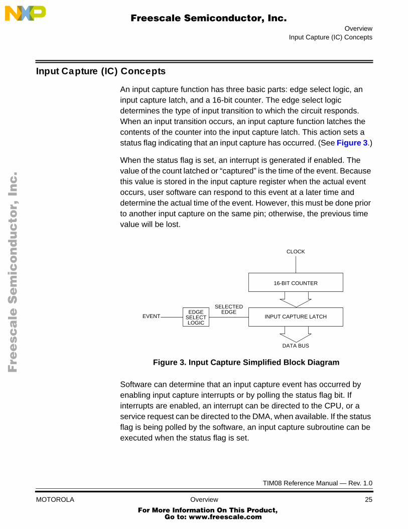
An input capture function has three basic parts: edge select logic, aninput capture latch, and a 16-bit counter. The edge select logicdetermines the type of input transition to which the circuit responds.When an input transition occurs, an input capture function latches thecontents of the counter into the input capture latch. This action sets astatus flag indicating that an input capture has occurred. (See Figure 3 .)
When the status flag is set, an interrupt is generated if enabled. Thevalue of the count latched or “captured” is the time of the event. Becausethis value is stored in the input capture register when the actual eventoccurs, user software can respond to this event at a later time anddetermine the actual time of the event. However, this must be done priorto another input capture on the same pin; otherwise, the previous timevalue will be lost.
Figure 3. Input Capture Simplified Block Diagram
Software can determine that an input capture event has occurred byenabling input capture interrupts or by polling the status flag bit. Ifinterrupts are enabled, an interrupt can be directed to the CPU, or aservice request can be directed to the DMA, when available. If the statusflag is being polled by the software, an input capture subroutine can beexecuted when the status flag is set.
CLOCK
16-BIT COUNTER
INPUT CAPTURE LATCH
DATA BUS
SELECTEDEDGEEDGE
SELECTLOGIC
EVENT
TIM08 Reference Manual — Rev. 1.0
MOTOROLA Overview 25 For More Information On This Product,
Go to: www.freescale.com
Overview
F
ree
sca
le S
em
ico
nd
uc
tor,
I
Freescale Semiconductor, Inc.n
c..
.
By recording the times for successive edges on an incoming signal,software can determine the period and/or pulse width of the signal. Tomeasure a period, two successive edges of the same polarity arecaptured. To measure a pulse width, two alternate polarity edges arecaptured. For example, to measure the high time of a pulse, the inputtransition is captured at the rising edge and subtracted from the timecaptured for the subsequent falling edge. When the period or pulse widthis less than the 16-bit modulo counter overflow period, the measurementis very straightforward. In practice, however, software usually must trackthe overflows of the 16-bit modulo counter to extend its range.
Another use for the input capture function is to establish a timereference. In this case, an input capture function is used in conjunctionwith an output compare function. For example, to activate an outputsignal, a specific number of clock cycles after detecting an input event(edge), use the input capture function to record the time at which theedge occurred. A number corresponding to the desired delay is addedto this captured value and stored to an output compare register.Because both input captures and output compares are referenced to thesame 16-bit modulo counter, the delay can be controlled to theresolution of the counter independent of software latencies.
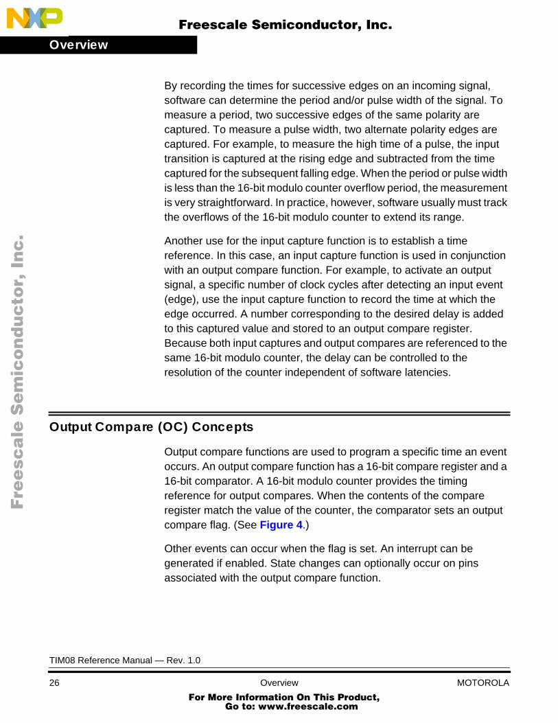
Output Compare (OC) Concepts
Output compare functions are used to program a specific time an eventoccurs. An output compare function has a 16-bit compare register and a16-bit comparator. A 16-bit modulo counter provides the timingreference for output compares. When the contents of the compareregister match the value of the counter, the comparator sets an outputcompare flag. (See Figure 4 .)
Other events can occur when the flag is set. An interrupt can begenerated if enabled. State changes can optionally occur on pinsassociated with the output compare function.
TIM08 Reference Manual — Rev. 1.0
26 Overview MOTOROLA For More Information On This Product,
Go to: www.freescale.com

OverviewOutput Compare (OC) Concepts
F
ree
sca
le S
em
ico
nd
uc
tor,
I
Freescale Semiconductor, Inc.n
c..
.
Figure 4. Output Compare Simplified Block Diagram
Software can determine that an output compare match has occurred byenabling output compare interrupts or by polling the status flag bit. Ifinterrupts are enabled, an interrupt can be directed to the CPU, or aservice request can be directed to the DMA, when available. If the statusflag is being polled by the software, an output compare subroutine canbe executed when the status flag is set.
The output compare function can generate an output of a specificduration and polarity. A 16-bit value corresponding to the time a pin statechange will occur is written to the output compare register. The outputcompare function is configured to automatically generate a high or lowoutput on the pin or toggle its state when the match occurs. The outputcompare register can be reprogrammed to a new value after thecompare occurs. The new value corresponds to the time the nextcompare occurs. When the next match takes place, the pin automaticallychanges to the specified state. The output compare pin can also beconfigured to toggle its state when the 16-bit modulo counter overflows.Because pin state changes occur automatically at specific values of thecounter, the pulse width can be controlled to the resolution of the counterindependent of software latencies. A periodic pulse of a specificfrequency and duty cycle can be generated by repeating the precedingsteps.
CLOCK
16-BIT COUNTER
16-BIT COMPARATOR16-BIT OUTPUT COMPAREREGISTER
=
OUTPUT MATCH
TIM08 Reference Manual — Rev. 1.0
MOTOROLA Overview 27 For More Information On This Product,
Go to: www.freescale.com

Overview
F
ree
sca
le S
em
ico
nd
uc
tor,
I
Freescale Semiconductor, Inc.n
c..
.
UnbufferedOutput Compares
Any TIM channel can generate unbuffered output compare pulses. Thesignal is unbuffered because changing the pulse width requires writingthe new pulse width value over the old value currently in the channelregisters.
An unsynchronized write to the channel registers to change a pulsewidth could cause incorrect operation for up to two counter periods. Forexample, if a new output compare value is written to the compareregisters before the previous output compare match occurred, but afterthe counter had reached the new value, no output compare match wouldoccur during that counter period. Or if a new, small value is written duringa timer overflow interrupt routine, but the output compare match ismissed because the new value is not written until after the timer counterhas passed that value, no output compare match would occur during thatcounter period.
The output compare interrupt occurs at the end of the current pulse,while the timer overflow interrupt occurs at the end of the current period.
In applications that cannot tolerate erroneous data during outputcompare pulse width changes, two methods are used to synchronize anunbuffered output compare pulse width. When changing to a longerpulse width, enable timer overflow interrupts and write the new pulsewidth during the timer overflow interrupt routine. When changing to ashorter pulse width, enable output compare interrupts and write the newpulse width value during the output compare interrupt routine.
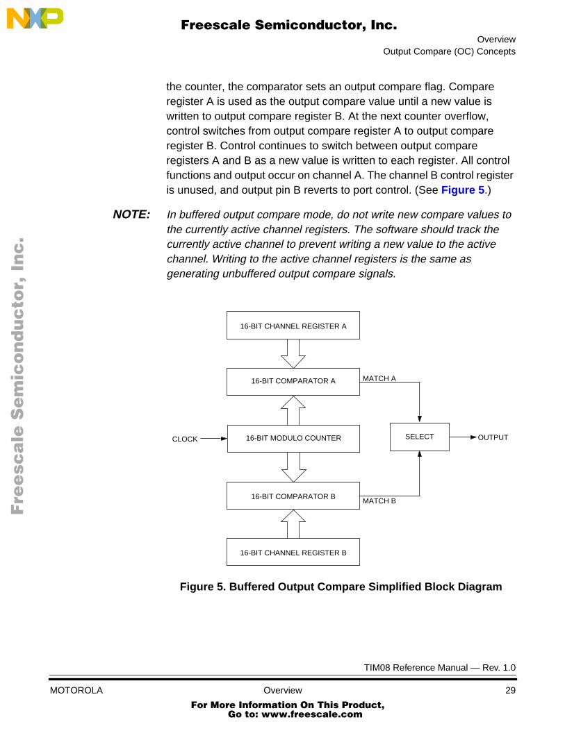
Buffered OutputCompares
A buffered output compare eliminates the synchronization probleminherent in the unbuffered output compare by providing two channelregisters in which to store compare values. In this method, the currentoutput compare value is contained in the first channel register, while anew output compare value is written into the second channel register.On counter overflow, the second channel register value is used togenerate the output compare match. By writing new output comparematch values only to the unused channel register, erroneous waveformscan be eliminated.
Two TIM channels can be linked to form one buffered output comparechannel. When the contents of compare register A match the value of
TIM08 Reference Manual — Rev. 1.0
28 Overview MOTOROLA For More Information On This Product,
Go to: www.freescale.com
OverviewOutput Compare (OC) Concepts
F
ree
sca
le S
em
ico
nd
uc
tor,
I
Freescale Semiconductor, Inc.n
c..
.
the counter, the comparator sets an output compare flag. Compareregister A is used as the output compare value until a new value iswritten to output compare register B. At the next counter overflow,control switches from output compare register A to output compareregister B. Control continues to switch between output compareregisters A and B as a new value is written to each register. All controlfunctions and output occur on channel A. The channel B control registeris unused, and output pin B reverts to port control. (See Figure 5 .)
NOTE: In buffered output compare mode, do not write new compare values tothe currently active channel registers. The software should track thecurrently active channel to prevent writing a new value to the activechannel. Writing to the active channel registers is the same asgenerating unbuffered output compare signals.
Figure 5. Buffered Output Compare Simplified Block Diagram
16-BIT CHANNEL REGISTER A
16-BIT COMPARATOR A
16-BIT COMPARATOR B
SELECT OUTPUTCLOCK
16-BIT CHANNEL REGISTER B
16-BIT MODULO COUNTER
MATCH A
MATCH B
TIM08 Reference Manual — Rev. 1.0
MOTOROLA Overview 29 For More Information On This Product,
Go to: www.freescale.com

Overview
F
ree
sca
le S
em
ico
nd
uc
tor,
I
Freescale Semiconductor, Inc.n
c..
.
Pulse-Width Modulation (PWM) Concepts
A pulse-width modulated waveform is created when the high to low timeratio, or pulse-width, of a periodic signal can be varied. For example, ifthe waveform can be incrementally changed by 1/256 of its period, it has8 bits of resolution. (See Figure 6 .)
Figure 6. Pulse-Width Modulation Example
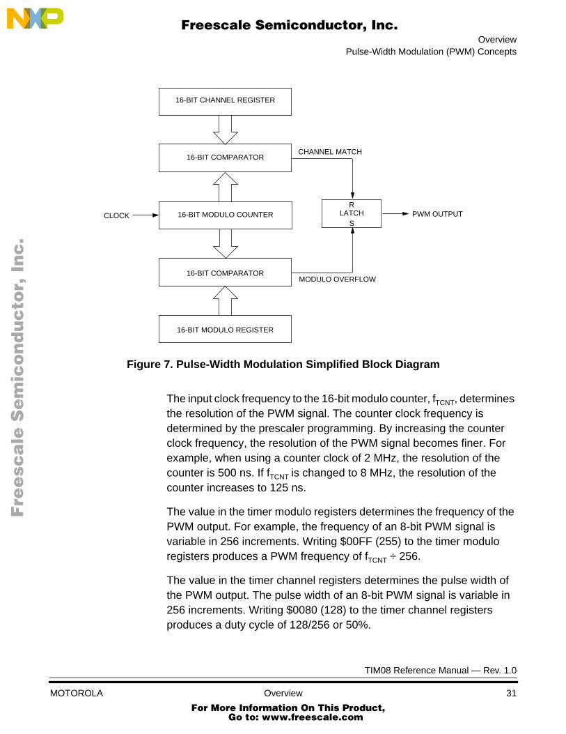
As shown in Figure 7 , a PWM function has a 16-bit counter, two 16-bitcomparators, and an output latch.
When the 16-bit counter reaches the modulo value in the 16-bit moduloregisters, the 16-bit modulo comparator sets the output latch, indicatinga modulo counter overflow. The modulo overflow is used as thereference to start the pulse, thereby setting the period of the waveform.As the counter is incremented, the counter value is compared with thecontents of the 16-bit channel register. When a match occurs the latchis reset, ending the pulse. The duty cycle of the signal is varied bychanging the value in the 16-bit channel register.
256 INCREMENTS
1/256
128/256
TIM08 Reference Manual — Rev. 1.0
30 Overview MOTOROLA For More Information On This Product,
Go to: www.freescale.com
OverviewPulse-Width Modulation (PWM) Concepts
F
ree
sca
le S
em
ico
nd
uc
tor,
I
Freescale Semiconductor, Inc.n
c..
.
Figure 7. Pulse-Width Modulation Simplified Block Diagram
The input clock frequency to the 16-bit modulo counter, fTCNT, determinesthe resolution of the PWM signal. The counter clock frequency isdetermined by the prescaler programming. By increasing the counterclock frequency, the resolution of the PWM signal becomes finer. Forexample, when using a counter clock of 2 MHz, the resolution of thecounter is 500 ns. If fTCNT is changed to 8 MHz, the resolution of thecounter increases to 125 ns.
The value in the timer modulo registers determines the frequency of thePWM output. For example, the frequency of an 8-bit PWM signal isvariable in 256 increments. Writing $00FF (255) to the timer moduloregisters produces a PWM frequency of fTCNT ÷ 256.
The value in the timer channel registers determines the pulse width ofthe PWM output. The pulse width of an 8-bit PWM signal is variable in256 increments. Writing $0080 (128) to the timer channel registersproduces a duty cycle of 128/256 or 50%.
16-BIT CHANNEL REGISTER
16-BIT COMPARATOR
16-BIT COMPARATOR
LATCH PWM OUTPUTCLOCKS
R
16-BIT MODULO REGISTER
16-BIT MODULO COUNTER
CHANNEL MATCH
MODULO OVERFLOW
TIM08 Reference Manual — Rev. 1.0
MOTOROLA Overview 31 For More Information On This Product,
Go to: www.freescale.com

Overview
F
ree
sca
le S
em
ico
nd
uc
tor,
I
Freescale Semiconductor, Inc.n
c..
.
The polarity of the pulse can be changed from a logic 1 state to a logic 0state. Writing to a special control bit is required to obtain a 100% dutycycle (output high all of the time) or a 0% duty cycle (output low all of thetime).
The PWM output can be used to electronically control the speed of amotor or the position of a servo. The PWM waveform drives an externalswitching amplifier which in turn controls the speed and direction of themotor. By adding a low-pass filter to a PWM output, the unit can be usedas a D/A converter. The longer the high time of the output waveform, thehigher the average value of output voltage produced. Other applicationsinclude data communication, where the pulse width indicates the datavalue.
Unbuffered PWMSignal Generation
Any TIM channel can generate unbuffered PWM signals. The signal isunbuffered because changing the pulse width requires writing the newpulse width value over the old value currently in the channel registers.
An unsynchronized write to the channel registers to change a pulsewidth could cause incorrect operation for up to two counter periods. Forexample, if a new pulse width value is written to the channel registersbefore the previous pulse width match occurred, but after the counterhad reached the new value, no pulse width match would occur duringthat counter period. Or if a new, small value is written during a timeroverflow interrupt routine, but the pulse width match is missed becausethe new value is not written until after the timer counter is past that value,no pulse width match would occur during that counter period.
The PWM interrupt occurs at the end of the current pulse. The timeroverflow interrupt, by contrast, occurs at the end of the current period.
In applications which cannot tolerate erroneous data during outputcompare pulse width changes, two methods are used to synchronize anunbuffered PWM pulse width. When changing to a longer pulse width,enable timer overflow interrupts and writes the new pulse width duringthe timer overflow interrupt routine. When changing to a shorter pulsewidth, enable PWM interrupts and writes the new pulse width valueduring the PWM interrupt routine.
TIM08 Reference Manual — Rev. 1.0
32 Overview MOTOROLA For More Information On This Product,
Go to: www.freescale.com
OverviewPulse-Width Modulation (PWM) Concepts
F
ree
sca
le S
em
ico
nd
uc
tor,
I
Freescale Semiconductor, Inc.n
c..
.
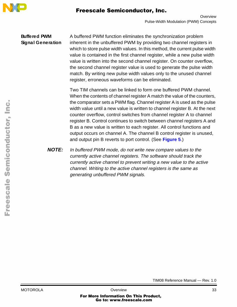
Buffered PWMSignal Generation
A buffered PWM function eliminates the synchronization probleminherent in the unbuffered PWM by providing two channel registers inwhich to store pulse width values. In this method, the current pulse widthvalue is contained in the first channel register, while a new pulse widthvalue is written into the second channel register. On counter overflow,the second channel register value is used to generate the pulse widthmatch. By writing new pulse width values only to the unused channelregister, erroneous waveforms can be eliminated.
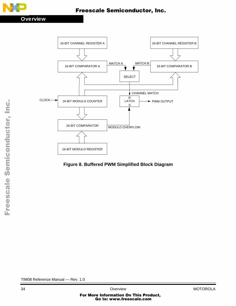
Two TIM channels can be linked to form one buffered PWM channel.When the contents of channel register A match the value of the counters,the comparator sets a PWM flag. Channel register A is used as the pulsewidth value until a new value is written to channel register B. At the nextcounter overflow, control switches from channel register A to channelregister B. Control continues to switch between channel registers A andB as a new value is written to each register. All control functions andoutput occurs on channel A. The channel B control register is unused,and output pin B reverts to port control. (See Figure 5 .)
NOTE: In buffered PWM mode, do not write new compare values to thecurrently active channel registers. The software should track thecurrently active channel to prevent writing a new value to the activechannel. Writing to the active channel registers is the same asgenerating unbuffered PWM signals.
TIM08 Reference Manual — Rev. 1.0
MOTOROLA Overview 33 For More Information On This Product,
Go to: www.freescale.com
Overview
F
ree
sca
le S
em
ico
nd
uc
tor,
I
Freescale Semiconductor, Inc.n
c..
.
Figure 8. Buffered PWM Simplified Block Diagram
16-BIT CHANNEL REGISTER A
16-BIT COMPARATOR A
16-BIT COMPARATOR
SELECT
CHANNEL MATCH
CLOCK
16-BIT MODULO REGISTER
16-BIT MODULO COUNTER
MATCH A
MODULO OVERFLOW
LATCH PWM OUTPUTS
R
MATCH B
16-BIT CHANNEL REGISTER B
16-BIT COMPARATOR B
TIM08 Reference Manual — Rev. 1.0
34 Overview MOTOROLA For More Information On This Product,
Go to: www.freescale.com

F
ree
sca
le S
em
ico
nd
uc
tor,
IFreescale Semiconductor, Inc.
nc
...
Signal Description
Contents
Introduction . . . . . . . . . . . . . . . . . . . . . . . . . . . . . . . . . . . . . . . . . . . . .35
Signal Groups . . . . . . . . . . . . . . . . . . . . . . . . . . . . . . . . . . . . . . . . . . .36
Input Capture/Output Compare Pins (TCH0, TCH1, TCH2, TCH3) . .36Input Capture Pins . . . . . . . . . . . . . . . . . . . . . . . . . . . . . . . . . . . .37Output Compare Pins . . . . . . . . . . . . . . . . . . . . . . . . . . . . . . . . . .37PWM Output Pins . . . . . . . . . . . . . . . . . . . . . . . . . . . . . . . . . . . . .37General Purpose I/O . . . . . . . . . . . . . . . . . . . . . . . . . . . . . . . . . . .37
Auxiliary Timer Clock Input (TCLK) . . . . . . . . . . . . . . . . . . . . . . . . . .38
Introduction
The TIM has five signal pins that provide connections to the internalfunctions of the module. These pins are shared with port pins on themicrocontroller. This section contains brief descriptions of the TIM inputand output signals in their functional groups. See ElectricalSpecifications for timing information for these signals.
NOTE: The TIM can be implemented with two, four, six or eight channels. Thismanual will show the 4-channel version, as implemented in theMC68HC708XL36.
TIM08 Reference Manual — Rev. 1.0
MOTOROLA Signal Description 35 For More Information On This Product,
Go to: www.freescale.com

Signal Description
F
ree
sca
le S
em
ico
nd
uc
tor,
I
Freescale Semiconductor, Inc.n
c..
.
Signal Groups
The block diagram in Figure 9 shows the signal pins. When the pins arenot needed for their TIM function, they can be used for general-purposeinput or output as part of a parallel data port. The port pins are part of aseparate module. Refer to the applicable technical data book forinformation on the port module associated with the TIM. The blockdiagram also shows which TIM signals are bidirectional and which areeither input or output only.
Figure 9. Function Signal Groups
Input Capture/Output Compare Pins (TCH0, TCH1, TCH2, TCH3)
Each of these pins is dedicated to one of the timer channels. These pinscan be configured for an input capture, output compare, or PWMfunction. Each channel pin has one 16-bit register, which is used forholding either the input capture value or the output compare/PWM matchvalue. When used as an input, the signal is conditioned so that any pulselonger than one bus clock period is guaranteed to pass. If this pin is notneeded for either the input capture, output compare, or PWM function, itcan be used for general-purpose I/O.
CAPTURE/COMPARE UNIT
16-BIT COUNTER
TCLK
TCH0
TCH1
TCH2
PRESCALER
TCH3
EXTERNAL INTERNALMCU BUSMCU BUS
PORT PIN
PORT PIN
PORT PIN
PORT PIN
PORT PIN
TIM08 Reference Manual — Rev. 1.0
36 Signal Description MOTOROLA For More Information On This Product,
Go to: www.freescale.com

Signal DescriptionInput Capture/Output Compare Pins (TCH0, TCH1, TCH2, TCH3)
F
ree
sca
le S
em
ico
nd
uc
tor,
I
Freescale Semiconductor, Inc.n
c..
.
Input Capture Pins With the input capture function, the TIM can capture the time at which anexternal event occurs. When an active edge occurs on the pin of an inputcapture channel, the TIM latches the contents of the timer counter intothe channel registers, TCHxH:TCHxL. The polarity of the active edge isprogrammable. Input captures can generate CPU interrupts or DMAservice requests on microcontrollers with a DMA module.
See Input Capture (IC) Functions for information on the operation ofthis function.
OutputCompare Pins
With the output compare function, the TIM can generate an output signalat programmable intervals. When the counter reaches the value in theregisters of an output compare channel, the TIM can set, clear, or togglethe channel pin. Output compares can generate CPU interrupts or DMAservice requests on microcontrollers with a DMA module.
See Unbuffered Output Compare (OC) Functions and BufferedOutput Compare (OC) Functions for information on the operation ofthese functions.
PWMOutput Pins
With the PWM function, the TIM can generate a pulse-width modulatedoutput signal. When the counter reaches the value in the registers of aPWM channel, the TIM can set, clear, or toggle the channel pin. A PWMfunction can generate CPU interrupts or DMA service requests onmicrocontrollers with a DMA module.
See Unbuffered Pulse Width Modulation (PWM) Functions andBuffered Pulse Width Modulation (PWM) Functions for informationon the operation of these functions.
General-PurposeI/O
If not used as input capture, output compare, or PWM functions, thesepins may be used as general-purpose I/O. This is accomplished byclearing the ELSxB and ELSxA bits in the TSCx register for eachchannel pin, as described in Capture/Compare Unit . Refer to theapplicable technical data book for more information about using thesepins as bidirectional I/O pins.
TIM08 Reference Manual — Rev. 1.0
MOTOROLA Signal Description 37 For More Information On This Product,
Go to: www.freescale.com

Signal Description
F
ree
sca
le S
em
ico
nd
uc
tor,
I
Freescale Semiconductor, Inc.n
c..
.
Auxiliary Timer Clock Input (TCLK)
TCLK is an external clock input that can be used as the clock source forthe timer counter instead of the prescaled bus clock. Any TCLK pulselonger than one bus clock period is guaranteed to pass. See Prescalerfor additional information on TCLK.
If this pin is not used as a clock input, it can be used as a general-purpose I/O pin. See Table 1 for information on selecting the function ofthis pin. The minimum TCLK pulse width, TCLKLMIN or TCLKHMIN, is:
The maximum TCLK frequency is:
PTE3/TCLK is available as a general-purpose I/O pin when not used asthe TIM clock input. When the PTE3/TCLK pin is the TIM clock input, itis an input regardless of the state of the DDRE3 bit in data directionregister E.
bus frequency1
+ tsu
bus frequency2
TIM08 Reference Manual — Rev. 1.0
38 Signal Description MOTOROLA For More Information On This Product,
Go to: www.freescale.com

F
ree
sca
le S
em
ico
nd
uc
tor,
IFreescale Semiconductor, Inc.
nc
...
Prescaler
Contents
Introduction . . . . . . . . . . . . . . . . . . . . . . . . . . . . . . . . . . . . . . . . . . . . .39
Prescaler . . . . . . . . . . . . . . . . . . . . . . . . . . . . . . . . . . . . . . . . . . . . . .40
Timer Status and Control Register (TSC) . . . . . . . . . . . . . . . . . . . . . .41
Introduction
The TIM has its own 16-bit counter as the main timing component. Thiscounter clock is derived from the prescaler or the external input pinTCLK.
TIM08 Reference Manual — Rev. 1.0
MOTOROLA Prescaler 39 For More Information On This Product,
Go to: www.freescale.com
Prescaler
F
ree
sca
le S
em
ico
nd
uc
tor,
I
Freescale Semiconductor, Inc.n
c..
.
Prescaler
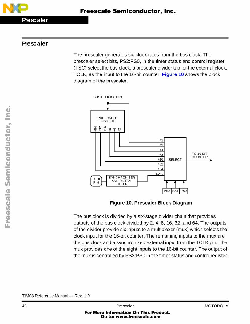
The prescaler generates six clock rates from the bus clock. Theprescaler select bits, PS2:PS0, in the timer status and control register(TSC) select the bus clock, a prescaler divider tap, or the external clock,TCLK, as the input to the 16-bit counter. Figure 10 shows the blockdiagram of the prescaler.
Figure 10. Prescaler Block Diagram
The bus clock is divided by a six-stage divider chain that providesoutputs of the bus clock divided by 2, 4, 8, 16, 32, and 64. The outputsof the divider provide six inputs to a multiplexer (mux) which selects theclock input for the 16-bit counter. The remaining inputs to the mux arethe bus clock and a synchronized external input from the TCLK pin. Themux provides one of the eight inputs to the 16-bit counter. The output ofthe mux is controlled by PS2:PS0 in the timer status and control register.
DIVIDER
BUS CLOCK (IT12)
TO 16-BITCOUNTER
SELECT
SYNCHRONIZERAND DIGITAL
FILTER
TCLKPIN
÷2÷4÷8÷16
÷32
÷64
÷4
÷8
÷16
÷32
÷64
EXT.
÷2
PS2 PS1 PS0
÷1
PRESCALER
TIM08 Reference Manual — Rev. 1.0
40 Prescaler MOTOROLA For More Information On This Product,
Go to: www.freescale.com

PrescalerTimer Status and Control Register
F
ree
sca
le S
em
ico
nd
uc
tor,
I
Freescale Semiconductor, Inc.n
c..
.
TCLK is an external clock input. TCLK can be used as the clock sourcefor the 16-bit counter instead of the bus clock or its derivative. Figure 11shows the timing of TCLK and its synchronization to the bus clock.
Figure 11. TCLK Timing
where
Timer Status and Control Register
Figure 12. Timer Status and Control Register (TSC)
TOF — Unused in prescaler; see Timer Status and Control Registerfor description.
TOE — Unused in prescaler; see Timer Status and Control Registerfor description.
IT12 — BUS CLOCK
TCLK
COUNTER CLOCK
⇑ ⇓ ⇑⇑⇓
ONE BUS CLOCK
tcyc =1
bus frequency + tsu
TSC Bit 7 6 5 4 3 2 1 Bit 0
Read: TOFTOE TSTOP
0 0PS2 PS1 PS0
Write: 0 TRST
Reset: 0 0 1 0 0 0 0 0
Shading indicates this bit is not used in the prescaler section.
TIM08 Reference Manual — Rev. 1.0
MOTOROLA Prescaler 41 For More Information On This Product,
Go to: www.freescale.com

Prescaler
F
ree
sca
le S
em
ico
nd
uc
tor,
I
Freescale Semiconductor, Inc.n
c..
.
Figure 13. TSTOP Timing
COUNTER CLOCK = BUS CLOCK (IT12)
IT12
INTERNAL
INTERNAL
TCNTH:L 0000 0001 0002 0003 0004
W§ W§R§INTERNAL
TSTOP
COUNTER(PS2:PS0=000)
WRITE TSTOP = 0
W‡ W‡
W† W†
R‡
R†
WRITE TSTOP = 1
*
R†W† WRITE DATA
READ DATAR‡W‡ WRITE ADDRESS
READ ADDRESS R§ READW§ WRITE
READ/WRITE IS NOT USUALLY IN BACK-TO-BACK CYCLES.*
COUNTER CLOCK = IT12 ÷ 4
0000 0001 0002
IT12
INTERNAL
INTERNAL
COUNTER
TSTOP
TCNTH:L
W‡ W‡
WRITE TSTOP = 0 WRITE TSTOP = 1
W‡ W‡
* *
ADDRESS BUS
DATA BUS
READ/WRITE
CLOCK
ADDRESS BUS
READ/WRITE
CLOCK
INTERNALW† W†DATA BUS
TIM08 Reference Manual — Rev. 1.0
42 Prescaler MOTOROLA For More Information On This Product,
Go to: www.freescale.com
PrescalerTimer Status and Control Register
F
ree
sca
le S
em
ico
nd
uc
tor,
I
Freescale Semiconductor, Inc.n
c..
.
TSTOP — Timer stop
This read/write bit stops the timer counter. Counting resumes whenTSTOP is cleared. Reset sets the TSTOP bit, stopping the timercounter until the TIM is enabled.
1 = Timer counter stopped0 = Timer counter active
To preserve the correct timing relationship, TSTOP stops the inputclock to the prescaler. The relationship cannot be preserved whenusing the external TCLK as the counter clock. Figure 13 for details onthe timing of the TSTOP function.
TRST — Timer reset
Setting this write-only bit resets the timer counter and the timerprescaler. Setting TRST has no effect on any other registers.Counting resumes from $0000. TRST is cleared automatically afterthe timer counter is reset, and always reads 0. Reset clears the TRSTbit.
1 = Prescaler and timer counter cleared0 = No effect
See Figure 14 for details on the timing of the TRST function.
NOTE: Setting the TSTOP and TRST bits simultaneously stops the timercounter at a value of $0000.
Bit 3 — Not used; always reads 0.
TIM08 Reference Manual — Rev. 1.0
MOTOROLA Prescaler 43 For More Information On This Product,
Go to: www.freescale.com

Prescaler
F
ree
sca
le S
em
ico
nd
uc
tor,
I
Freescale Semiconductor, Inc.n
c..
.
Figure 14. TRST Timing
TCNTH:L 0014 0015 0000 0001 0002
WRITE TRST = 1
COUNTER CLOCK = BUS CLOCK (IT12)
IT12
INTERNAL
INTERNAL
W§INTERNAL
W‡
W†
COUNTER
(PS2:PS0=000)
R†W† WRITE DATA
READ DATAR‡W‡ WRITE ADDRESS
READ ADDRESS R§ READW§ WRITE
READ/WRITE IS NOT USUALLY IN BACK-TO-BACK CYCLES.*
0005 0006 00000004 0001
COUNTER
TCNTH:L
WRITE TRST = 1
IT12
INTERNAL
INTERNAL
W†
W‡
COUNTER CLOCK = IT12 ÷ 4
ADDRESS BUS
DATA BUS
READ/WRITE
CLOCK
0003
CLOCK
DATA BUS
ADDRESS BUS
INTERNALW§READ/WRITE
TIM08 Reference Manual — Rev. 1.0
44 Prescaler MOTOROLA For More Information On This Product,
Go to: www.freescale.com

PrescalerTimer Status and Control Register
F
ree
sca
le S
em
ico
nd
uc
tor,
I
Freescale Semiconductor, Inc.n
c..
.
PS2:PS0 — Prescaler bits
These read/write bits select the bus clock, one of the six prescaleroutputs, or the TCLK pin as the input to the timer counter. Table 1shows the prescaler selection encoding, including the TIM clocksource, and the function of the TCLK pin. Reset clears the PS2:PS0bits.
NOTE: Stop the TIM before changing the prescaler output. Before writing to theprescaler select bits (PS2:PS0), set the timer stop bit (TSTOP).
NOTE: Changing the prescaler control bits while the TIM is running may causean extra count if the input clock previously selected was a logic level 0and the new input clock logic level is 1.
Refer to Stop Mode for information on stopping the prescaler.
Table 1. Prescaler Selection
PS2:1:0 TIM Clock Source PORT/TCLKFunction
000 Bus Clock PORT
001 Bus Clock ÷ 2 PORT
010 Bus Clock ÷ 4 PORT
011 Bus Clock ÷ 8 PORT
100 Bus Clock ÷ 16 PORT
101 Bus Clock ÷ 32 PORT
110 Bus Clock ÷ 64 PORT
111 TCLK TCLK
TIM08 Reference Manual — Rev. 1.0
MOTOROLA Prescaler 45 For More Information On This Product,
Go to: www.freescale.com

Prescaler
F
ree
sca
le S
em
ico
nd
uc
tor,
I
Freescale Semiconductor, Inc.n
c..
.
TIM08 Reference Manual — Rev. 1.0
46 Prescaler MOTOROLA For More Information On This Product,
Go to: www.freescale.com

F
ree
sca
le S
em
ico
nd
uc
tor,
IFreescale Semiconductor, Inc.
nc
...
16-Bit Modulo Counter
Contents
Introduction . . . . . . . . . . . . . . . . . . . . . . . . . . . . . . . . . . . . . . . . . . . . .47
Timer Counter . . . . . . . . . . . . . . . . . . . . . . . . . . . . . . . . . . . . . . . . . . .47
Timer Status and Control Register . . . . . . . . . . . . . . . . . . . . . . . . . . .49
Timer Counter Registers . . . . . . . . . . . . . . . . . . . . . . . . . . . . . . . . . .53
Timer Counter Modulo Registers . . . . . . . . . . . . . . . . . . . . . . . . . . . .54
Introduction
The timer counter provides the capture/compare units with a counterreference for the input capture (IC) functions, the output compare (OC)functions, and the pulse-width modulation (PWM) functions.
Timer Counter
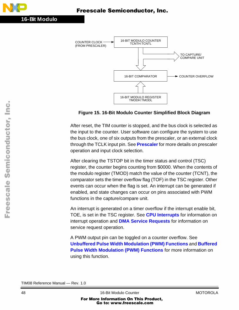
The timer counter (TCNT) is the key timing component for thecapture/compare unit. The timer counter is a 16-bit modulo counter witha programmable input clock and the capability to be stopped or reset bymanipulating control bits in the timer status and control register. The16-bit modulo counter consists of a 16-bit counter, a 16-bit comparator,a 16-bit modulo register, and interrupt generation logic. Refer to Figure15.
TIM08 Reference Manual — Rev. 1.0
MOTOROLA 16-Bit Modulo Counter 47 For More Information On This Product,
Go to: www.freescale.com
16-Bit Modulo
F
ree
sca
le S
em
ico
nd
uc
tor,
I
Freescale Semiconductor, Inc.n
c..
.
Figure 15. 16-Bit Modulo Counter Simplified Block Diagram
After reset, the TIM counter is stopped, and the bus clock is selected asthe input to the counter. User software can configure the system to usethe bus clock, one of six outputs from the prescaler, or an external clockthrough the TCLK input pin. See Prescaler for more details on prescaleroperation and input clock selection.
After clearing the TSTOP bit in the timer status and control (TSC)register, the counter begins counting from $0000. When the contents ofthe modulo register (TMOD) match the value of the counter (TCNT), thecomparator sets the timer overflow flag (TOF) in the TSC register. Otherevents can occur when the flag is set. An interrupt can be generated ifenabled, and state changes can occur on pins associated with PWMfunctions in the capture/compare unit.
An interrupt is generated on a timer overflow if the interrupt enable bit,TOE, is set in the TSC register. See CPU Interrupts for information oninterrupt operation and DMA Service Requests for information onservice request operation.
A PWM output pin can be toggled on a counter overflow. SeeUnbuffered Pulse Width Modulation (PWM) Functions and BufferedPulse Width Modulation (PWM) Functions for more information onusing this function.
16-BIT COMPARATOR
COUNTER CLOCK
16-BIT MODULO REGISTER
16-BIT MODULO COUNTER
(FROM PRESCALER)
TO CAPTURE/
COUNTER OVERFLOW
TMODH:TMODL
TCNTH:TCNTL
COMPARE UNIT
TIM08 Reference Manual — Rev. 1.0
48 16-Bit Modulo Counter MOTOROLA For More Information On This Product,
Go to: www.freescale.com

16-Bit Modulo CounterTimer Status and Control Register
F
ree
sca
le S
em
ico
nd
uc
tor,
I
Freescale Semiconductor, Inc.n
c..
.
Timer Status and Control Register
Figure 16. Timer Status and Control Register (TSC)
TOF — Timer Overflow Flag
This clearable flag is set when the timer counter reaches the modulovalue programmed in the timer modulo registers. Clear TOF byreading the timer status and control register when TOF is set and thenwriting a 0 to TOF. If another timer overflow occurs before the clearingsequence is complete, then writing 0 to TOF has no effect. Therefore,a TOF interrupt request cannot be lost due to inadvertent clearing ofTOF. Writing a 1 to this bit has no effect. Reset clears the TOF bit.
1 = Timer counter has reached modulo value.0 = Timer counter has not reached modulo value.
TOE — Timer Overflow Enable
This read/write bit enables timer overflow interrupts when the TOF bitbecomes set. Reset clears the TOE bit.
1 = Timer overflow interrupts enabled0 = Timer overflow interrupts disabled
TSTOP — Timer STOP
This read/write bit stops the timer counter. Counting resumes whenTSTOP is cleared. Reset sets the TSTOP bit, stopping the timercounter until the TIM is enabled.
1 = Timer counter stopped0 = Timer counter active
To preserve the correct timing relationship, TSTOP stops the inputclock to the prescaler. The relationship cannot be preserved when
TSC Bit 7 6 5 4 3 2 1 Bit 0
Read: TOFTOE TSTOP
0 0PS2 PS1 PS0
Write: 0 TRST
Reset: 0 0 1 0 0 0 0 0
Shading indicates this bit is not used in the counter section.
TIM08 Reference Manual — Rev. 1.0
MOTOROLA 16-Bit Modulo Counter 49 For More Information On This Product,
Go to: www.freescale.com

16-Bit Modulo
F
ree
sca
le S
em
ico
nd
uc
tor,
I
Freescale Semiconductor, Inc.n
c..
.
using the external TCLK as the counter clock. Refer to Figure 17 fordetails on the timing of the TSTOP function.
NOTE: Do not set the TSTOP bit before entering wait mode if the TIM is requiredto exit wait mode.
Figure 17. TSTOP Timing
COUNTER CLOCK = BUS CLOCK (IT12)
IT12
INTERNAL
INTERNAL
TCNTH:L 0000 0001 0002 0003 0004
W§ W§R§INTERNAL
TSTOP
COUNTER (PS2:PS0=000)
WRITE TSTOP = 0
W‡ W‡
W† W†
R‡
R†
WRITE TSTOP = 1
*
R†W† WRITE DATA
READ DATAR‡W‡ WRITE ADDRESS
READ ADDRESS R§ READW§ WRITE
READ/WRITE IS NOT USUALLY IN BACK-TO-BACK CYCLES.*
COUNTER CLOCK = IT12 ÷ 4
0000 0001 0002
IT12
INTERNAL
INTERNAL
COUNTER
TSTOP
TCNTH:L
W‡ W‡
WRITE TSTOP = 0 WRITE TSTOP = 1
W‡ W‡
* *
ADDRESS BUS
DATA BUS
READ/WRITE
CLOCK
ADDRESS BUS
READ/WRITE
CLOCK
INTERNALW† W†DATA BUS
TIM08 Reference Manual — Rev. 1.0
50 16-Bit Modulo Counter MOTOROLA For More Information On This Product,
Go to: www.freescale.com

16-Bit Modulo CounterTimer Status and Control Register
F
ree
sca
le S
em
ico
nd
uc
tor,
I
Freescale Semiconductor, Inc.n
c..
.
TRST — Timer reset
Setting this write-only bit resets the timer counter and the timerprescaler. Setting TRST has no effect on any other registers.Counting resumes from $0000. TRST is cleared automatically afterthe timer counter is reset, and always reads 0. Reset clears the TRSTbit.
1 = Prescaler and timer counter cleared0 = No effect
See Figure 18 for details on the timing of the TRST function.
NOTE: Setting the TSTOP and TRST bits simultaneously stops the timercounter at a value of $0000.
PS2:PS0 — Unused in counter; see Timer Status and ControlRegister for a description.
TIM08 Reference Manual — Rev. 1.0
MOTOROLA 16-Bit Modulo Counter 51 For More Information On This Product,
Go to: www.freescale.com

16-Bit Modulo
F
ree
sca
le S
em
ico
nd
uc
tor,
I
Freescale Semiconductor, Inc.n
c..
.
Figure 18. TRST Timing
TCNTH:L 0014 0015 0000 0001 0002
WRITE TRST = 1
COUNTER CLOCK = BUS CLOCK (IT12)
IT12
INTERNAL
INTERNAL
W§INTERNAL
W‡
W†
COUNTER
(PS2:PS0=000)
R†W† WRITE DATA
READ DATAR‡W‡ WRITE ADDRESS
READ ADDRESS R§ READW§ WRITE
READ/WRITE IS NOT USUALLY IN BACK-TO-BACK CYCLES.*
0005 0006 00000004 0001
COUNTER
TCNTH:L
WRITE TRST = 1
IT12
INTERNAL
INTERNAL
W†
W‡
COUNTER CLOCK = IT12 ÷ 4
ADDRESS BUS
DATA BUS
READ/WRITE
CLOCK
0003
CLOCK
DATA BUS
ADDRESS BUS
INTERNALW§READ/WRITE
TIM08 Reference Manual — Rev. 1.0
52 16-Bit Modulo Counter MOTOROLA For More Information On This Product,
Go to: www.freescale.com
16-Bit Modulo CounterTimer Counter Registers
F
ree
sca
le S
em
ico
nd
uc
tor,
I
Freescale Semiconductor, Inc.n
c..
.
Timer Counter Registers
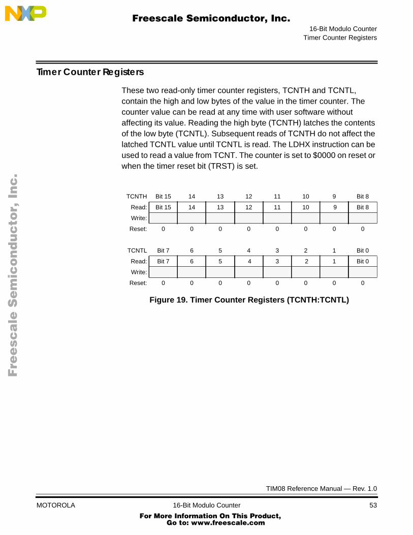
These two read-only timer counter registers, TCNTH and TCNTL,contain the high and low bytes of the value in the timer counter. Thecounter value can be read at any time with user software withoutaffecting its value. Reading the high byte (TCNTH) latches the contentsof the low byte (TCNTL). Subsequent reads of TCNTH do not affect thelatched TCNTL value until TCNTL is read. The LDHX instruction can beused to read a value from TCNT. The counter is set to $0000 on reset orwhen the timer reset bit (TRST) is set.
Figure 19. Timer Counter Registers (TCNTH:TCNTL)
TCNTH Bit 15 14 13 12 11 10 9 Bit 8
Read: Bit 15 14 13 12 11 10 9 Bit 8
Write:
Reset: 0 0 0 0 0 0 0 0
TCNTL Bit 7 6 5 4 3 2 1 Bit 0
Read: Bit 7 6 5 4 3 2 1 Bit 0
Write:
Reset: 0 0 0 0 0 0 0 0
TIM08 Reference Manual — Rev. 1.0
MOTOROLA 16-Bit Modulo Counter 53 For More Information On This Product,
Go to: www.freescale.com

16-Bit Modulo
F
ree
sca
le S
em
ico
nd
uc
tor,
I
Freescale Semiconductor, Inc.n
c..
.
Timer Counter Modulo Registers
These two read/write timer counter modulo registers, TMODH andTMODL, contain the high and low bytes of the modulo value for the timercounter. When the timer counter reaches the modulo value, the TOF flagis automatically set by hardware, and the timer counter resumescounting from $0000 at the next clock. The overflow flag (TOF) andoverflow interrupts are inhibited after a write to the high byte (TMODH)until the low byte (TMODL) is written. The STHX instruction can be usedto write values to TMOD, and the LDHX instruction can be used to readvalues from TMOD. Reset sets the timer counter modulo registers to$FFFF, enabling the modulo counter to act as a free-running counter.
Figure 20. Timer Counter Modulo Registers (TMODH:TMODL)
NOTE: If TMODH:TMODL is set to $0000, a TOF is generated on the first cyclein which the match occurs, but not subsequently.
NOTE: Stop and reset the timer counter before writing to the timer countermodulo registers.
TMODH Bit 15 14 13 12 11 10 9 Bit 8
Read:Bit 15 14 13 12 11 10 9 Bit 8
Write:
Reset: 1 1 1 1 1 1 1 1
TMODL Bit 7 6 5 4 3 2 1 Bit 0
Read:Bit 7 6 5 4 3 2 1 Bit 0
Write:
Reset: 1 1 1 1 1 1 1 1
TIM08 Reference Manual — Rev. 1.0
54 16-Bit Modulo Counter MOTOROLA For More Information On This Product,
Go to: www.freescale.com

F
ree
sca
le S
em
ico
nd
uc
tor,
IFreescale Semiconductor, Inc.
nc
...
Capture/Compare Unit
Contents
Introduction . . . . . . . . . . . . . . . . . . . . . . . . . . . . . . . . . . . . . . . . . . . . .56
Input Capture (IC) Functions . . . . . . . . . . . . . . . . . . . . . . . . . . . . . . .57Timer Channel Status and Control Registers . . . . . . . . . . . . . . . .60Timer Channel Registers . . . . . . . . . . . . . . . . . . . . . . . . . . . . . . .63
Unbuffered Output Compare (OC) Functions . . . . . . . . . . . . . . . . . . .65Timer Channel Status and Control Registers . . . . . . . . . . . . . . . .67Timer Channel Registers . . . . . . . . . . . . . . . . . . . . . . . . . . . . . . .70
Buffered Output Compare (OC) Functions . . . . . . . . . . . . . . . . . . . . .72
Timer Channel Status and Control Registers . . . . . . . . . . . . . . . . . . .75Timer Channel Registers . . . . . . . . . . . . . . . . . . . . . . . . . . . . . . .78
Unbuffered Pulse Width Modulation (PWM) Functions . . . . . . . . . . .80Timer Channel Status and Control Registers . . . . . . . . . . . . . . . .83Timer Channel Registers . . . . . . . . . . . . . . . . . . . . . . . . . . . . . . .88
Buffered Pulse Width Modulation (PWM) Functions . . . . . . . . . . . . .90Timer Channel Status and Control Registers . . . . . . . . . . . . . . . .94Timer Channel Registers . . . . . . . . . . . . . . . . . . . . . . . . . . . . . . .98
TIM08 Reference Manual — Rev. 1.0
MOTOROLA Capture/Compare Unit 55 For More Information On This Product,
Go to: www.freescale.com

Capture/Compare Unit
F
ree
sca
le S
em
ico
nd
uc
tor,
I
Freescale Semiconductor, Inc.n
c..
.
Introduction
The capture/compare unit is one of the major submodules of the TIM. Itcontains the input capture (IC) functions, the output compare (OC)functions, and the pulse-width modulation (PWM) functions.
The function provided by each of the channels is determined by theconfiguration of the status and control register for each channel. Thefollowing sections describe how to set up the status and control registersto generate IC functions, unbuffered and buffered OC functions, andunbuffered and buffered PWM functions. See Input Capture (IC)Concepts , Output Compare (OC) Concepts , and Pulse-WidthModulation (PWM) Concepts for more information about thesefunctions.
NOTE: The TIM can be implemented with two, four, six or eight channels. Thismanual will show the 4-channel version, as implemented in theMC68HC708XL36.
TIM08 Reference Manual — Rev. 1.0
56 Capture/Compare Unit MOTOROLA For More Information On This Product,
Go to: www.freescale.com
Capture/Compare UnitInput Capture (IC) Functions
F
ree
sca
le S
em
ico
nd
uc
tor,
I
Freescale Semiconductor, Inc.n
c..
.
Input Capture (IC) Functions
Each TIM input capture pin TCH0–TCH3, when used as an input capturefunction, has a 16-bit register latch (TCHxH/L), inputedge-detection/selection logic, and interrupt synchronization/generationlogic. All of the input capture functions use the same 16-bit timer counter(TCNT). The latch captures the contents of the TCNT when the selectedevent occurs at the corresponding input capture pin.
See Input Capture (IC) Concepts for additional information on thebasic operation of an input capture function.
The edge detection logic contains control bits that allow user software toselect the edge polarity to be recognized. These are the ELSxB andELSxA bits in the timer status and control register (TSCx). Each of theinput capture functions can be independently configured to detect risingedges only, falling edges only, any edge (rising or falling), or disable theinput capture function. Table 2 for the required bit patterns.
The input capture functions operate independently of each other and cancapture the same TCNT value if the input edges are all detected withinthe same timer count cycle.
The interrupt generation logic includes a status flag, which indicates thatan edge is detected, and a local interrupt enable bit, which determines ifthe corresponding input capture function will generate an interrupt orservice request. The input capture sets the CHxF bit in the TSCx and cancause an interrupt or service request if the corresponding CHxIE bit isset in the TSCx. If the interrupt is disabled (CHxIE = 0), the input captureis operating in polled mode where software must read the status flag torecognize that an edge was detected. Refer to CPU Interrupts foradditional details on interrupt operation and DMA Service Requests foradditional details on service request operation.
Because input capture events are generally asynchronous to the timercounter, they are synchronized to the bus clock so that actual latching ofthe TCNT contents occurs just after the counter increments. The input isconditioned in such a way that any event longer than one bus clock isguaranteed to be captured. The relationship of the bus clock to the
TIM08 Reference Manual — Rev. 1.0
MOTOROLA Capture/Compare Unit 57 For More Information On This Product,
Go to: www.freescale.com

Capture/Compare Unit
F
ree
sca
le S
em
ico
nd
uc
tor,
I
Freescale Semiconductor, Inc.n
c..
.
output of the synchronizer is shown in Figure 21 . The value latched intothe timer channel register by an input capture corresponds to the valueof the counter one bus clock cycle after the input transition that triggeredthe edge detection logic. There can be up to one bus clock cycle ofuncertainty in latching of the input transition. The maximum time isdetermined by the bus clock frequency, fOP.
Figure 21. Input Capture Timing
NAME DESCRIPTION
IT12, IT23 Bus clocks used by CPU08, DMA, TIM and all modules on MCU
TCNTH:TCNTL 16-bit value in TCNT register
TCH0 pin Timer channel 0 input pin
CH0F CH0F bit in TSC0 register
TCH0H:TCH0L 16-bit value in TCH0 register
TSC0 Timer status and control register, channel 0
IT12
IT23
INTERNAL
INTERNAL
COUNTER
TCNTH:TCNTL 0019 0020 0021 0022 0023 0024 0025 0026 0027
$8c $0c
← EDGE OCCURRING BEFORE ↓ IT12 IS RECOGNIZED.TCH0 PIN
CH0F
INTERNAL
TCH0H:TCH0L
W
0022
TSC0 0c 8c 0c
*R*
R† W†READ CH0F = 1 WRITE CH0F = 0
ADDRESS BUS
DATA BUS
CLOCK
READ/WRITE
TIM08 Reference Manual — Rev. 1.0
58 Capture/Compare Unit MOTOROLA For More Information On This Product,
Go to: www.freescale.com
Capture/Compare UnitInput Capture (IC) Functions
F
ree
sca
le S
em
ico
nd
uc
tor,
I
Freescale Semiconductor, Inc.n
c..
.
Input captures are inhibited between reads from TCHxH and TCHxL.The LDHX instruction can be used to read the contents of the timerchannel register TCHxH:TCHxL.
An input capture occurs every time a selected edge is detected, even ifthe input capture flag is already set. This means that the value read fromthe timer channel register corresponds to the most recent edge at thepin, which may not be the edge that caused the input capture flag to beset.
If any of the pins TCH0–TCH3 are not needed for an input capturefunction, they can be used as general-purpose input/output. For moreinformation on general-purpose I/O ports, refer to the applicabletechnical data book.
TIM08 Reference Manual — Rev. 1.0
MOTOROLA Capture/Compare Unit 59 For More Information On This Product,
Go to: www.freescale.com
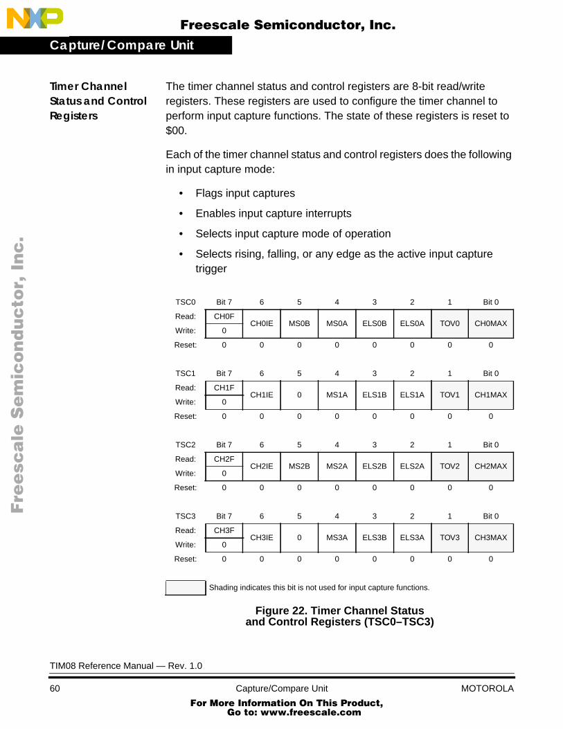
Capture/Compare Unit
F
ree
sca
le S
em
ico
nd
uc
tor,
I
Freescale Semiconductor, Inc.n
c..
.
Timer ChannelStatus and ControlRegisters
The timer channel status and control registers are 8-bit read/writeregisters. These registers are used to configure the timer channel toperform input capture functions. The state of these registers is reset to$00.
Each of the timer channel status and control registers does the followingin input capture mode:
• Flags input captures
• Enables input capture interrupts
• Selects input capture mode of operation
• Selects rising, falling, or any edge as the active input capturetrigger
Figure 22. Timer Channel Statusand Control Registers (TSC0–TSC3)
TSC0 Bit 7 6 5 4 3 2 1 Bit 0
Read: CH0FCH0IE MS0B MS0A ELS0B ELS0A TOV0 CH0MAX
Write: 0
Reset: 0 0 0 0 0 0 0 0
TSC1 Bit 7 6 5 4 3 2 1 Bit 0
Read: CH1FCH1IE 0 MS1A ELS1B ELS1A TOV1 CH1MAX
Write: 0
Reset: 0 0 0 0 0 0 0 0
TSC2 Bit 7 6 5 4 3 2 1 Bit 0
Read: CH2FCH2IE MS2B MS2A ELS2B ELS2A TOV2 CH2MAX
Write: 0
Reset: 0 0 0 0 0 0 0 0
TSC3 Bit 7 6 5 4 3 2 1 Bit 0
Read: CH3FCH3IE 0 MS3A ELS3B ELS3A TOV3 CH3MAX
Write: 0
Reset: 0 0 0 0 0 0 0 0
Shading indicates this bit is not used for input capture functions.
TIM08 Reference Manual — Rev. 1.0
60 Capture/Compare Unit MOTOROLA For More Information On This Product,
Go to: www.freescale.com

Capture/Compare UnitInput Capture (IC) Functions
F
ree
sca
le S
em
ico
nd
uc
tor,
I
Freescale Semiconductor, Inc.n
c..
.
CHxF — Channel x Flag
When channel x is an input capture channel, this clearable bit is setwhen an active edge occurs on the channel x pin.
When CPU interrupts are enabled (CHxE:DMAxS = 1:0), clear CHxFby reading the channel x status and control register with CHxF set andthen writing a 0 to CHxF. If another interrupt request occurs before theclearing sequence is complete, then writing 0 to CHxF has no effect.Therefore, an interrupt request cannot be lost due to inadvertentclearing of CHxF.
When DMA service requests are available and enabled(CHxE:DMAxS = 1:1), clear CHxF by reading or writing to the low byteof the channel register (TCHxL).
Writing a 1 to this bit has no effect. Reset clears the CHxF bit.1 = Input capture has occurred on channel x.0 = No input capture has occurred on channel x.
CHxIE — Channel x Interrupt Enable
This read/write bit enables channel x interrupts. In microcontrollerswith a DMA module, the DMAxS bit in the timer DMA select registerselects channel x CPU interrupts or DMA service requests. Resetclears the CHxIE bit.
1 = Channel x interrupts enabled0 = Channel x interrupts disabled
MSxB — Mode Select bit B
This bit should be cleared for input capture mode operation.MSxB exists only in the channel 0 and channel 2 status and controlregisters, TSC0 and TSC2.
This read/write bit selects buffered OC or buffered PWM operation.Setting MS0B disables the channel 1 status and control register, andreverts TCH1 to general-purpose I/O. Setting MS2B disables thechannel 3 status and control register, and reverts TCH3 togeneral-purpose I/O. Reset clears the MSxB bit.
1 = Buffered OC/PWM mode enabled0 = Buffered OC/PWM mode disabled
TIM08 Reference Manual — Rev. 1.0
MOTOROLA Capture/Compare Unit 61 For More Information On This Product,
Go to: www.freescale.com

Capture/Compare Unit
F
ree
sca
le S
em
ico
nd
uc
tor,
I
Freescale Semiconductor, Inc.n
c..
.
MSxA — Mode Select bit A
This bit should be cleared for input capture operation.
This read/write bit selects input capture mode or unbuffered OC/PWMmode. MS0A and MS1A are active only when MS0B = 0. MS2A andMS3A are active only when MS2B = 0. Reset clears the MSxA bit.
1 = Unbuffered OC/PWM operation0 = Input capture operation
NOTE: Stop and reset the TIM before changing a channel function. Beforewriting to the mode select bits (MSxB and MSxA), set the timer stop andtimer reset bits (TSTOP and TRST) in the TSC register.
ELSxB and ELSxA — Edge/Level Select bits
When channel x is an input capture channel, these read/write bitscontrol the active edge sensing logic on channel x.
When ELSxB and ELSxA are both clear, channel x is not connectedto the port, and pin TCHx is available as a general-purpose I/O pin.Table 2 shows the configuration selected by ELSxB and ELSxA ininput capture mode. Reset clears the ELSxB and ELSxA bits.
NOTE: Before enabling the channel register for input capture, make sure thatthe PTE/TCHx pin is stable for a minimum of two bus clocks.
TOVx — Toggle on Overflow
This bit is unused for input capture operation.
CHxMAX — PWM 100% duty cycle
This bit is unused for input capture operation.
Table 2. Input Capture Mode and Edge Selection
MSxB:MSxA
ELSxB:ELSxA Mode Configuration
00 00 Output presetTCHx pin under port control;
not used in IC mode
00 01 Input capture Capture on rising edge only
00 10 Input capture Capture on falling edge only
00 11 Input capture Capture on rising or falling edge
TIM08 Reference Manual — Rev. 1.0
62 Capture/Compare Unit MOTOROLA For More Information On This Product,
Go to: www.freescale.com

Capture/Compare UnitInput Capture (IC) Functions
F
ree
sca
le S
em
ico
nd
uc
tor,
I
Freescale Semiconductor, Inc.n
c..
.
Timer ChannelRegisters
These read/write registers are used as the 16-bit input capture registerlatches for input capture functions. These registers latch the value ofTCNT when a specified transition is detected on the corresponding inputcapture pin. The state of these registers is indeterminate after reset.
In input capture mode (MSxB:MSxA = 0:0), reading the high byte of thechannel register (TCHxH) inhibits input captures until the low byte(TCHxL) is read. This prevents another input capture from overwritingthe TCHxH:TCHxL registers before the previous value has been read.An overwrite of TCHxH:TCHxL will occur if another IC is received beforethe TCHxH is read. The LDHX instruction may be used to read theseregisters.
NOTE: Writing to the timer channel registers will overwrite any input capturedata.
If a timer channel register is not used for an input capture function, it canbe used as a storage location.
TIM08 Reference Manual — Rev. 1.0
MOTOROLA Capture/Compare Unit 63 For More Information On This Product,
Go to: www.freescale.com
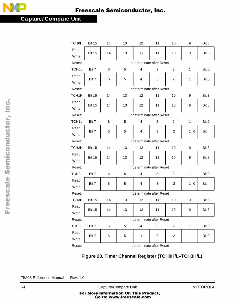
Capture/Compare Unit
F
ree
sca
le S
em
ico
nd
uc
tor,
I
Freescale Semiconductor, Inc.n
c..
.
Figure 23. Timer Channel Register (TCH0H/L–TCH3H/L)
TCH0H Bit 15 14 13 12 11 10 9 Bit 8
Read:Bit 15 14 13 12 11 10 9 Bit 8
Write:
Reset: Indeterminate after Reset
TCH0L Bit 7 6 5 4 3 2 1 Bit 0
Read:Bit 7 6 5 4 3 2 1 Bit 0
Write:
Reset: Indeterminate after Reset
TCH1H Bit 15 14 13 12 11 10 9 Bit 8
Read:Bit 15 14 13 12 11 10 9 Bit 8
Write:
Reset: Indeterminate after Reset
TCH1L Bit 7 6 5 4 3 2 1 Bit 0
Read:Bit 7 6 5 4 3 2 1 Bit 0
Write:
Reset: Indeterminate after Reset
TCH2H Bit 15 14 13 12 11 10 9 Bit 8
Read:Bit 15 14 13 12 11 10 9 Bit 8
Write:
Reset: Indeterminate after Reset
TCH2L Bit 7 6 5 4 3 2 1 Bit 0
Read:Bit 7 6 5 4 3 2 1 Bit 0
Write:
Reset: Indeterminate after Reset
TCH3H Bit 15 14 13 12 11 10 9 Bit 8
Read:Bit 15 14 13 12 11 10 9 Bit 8
Write:
Reset: Indeterminate after Reset
TCH3L Bit 7 6 5 4 3 2 1 Bit 0
Read:Bit 7 6 5 4 3 2 1 Bit 0
Write:
Reset: Indeterminate after Reset
TIM08 Reference Manual — Rev. 1.0
64 Capture/Compare Unit MOTOROLA For More Information On This Product,
Go to: www.freescale.com

Capture/Compare UnitUnbuffered Output Compare (OC) Functions
F
ree
sca
le S
em
ico
nd
uc
tor,
I
Freescale Semiconductor, Inc.n
c..
.
Unbuffered Output Compare (OC) Functions
Each of the TIM output compare pins TCH0–TCH3, when used as anunbuffered output compare function, has a dedicated 16-bit compareregister (TCHxH/L), a 16-bit comparator, and interrupt generation logic.The 16-bit modulo counter value, TCNT, is used as the timing referencefor all unbuffered output compares. When the programmed contents ofa timer channel register match TCNT, the 16-bit comparator generatesan output compare match, and certain automatic actions are initiated.These automatic actions can be a hardware interrupt request and statechanges at the related timer output pin.
See Unbuffered Output Compares for more information on the basicoperation of this function.
When the output compare match occurs, a status flag CHxF is set inTSCx. Figure 24 shows the timing of CHxF relative to the bus clocks, aswell as the timing relationships for state changes described in thefollowing paragraphs.
An output compare pin can be programmed to change states when anoutput compare match occurs. TSCx control bits ELSxA and ELSxBdetermine the output state of the pin on an output compare match. Anoutput compare channel can be programmed to toggle, clear, or set theTCHx pin on an output compare match. See Table 3 for the control bitconfigurations to select the state of an output compare pin.
If the interrupt enable bit (CHxIE) for this output compare function is setin TSCx, a CPU interrupt or DMA service request is generated on asuccessful output match. If the interrupt is disabled, CHxF can be polledby software to determine when an output compare match has occurred.See CPU Interrupts for details on interrupt operation and DMA ServiceRequests for details on service request operation.
TIM08 Reference Manual — Rev. 1.0
MOTOROLA Capture/Compare Unit 65 For More Information On This Product,
Go to: www.freescale.com
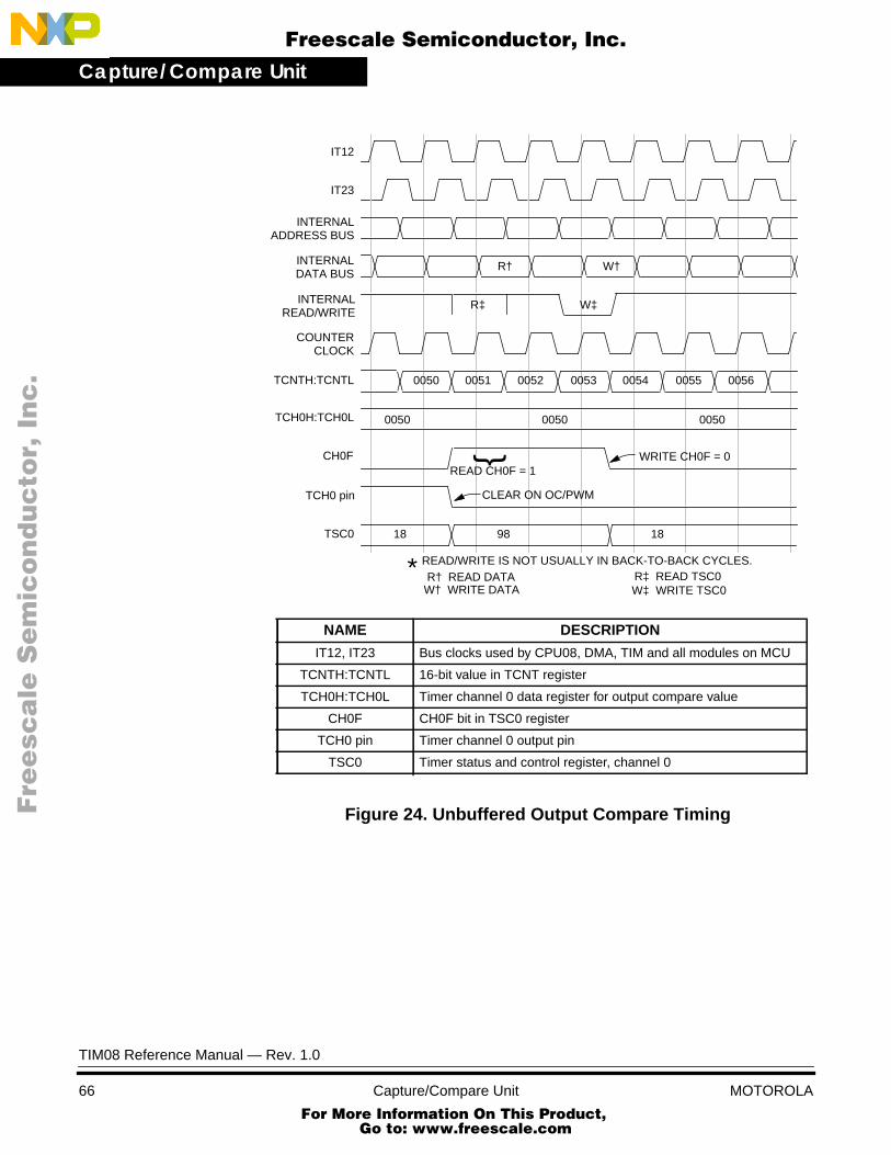
Capture/Compare Unit
F
ree
sca
le S
em
ico
nd
uc
tor,
I
Freescale Semiconductor, Inc.n
c..
.
Figure 24. Unbuffered Output Compare Timing
NAME DESCRIPTION
IT12, IT23 Bus clocks used by CPU08, DMA, TIM and all modules on MCU
TCNTH:TCNTL 16-bit value in TCNT register
TCH0H:TCH0L Timer channel 0 data register for output compare value
CH0F CH0F bit in TSC0 register
TCH0 pin Timer channel 0 output pin
TSC0 Timer status and control register, channel 0
IT23
IT12
INTERNAL
INTERNAL
COUNTER
TCNTH:TCNTL 0050 0051 0052 0053 0054 0055 0056
W‡
R†
R‡INTERNAL
TCH0H:TCH0L
CH0F
TCH0 pin CLEAR ON OC/PWM
READ/WRITE IS NOT USUALLY IN BACK-TO-BACK CYCLES.
0050 0050 0050
READ CH0F = 1WRITE CH0F = 0
W†
R†W† WRITE DATA
READ DATA
{
* R‡W‡
READ TSC0WRITE TSC0
TSC0 18 98 18
CLOCK
READ/WRITE
DATA BUS
ADDRESS BUS
TIM08 Reference Manual — Rev. 1.0
66 Capture/Compare Unit MOTOROLA For More Information On This Product,
Go to: www.freescale.com
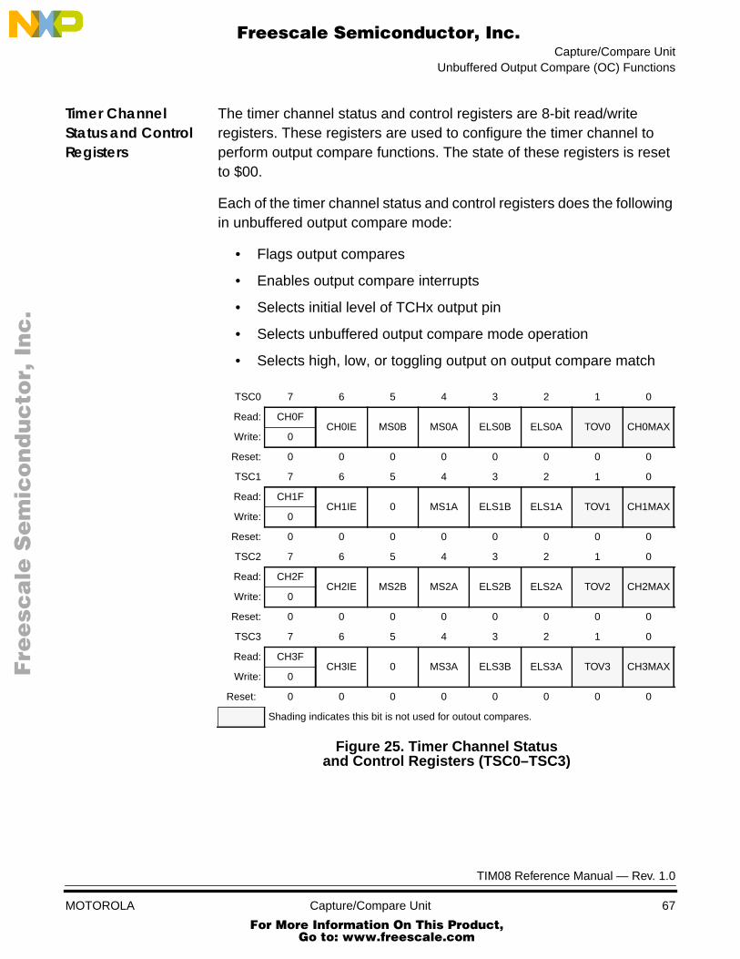
Capture/Compare UnitUnbuffered Output Compare (OC) Functions
F
ree
sca
le S
em
ico
nd
uc
tor,
I
Freescale Semiconductor, Inc.n
c..
.
Timer ChannelStatus and ControlRegisters
The timer channel status and control registers are 8-bit read/writeregisters. These registers are used to configure the timer channel toperform output compare functions. The state of these registers is resetto $00.
Each of the timer channel status and control registers does the followingin unbuffered output compare mode:
• Flags output compares
• Enables output compare interrupts
• Selects initial level of TCHx output pin
• Selects unbuffered output compare mode operation
• Selects high, low, or toggling output on output compare match
Figure 25. Timer Channel Statusand Control Registers (TSC0–TSC3)
TSC0 7 6 5 4 3 2 1 0
Read: CH0FCH0IE MS0B MS0A ELS0B ELS0A TOV0 CH0MAX
Write: 0
Reset: 0 0 0 0 0 0 0 0
TSC1 7 6 5 4 3 2 1 0
Read: CH1FCH1IE 0 MS1A ELS1B ELS1A TOV1 CH1MAX
Write: 0
Reset: 0 0 0 0 0 0 0 0
TSC2 7 6 5 4 3 2 1 0
Read: CH2FCH2IE MS2B MS2A ELS2B ELS2A TOV2 CH2MAX
Write: 0
Reset: 0 0 0 0 0 0 0 0
TSC3 7 6 5 4 3 2 1 0
Read: CH3FCH3IE 0 MS3A ELS3B ELS3A TOV3 CH3MAX
Write: 0
Reset: 0 0 0 0 0 0 0 0
Shading indicates this bit is not used for outout compares.
TIM08 Reference Manual — Rev. 1.0
MOTOROLA Capture/Compare Unit 67 For More Information On This Product,
Go to: www.freescale.com
Capture/Compare Unit
F
ree
sca
le S
em
ico
nd
uc
tor,
I
Freescale Semiconductor, Inc.n
c..
.
CHxF — Channel x Flag
When channel x is an output compare channel, CHxF is set when thevalue in the timer counter registers matches the value in the timerchannel x registers.
When CPU interrupts are enabled (CHxE:DMAxS = 1:0), clear CHxFby reading the channel x status and control register with CHxF set andthen writing a 0 to CHxF. If another interrupt request occurs before theclearing sequence is complete, writing 0 to CHxF has no effect.Therefore, an interrupt request cannot be lost due to inadvertentclearing of CHxF.
When DMA service requests are available and enabled(CHxE:DMAxS = 1:1), clear CHxF by reading or writing to the low byteof the channel register (TCHxL).
Writing a 1 to this bit has no effect. Reset clears the CHxF bit.1 = Output compare on channel x0 = No output compare on channel x
CHxIE — Channel x interrupt enable
This read/write bit enables channel x interrupts. In microcontrollerswith a DMA module, the DMAxS bit in the timer DMA select registerselects channel x CPU interrupts or DMA service requests. Resetclears the CHxIE bit.
1 = Channel x interrupts enabled0 = Channel x interrupts disabled
MSxB — Mode select bit B
This bit should be cleared for unbuffered output compareoperation. MSxB exists only in the channel 0 and channel 2 statusand control registers, TSC0 and TSC2.
This read/write bit selects buffered OC or buffered PWM operation.Setting MS0B disables the channel 1 status and control register, andreverts TCH1 to general-purpose I/O.
Setting MS2B disables the channel 3 status and control register, andreverts TCH3 to general-purpose I/O. Reset clears the MSxB bit.
1 = Buffered OC/PWM mode enabled0 = Buffered OC/PWM mode disabled
TIM08 Reference Manual — Rev. 1.0
68 Capture/Compare Unit MOTOROLA For More Information On This Product,
Go to: www.freescale.com
Capture/Compare UnitUnbuffered Output Compare (OC) Functions
F
ree
sca
le S
em
ico
nd
uc
tor,
I
Freescale Semiconductor, Inc.n
c..
.
MSxA — Mode Select bit A
This bit has different functions, depending on the state of ELSxB andELSxA.
When ELSxB:A = 00, this read/write bit selects the initial output levelof the TCHx pin. To select the level of your initial output, write theappropriate value to MSxA while ELSxB:A = 00. Then configure allbits in the TSCx as required for your application.
1 = Initial output level low0 = Initial output level high
When ELSxB:A ≠ 00, this read/write bit selects input capture mode orunbuffered OC/PWM mode. This bit should be set for unbufferedoutput compare operation. MS0A and MS1A are active only whenMS0B = 0. MS2A and MS3A are active only when MS2B = 0. Resetclears the MSxA bit.
1 = Unbuffered OC/PWM operation0 = Input capture operation
NOTE: Stop and reset the TIM before changing a channel function. Beforewriting to the mode select bits (MSxB and MSxA), set the timer stop andtimer reset bits (TSTOP and TRST) in the TSC register.
ELSxB and ELSxA — Edge/Level Select bits
When channel x is an output compare channel, ELSxB and ELSxAcontrol the channel x output behavior when an output compareoccurs.
When ELSxB and ELSxA are both clear, channel x is not connectedto the port, and pin TCHx is available as a general-purpose I/O pin.Table 3 shows the configuration selected by ELSxB and ELSxA inunbuffered output compare mode. Reset clears the ELSxB andELSxA bits.
TIM08 Reference Manual — Rev. 1.0
MOTOROLA Capture/Compare Unit 69 For More Information On This Product,
Go to: www.freescale.com
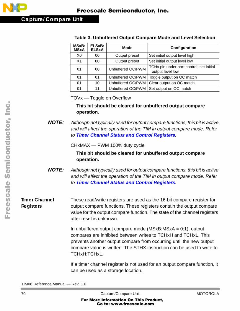
Capture/Compare Unit
F
ree
sca
le S
em
ico
nd
uc
tor,
I
Freescale Semiconductor, Inc.n
c..
.
TOVx — Toggle on OverflowThis bit should be cleared for unbuffered output compareoperation.
NOTE: Although not typically used for output compare functions, this bit is activeand will affect the operation of the TIM in output compare mode. Referto Timer Channel Status and Control Registers .
CHxMAX — PWM 100% duty cycle
This bit should be cleared for unbuffered output compareoperation.
NOTE: Although not typically used for output compare functions, this bit is activeand will affect the operation of the TIM in output compare mode. Referto Timer Channel Status and Control Registers .
Timer ChannelRegisters
These read/write registers are used as the 16-bit compare register foroutput compare functions. These registers contain the output comparevalue for the output compare function. The state of the channel registersafter reset is unknown.
In unbuffered output compare mode (MSxB:MSxA = 0:1), outputcompares are inhibited between writes to TCHxH and TCHxL. Thisprevents another output compare from occurring until the new outputcompare value is written. The STHX instruction can be used to write toTCHxH:TCHxL.
If a timer channel register is not used for an output compare function, itcan be used as a storage location.
Table 3. Unbuffered Output Compare Mode and Level Selection
MSxB:MSxA
ELSxB:ELSxA Mode Configuration
X0 00 Output preset Set initial output level high
X1 00 Output preset Set initial output level low
01 00 Unbuffered OC/PWMTCHx pin under port control; set initial
output level low.
01 01 Unbuffered OC/PWM Toggle output on OC match
01 10 Unbuffered OC/PWM Clear output on OC match
01 11 Unbuffered OC/PWM Set output on OC match
TIM08 Reference Manual — Rev. 1.0
70 Capture/Compare Unit MOTOROLA For More Information On This Product,
Go to: www.freescale.com

Capture/Compare UnitUnbuffered Output Compare (OC) Functions
F
ree
sca
le S
em
ico
nd
uc
tor,
I
Freescale Semiconductor, Inc.n
c..
.
Figure 26. Timer Channel Registers (TCH0H/L–TCH3H/L)
TCH0H Bit 15 14 13 12 11 10 9 Bit 8
Read:Bit 15 14 13 12 11 10 9 Bit 8
Write:
Reset: Indeterminate after Reset
TCH0L Bit 7 6 5 4 3 2 1 Bit 0
Read:Bit 7 6 5 4 3 2 1 Bit 0
Write:
Reset: Indeterminate after Reset
TCH1H Bit 15 14 13 12 11 10 9 Bit 8
Read:Bit 15 14 13 12 11 10 9 Bit 8
Write:
Reset: Indeterminate after Reset
TCH1L Bit 7 6 5 4 3 2 1 Bit 0
Read:Bit 7 6 5 4 3 2 1 Bit 0
Write:
Reset: Indeterminate after Reset
TCH2H Bit 15 14 13 12 11 10 9 Bit 8
Read:Bit 15 14 13 12 11 10 9 Bit 8
Write:
Reset: Indeterminate after Reset
TCH2L Bit 7 6 5 4 3 2 1 Bit 0
Read:Bit 7 6 5 4 3 2 1 Bit 0
Write:
Reset: Indeterminate after Reset
TCH3H Bit 15 14 13 12 11 10 9 Bit 8
Read:Bit 15 14 13 12 11 10 9 Bit 8
Write:
Reset: Indeterminate after Reset
TCH3L Bit 7 6 5 4 3 2 1 Bit 0
Read:Bit 7 6 5 4 3 2 1 Bit 0
Write:
Reset: Indeterminate after Reset
TIM08 Reference Manual — Rev. 1.0
MOTOROLA Capture/Compare Unit 71 For More Information On This Product,
Go to: www.freescale.com
Capture/Compare Unit
F
ree
sca
le S
em
ico
nd
uc
tor,
I
Freescale Semiconductor, Inc.n
c..
.
Buffered Output Compare (OC) Functions
TIM output compare pins TCH0 and TCH2 may be used as bufferedoutput compare functions. This is accomplished by linking twounbuffered output compare channels together to form one bufferedoutput compare channel. When used as buffered output compare pins,TCH0 and TCH2 have two dedicated 16-bit compare registers(TCHxH/L), two 16-bit comparators, and interrupt generation logic. The16-bit modulo counter value, TCNT, is used as the timing reference forall unbuffered PWM functions. When the programmed contents of theactive timer channel register matches TCNT, the active 16-bitcomparator generates an output compare match, and certain automaticactions are initiated for that output compare function. These automaticactions can be a hardware interrupt request and state changes at therelated timer output pin.
See Buffered Output Compares for information on the basic operationof this function.
When the output compare match occurs, a status flag CHxF is set inTSCx. Figure 27 shows the timing of CHxF relative to the bus clocks, aswell as the timing relationships for state changes described in thefollowing paragraphs.
An output compare pin can be programmed to change states when anoutput compare match occurs. TSCx control bits ELSxA and ELSxBdetermine the output state of the pin on an output compare match. Anoutput compare channel can be programmed to toggle, clear, or set theTCHx pin on an output compare match. See Table 4 for the control bitconfigurations to select the state of an output compare pin.
If the interrupt enable bit (CHxIE) for this output compare function is setin TSCx, a CPU interrupt is generated on a successful output match. Ifthe interrupt is disabled, CHxF can be polled by software to determinewhen an output compare match has occurred. See CPU Interrupts fordetails on interrupt operation.
NOTE: DMA service requests are not available in buffered output comparemode.
TIM08 Reference Manual — Rev. 1.0
72 Capture/Compare Unit MOTOROLA For More Information On This Product,
Go to: www.freescale.com

Capture/Compare UnitBuffered Output Compare (OC) Functions
F
ree
sca
le S
em
ico
nd
uc
tor,
I
Freescale Semiconductor, Inc.n
c..
.
To use TCH0 as a buffered output compare pin, set the MS0B bit inTSC0. This will disable TCH1 as a TIM pin, and it will revert to portcontrol. TSC0 controls and monitors the buffered output comparefunction, and TSC1 is unused. The channel 0 registers, TCH0H:TCH0L,initially control the output compare value on the TCH0 pin. Writing to thechannel 1 registers enables the channel 1 registers to synchronouslycontrol the output compare value at the beginning of the next counterperiod. At each subsequent overflow, the channel registers (0 or 1) lastwritten to control the output compare value. See Figure 27 .
To use TCH2 as a buffered output compare pin, set the MS2B bit inTSC2. This will disable TCH3 as a TIM pin, and it will revert to portcontrol. TSC2 controls and monitors the buffered output comparefunction, and TSC3 is unused. The channel 2 registers, TCH2H:TCH2L,initially control the output compare value on the TCH2 pin. Writing to thechannel 3 registers enables the channel 3 registers to synchronouslycontrol the output compare value at the beginning of the next PWMperiod. At each subsequent overflow, the channel registers (2 or 3) lastwritten to control the output compare value.
TIM08 Reference Manual — Rev. 1.0
MOTOROLA Capture/Compare Unit 73 For More Information On This Product,
Go to: www.freescale.com
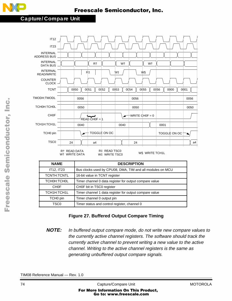
Capture/Compare Unit
F
ree
sca
le S
em
ico
nd
uc
tor,
I
Freescale Semiconductor, Inc.n
c..
.
Figure 27. Buffered Output Compare Timing
NOTE: In buffered output compare mode, do not write new compare values tothe currently active channel registers. The software should track thecurrently active channel to prevent writing a new value to the activechannel. Writing to the active channel registers is the same asgenerating unbuffered output compare signals.
IT23
IT12
INTERNAL
INTERNAL
COUNTER
TCNT 0050 0051 0052 0053 0054 0055 0056
W‡
R†
R‡INTERNAL
TCH0H:TCH0L
CH0F
TCH1H:TCH1L
TCH0 pin TOGGLE ON OC
0050 0050 0050
READ CH0F = 1WRITE CH0F = 0
0040 0040 0001
W†
R†W† WRITE DATA
READ DATA
{
R‡W‡
READ TSC0WRITE TSC0
0000 0001
TSC0 24 24 a4a4
NAME DESCRIPTION
IT12, IT23 Bus clocks used by CPU08, DMA, TIM and all modules on MCU
TCNTH:TCNTL 16-bit value in TCNT register
TCH0H:TCH0L Timer channel 0 data register for output compare value
CH0F CH0F bit in TSC0 register
TCH1H:TCH1L Timer channel 1 data register for output compare value
TCH0 pin Timer channel 0 output pin
TSC0 Timer status and control register, channel 0
W§
W§ WRITE TCH1L
W†
TOGGLE ON OC
CLOCK
READ/WRITE
DATA BUS
ADDRESS BUS
TMODH:TMODL 0056 0056 0056
TIM08 Reference Manual — Rev. 1.0
74 Capture/Compare Unit MOTOROLA For More Information On This Product,
Go to: www.freescale.com

Capture/Compare UnitTimer Channel Status and Control Registers
F
ree
sca
le S
em
ico
nd
uc
tor,
I
Freescale Semiconductor, Inc.n
c..
.
Timer Channel Status and Control Registers
The timer channel status and control registers are 8-bit read/writeregisters. These registers are used to configure the timer channel toperform output compare functions. The state of these registers is resetto $00.
Each of the timer channel status and control registers does the followingin buffered output compare mode:
• Flags output compares
• Enables output compare interrupts
• Selects initial level of TCHx output pin
• Selects buffered output compare mode of operation
• Selects high, low, or toggling output on output compare match
Figure 28. Timer Channel Status and ControlRegister (TSC0 and TSC2)
CHxF — Channel x flag
When channel x is a buffered output compare channel, CHxF is setwhen the value in the timer counter registers matches the value in thetimer channel x registers.
TSC0 Bit 7 6 5 4 3 2 1 Bit 0
Read: CH0FCH0IE MS0B MS0A ELS0B ELS0A TOV0 CH0MAX
Write: 0
Reset: 0 0 0 0 0 0 0 0
TSC2 Bit 7 6 5 4 3 2 1 Bit 0
Read: CH2FCH2IE MS2B MS2A ELS2B ELS2A TOV2 CH2MAX
Write: 0
Reset: 0 0 0 0 0 0 0 0
Shading indicates this bit is not used for output compares.
TIM08 Reference Manual — Rev. 1.0
MOTOROLA Capture/Compare Unit 75 For More Information On This Product,
Go to: www.freescale.com
Capture/Compare Unit
F
ree
sca
le S
em
ico
nd
uc
tor,
I
Freescale Semiconductor, Inc.n
c..
.
When CPU interrupts are enabled (CHxE:DMAxS = 1:0), clear CHxFby reading the channel x status and control register with CHxF set andwriting a 0 to CHxF. If another interrupt request occurs before theclearing sequence is complete, then writing 0 to CHxF has no effect.Therefore, an interrupt request cannot be lost due to inadvertentclearing of CHxF.
DMA service requests may not be used with buffered output comparefunctions.
Writing a 1 to this bit has no effect. Reset clears the CHxF bit.1 = Output compare on channel x0 = No output compare on channel x
CHxIE — Channel x interrupt enable
This read/write bit enables channel x interrupts. In microcontrollerswith a DMA module, the DMAxS bit in the timer DMA selectregister should be cleared to select channel x CPU interrupts.DMA service requests cannot be used with buffered OC mode. Resetclears the CHxIE bit.
1 = Channel x interrupts enabled0 = Channel x interrupts disabled
MSxB — Mode select bit B
This bit should be set for buffered OC operation. MSxB exists onlyin the channel 0 and channel 2 status and control registers, TSC0 andTSC2.
This read/write bit selects buffered OC or buffered PWM operation.Setting MS0B disables the channel 1 status and control register, andreverts TCH1 to general-purpose I/O. Setting MS2B disables thechannel 3 status and control register, and reverts TCH3 togeneral-purpose I/O. Reset clears the MSxB bit.
1 = Buffered OC/PWM mode enabled0 = Buffered OC/PWM mode disabled
MSxA — Mode select bit A
This bit has different functions, depending on the state of ELSxB andELSxA.
TIM08 Reference Manual — Rev. 1.0
76 Capture/Compare Unit MOTOROLA For More Information On This Product,
Go to: www.freescale.com
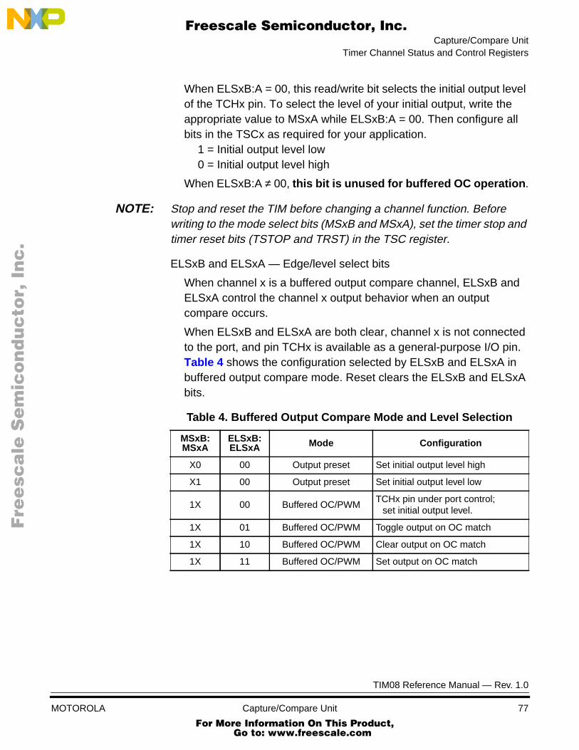
Capture/Compare UnitTimer Channel Status and Control Registers
F
ree
sca
le S
em
ico
nd
uc
tor,
I
Freescale Semiconductor, Inc.n
c..
.
When ELSxB:A = 00, this read/write bit selects the initial output levelof the TCHx pin. To select the level of your initial output, write theappropriate value to MSxA while ELSxB:A = 00. Then configure allbits in the TSCx as required for your application.
1 = Initial output level low0 = Initial output level high
When ELSxB:A ≠ 00, this bit is unused for buffered OC operation .
NOTE: Stop and reset the TIM before changing a channel function. Beforewriting to the mode select bits (MSxB and MSxA), set the timer stop andtimer reset bits (TSTOP and TRST) in the TSC register.
ELSxB and ELSxA — Edge/level select bits
When channel x is a buffered output compare channel, ELSxB andELSxA control the channel x output behavior when an outputcompare occurs.
When ELSxB and ELSxA are both clear, channel x is not connectedto the port, and pin TCHx is available as a general-purpose I/O pin.Table 4 shows the configuration selected by ELSxB and ELSxA inbuffered output compare mode. Reset clears the ELSxB and ELSxAbits.
Table 4. Buffered Output Compare Mode and Level Selection
MSxB:MSxA
ELSxB:ELSxA Mode Configuration
X0 00 Output preset Set initial output level high
X1 00 Output preset Set initial output level low
1X 00 Buffered OC/PWMTCHx pin under port control;
set initial output level.
1X 01 Buffered OC/PWM Toggle output on OC match
1X 10 Buffered OC/PWM Clear output on OC match
1X 11 Buffered OC/PWM Set output on OC match
TIM08 Reference Manual — Rev. 1.0
MOTOROLA Capture/Compare Unit 77 For More Information On This Product,
Go to: www.freescale.com
Capture/Compare Unit
F
ree
sca
le S
em
ico
nd
uc
tor,
I
Freescale Semiconductor, Inc.n
c..
.
TOVx — Toggle on overflow
This bit should be cleared for buffered output compareoperation.
NOTE: Although not typically used for output compare functions, this bit is activeand will affect the operation of the TIM in output compare mode. SeeTimer Channel Status and Control Registers .
CHxMAX — PWM 100% duty cycle
This bit should be cleared for buffered output compareoperation.
NOTE: Although not typically used for output compare functions, this bit is activeand will affect the operation of the TIM in output compare mode. SeeTimer Channel Status and Control Registers .
Timer ChannelRegisters
These read/write registers are used as the 16-bit compare register foroutput compare functions. These registers contain the output comparevalue for the output compare function. The state of the channel registersafter reset is unknown.
In buffered output compare mode (MSxB = 1), output compares areinhibited between writes to TCHxH and TCHxL of the active channel.This prevents another output compare from occurring until the newoutput compare value is written. Output compares are allowed betweenwrites to TCHxH and TCHxL of the inactive channel. The STHXinstruction can be used to write to TCHxH:L.
If a timer channel register is not used for an output compare function, itcan be used as a storage location.
TIM08 Reference Manual — Rev. 1.0
78 Capture/Compare Unit MOTOROLA For More Information On This Product,
Go to: www.freescale.com

Capture/Compare UnitTimer Channel Status and Control Registers
F
ree
sca
le S
em
ico
nd
uc
tor,
I
Freescale Semiconductor, Inc.n
c..
.
Figure 29. Timer Channel Registers (TCH0H/L–TCH3H/L)
TCH0H Bit 15 14 13 12 11 10 9 Bit 8
Read:Bit 15 14 13 12 11 10 9 Bit 8
Write:
Reset: Indeterminate after Reset
TCH0L Bit 7 6 5 4 3 2 1 Bit 0
Read:Bit 7 6 5 4 3 2 1 Bit 0
Write:
Reset: Indeterminate after Reset
TCH1H Bit 15 14 13 12 11 10 9 Bit 8
Read:Bit 15 14 13 12 11 10 9 Bit 8
Write:
Reset: Indeterminate after Reset
TCH1L Bit 7 6 5 4 3 2 1 Bit 0
Read:Bit 7 6 5 4 3 2 1 Bit 0
Write:
Reset: Indeterminate after Reset
TCH2H Bit 15 14 13 12 11 10 9 Bit 8
Read:Bit 15 14 13 12 11 10 9 Bit 8
Write:
Reset: Indeterminate after Reset
TCH2L Bit 7 6 5 4 3 2 1 Bit 0
Read:Bit 7 6 5 4 3 2 1 Bit 0
Write:
Reset: Indeterminate after Reset
TCH3H Bit 15 14 13 12 11 10 9 Bit 8
Read:Bit 15 14 13 12 11 10 9 Bit 8
Write:
Reset: Indeterminate after Reset
TCH3L Bit 7 6 5 4 3 2 1 Bit 0
Read:Bit 7 6 5 4 3 2 1 Bit 0
Write:
Reset: Indeterminate after Reset
TIM08 Reference Manual — Rev. 1.0
MOTOROLA Capture/Compare Unit 79 For More Information On This Product,
Go to: www.freescale.com
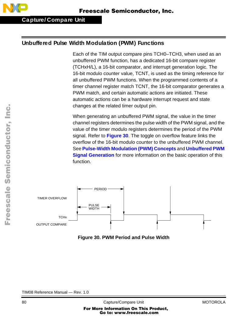
Capture/Compare Unit
F
ree
sca
le S
em
ico
nd
uc
tor,
I
Freescale Semiconductor, Inc.n
c..
.
Unbuffered Pulse Width Modulation (PWM) Functions
Each of the TIM output compare pins TCH0–TCH3, when used as anunbuffered PWM function, has a dedicated 16-bit compare register(TCHxH/L), a 16-bit comparator, and interrupt generation logic. The16-bit modulo counter value, TCNT, is used as the timing reference forall unbuffered PWM functions. When the programmed contents of atimer channel register match TCNT, the 16-bit comparator generates aPWM match, and certain automatic actions are initiated. Theseautomatic actions can be a hardware interrupt request and statechanges at the related timer output pin.
When generating an unbuffered PWM signal, the value in the timerchannel registers determines the pulse width of the PWM signal, and thevalue of the timer modulo registers determines the period of the PWMsignal. Refer to Figure 30 . The toggle on overflow feature links theoverflow of the 16-bit modulo counter to the unbuffered PWM channel.See Pulse-Width Modulation (PWM) Concepts and Unbuffered PWMSignal Generation for more information on the basic operation of thisfunction.
Figure 30. PWM Period and Pulse Width
OUTPUT COMPARE
TIMER OVERFLOW
TCHx
PERIOD
PULSEWIDTH
TIM08 Reference Manual — Rev. 1.0
80 Capture/Compare Unit MOTOROLA For More Information On This Product,
Go to: www.freescale.com
Capture/Compare UnitUnbuffered Pulse Width Modulation (PWM) Functions
F
ree
sca
le S
em
ico
nd
uc
tor,
I
Freescale Semiconductor, Inc.n
c..
.
When the PWM match occurs, a status flag CHxF is set in TSCx. Figure31 shows the timing of CHxF relative to the bus clocks, as well as thetiming relationships for state changes and interrupts described in thefollowing paragraphs.
A PWM pin can be programmed to change states when a PWM matchoccurs, thereby determining the pulse width of the PWM signal. TSCxcontrol bits ELSxA and ELSxB determine the output state of the pin ona PWM match. An unbuffered PWM channel can be programmed totoggle, clear, or set the TCHx pin on a PWM match. Table 5 for thecontrol bit configurations to select the state of a PWM signal pin.
If the interrupt enable bit (CHxIE) for this PWM function is set in TSCx,a CPU interrupt or DMA service request is generated on a PWM match.If the interrupt is disabled, CHxF can be polled by software to determinewhen a match has occurred. See CPU Interrupts for details on interruptoperation and See DMA Service Requests for details on servicerequest operation.
To generate a signal with 100% duty cycle, use the CHxMAX bit in theTSCx. To generate a signal with 0% duty cycle, program the PWMchannel to either set or clear (not toggle) on PWM match, then clear theTOVx bit to start a 0% duty cycle signal.
NOTE: In PWM signal generation, do not program the PWM channel to toggleon PWM match. Toggling on PWM match prevents reliable 0% dutycycle generation and removes the ability of the channel to self-correct inthe event of software error or noise. Toggling on PWM match can alsocause incorrect PWM signal generation when changing the PWM pulsewidth to a new, much larger value.
TIM08 Reference Manual — Rev. 1.0
MOTOROLA Capture/Compare Unit 81 For More Information On This Product,
Go to: www.freescale.com
Capture/Compare Unit
F
ree
sca
le S
em
ico
nd
uc
tor,
I
Freescale Semiconductor, Inc.n
c..
.
Figure 31. Unbuffered PWM Timing
NAME DESCRIPTIONIT12, IT23 Bus clocks used by CPU08, DMA, TIM and all modules on MCU
TCNTH:TCNTL 16-bit value in TCNT registerTCH0H:TCH0L Timer channel 0 data register for output compare value
CH0F CH0F bit in TSC0 registerTMODH:TMODL Timer counter modulo register
TOF Timer counter overflow flag (TOF) bit in TSC registerTCH0 pin Timer channel 0 output pin
TSC0 Timer status and control register, channel 0TSC Timer status and control register
READ/WRITE IS NOT USUALLY IN BACK-TO-BACK CYCLES.R†
W† WRITE DATAREAD DATA
*R‡W‡
READ TSC0WRITE TSC0
IT23
IT12
INTERNAL
INTERNAL
COUNTER
TCNTH:TCNTL 0050 0051 0052 0053 0054 0055 0000
W‡
R†
R‡INTERNAL
TCH0H:TCH0L
CH0F
TCH0 PIN CLEAR ON PWM MATCH
0050 0050 0050
READ CH0F = 1WRITE CH0F = 0
W†
{0001
TMODH:TMODL
TOF
0055 0055 0055
TSC0 1A 9A 1A
TOGGLE ON OVERFLOW
TSC 00 80
ADDRESS BUS
DATA BUS
READ/WRITE
CLOCK
TIM08 Reference Manual — Rev. 1.0
82 Capture/Compare Unit MOTOROLA For More Information On This Product,
Go to: www.freescale.com

Capture/Compare UnitUnbuffered Pulse Width Modulation (PWM) Functions
F
ree
sca
le S
em
ico
nd
uc
tor,
I
Freescale Semiconductor, Inc.n
c..
.
Timer ChannelStatus and ControlRegisters
The timer channel status and control registers are 8-bit read/writeregisters. These registers are used to configure the timer channel toperform PWM functions. The state of these registers is reset to $00.
Each of the timer channel status and control registers does the followingin unbuffered PWM mode:
• Flags pulse width matches
• Enables PWM interrupts
• Selects initial level of TCHx output pin
• Selects unbuffered PWM operation
• Selects high, low, or toggling output on PWM match
• Selects output toggling on timer overflow
• Selects 100% PWM duty cycle
TIM08 Reference Manual — Rev. 1.0
MOTOROLA Capture/Compare Unit 83 For More Information On This Product,
Go to: www.freescale.com
Capture/Compare Unit
F
ree
sca
le S
em
ico
nd
uc
tor,
I
Freescale Semiconductor, Inc.n
c..
.
Figure 32. Timer Channel Status and Control Registers(TSC0–TSC3)
CHxF — Channel x flag
When channel x is a PWM channel, CHxF is set when the value in thetimer counter registers matches the value in the timer channel xregisters.
When CPU interrupts are enabled (CHxE:DMAxS = 1:0), clear CHxFby reading the channel x status and control register with CHxF set andthen writing a 0 to CHxF. If another interrupt request occurs before theclearing sequence is complete, then writing 0 to CHxF has no effect.Therefore, an interrupt request cannot be lost due to inadvertentclearing of CHxF.
TSC0 Bit 7 6 5 4 3 2 1 Bit 0
Read: CH0FCH0IE MS0B MS0A ELS0B ELS0A TOV0 CH0MAX
Write: 0
Reset: 0 0 0 0 0 0 0 0
TSC1 Bit 7 6 5 4 3 2 1 0
Read: CH1FCH1IE 0 MS1A ELS1B ELS1A TOV1 CH1MAX
Write: 0
Reset: 0 0 0 0 0 0 0 0
TSC2 Bit 7 6 5 4 3 2 1 0
Read: CH2FCH2IE MS2B MS2A ELS2B ELS2A TOV2 CH2MAX
Write: 0
Reset: 0 0 0 0 0 0 0 0
TSC3 Bit 7 6 5 4 3 2 1 Bit 0
Read: CH3FCH3IE 0 MS3A ELS3B ELS3A TOV3 CH3MAX
Write: 0
Reset: 0 0 0 0 0 0 0 0
TIM08 Reference Manual — Rev. 1.0
84 Capture/Compare Unit MOTOROLA For More Information On This Product,
Go to: www.freescale.com

Capture/Compare UnitUnbuffered Pulse Width Modulation (PWM) Functions
F
ree
sca
le S
em
ico
nd
uc
tor,
I
Freescale Semiconductor, Inc.n
c..
.
When DMA service requests are available and enabled(CHxE:DMAxS = 1:1), clear CHxF by reading or writing to the low byteof the channel register (TCHxL).
Writing a 1 to this bit has no effect. Reset clears the CHxF bit.1 = PWM match on channel x0 = No PWM match on channel x
CHxIE — Channel x interrupt enable
This read/write bit enables channel x interrupts. In microcontrollerswith a DMA module, the DMAxS bit in the timer DMA select registerselects channel x CPU interrupts or DMA service requests. Resetclears the CHxIE bit.
1 = Channel x interrupts enabled0 = Channel x interrupts disabled
MSxB — Mode select bit B
This bit should be cleared for unbuffered PWM operation. MSxBexists only in the channel 0 and channel 2 status and control registers,TSC0 and TSC2.
This read/write bit selects buffered OC or buffered PWM operation.Setting MS0B disables the channel 1 status and control register andreverts TCH1 to general-purpose I/O. Setting MS2B disables thechannel 3 status and control register and reverts TCH3 togeneral-purpose I/O. Reset clears the MSxB bit.
1 = Buffered OC/PWM mode enabled0 = Buffered OC/PWM mode disabled
MSxA — Mode select bit A
This bit has different functions, depending on the state of ELSxB andELSxA.
When ELSxB:A = 00, this read/write bit selects the initial output levelof the TCHx pin. To select the level of your initial output, write theappropriate value to MSxA while ELSxB:A = 00. Then configure allbits in the TSCx as required for your application.
1 = Initial output level low0 = Initial output level high
TIM08 Reference Manual — Rev. 1.0
MOTOROLA Capture/Compare Unit 85 For More Information On This Product,
Go to: www.freescale.com
Capture/Compare Unit
F
ree
sca
le S
em
ico
nd
uc
tor,
I
Freescale Semiconductor, Inc.n
c..
.
When ELSxB:A ≠ 00, this read/write bit selects input capture mode orunbuffered OC/PWM mode. This bit should be set for unbufferedPWM operation. MS0A and MS1A are active only when MS0B = 0.MS2A and MS3A are active only when MS2B = 0. Reset clears theMSxA bit.
1 = Unbuffered OC/PWM operation0 = Input capture operation
NOTE: Stop and reset the TIM before changing a channel function. Beforewriting to the mode select bits (MSxB and MSxA), set the timer stop andtimer reset bits (TSTOP and TRST) in the TSC register.
ELSxB and ELSxA — Edge/level select bits
When channel x is a PWM channel, ELSxB and ELSxA control thechannel x output behavior when a pulse width match occurs.
When ELSxB and ELSxA are both clear, channel x is not connectedto the port, and pin TCHx is available as a general-purpose I/O pin.Table 5 shows the configuration selected by ELSxB and ELSxA inunbuffered PWM mode. Reset clears the ELSxB and ELSxA bits.
Table 5. Unbuffered PWM Mode and Level Selection
MSxB:MSxA
ELSxB:ELSxA Mode Configuration
X0 00 Output preset Set initial output level high
X1 00 Output preset Set initial output level low
01 00 Unbuffered OC/PWMTCHx pin under port control;
set initial output level low.
01 01 Unbuffered OC/PWM Toggle output on PWM match
01 10 Unbuffered OC/PWM Clear output on PWM match
01 11 Unbuffered OC/PWM Set output on PWM match
TIM08 Reference Manual — Rev. 1.0
86 Capture/Compare Unit MOTOROLA For More Information On This Product,
Go to: www.freescale.com
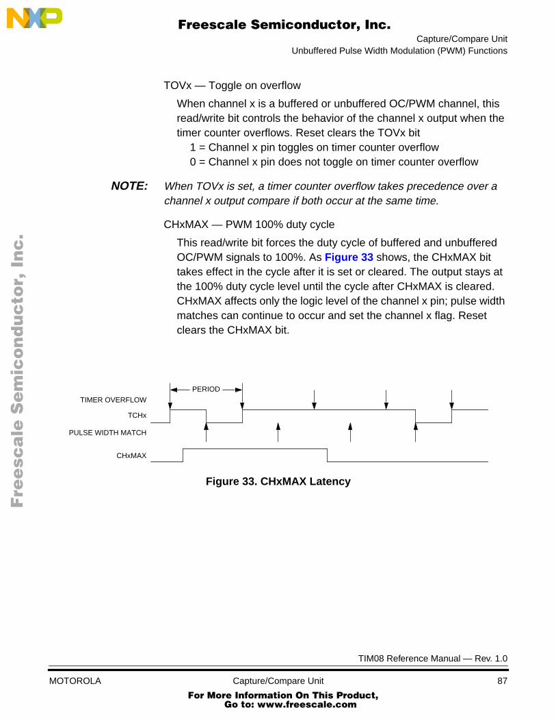
Capture/Compare UnitUnbuffered Pulse Width Modulation (PWM) Functions
F
ree
sca
le S
em
ico
nd
uc
tor,
I
Freescale Semiconductor, Inc.n
c..
.
TOVx — Toggle on overflow
When channel x is a buffered or unbuffered OC/PWM channel, thisread/write bit controls the behavior of the channel x output when thetimer counter overflows. Reset clears the TOVx bit
1 = Channel x pin toggles on timer counter overflow0 = Channel x pin does not toggle on timer counter overflow
NOTE: When TOVx is set, a timer counter overflow takes precedence over achannel x output compare if both occur at the same time.
CHxMAX — PWM 100% duty cycle
This read/write bit forces the duty cycle of buffered and unbufferedOC/PWM signals to 100%. As Figure 33 shows, the CHxMAX bittakes effect in the cycle after it is set or cleared. The output stays atthe 100% duty cycle level until the cycle after CHxMAX is cleared.CHxMAX affects only the logic level of the channel x pin; pulse widthmatches can continue to occur and set the channel x flag. Resetclears the CHxMAX bit.
Figure 33. CHxMAX Latency
PULSE WIDTH MATCH
TIMER OVERFLOW
TCHx
PERIOD
CHxMAX
TIM08 Reference Manual — Rev. 1.0
MOTOROLA Capture/Compare Unit 87 For More Information On This Product,
Go to: www.freescale.com
Capture/Compare Unit
F
ree
sca
le S
em
ico
nd
uc
tor,
I
Freescale Semiconductor, Inc.n
c..
.
Timer ChannelRegisters
These read/write registers are used as the 16-bit compare register forPWM functions. These registers contain the pulse width match value forthe PWM function. The state of the channel registers after reset isunknown.
In unbuffered PWM mode (MSxB:MSxA = 0:1), pulse width matches areinhibited between writes to TCHxH and TCHxL. This prevents anothermatch from occurring until the new pulse width value is written. TheSTHX instruction can be used to write to TCHxH:L.
If a timer channel register is not used for a PWM function, it can be usedas a storage location.
TIM08 Reference Manual — Rev. 1.0
88 Capture/Compare Unit MOTOROLA For More Information On This Product,
Go to: www.freescale.com

Capture/Compare UnitUnbuffered Pulse Width Modulation (PWM) Functions
F
ree
sca
le S
em
ico
nd
uc
tor,
I
Freescale Semiconductor, Inc.n
c..
.
Figure 34. Timer Channel Registers (TCH0H/L–TCH3H/L)
TCH0H Bit 15 14 13 12 11 10 9 Bit 8
Read:Bit 15 14 13 12 11 10 9 Bit 8
Write:
Reset: Indeterminate after Reset
TCH0L Bit 7 6 5 4 3 2 1 Bit 0
Read:Bit 7 6 5 4 3 2 1 Bit 0
Write:
Reset: Indeterminate after Reset
TCH1H Bit 15 14 13 12 11 10 9 Bit 8
Read:Bit 15 14 13 12 11 10 9 Bit 8
Write:
Reset: Indeterminate after Reset
TCH1L Bit 7 6 5 4 3 2 1 Bit 0
Read:Bit 7 6 5 4 3 2 1 Bit 0
Write:
Reset: Indeterminate after Reset
TCH2H Bit 15 14 13 12 11 10 9 Bit 8
Read:Bit 15 14 13 12 11 10 9 Bit 8
Write:
Reset: Indeterminate after Reset
TCH2L Bit 7 6 5 4 3 2 1 Bit 0
Read:Bit 7 6 5 4 3 2 1 Bit 0
Write:
Reset: Indeterminate after Reset
TCH3H Bit 15 14 13 12 11 10 9 Bit 8
Read:Bit 15 14 13 12 11 10 9 Bit 8
Write:
Reset: Indeterminate after Reset
TCH3L Bit 7 6 5 4 3 2 1 Bit 0
Read:Bit 7 6 5 4 3 2 1 Bit 0
Write:
Reset: Indeterminate after Reset
TIM08 Reference Manual — Rev. 1.0
MOTOROLA Capture/Compare Unit 89 For More Information On This Product,
Go to: www.freescale.com
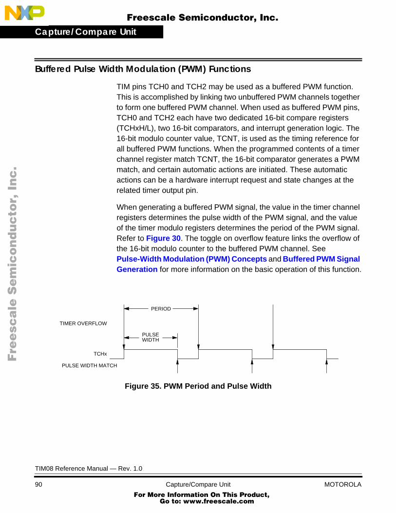
Capture/Compare Unit
F
ree
sca
le S
em
ico
nd
uc
tor,
I
Freescale Semiconductor, Inc.n
c..
.
Buffered Pulse Width Modulation (PWM) Functions
TIM pins TCH0 and TCH2 may be used as a buffered PWM function.This is accomplished by linking two unbuffered PWM channels togetherto form one buffered PWM channel. When used as buffered PWM pins,TCH0 and TCH2 each have two dedicated 16-bit compare registers(TCHxH/L), two 16-bit comparators, and interrupt generation logic. The16-bit modulo counter value, TCNT, is used as the timing reference forall buffered PWM functions. When the programmed contents of a timerchannel register match TCNT, the 16-bit comparator generates a PWMmatch, and certain automatic actions are initiated. These automaticactions can be a hardware interrupt request and state changes at therelated timer output pin.
When generating a buffered PWM signal, the value in the timer channelregisters determines the pulse width of the PWM signal, and the valueof the timer modulo registers determines the period of the PWM signal.Refer to Figure 30 . The toggle on overflow feature links the overflow ofthe 16-bit modulo counter to the buffered PWM channel. SeePulse-Width Modulation (PWM) Concepts and Buffered PWM SignalGeneration for more information on the basic operation of this function.
Figure 35. PWM Period and Pulse Width
PULSE WIDTH MATCH
TIMER OVERFLOW
TCHx
PERIOD
PULSEWIDTH
TIM08 Reference Manual — Rev. 1.0
90 Capture/Compare Unit MOTOROLA For More Information On This Product,
Go to: www.freescale.com

Capture/Compare UnitBuffered Pulse Width Modulation (PWM) Functions
F
ree
sca
le S
em
ico
nd
uc
tor,
I
Freescale Semiconductor, Inc.n
c..
.
When the PWM match occurs, a status flag CHxF is set in TSCx. Figure36, in the previous section, shows the timing of CHxF relative to the busclocks, as well as the timing relationships for state changes andinterrupts described in the following paragraphs.
A PWM pin can be programmed to change states when a PWM matchoccurs, thereby determining the pulse width of the PWM signal. TSCxcontrol bits ELSxA and ELSxB determine the output state of the pin ona PWM match. An unbuffered PWM channel can be programmed totoggle, clear, or set the TCHx pin on a PWM match. Table 6 for thecontrol bit configurations to select the state of a PWM signal pin.
If the interrupt enable bit (CHxIE) for this PWM function is set in TSCx,a CPU interrupt is generated on a PWM match. If the interrupt isdisabled, CHxF can be polled by software to determine when a matchhas occurred. See CPU Interrupts for details on interrupt operation.
NOTE: DMA service requests are not available in buffered PWM mode.
To generate a signal with 100% duty cycle, use the CHxMAX bit in theTSCx. To generate a signal with 0% duty cycle, program the PWMchannel to either set or clear (not toggle) on PWM match, then clear theTOVx bit to start a 0% duty cycle signal.
NOTE: In PWM signal generation, do not program the PWM channel to toggleon PWM match. Toggling on PWM match prevents reliable 0% dutycycle generation and removes the ability of the channel to self-correct inthe event of software error or noise. Toggling on PWM match can alsocause incorrect PWM signal generation when changing the PWM pulsewidth to a new, much larger value.
To use TCH0 as a buffered PWM pin, set the MS0B bit in TSC0. This willdisable TCH1 as a TIM pin, and it will revert to port control. TSC0controls and monitors the buffered PWM function, and TSC1 is unused.The channel 0 registers, TCH0H:TCH0L, initially control the pulse widthon the TCH0 pin. Writing to the channel 1 registers enables the channel1 registers to synchronously control the pulse width at the beginning ofthe next PWM period. At each subsequent overflow, the channelregisters (0 or 1) last written to control the pulse width. Figure 36 .
TIM08 Reference Manual — Rev. 1.0
MOTOROLA Capture/Compare Unit 91 For More Information On This Product,
Go to: www.freescale.com
Capture/Compare Unit
F
ree
sca
le S
em
ico
nd
uc
tor,
I
Freescale Semiconductor, Inc.n
c..
.
To use TCH2 as a buffered PWM pin, set the MS2B bit in TSC2. This willdisable TCH3 as a TIM pin, and it will revert to port control. TSC2controls and monitors the buffered PWM function, and TSC3 is unused.The channel 2 registers, TCH2H:TCH2L, initially control the pulse widthon the TCH2 pin. Writing to the channel 3 registers enables the channel3 registers to synchronously control the pulse width at the beginning ofthe next PWM period. At each subsequent overflow, the channelregisters (2 or 3) last written to control the pulse width.
NOTE: In buffered PWM signal generation, do not write new pulse width valuesto the currently active channel registers. The software should track thecurrently active channel to prevent writing a new value to the activechannel. Writing to the active channel registers is the same asgenerating unbuffered PWM signals.
TIM08 Reference Manual — Rev. 1.0
92 Capture/Compare Unit MOTOROLA For More Information On This Product,
Go to: www.freescale.com

Capture/Compare UnitBuffered Pulse Width Modulation (PWM) Functions
F
ree
sca
le S
em
ico
nd
uc
tor,
I
Freescale Semiconductor, Inc.n
c..
.
Figure 36. Buffered PWM Timing
NAME DESCRIPTIONIT12, IT23 Bus clocks used by CPU08, DMA, TIM and all modules on MCU
TCNTH:TCNTL 16-bit value in TCNT register
TCH0H:TCHOL Timer channel 0 data register for output compare value
CH0F CH0F bit in TSC0 register
TMODH:TMODL Timer counter modulo register
TOF Timer counter overflow flag (TOF) bit in TSC register
TCH0 pin Timer channel 0 output pin
TSC0 Timer status and control register, channel 0
TSC Timer status and control register
IT23
IT12
INTERNAL
INTERNAL
COUNTER
TCNT 0050 0051 0052 0053 0054 0055 0056
W‡
R†
R‡INTERNAL
TCH0H:TCH0L
CH0F
TCH1H:TCH1L
TCH0 PIN CLEAR ON PWM MATCH
0050 0050 0050 0050
READ CH0F = 1WRITE CH0F = 0
0040 0040 0001
W†
R†W† WRITE DATA
READ DATA
{
R‡W‡
READ TSC0WRITE TSC0
0000 00020001
W*
W†
W* WRITE TCH1L
TSC0 24 24 a4a4
TOGGLE ON OVERFLOW
TMODH:TMODL
TOF
0056 0056 0056 0056
TSC 00 80
ADDRESS BUS
DATA BUS
READ/WRITE
CLOCK
TIM08 Reference Manual — Rev. 1.0
MOTOROLA Capture/Compare Unit 93 For More Information On This Product,
Go to: www.freescale.com
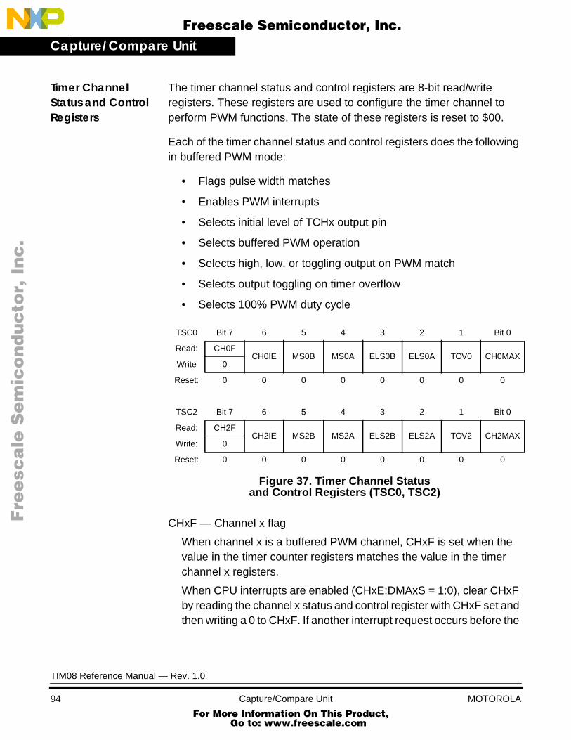
Capture/Compare Unit
F
ree
sca
le S
em
ico
nd
uc
tor,
I
Freescale Semiconductor, Inc.n
c..
.
Timer ChannelStatus and ControlRegisters
The timer channel status and control registers are 8-bit read/writeregisters. These registers are used to configure the timer channel toperform PWM functions. The state of these registers is reset to $00.
Each of the timer channel status and control registers does the followingin buffered PWM mode:
• Flags pulse width matches
• Enables PWM interrupts
• Selects initial level of TCHx output pin
• Selects buffered PWM operation
• Selects high, low, or toggling output on PWM match
• Selects output toggling on timer overflow
• Selects 100% PWM duty cycle
Figure 37. Timer Channel Statusand Control Registers (TSC0, TSC2)
CHxF — Channel x flag
When channel x is a buffered PWM channel, CHxF is set when thevalue in the timer counter registers matches the value in the timerchannel x registers.
When CPU interrupts are enabled (CHxE:DMAxS = 1:0), clear CHxFby reading the channel x status and control register with CHxF set andthen writing a 0 to CHxF. If another interrupt request occurs before the
TSC0 Bit 7 6 5 4 3 2 1 Bit 0
Read: CH0FCH0IE MS0B MS0A ELS0B ELS0A TOV0 CH0MAX
Write 0
Reset: 0 0 0 0 0 0 0 0
TSC2 Bit 7 6 5 4 3 2 1 Bit 0
Read: CH2FCH2IE MS2B MS2A ELS2B ELS2A TOV2 CH2MAX
Write: 0
Reset: 0 0 0 0 0 0 0 0
TIM08 Reference Manual — Rev. 1.0
94 Capture/Compare Unit MOTOROLA For More Information On This Product,
Go to: www.freescale.com

Capture/Compare UnitBuffered Pulse Width Modulation (PWM) Functions
F
ree
sca
le S
em
ico
nd
uc
tor,
I
Freescale Semiconductor, Inc.n
c..
.
clearing sequence is complete, writing 0 to CHxF has no effect.Therefore, an interrupt request cannot be lost due to inadvertentclearing of CHxF.
DMA service requests may not be used with buffered PWM functions.
Writing a one to this bit has no effect. Reset clears the CHxF bit.1 = PWM match on channel x0 = No PWM match on channel x
CHxIE — Channel x interrupt enable
This read/write bit enables channel x interrupts. In microcontrollerswith a DMA module, the DMAxS bit in the timer DMA selectregister should be cleared to select channel x CPU interrupts.DMA service requests cannot be used with buffered PWM mode.Reset clears the CHxIE bit.
1 = Channel x interrupts enabled0 = Channel x interrupts disabled
MSxB — Mode select bit B
This bit should be set for buffered PWM operation. MSxB exists onlyin the channel 0 and channel 2 status and control registers, TSC0 andTSC2.
This read/write bit selects buffered OC or buffered PWM operation.Setting MS0B disables the channel 1 status and control register, andreverts TCH1 to general-purpose I/O. Setting MS2B disables thechannel 3 status and control register, and reverts TCH3 togeneral-purpose I/O. Reset clears the MSxB bit.
1 = Buffered OC/PWM mode enabled0 = Buffered OC/PWM mode disabled
TIM08 Reference Manual — Rev. 1.0
MOTOROLA Capture/Compare Unit 95 For More Information On This Product,
Go to: www.freescale.com
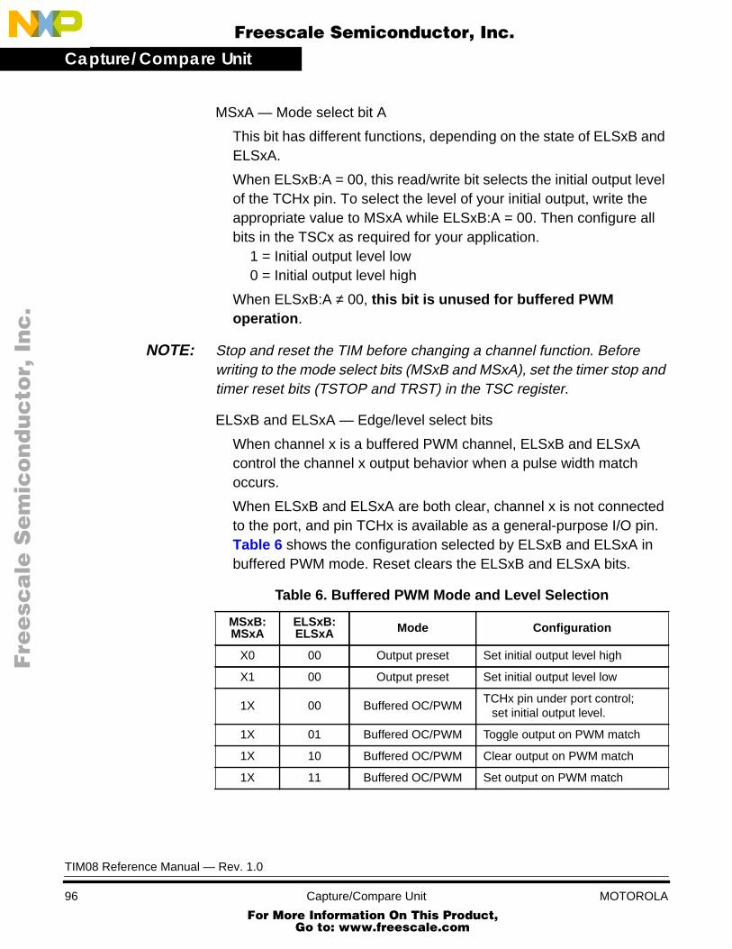
Capture/Compare Unit
F
ree
sca
le S
em
ico
nd
uc
tor,
I
Freescale Semiconductor, Inc.n
c..
.
MSxA — Mode select bit A
This bit has different functions, depending on the state of ELSxB andELSxA.
When ELSxB:A = 00, this read/write bit selects the initial output levelof the TCHx pin. To select the level of your initial output, write theappropriate value to MSxA while ELSxB:A = 00. Then configure allbits in the TSCx as required for your application.
1 = Initial output level low0 = Initial output level high
When ELSxB:A ≠ 00, this bit is unused for buffered PWMoperation .
NOTE: Stop and reset the TIM before changing a channel function. Beforewriting to the mode select bits (MSxB and MSxA), set the timer stop andtimer reset bits (TSTOP and TRST) in the TSC register.
ELSxB and ELSxA — Edge/level select bits
When channel x is a buffered PWM channel, ELSxB and ELSxAcontrol the channel x output behavior when a pulse width matchoccurs.
When ELSxB and ELSxA are both clear, channel x is not connectedto the port, and pin TCHx is available as a general-purpose I/O pin.Table 6 shows the configuration selected by ELSxB and ELSxA inbuffered PWM mode. Reset clears the ELSxB and ELSxA bits.
Table 6. Buffered PWM Mode and Level Selection
MSxB:MSxA
ELSxB:ELSxA Mode Configuration
X0 00 Output preset Set initial output level high
X1 00 Output preset Set initial output level low
1X 00 Buffered OC/PWMTCHx pin under port control;
set initial output level.
1X 01 Buffered OC/PWM Toggle output on PWM match
1X 10 Buffered OC/PWM Clear output on PWM match
1X 11 Buffered OC/PWM Set output on PWM match
TIM08 Reference Manual — Rev. 1.0
96 Capture/Compare Unit MOTOROLA For More Information On This Product,
Go to: www.freescale.com

Capture/Compare UnitBuffered Pulse Width Modulation (PWM) Functions
F
ree
sca
le S
em
ico
nd
uc
tor,
I
Freescale Semiconductor, Inc.n
c..
.
TOVx — Toggle on overflow
When channel x is a buffered or unbuffered OC/PWM channel, thisread/write bit controls the behavior of the channel x output when thetimer counter overflows. Reset clears the TOVx bit.
1 = Channel x pin toggles on timer counter overflow0 = Channel x pin does not toggle on timer counter overflow
NOTE: When TOVx is set, a timer counter overflow takes precedence over achannel x output compare if both occur at the same time.
CHxMAX — PWM 100% duty cycle
This read/write bit forces the duty cycle of buffered and unbufferedPWM signals to 100%. As Figure 38 shows, the CHxMAX bit takeseffect in the cycle after it is set or cleared. The output stays at the100% duty cycle level until the cycle after CHxMAX is cleared.CHxMAX affects only the logic level of the channel x pin; pulse widthmatches can continue to occur and set the channel x flag. Resetclears the CHxMAX bit.
Figure 38. CHxMAX Latency
PULSE WIDTH MATCH
TIMER OVERFLOW
TCHx
PERIOD
CHxMAX
TIM08 Reference Manual — Rev. 1.0
MOTOROLA Capture/Compare Unit 97 For More Information On This Product,
Go to: www.freescale.com

Capture/Compare Unit
F
ree
sca
le S
em
ico
nd
uc
tor,
I
Freescale Semiconductor, Inc.n
c..
.
Timer ChannelRegisters
These read/write registers are used as the 16-bit compare register forPWM functions. These registers contain the pulse width match value forthe PWM function. The state of the channel registers after reset isunknown.
In buffered PWM mode (MSxB = 1), pulse width matches are inhibitedbetween writes to TCHxH and TCHxL of the active channel. Thisprevents another match from occurring until the new pulse width valueis written. Output compares are allowed between writes to TCHxH andTCHxL of the inactive channel. The STHX instruction can be used towrite to TCHxH:L.
If a timer channel register is not used for a PWM function, it can be usedas a storage location.
TIM08 Reference Manual — Rev. 1.0
98 Capture/Compare Unit For More Information On This Prod
Go to: www.freescale.com
MOTOROLA
uct,
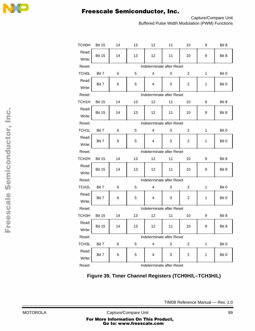
Capture/Compare UnitBuffered Pulse Width Modulation (PWM) Functions
F
ree
sca
le S
em
ico
nd
uc
tor,
I
Freescale Semiconductor, Inc.n
c..
.
Figure 39. Timer Channel Registers (TCH0H/L–TCH3H/L)
TCH0H Bit 15 14 13 12 11 10 9 Bit 8
Read:Bit 15 14 13 12 11 10 9 Bit 8
Write:
Reset: Indeterminate after Reset
TCH0L Bit 7 6 5 4 3 2 1 Bit 0
Read:Bit 7 6 5 4 3 2 1 Bit 0
Write:
Reset: Indeterminate after Reset
TCH1H Bit 15 14 13 12 11 10 9 Bit 8
Read:Bit 15 14 13 12 11 10 9 Bit 8
Write:
Reset: Indeterminate after Reset
TCH1L Bit 7 6 5 4 3 2 1 Bit 0
Read:Bit 7 6 5 4 3 2 1 Bit 0
Write:
Reset: Indeterminate after Reset
TCH2H Bit 15 14 13 12 11 10 9 Bit 8
Read:Bit 15 14 13 12 11 10 9 Bit 8
Write:
Reset: Indeterminate after Reset
TCH2L Bit 7 6 5 4 3 2 1 Bit 0
Read:Bit 7 6 5 4 3 2 1 Bit 0
Write:
Reset: Indeterminate after Reset
TCH3H Bit 15 14 13 12 11 10 9 Bit 8
Read:Bit 15 14 13 12 11 10 9 Bit 8
Write:
Reset: Indeterminate after Reset
TCH3L Bit 7 6 5 4 3 2 1 Bit 0
Read:Bit 7 6 5 4 3 2 1 Bit 0
Write:
Reset: Indeterminate after Reset
TIM08 Reference Manual — Rev. 1.0
MOTOROLA Capture/Compare Unit 99 For More Information On This Product,
Go to: www.freescale.com

Capture/Compare Unit
F
ree
sca
le S
em
ico
nd
uc
tor,
I
Freescale Semiconductor, Inc.n
c..
.
TIM08 Reference Manual — Rev. 1.0
100 Capture/Compare Unit For More Information On This Prod
Go to: www.freescale.com
MOTOROLA
uct,
F
ree
sca
le S
em
ico
nd
uc
tor,
IFreescale Semiconductor, Inc.
nc
...
Interrupts
Contents
Introduction . . . . . . . . . . . . . . . . . . . . . . . . . . . . . . . . . . . . . . . . . . . .101
Interrupts . . . . . . . . . . . . . . . . . . . . . . . . . . . . . . . . . . . . . . . . . . . . .102
Timer DMA Select Register (TDMA) . . . . . . . . . . . . . . . . . . . . . . . .102
CPU Interrupts . . . . . . . . . . . . . . . . . . . . . . . . . . . . . . . . . . . . . . . . .104Timer Overflow Timing . . . . . . . . . . . . . . . . . . . . . . . . . . . . . . . .105Input Capture Timing . . . . . . . . . . . . . . . . . . . . . . . . . . . . . . . . . .105Output Compare/PWM Timing . . . . . . . . . . . . . . . . . . . . . . . . . .109
DMA Service Requests . . . . . . . . . . . . . . . . . . . . . . . . . . . . . . . . . .111Input Capture Timing . . . . . . . . . . . . . . . . . . . . . . . . . . . . . . . . . .111Output Compare/PWM Timing . . . . . . . . . . . . . . . . . . . . . . . . . .113
Introduction
The TIM is capable of generating one interrupt for the timer counteroverflow, and one for each of the channels. These interrupts can bemasked by clearing the Interrupt Enable bit for each interrupt source.See Timer Status and Control Register for more information on settingup the timer counter overflow interrupt. See Timer Channel Status andControl Registers , Timer Channel Status and Control Registers ,Timer Channel Status and Control Registers , Timer Channel Statusand Control Registers , and Timer Channel Status and ControlRegisters for more information on setting up interrupts for each of theTIM channels.
NOTE: The TIM can be implemented with two, four, six or eight channels. Thismanual will show the 4-channel version, as implemented in theMC68HC708XL36.
TIM08 Reference Manual — Rev. 1.0
MOTOROLA Interrupts 101 For More Information On This Product,
Go to: www.freescale.com

Interrupts
F
ree
sca
le S
em
ico
nd
uc
tor,
I
Freescale Semiconductor, Inc.n
c..
.
Interrupts
Each interrupt can be directed to the central processor unit (CPU08),and the channel interrupts can generate service requests directed to thedirect memory access (DMA) module for processing, if available. SeeTimer DMA Select Register (TDMA) for more information on selectingthe interrupt destination for each timer channel.
NOTE: DMA service requests cannot be enabled for buffered OC/PWMoperation. This could cause incorrect flag clearing.
Timer DMA Select Register (TDMA)
The timer DMA register selects either the CPU or the DMA module toservice TIM interrupts. These bits are cleared on reset, selecting theCPU to process interrupts.
NOTE: This register is available only on microcontrollers with a DMA module. Ifno DMA module is included, do not enable the bits described in Figure40. If those bits are enabled, no CPU interrupts for that channel will begenerated or serviced.
NOTE: The TIM can be implemented with two, four, six or eight channels. Thismanual will show the 4-channel version, as implemented in theMC68HC708XL36..
Figure 40. Timer DMA Select Register (TDMA)
TDMA 7 6 5 4 3 2 1 0
Read: 0 0 0 0DMA3S DMA2S DMA1S DMA0S
Write:
Reset: 0 0 0 0 0 0 0 0
TIM08 Reference Manual — Rev. 1.0
102 Interrupts MOTOROLA For More Information On This Product,
Go to: www.freescale.com

InterruptsTimer DMA Select Register (TDMA)
F
ree
sca
le S
em
ico
nd
uc
tor,
I
Freescale Semiconductor, Inc.n
c..
.
DMA3S — DMA channel 3 select
This read/write bit enables the DMA to process TIM interrupts ontimer channel 3. Reset clears the DMA3S bit.
1 = Timer channel 3 generates DMA service requests0 = Timer channel 3 generates CPU interrupt requests
DMA2S — DMA channel 2 select
This read/write bit enables the DMA to process TIM interrupts ontimer channel 2. Reset clears the DMA2S bit.
1 = Timer channel 2 generates DMA service requests0 = Timer channel 2 generates CPU interrupt requests
DMA1S — DMA channel 1 select
This read/write bit enables the DMA to process TIM interrupts ontimer channel 1. Reset clears the DMA1S bit.
1 = Timer channel 1 generates DMA service requests0 = Timer channel 1 generates CPU interrupt requests
DMA0S — DMA channel 0 select
This read/write bit enables the DMA to process TIM interrupts ontimer channel 0. Reset clears the DMA0S bit.
1 = Timer channel 0 generates DMA service requests0 = Timer channel 0 generates CPU interrupt requests
TIM08 Reference Manual — Rev. 1.0
MOTOROLA Interrupts 103 For More Information On This Product,
Go to: www.freescale.com

Interrupts
F
ree
sca
le S
em
ico
nd
uc
tor,
I
Freescale Semiconductor, Inc.n
c..
.
CPU Interrupts
The TIM provides interrupt sources to the CPU08 through the systemintegration module (SIM). The SIM receives all interrupt requests for theCPU and decodes interrupt priorities when multiple requests arereceived. The SIM is different on each microcontroller, and theinterrupt priorities can change. A common TIM interrupt priorityscheme, as implemented on the MC68HC708XL36, is described inthis section. See the applicable technical data book for the correctinterrupt priority.
NOTE: The TIM can be implemented with two, four, six or eight channels. Thismanual will show the 4-channel version, as implemented in theMC68HC708XL36.
If more than one TIM interrupt is received by the SIM, the CH0 interruptis processed first, followed by CH1, CH2, and CH3 interrupts, with thetimer overflow interrupt processed last. The TIM channels will provideinterrupts to the CPU if the associated DMA select bit is cleared, asdiscussed in Timer DMA Select Register (TDMA) .
The interrupt flags (TOF, CH0F, CH1F, CH2F, and CH3F) are set andcleared regardless of the value of the interrupt enable bits (TOE, CH0IE,CH1IE, CH2IE and CH3IE). The interrupt flags are set when a timeroverflow, input capture, output compare, or PWM match occurs. Eachinterrupt flag is cleared by reading the interrupt flag while it is set, andthen writing a logic 0 to the flag. If another flag has been received
Table 7. TIM Interrupt Priority
Source Local Mask GlobalMask Vector Address
CH0F CH0IE
I
$FFF4–$FFF5
CH1F CH1IE $FFF2–$FFF3
CH2F CH2IE $FFF0–$FFF1
CH3F CH3IE $FFEE–$FFEF
TOF TOE $FFEC–$FFED
TIM08 Reference Manual — Rev. 1.0
104 Interrupts MOTOROLA For More Information On This Product,
Go to: www.freescale.com

InterruptsCPU Interrupts
F
ree
sca
le S
em
ico
nd
uc
tor,
I
Freescale Semiconductor, Inc.n
c..
.
between the read and write of the flag, the flag will not be cleared,indicating that another interrupt has occurred.
If the interrupt enable bit is set for a particular flag, a CPU interrupt willbe generated.
Timer OverflowTiming
Figure 41 shows the timing relationships between the MCU bus clocks,the 16-bit timer counter, and the timer overflow flag and interrupt. In thisexample, the modulo counter is programmed to overflow at $0054. Thecounter clock is running at the fastest clock rate, which is the samefrequency as IT12. The counter value changes on the falling edge ofIT12. When the counter reaches the TMOD value, TOF is set at the nextfalling edge of IT12. When TOF is set, the TCHx pin is toggled if TOVxis set in the corresponding TSCx register. TOF also generates the timeroverflow interrupt signal to the CPU08. As long as TOF = 1, the interruptis pending. The interrupt is cleared by clearing TOF: read TOF = 1, thenwrite TOF = 0.
Figure 41 shows another example of a timer overflow occurring. In thisexample, the counter clock is slower than the bus clock. Notice that onthe counter overflow, the TOF is set on the falling edge of IT12 followingthe TMOD match. This immediately resets the timer counter to 0.
Input CaptureTiming
Figure 43 shows the timing relationship between the bus clocks, thecounter, and the input capture circuit for a CPU interrupts on timerchannel 1. A change on the TCH1 input pin occurring before the fallingedge of IT12 is recognized by the input capture circuit. On the next fallingedge of IT12, CH1F is set and the channel 1 CPU interrupt signal,timintcx, is asserted. On the falling edge of IT23, the value of the counteris latched into TCH1. As long as CH1F = 1, the interrupt is pending. Theinterrupt is cleared by clearing CH1F: read CH1F = 1, then writeCH1F = 0.
TIM08 Reference Manual — Rev. 1.0
MOTOROLA Interrupts 105 For More Information On This Product,
Go to: www.freescale.com
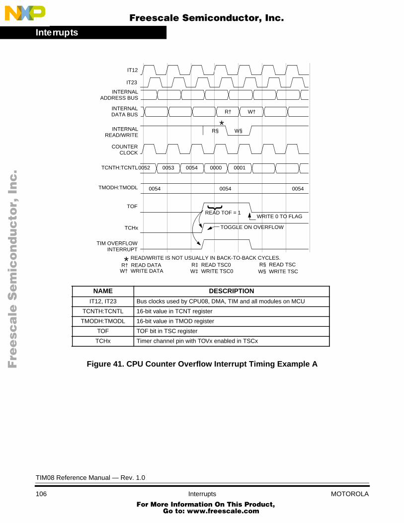
Interrupts
F
ree
sca
le S
em
ico
nd
uc
tor,
I
Freescale Semiconductor, Inc.n
c..
.
Figure 41. CPU Counter Overflow Interrupt Timing Example A
IT12
INTERNAL
COUNTER
TCNTH:TCNTL0052 0053 0054 0000 0001
W§R§INTERNAL
TMODH:TMODL
TCHx TOGGLE ON OVERFLOW
READ TOF = 1WRITE 0 TO FLAG
0054 0054 0054
R† W†
{TOF
*
INTERNAL
IT23
READ/WRITE IS NOT USUALLY IN BACK-TO-BACK CYCLES.R†
W† WRITE DATAREAD DATA* R‡
W‡R§W§
READ TSC0WRITE TSC0
READ TSCWRITE TSC
NAME DESCRIPTION
IT12, IT23 Bus clocks used by CPU08, DMA, TIM and all modules on MCU
TCNTH:TCNTL 16-bit value in TCNT register
TMODH:TMODL 16-bit value in TMOD register
TOF TOF bit in TSC register
TCHx Timer channel pin with TOVx enabled in TSCx
TIM OVERFLOW
ADDRESS BUS
DATA BUS
READ/WRITE
CLOCK
INTERRUPT
TIM08 Reference Manual — Rev. 1.0
106 Interrupts MOTOROLA For More Information On This Product,
Go to: www.freescale.com

InterruptsCPU Interrupts
F
ree
sca
le S
em
ico
nd
uc
tor,
I
Freescale Semiconductor, Inc.n
c..
.
Figure 42. CPU Counter Overflow Interrupt Timing Example B
IT12
INTERNAL
COUNTER
TCNTH:TCNTL 0053 0054 0000
W§R§INTERNAL
TMODH:TMODL
TCHx TOGGLE ON OVERFLOW
READ TOF = 1WRITE 0 TO FLAG
0054 0054
R† W†
{TOF
*
INTERNAL
IT23
READ/WRITE IS NOT USUALLY IN BACK-TO-BACK CYCLES.R†
W† WRITE DATAREAD DATA* R§
W§READ TSCWRITE TSC
NAME DESCRIPTION
IT12, IT23 Bus clocks used by CPU08, DMA, TIM and all modules on MCU
TCNTH:TCNTL 16-bit value in TCNT register
TMODH:TMODL 16-bit value in TMOD register
TOF TOF bit in TSC register
TCHx Timer channel pin with TOVx enabled in TSCx
0001
TIM OVERFLOW
CLOCK
INTERRUPT
READ/WRITE
DATA BUS
ADDRESS BUS
TIM08 Reference Manual — Rev. 1.0
MOTOROLA Interrupts 107 For More Information On This Product,
Go to: www.freescale.com
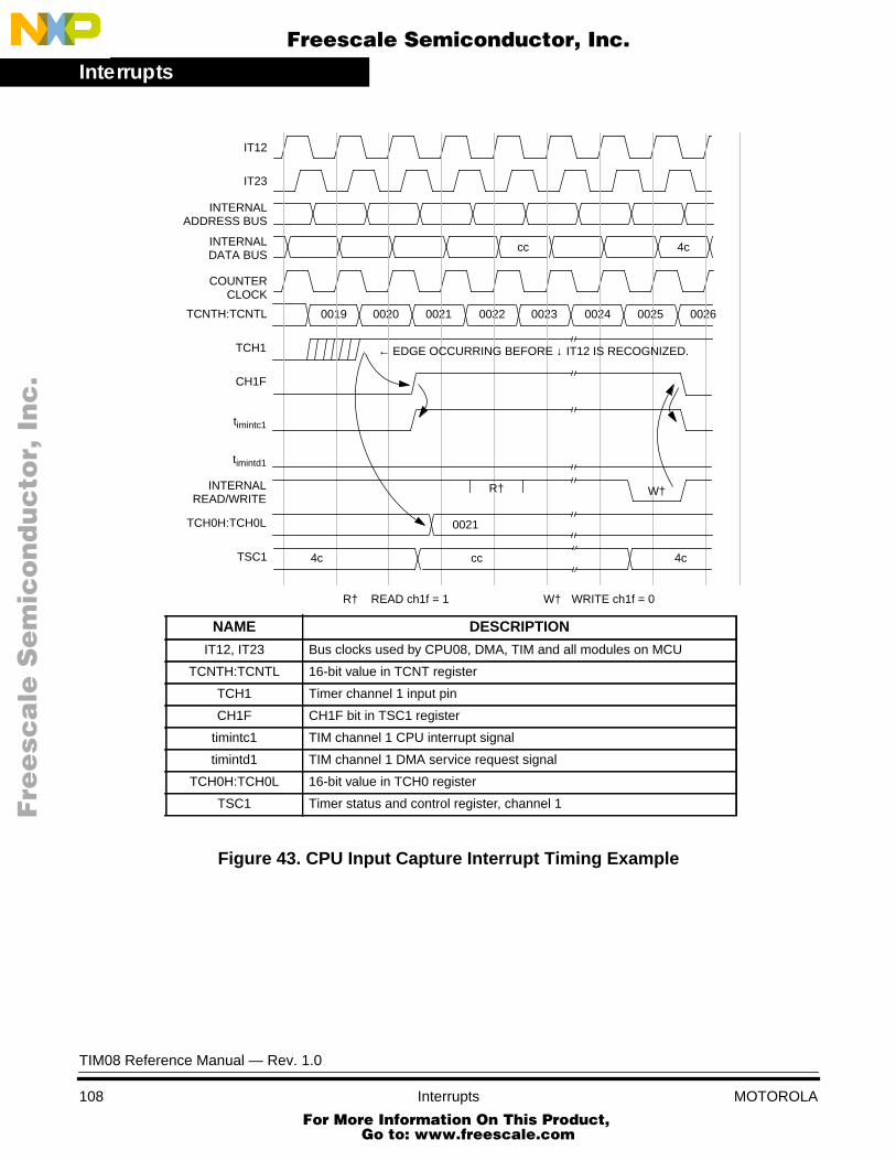
Interrupts
F
ree
sca
le S
em
ico
nd
uc
tor,
I
Freescale Semiconductor, Inc.n
c..
.
Figure 43. CPU Input Capture Interrupt Timing Example
NAME DESCRIPTION
IT12, IT23 Bus clocks used by CPU08, DMA, TIM and all modules on MCU
TCNTH:TCNTL 16-bit value in TCNT register
TCH1 Timer channel 1 input pin
CH1F CH1F bit in TSC1 register
timintc1 TIM channel 1 CPU interrupt signal
timintd1 TIM channel 1 DMA service request signal
TCH0H:TCH0L 16-bit value in TCH0 register
TSC1 Timer status and control register, channel 1
IT12
IT23
INTERNAL
INTERNAL
COUNTER
TCNTH:TCNTL 0019 0020 0021 0022 0023 0024 0025 0026
cc 4c
TCH1
CH1F
timintc1
timintd1
INTERNAL
TCH0H:TCH0L
W†
0021
R†
TSC1 4c cc 4c
R† W†READ ch1f = 1 WRITE ch1f = 0
READ/WRITE
CLOCK
DATA BUS
ADDRESS BUS
← EDGE OCCURRING BEFORE ↓ IT12 IS RECOGNIZED.
TIM08 Reference Manual — Rev. 1.0
108 Interrupts MOTOROLA For More Information On This Product,
Go to: www.freescale.com

InterruptsCPU Interrupts
F
ree
sca
le S
em
ico
nd
uc
tor,
I
Freescale Semiconductor, Inc.n
c..
.
OutputCompare/PWMTiming
Figure 44 shows the timing relationships between the MCU bus clocks,the 16-bit timer counter, and the timer output compare/PWM match flagand interrupt. In this example, the OC/PWM match is programmed tooccur at $0050, and the modulo counter is programmed to overflow at$0054. The counter clock is running at the fastest clock rate, which is thesame frequency as IT12. The counter value changes on the falling edgeof IT12. When the counter reaches the TCH0 value ($0050), CH0F is setat the next falling edge of IT12. When CH0F is set, the TCH0 pin iscleared, as specified in the TSC0 register. CH0F also generates the TIMchannel 0 CPU interrupt signal, timintc0, to the CPU08. While CH0F = 1,the interrupt is pending. The interrupt is cleared by clearing CH0F: readCH0F = 1, then write CH0F = 0. When the counter reaches the TMODvalue, TOF is set, TCH0 toggles, and the timer overflow interrupt signalis asserted, as described in Timer Overflow Timing .
TIM08 Reference Manual — Rev. 1.0
MOTOROLA Interrupts 109 For More Information On This Product,
Go to: www.freescale.com
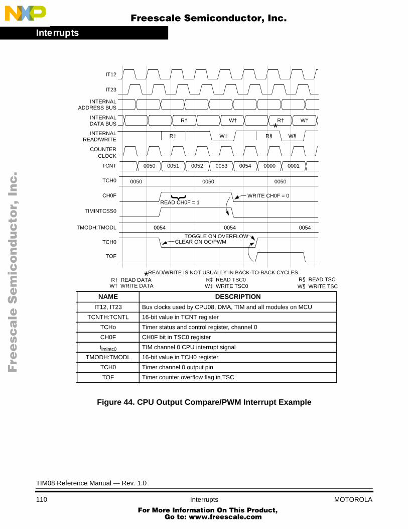
Interrupts
F
ree
sca
le S
em
ico
nd
uc
tor,
I
Freescale Semiconductor, Inc.n
c..
.
Figure 44. CPU Output Compare/PWM Interrupt Example
IT12
INTERNAL
INTERNAL
COUNTER
TCNT 0050 0051 0052 0053 0054 0000 0001
W‡
R†
W§R‡ R§INTERNAL
TCH0
CH0F
TIMINTCSS0
TMODH:TMODL
TCH0 CLEAR ON OC/PWMTOGGLE ON OVERFLOW
0050 0050 0050
READ CH0F = 1WRITE CH0F = 0
0054 0054 0054
W† R† W†
{
TOF
*
NAME DESCRIPTION
IT12, IT23 Bus clocks used by CPU08, DMA, TIM and all modules on MCU
TCNTH:TCNTL 16-bit value in TCNT register
TCHo Timer status and control register, channel 0
CH0F CH0F bit in TSC0 register
timintc0 TIM channel 0 CPU interrupt signal
TMODH:TMODL 16-bit value in TCH0 register
TCH0 Timer channel 0 output pin
TOF Timer counter overflow flag in TSC
IT23
READ/WRITE IS NOT USUALLY IN BACK-TO-BACK CYCLES.R†
W† WRITE DATAREAD DATA* R‡
W‡R§W§
READ TSC0WRITE TSC0
READ TSCWRITE TSC
ADDRESS BUS
DATA BUS
READ/WRITE
CLOCK
TIM08 Reference Manual — Rev. 1.0
110 Interrupts MOTOROLA For More Information On This Product,
Go to: www.freescale.com

InterruptsDMA Service Requests
F
ree
sca
le S
em
ico
nd
uc
tor,
I
Freescale Semiconductor, Inc.n
c..
.
DMA Service Requests
NOTE: DMA service requests are available only on microcontrollers with a DMAmodule. If no DMA module is included, do not enable the bits describedin Figure 40 . If those bits are enabled, no CPU interrupts for thatchannel will be generated or serviced.
The TIM provides service requests to the DMA. The DMA servicerequest priorities are determined by the DMA channel assignment. TheTIM channels will provide service requests to the DMA if the associatedDMA select bit is set, as discussed in Timer DMA Select Register(TDMA).
NOTE: The TIM can be implemented with two, four, six or eight channels. Thismanual will show the 4-channel version, as implemented in theMC68HC708XL36.
The interrupt flags (CH0F, CH1F, CH2F, and CH3F) are set and clearedregardless of the value of the interrupt enable bits (CH0IE, CH1IE,CH2IE, and CH3IE). The interrupt flags are set when an input capture oroutput compare occurs. Each interrupt flag is cleared by reading orwriting to the low byte of the associated channel data register (TCHxL).Reading or writing the interrupt flag will have no affect on the conditionof the flag.
If the interrupt enable bit is set for a particular flag, a DMA servicerequest will be generated.
Input CaptureTiming
Figure 45 shows the timing relationship between the bus clocks, thecounter, and the input capture circuit for a DMA service request on timerchannel 3. A change on the TCH3 input pin occurring before the fallingedge of IT12 is recognized by the input capture circuit. On the next fallingedge of IT12, CH3F is set and the channel 3 DMA service request signal,timintdx, is asserted. On the falling edge of IT23, the value of the counteris latched into TCH3. As long as CH3F = 1, the service request ispending. The service request is cleared when the DMA reads the lowbyte of the channel register, TCH3L. A write to TCH3L will also clear the
TIM08 Reference Manual — Rev. 1.0
MOTOROLA Interrupts 111 For More Information On This Product,
Go to: www.freescale.com
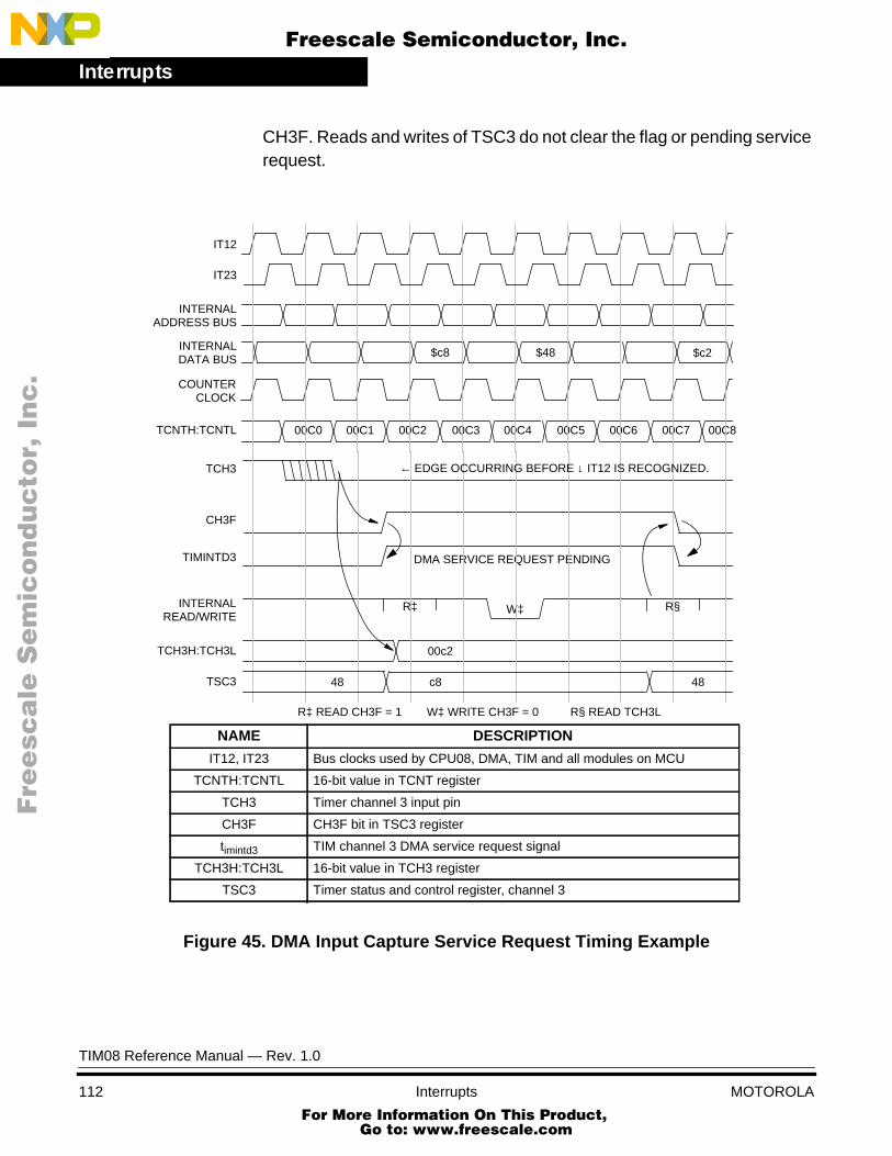
Interrupts
F
ree
sca
le S
em
ico
nd
uc
tor,
I
Freescale Semiconductor, Inc.n
c..
.
CH3F. Reads and writes of TSC3 do not clear the flag or pending servicerequest.
Figure 45. DMA Input Capture Service Request Timing Example
NAME DESCRIPTION
IT12, IT23 Bus clocks used by CPU08, DMA, TIM and all modules on MCU
TCNTH:TCNTL 16-bit value in TCNT register
TCH3 Timer channel 3 input pin
CH3F CH3F bit in TSC3 register
timintd3 TIM channel 3 DMA service request signal
TCH3H:TCH3L 16-bit value in TCH3 register
TSC3 Timer status and control register, channel 3
IT12
INTERNAL
INTERNAL
COUNTER
TCNTH:TCNTL 00C0 00C1 00C2 00C3 00C4 00C5 00C6 00C7 00C8
IT23
TCH3
CH3F
TIMINTD3
INTERNAL
TCH3H:TCH3L
W‡
00c2
R‡ R§
DMA SERVICE REQUEST PENDING
TSC3 c848 48
R‡ READ CH3F = 1 W‡ WRITE CH3F = 0 R§ READ TCH3L
$c2$c8 $48
ADDRESS BUS
DATA BUS
CLOCK
READ/WRITE
← EDGE OCCURRING BEFORE ↓ IT12 IS RECOGNIZED.
TIM08 Reference Manual — Rev. 1.0
112 Interrupts MOTOROLA For More Information On This Product,
Go to: www.freescale.com
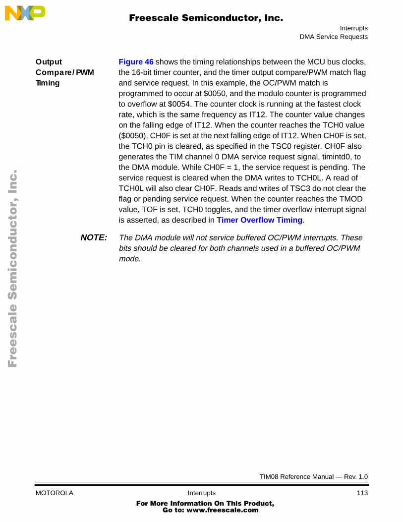
InterruptsDMA Service Requests
F
ree
sca
le S
em
ico
nd
uc
tor,
I
Freescale Semiconductor, Inc.n
c..
.
OutputCompare/PWMTiming
Figure 46 shows the timing relationships between the MCU bus clocks,the 16-bit timer counter, and the timer output compare/PWM match flagand service request. In this example, the OC/PWM match isprogrammed to occur at $0050, and the modulo counter is programmedto overflow at $0054. The counter clock is running at the fastest clockrate, which is the same frequency as IT12. The counter value changeson the falling edge of IT12. When the counter reaches the TCH0 value($0050), CH0F is set at the next falling edge of IT12. When CH0F is set,the TCH0 pin is cleared, as specified in the TSC0 register. CH0F alsogenerates the TIM channel 0 DMA service request signal, timintd0, tothe DMA module. While CH0F = 1, the service request is pending. Theservice request is cleared when the DMA writes to TCH0L. A read ofTCH0L will also clear CH0F. Reads and writes of TSC3 do not clear theflag or pending service request. When the counter reaches the TMODvalue, TOF is set, TCH0 toggles, and the timer overflow interrupt signalis asserted, as described in Timer Overflow Timing .
NOTE: The DMA module will not service buffered OC/PWM interrupts. Thesebits should be cleared for both channels used in a buffered OC/PWMmode.
TIM08 Reference Manual — Rev. 1.0
MOTOROLA Interrupts 113 For More Information On This Product,
Go to: www.freescale.com
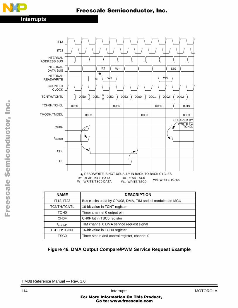
Interrupts
F
ree
sca
le S
em
ico
nd
uc
tor,
I
Freescale Semiconductor, Inc.n
c..
.
Figure 46. DMA Output Compare/PWM Service Request Example
NAME DESCRIPTION
IT12, IT23 Bus clocks used by CPU08, DMA, TIM and all modules on MCU
TCNTH:TCNTL 16-bit value in TCNT register
TCH0 Timer channel 0 output pin
CH0F CH0F bit in TSC0 register
timintd0 TIM channel 0 DMA service request signal
TCH0H:TCH0L 16-bit value in TCH0 register
TSC0 Timer status and control register, channel 0
IT12
COUNTER
TCNTH:TCNTL 0050 0051 0052 0053 0000 0001 0002
TCH0H:TCH0L
TMODH:TMODL
0050 0050 0050 0019
0053 0053 0053
R†
W†
WRITE TSC0 DATAREAD TSC0 DATA
INTERNAL
INTERNAL
R†
W§R‡INTERNAL
CH0F
timintd0
TCH0
TOF
CLEARED BYWRITE TO
R‡W‡
W§ WRITE TCH0LWRITE TSC0READ TSC0
W‡
W†
$19
READ/WRITE IS NOT USUALLY IN BACK-TO-BACK CYCLES.*
*
IT23
TCH0L
CLOCK
ADDRESS BUS
DATA BUS
READ/WRITE
0003
TIM08 Reference Manual — Rev. 1.0
114 Interrupts MOTOROLA For More Information On This Product,
Go to: www.freescale.com
F
ree
sca
le S
em
ico
nd
uc
tor,
IFreescale Semiconductor, Inc.
nc
...
Special Modes
Contents
Introduction . . . . . . . . . . . . . . . . . . . . . . . . . . . . . . . . . . . . . . . . . . . .115
Wait Mode . . . . . . . . . . . . . . . . . . . . . . . . . . . . . . . . . . . . . . . . . . . .116
Stop Mode . . . . . . . . . . . . . . . . . . . . . . . . . . . . . . . . . . . . . . . . . . . .116
Monitor Mode . . . . . . . . . . . . . . . . . . . . . . . . . . . . . . . . . . . . . . . . . .117
Introduction
In addition to the user mode, the M68HC08 Family of microcontrollerssupports several other operating modes. The function of the TIM isdescribed for wait, stop, and monitor modes.
TIM08 Reference Manual — Rev. 1.0
MOTOROLA Special Modes 115 For More Information On This Product,
Go to: www.freescale.com
Special Modes
F
ree
sca
le S
em
ico
nd
uc
tor,
I
Freescale Semiconductor, Inc.n
c..
.
Wait Mode
Wait mode is entered by executing the WAIT instruction in the CPU08.Wait mode is a low-power mode in which the CPU clocks are stopped,and the bus clocks to the TIM continue to run. The TIM functions areactive and all TIM counters and prescalers continue counting during waitmode. A timer interrupt may cause the CPU08 to exit wait mode ifinterrupts are not masked.
All TIM registers retain their states in wait mode.
If a DMA is available, it can service a TIM interrupt without causing theCPU to have to exit wait mode. This can be used to fill a buffer with inputcapture data or to transmit a buffer full of OC/PWM data. A DMA interruptcan be used to exit the CPU from wait and then to use or refill the bufferdata as needed. This feature allows the MCU to conserve power, avoidlong interrupt service latency, and potentially reduce code size due tofewer necessary interrupt service routines.
Stop Mode
Stop mode is entered by executing the STOP instruction in the CPU08.Stop mode is the lowest power-consumption mode, with the bus clocksstopped to both the CPU08 and the TIM. The MCU remains in STOPmode until the STOP bit is negated by the CPU or by a reset. All TIMcounters and prescalers stop counting while the STOP bit is asserted.
All TIM registers retain their states in stop mode.
TIM08 Reference Manual — Rev. 1.0
116 Special Modes For More Information On This Prod
Go to: www.freescale.com
MOTOROLA
uct,

Special ModesMonitor Mode
F
ree
sca
le S
em
ico
nd
uc
tor,
I
Freescale Semiconductor, Inc.n
c..
.
Monitor Mode
Monitor mode gives access to an on-chip monitor providing basicdebugging facilities through a single wire serial interface to a hostcomputer. The debug monitor provides basic commands to read andwrite the memory contents of the 68HC08 through an interface with ahost computer. The monitor commands can be used to provide all thefeatures normally found in a monitor, such as loading in user code,adding breakpoints, and modifying CPU, peripheral, and I/O registercontents. If the MCU application is designed correctly, the monitor canbe used to debug code in the embedded ROM part.
NOTE: The monitor mode is different on each microcontroller, and the sequenceused to enter this mode may change. monitor mode, as implemented onthe MC68HC708XL36, is described in this section.
On the MC68HC708XL36, monitor mode is entered by placing 2 x VDD
on pin IRQ1/VPP, grounding PTC1, and pulling PTC0 high. Theexecution of an SWI (software interrupt) instruction or the execution of ahardware reset while holding PTA0 high will start the monitor and senda break to the host computer. The communication interface with the hostcomputer is a standard asynchronous communication interface with thetransmitted and received data sent over the same wire. For moreinformation on monitor mode, see the appropriate technical data book.
The TIM is active in monitor mode. Software loaded into RAM by thedebug monitor can access TIM registers and interrupts can be enabledand generated.
TIM08 Reference Manual — Rev. 1.0
MOTOROLA Special Modes 117 For More Information On This Product,
Go to: www.freescale.com

Special Modes
F
ree
sca
le S
em
ico
nd
uc
tor,
I
Freescale Semiconductor, Inc.n
c..
.
TIM08 Reference Manual — Rev. 1.0
118 Special Modes For More Information On This Prod
Go to: www.freescale.com
MOTOROLA
uct,

F
ree
sca
le S
em
ico
nd
uc
tor,
IFreescale Semiconductor, Inc.
nc
...
Applications
Contents
Introduction . . . . . . . . . . . . . . . . . . . . . . . . . . . . . . . . . . . . . . . . . . . .120
General TIM Information . . . . . . . . . . . . . . . . . . . . . . . . . . . . . . . . . .121Input Capture . . . . . . . . . . . . . . . . . . . . . . . . . . . . . . . . . . . . . . .121Output Compare . . . . . . . . . . . . . . . . . . . . . . . . . . . . . . . . . . . . .123PWMs . . . . . . . . . . . . . . . . . . . . . . . . . . . . . . . . . . . . . . . . . . . . .125
PWM Controlled RC Digital to Analog Converter . . . . . . . . . . . . . . .131Analysis . . . . . . . . . . . . . . . . . . . . . . . . . . . . . . . . . . . . . . . . . . . .132Hardware . . . . . . . . . . . . . . . . . . . . . . . . . . . . . . . . . . . . . . . . . . .135Software . . . . . . . . . . . . . . . . . . . . . . . . . . . . . . . . . . . . . . . . . . .135
Servo Loop Motor Control . . . . . . . . . . . . . . . . . . . . . . . . . . . . . . . .139
Using the HC708XL36 DMA with the TIM . . . . . . . . . . . . . . . . . . . .144Functional Description of Program . . . . . . . . . . . . . . . . . . . . . . .146System Resource Configuration . . . . . . . . . . . . . . . . . . . . . . . . .146
TIM08 Reference Manual — Rev. 1.0
MOTOROLA Applications 119 For More Information On This Product,
Go to: www.freescale.com

Applications
F
ree
sca
le S
em
ico
nd
uc
tor,
I
Freescale Semiconductor, Inc.n
c..
.
Introduction
The TIM allows flexible configurations to service a variety of timingapplications. Users familiar with the HC05 16-bit timer modules willdiscover that the TIM provides all the same features (input capture,output compare, interrupt on overflow) with additional functionality. Extrafeatures include configurable channels, buffered/unbuffered PWMcapability in conjunction with a modulo register, toggle on overflow, morecontrol of the timer counter (stop and reset commands), and DMAservicing of the TIM on some devices.
The following applications are discussed in this section:
• General TIM Information
• PWM Controlled RC Digital to Analog Converter
• Servo Loop Motor Control
• Using the HC708XL36 DMA with the TIM
NOTE: All software examples in this section were written for theMC68HC708XL36.
TIM08 Reference Manual — Rev. 1.0
120 Applications MOTOROLA For More Information On This Product,
Go to: www.freescale.com

ApplicationsGeneral TIM Information
F
ree
sca
le S
em
ico
nd
uc
tor,
I
Freescale Semiconductor, Inc.n
c..
.
General TIM Information
The following sections detail the basic functions of the TIM includinginput capture, output compare, unbuffered PWM, and buffered PWM bypresenting the following applications:
• Input capture
• Output compare
• PWMs
Input Capture The input capture function is useful for measuring pulse widths orperiods of signals and for establishing functional time references(delays, state machines, etc.) to external events. The TIM allowsprocessor interrupts or polling on rising and/or falling edges, timereference adjustment (via the modulo register), and time baseadjustment (via the prescaler). The following example illustrates ageneral-purpose input capture routine that will measure the period of anincoming signal. Table 8 details possible resolutions and frequencyranges for each timer prescaler. Range indicates the range of inputfrequencies that can be measured, as determined by the value in themodulo register. Resolution indicates the frequency at which the timercounter is incremented by one bit.
NOTE: Higher input frequencies may be difficult to measure without using aDMA or external circuitry.
Table 8. Range and Resolution for Period Input/Output*
Prescaler Range (Hz) Resolution
1 122 - 8.0 M 125 ns
2 61 - 4.0 M 250 ns
4 30.5 - 2.0 M 500 ns
8 15.3 - 1.0 M 1 µs
16 7.6 - 500 k 2 µs
32 3.8 - 250 k 4 µs
64 1.9 - 125 k 8 µs
* Assumes 8 MHz bus clock, 65K counts max
TIM08 Reference Manual — Rev. 1.0
MOTOROLA Applications 121 For More Information On This Product,
Go to: www.freescale.com
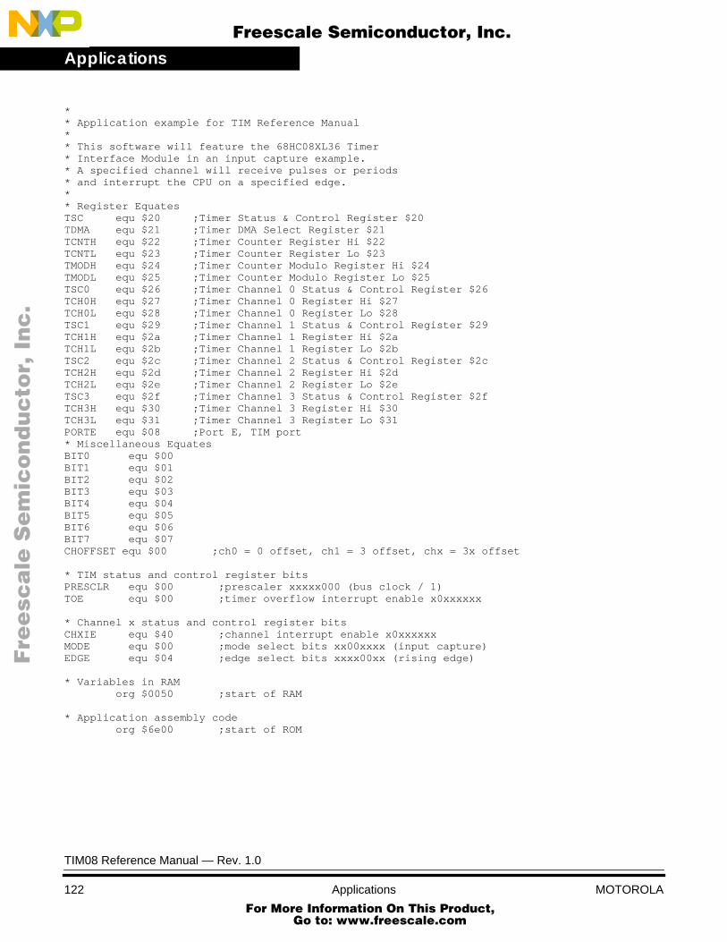
Applications
F
ree
sca
le S
em
ico
nd
uc
tor,
I
Freescale Semiconductor, Inc.n
c..
.
** Application example for TIM Reference Manual** This software will feature the 68HC08XL36 Timer* Interface Module in an input capture example.* A specified channel will receive pulses or periods* and interrupt the CPU on a specified edge.** Register EquatesTSC equ $20 ;Timer Status & Control Register $20TDMA equ $21 ;Timer DMA Select Register $21TCNTH equ $22 ;Timer Counter Register Hi $22TCNTL equ $23 ;Timer Counter Register Lo $23TMODH equ $24 ;Timer Counter Modulo Register Hi $24TMODL equ $25 ;Timer Counter Modulo Register Lo $25TSC0 equ $26 ;Timer Channel 0 Status & Control Register $26TCH0H equ $27 ;Timer Channel 0 Register Hi $27TCH0L equ $28 ;Timer Channel 0 Register Lo $28TSC1 equ $29 ;Timer Channel 1 Status & Control Register $29TCH1H equ $2a ;Timer Channel 1 Register Hi $2aTCH1L equ $2b ;Timer Channel 1 Register Lo $2bTSC2 equ $2c ;Timer Channel 2 Status & Control Register $2cTCH2H equ $2d ;Timer Channel 2 Register Hi $2dTCH2L equ $2e ;Timer Channel 2 Register Lo $2eTSC3 equ $2f ;Timer Channel 3 Status & Control Register $2fTCH3H equ $30 ;Timer Channel 3 Register Hi $30TCH3L equ $31 ;Timer Channel 3 Register Lo $31PORTE equ $08 ;Port E, TIM port* Miscellaneous EquatesBIT0 equ $00BIT1 equ $01BIT2 equ $02BIT3 equ $03BIT4 equ $04BIT5 equ $05BIT6 equ $06BIT7 equ $07CHOFFSET equ $00 ;ch0 = 0 offset, ch1 = 3 offset, chx = 3x offset
* TIM status and control register bitsPRESCLR equ $00 ;prescaler xxxxx000 (bus clock / 1)TOE equ $00 ;timer overflow interrupt enable x0xxxxxx
* Channel x status and control register bitsCHXIE equ $40 ;channel interrupt enable x0xxxxxxMODE equ $00 ;mode select bits xx00xxxx (input capture)EDGE equ $04 ;edge select bits xxxx00xx (rising edge)
* Variables in RAM org $0050 ;start of RAM
* Application assembly code org $6e00 ;start of ROM
TIM08 Reference Manual — Rev. 1.0
122 Applications MOTOROLA For More Information On This Product,
Go to: www.freescale.com
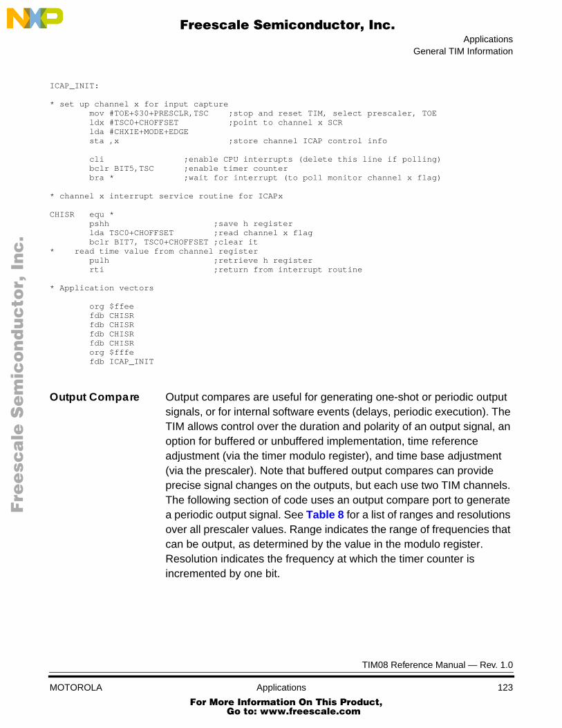
ApplicationsGeneral TIM Information
F
ree
sca
le S
em
ico
nd
uc
tor,
I
Freescale Semiconductor, Inc.n
c..
.
ICAP_INIT:
* set up channel x for input capture mov #TOE+$30+PRESCLR,TSC ;stop and reset TIM, select prescaler, TOE ldx #TSC0+CHOFFSET ;point to channel x SCR lda #CHXIE+MODE+EDGE sta ,x ;store channel ICAP control info
cli ;enable CPU interrupts (delete this line if polling) bclr BIT5,TSC ;enable timer counter bra * ;wait for interrupt (to poll monitor channel x flag)
* channel x interrupt service routine for ICAPx
CHISR equ * pshh ;save h register lda TSC0+CHOFFSET ;read channel x flag bclr BIT7, TSC0+CHOFFSET ;clear it* read time value from channel register pulh ;retrieve h register rti ;return from interrupt routine
* Application vectors
org $ffee fdb CHISR fdb CHISR fdb CHISR fdb CHISR org $fffe fdb ICAP_INIT
Output Compare Output compares are useful for generating one-shot or periodic outputsignals, or for internal software events (delays, periodic execution). TheTIM allows control over the duration and polarity of an output signal, anoption for buffered or unbuffered implementation, time referenceadjustment (via the timer modulo register), and time base adjustment(via the prescaler). Note that buffered output compares can provideprecise signal changes on the outputs, but each use two TIM channels.The following section of code uses an output compare port to generatea periodic output signal. See Table 8 for a list of ranges and resolutionsover all prescaler values. Range indicates the range of frequencies thatcan be output, as determined by the value in the modulo register.Resolution indicates the frequency at which the timer counter isincremented by one bit.
TIM08 Reference Manual — Rev. 1.0
MOTOROLA Applications 123 For More Information On This Product,
Go to: www.freescale.com

Applications
F
ree
sca
le S
em
ico
nd
uc
tor,
I
Freescale Semiconductor, Inc.n
c..
.
** Application example for TIM Reference Manual** This software will feature the 68HC08XL36 Timer* Interface Module in an output compare example.* A signal with 50% duty cycle and specified period* will be generated on a specified channel.** Register EquatesTSC equ $20 ;Timer Status & Control Register $20TDMA equ $21 ;Timer DMA Select Register $21TCNTH equ $22 ;Timer Counter Register Hi $22TCNTL equ $23 ;Timer Counter Register Lo $23TMODH equ $24 ;Timer Counter Modulo Register Hi $24TMODL equ $25 ;Timer Counter Modulo Register Lo $25TSC0 equ $26 ;Timer Channel 0 Status & Control Register $26TCH0H equ $27 ;Timer Channel 0 Register Hi $27TCH0L equ $28 ;Timer Channel 0 Register Lo $28TSC1 equ $29 ;Timer Channel 1 Status & Control Register $29TCH1H equ $2a ;Timer Channel 1 Register Hi $2aTCH1L equ $2b ;Timer Channel 1 Register Lo $2bTSC2 equ $2c ;Timer Channel 2 Status & Control Register $2cTCH2H equ $2d ;Timer Channel 2 Register Hi $2dTCH2L equ $2e ;Timer Channel 2 Register Lo $2eTSC3 equ $2f ;Timer Channel 3 Status & Control Register $2fTCH3H equ $30 ;Timer Channel 3 Register Hi $30TCH3L equ $31 ;Timer Channel 3 Register Lo $31
PORTE equ $08 ;Port E, TIM port
* Miscellaneous EquatesBIT0 equ $00BIT1 equ $01BIT2 equ $02BIT3 equ $03BIT4 equ $04BIT5 equ $05BIT6 equ $06BIT7 equ $07CHOFFSET equ $00 ;ch0 = 0 offset, ch1 = 3 offset, chx = 3x offsetPERHI equ $80 ;16.4ms period, 4.1ms offset from bus clockPERLO equ $00
* TIM status and control register bitsPRESCLR equ $00 ;prescaler xxxxx000 (bus clock / 1)TOE equ $00 ;timer overflow interrupt enable x0xxxxxx
* Channel x status and control register bitsCHIE equ $00 ;channel interrupt enable x0xxxxxxMOD equ $10 ;mode select bits xx00xxxx (output compare)EDG equ $04 ;edge select bits xxxx00xx (toggle output)TOV equ $00 ;toggle on overflow bit xxxxxx0x
* Variables in RAM org $0050 ;start of RAM
* Application assembly code org $6e00 ;start of ROM
TIM08 Reference Manual — Rev. 1.0
124 Applications MOTOROLA For More Information On This Product,
Go to: www.freescale.com
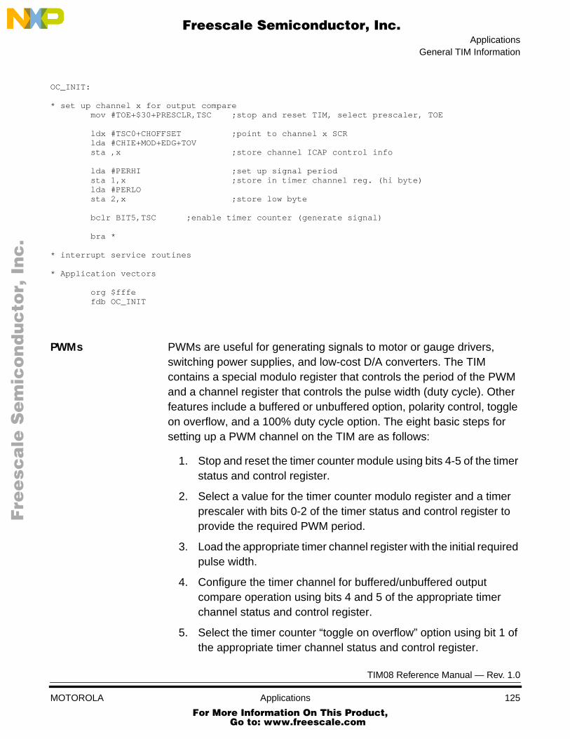
ApplicationsGeneral TIM Information
F
ree
sca
le S
em
ico
nd
uc
tor,
I
Freescale Semiconductor, Inc.n
c..
.
OC_INIT:
* set up channel x for output compare mov #TOE+$30+PRESCLR,TSC ;stop and reset TIM, select prescaler, TOE
ldx #TSC0+CHOFFSET ;point to channel x SCR lda #CHIE+MOD+EDG+TOV sta ,x ;store channel ICAP control info
lda #PERHI ;set up signal period sta 1,x ;store in timer channel reg. (hi byte) lda #PERLO sta 2,x ;store low byte
bclr BIT5,TSC ;enable timer counter (generate signal)
bra *
* interrupt service routines
* Application vectors
org $fffe fdb OC_INIT
PWMs PWMs are useful for generating signals to motor or gauge drivers,switching power supplies, and low-cost D/A converters. The TIMcontains a special modulo register that controls the period of the PWMand a channel register that controls the pulse width (duty cycle). Otherfeatures include a buffered or unbuffered option, polarity control, toggleon overflow, and a 100% duty cycle option. The eight basic steps forsetting up a PWM channel on the TIM are as follows:
1. Stop and reset the timer counter module using bits 4-5 of the timerstatus and control register.
2. Select a value for the timer counter modulo register and a timerprescaler with bits 0-2 of the timer status and control register toprovide the required PWM period.
3. Load the appropriate timer channel register with the initial requiredpulse width.
4. Configure the timer channel for buffered/unbuffered outputcompare operation using bits 4 and 5 of the appropriate timerchannel status and control register.
5. Select the timer counter “toggle on overflow” option using bit 1 ofthe appropriate timer channel status and control register.
TIM08 Reference Manual — Rev. 1.0
MOTOROLA Applications 125 For More Information On This Product,
Go to: www.freescale.com

Applications
F
ree
sca
le S
em
ico
nd
uc
tor,
I
Freescale Semiconductor, Inc.n
c..
.
6. Configure the timer channel to force the output to the “inactive”level on a successful compare (toggle on output compare shouldnot be used) using bits 2 and 3 of the appropriate timer channelstatus and control register.
7. Enable output compare interrupts (if used) using bit 0 of theappropriate timer channel status and control register.
8. Enable the timer counter using bit 5 of the timer status and controlregister.
The following code details a general-purpose unbuffered PWM routine(all parameters are user-selectable).
** This software will feature the 68HC08XL36 Timer* Interface Module in an unbuffered PWM example.* A periodic waveform with specified duty cycle* and period will be generated on a specified* channel.** Register EquatesTSC equ $20 ;Timer Status & Control Register $20TDMA equ $21 ;Timer DMA Select Register $21TCNTH equ $22 ;Timer Counter Register Hi $22TCNTL equ $23 ;Timer Counter Register Lo $23TMODH equ $24 ;Timer Counter Modulo Register Hi $24TMODL equ $25 ;Timer Counter Modulo Register Lo $25TSC0 equ $26 ;Timer Channel 0 Status & Control Register $26TCH0H equ $27 ;Timer Channel 0 Register Hi $27TCH0L equ $28 ;Timer Channel 0 Register Lo $28TSC1 equ $29 ;Timer Channel 1 Status & Control Register $29TCH1H equ $2a ;Timer Channel 1 Register Hi $2aTCH1L equ $2b ;Timer Channel 1 Register Lo $2bTSC2 equ $2c ;Timer Channel 2 Status & Control Register $2cTCH2H equ $2d ;Timer Channel 2 Register Hi $2dTCH2L equ $2e ;Timer Channel 2 Register Lo $2eTSC3 equ $2f ;Timer Channel 3 Status & Control Register $2fTCH3H equ $30 ;Timer Channel 3 Register Hi $30TCH3L equ $31 ;Timer Channel 3 Register Lo $31
PORTE equ $08 ;Port E, TIM port
* Miscellaneous EquatesBIT0 equ $00BIT1 equ $01BIT2 equ $02BIT3 equ $03BIT4 equ $04BIT5 equ $05BIT6 equ $06BIT7 equ $07CHOFFSET equ $00 ;ch0 = 0 offset, ch1 = 3 offset, chx = 3x offsetDUTYHI equ $80 ;50% duty cycleDUTYLO equ $00PERHI equ $FF ;8.2ms periodPERLO equ $FF
TIM08 Reference Manual — Rev. 1.0
126 Applications MOTOROLA For More Information On This Product,
Go to: www.freescale.com

ApplicationsGeneral TIM Information
F
ree
sca
le S
em
ico
nd
uc
tor,
I
Freescale Semiconductor, Inc.n
c..
.
* TIM status and control register bitsPRESCLR equ $00 ;prescaler xxxxx000 (bus clock / 1)TOE equ $00 ;timer overflow interrupt enable x0xxxxxx
* Channel x status and control register bitsCHIE equ $40 ;channel interrupt enable x0xxxxxxMOD equ $10 ;mode select bits xx00xxxx (output compare)EDG equ $0c ;edge select bits xxxx00xx (set output)TOV equ $02 ;toggle on overflow bit xxxxxx0x
* Variables in RAMorg $0050 ;start of RAM
* Application assembly codeorg $6e00 ;start of ROM
UNBUF_INIT:
* set up channel x for unbuffered PWMmov #TOE+$30+PRESCLR, TSC ;stop and reset TIM, select prescaler, TOEldx #TSC0+CHOFFSET ;point to channel x SCR (H reg = 00)lda #CHIE+MOD+EDG+TOV ;enable i, OC, set output, togglesta ,x ;store channel ICAP control infolda #DUTYHI ;specified duty cyclesta 1,x ;store in timer channel reg.lda #DUTYLOsta 2,x
mov #PERHI,TMODH ;store specified periodmov #PERLO,TMODL
cli ;enable CPU interrupts (delete this line if polling)bclr BIT5,TSC ;enable timer counter
bra * ;wait for interrupt (to poll monitor channel x flag)
* channel x interrupt service routine for OCx
CHISR equ *pshh ;save h registerlda TSC0+CHOFFSET ;read channel x flagbclr BIT7,TSC0+CHOFFSET ;clear it
* change duty cycle here (write to channel register)pulh ;retrieve h registerrti ;return from interrupt routine
* Application vectors
org $ffeefdb CHISRfdb CHISRfdb CHISRfdb CHISR
org $fffefdb UNBUF_INIT
TIM08 Reference Manual — Rev. 1.0
MOTOROLA Applications 127 For More Information On This Product,
Go to: www.freescale.com
Applications
F
ree
sca
le S
em
ico
nd
uc
tor,
I
Freescale Semiconductor, Inc.n
c..
.
The limitations of unbuffered PWMs are most apparent during the pulsewidth/duty cycle update process (for example, changing the timerchannel register). The least reliable method is to randomly update thechannel register, which can take up to two full periods to synchronize theoutput. A more reliable method is to update the channel register duringa timer overflow interrupt routine, which can still cause one period ofsynchronization if the pulse width is decreased to 16 bus cycles or less(worst case interrupt latency before channel register update). The mostreliable method is to update the channel register during an outputcompare interrupt routine. However, even this method willunsynchronize the output for one period when changing from a very highduty cycle to a very low duty cycle (for example, the interrupt routinelatency exceeds the toggle and pulse width).
Since there are no infallible unbuffered PWM methodologies, the TIMhas been designed to configure buffered PMW channels, at the trade-offof using two TIM channels. Buffered PWM channels are initialized usingthe same eight steps listed above and are implemented by alternatelywriting one of two timer channel registers. The software must track whichchannel register was last written. The following code details a generalpurpose buffered PWM routine using the TIM (all parameters are userselectable).
TIM08 Reference Manual — Rev. 1.0
128 Applications MOTOROLA For More Information On This Product,
Go to: www.freescale.com
ApplicationsGeneral TIM Information
F
ree
sca
le S
em
ico
nd
uc
tor,
I
Freescale Semiconductor, Inc.n
c..
.
** This software will feature the 68HC08XL36 Timer* Interface Module in an buffered PWM example.* A periodic waveform with specified duty cycle* and period will be generated on a specified* channel.** Register EquatesTSC equ $20 ;Timer Status & Control Register $20TDMA equ $21 ;Timer DMA Select Register $21TCNTH equ $22 ;Timer Counter Register Hi $22TCNTL equ $23 ;Timer Counter Register Lo $23TMODH equ $24 ;Timer Counter Modulo Register Hi $24TMODL equ $25 ;Timer Counter Modulo Register Lo $25TSC0 equ $26 ;Timer Channel 0 Status & Control Register $26TCH0H equ $27 ;Timer Channel 0 Register Hi $27TCH0L equ $28 ;Timer Channel 0 Register Lo $28TSC1 equ $29 ;Timer Channel 1 Status & Control Register $29TCH1H equ $2a ;Timer Channel 1 Register Hi $2aTCH1L equ $2b ;Timer Channel 1 Register Lo $2bTSC2 equ $2c ;Timer Channel 2 Status & Control Register $2cTCH2H equ $2d ;Timer Channel 2 Register Hi $2dTCH2L equ $2e ;Timer Channel 2 Register Lo $2eTSC3 equ $2f ;Timer Channel 3 Status & Control Register $2fTCH3H equ $30 ;Timer Channel 3 Register Hi $30TCH3L equ $31 ;Timer Channel 3 Register Lo $31
PORTE equ $08 ;Port E, TIM port
* Miscellaneous EquatesBIT0 equ $00BIT1 equ $01BIT2 equ $02BIT3 equ $03BIT4 equ $04BIT5 equ $05BIT6 equ $06BIT7 equ $07CHOFFSET equ $00 ;ch0 = 0 offset, ch2 = 6 offsetDUTYHI equ $80 ;50% duty cycleDUTYLO equ $00PERHI equ $FF ;8.2ms periodPERLO equ $FF
* TIM status and control register bitsPRESCLR equ $00 ;prescaler xxxxx000 (bus clock / 1)TOE equ $00 ;timer overflow interrupt enable x0xxxxxx
* Channel x status and control register bitsCHIE equ $40 ;channel interrupt enable x0xxxxxxMOD equ $30 ;mode select bits xx00xxxx (buffered PWM)EDG equ $0c ;edge select bits xxxx00xx (set output)TOV equ $02 ;toggle on overflow bit xxxxxx0x
* Variables in RAMorg $0050 ;start of RAM
track rmb 1
TIM08 Reference Manual — Rev. 1.0
MOTOROLA Applications 129 For More Information On This Product,
Go to: www.freescale.com

Applications
F
ree
sca
le S
em
ico
nd
uc
tor,
I
Freescale Semiconductor, Inc.n
c..
.
* Application assembly codeorg $6e00 ;start of ROM
BUFF_INIT:
* set up channel x for unbuffered PWMbset BIT0,track ;set tracker flag
mov #TOE+$30+PRESCLR,TSC ;stop and reset TIM, select prescaler, TOE
ldx #TSC0+CHOFFSET ;point to channel x SCR (H reg = 00)lda #CHIE+MOD+EDG+TOV ;enable i, buff, set output, togglesta ,x ;store channel OC control info
lda #DUTYHI ;specified duty cyclesta 1,x ;store in timer channel reg.lda #DUTYLOsta 2,x
mov #PERHI,TMODH ;store specified period in MOD reg.mov #PERLO,TMODL
cli ;enable CPU interrupts (delete this line if polling)bclr BIT5,TSC ;enable timer counter (start PWM)
bra * ;wait for interrupt (to poll monitor channel x flag)
* channel x interrupt service routine for OCx
CHISR equ *pshh ;save h registerlda TSC0+CHOFFSET ;read channel x flagbclr BIT7,TSC0+CHOFFSET ;clear itbrset BIT0,track,JUMP ;determine which reg. to updatebset BIT0,track ;set tracker flag
* change duty cycle (write to channel 1 or 3 register)bra EXIT
JUMP bclr BIT0,track ;clear tracker flag* change duty cycle (write to channel 2 or 4 register)EXIT pulh ;retrieve h register
rti ;return from interrupt routine
* Application vectors
org $ffeefdb CHISRfdb CHISRfdb CHISRfdb CHISRorg $fffefdb BUFF_INIT
TIM08 Reference Manual — Rev. 1.0
130 Applications MOTOROLA For More Information On This Product,
Go to: www.freescale.com

ApplicationsPWM Controlled RC Digital to Analog Converter
F
ree
sca
le S
em
ico
nd
uc
tor,
I
Freescale Semiconductor, Inc.n
c..
.
PWM Controlled RC Digital to Analog Converter
Pulse width modulation (PWM) is the process of using signal processingtechniques to control the pulse width of a digital signal. The PWM signalis manipulated by software instructions and can be used in a variety ofapplications. One application is the design of a digital-to-analogconverter (DAC). The PWM signal is sent out of the MCU and directlydrives an RC circuit as shown in Figure 47 . This circuit will produce afiltered average of the PWM signal on the output.
Figure 47. RC Circuit
For example, a 25% duty cycle PWM signal is shown in Figure 48 . The“high” part of the signal is called the pulse width and in this examplerepresents 25% of the PWM period. The “low” part of the signalrepresents 75% of the PWM signal. The entire cycle of the entire PWMsignal is called the “PWM period.” The PWM frequency is 1/(PWMperiod).
Figure 48. 25% Duty Cycle PWM Signal
When a PWM signal is fed into the RC circuit shown in Figure 47 , apseudo DC signal is created at the output of the RC circuit. This signalwill have some low amplitude ripple dependent on the RC time constantof the circuit and the frequency of the PWM signal.
The average DC signal is related to the length of the pulse width of thePWM signal. The equation is as follows:
INR C
OUT
PWM PERIOD
PULSE WIDTH
PWM PULSE
TIM08 Reference Manual — Rev. 1.0
MOTOROLA Applications 131 For More Information On This Product,
Go to: www.freescale.com

Applications
F
ree
sca
le S
em
ico
nd
uc
tor,
I
Freescale Semiconductor, Inc.n
c..
.
Average DC signal = Duty Cycle * (PWM high voltage — PWM lowvoltage)
For example, if there is a 5-volt, 50% duty cycle PWM signal driving theRC circuit in Figure 47 , the average DC out voltage would be 2.5 volts.If the PWM duty cycle was changed to 85%, the average DC outputvoltage would be 4.25 volts. By varying the duty cycle, the user candesign a simple digital-to-analog converter.
Analysis There are four parameters that affect the DC output voltage: thecapacitor, resistor, PWM frequency, and the PWM pulse width. As thepreceding example has shown, the PWM pulse width (duty cycle)directly affects the filtered DC output level. The frequency and the RCtime constant affect the ripple of the output. As the resistor and/or thecapacitor are increased, there will be less ripple on the output due to theincreased time constant of the circuit. Also, as the frequency increases,the ripple's frequency will increase, but its amplitude will decreasebecause the time for the voltage to rise or fall will be shortened.
When a rising voltage pulse is fed into the RC circuit, the output voltageresponds according to the following equation:
where VOUT is the output voltage, VIN is the input voltage, t is time afterpulse, and RC is the time constant.
When a falling voltage pulse is fed into the RC circuit, the output voltageresponds according to the following equation:
Figure 49 illustrates the transient voltage waveform of an RC networkdriven by a PWM signal. In this example, a 10-kHz, 50% duty cycle,5-volt digital signal drives a resistor of 1 k½ and a capacitor of 1µF.
VOUT = VIN – VIN e–t
RC
VOUT = VIN e–t
RC
TIM08 Reference Manual — Rev. 1.0
132 Applications MOTOROLA For More Information On This Product,
Go to: www.freescale.com
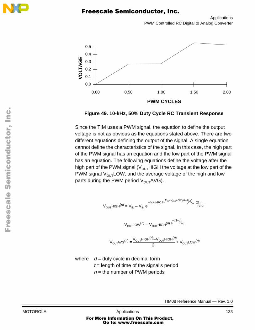
ApplicationsPWM Controlled RC Digital to Analog Converter
F
ree
sca
le S
em
ico
nd
uc
tor,
I
Freescale Semiconductor, Inc.n
c..
.
Figure 49. 10-kHz, 50% Duty Cycle RC Transient Response
Since the TIM uses a PWM signal, the equation to define the outputvoltage is not as obvious as the equations stated above. There are twodifferent equations defining the output of the signal. A single equationcannot define the characteristics of the signal. In this case, the high partof the PWM signal has an equation and the low part of the PWM signalhas an equation. The following equations define the voltage after thehigh part of the PWM signal (VOUTHIGH the voltage at the low part of thePWM signal VOUTLOW, and the average voltage of the high and lowparts during the PWM period VOUTAVG).
where d = duty cycle in decimal formt = length of time of the signal's periodn = the number of PWM periods
0.00 0.50 1.00 1.50 2.00
0.0
0.1
0.2
0.3
0.4
0.5
PWM CYCLES
VO
LTA
GE
VOUTHIGH(n) = VIN – VIN e RC–[tc+(–RC ln( ))]
VIN–VOUTLOW (n–1)VIN
VOUTLOW(n) = VOUTHIGH(n) e RC–t(1–d)
VOUTAVG(n) = + VOUTLOW(n)VOUTHIGH(n)–VOUTHIGH(n)
2
TIM08 Reference Manual — Rev. 1.0
MOTOROLA Applications 133 For More Information On This Product,
Go to: www.freescale.com

Applications
F
ree
sca
le S
em
ico
nd
uc
tor,
I
Freescale Semiconductor, Inc.n
c..
.
Finding the output voltage at a particular time now becomes an iterativeprocess. Write a small program with the preceding equations for youranalysis. For example, use the circuit described earlier: a 5-volt 50%duty cycle, 10-kHz PWM signal driving a 1-k½ resistor and a 1-F capacitornetwork. Find the output voltage after the duty cycle of the second PWMperiod and the average voltage after one PWM period. After calculatingwith t = .0001 and d = 0.5, the following results are shown in Table 9 .
Therefore, the output voltage after the duty cycle of the second PWMperiod is 0.46450009 volts. The average voltage after one PWM periodis 0.23790645 volts. A graph of the output voltage over 60 time periodsis shown in Figure 50 .
Figure 50. 10-kHz, 50% Duty Cycle RC Response
Table 9. Output Voltages
Time Period VOUTHIGH VOUTLOW VOUTAVG
0 0 0 0
1 0.24385288 0.23196003 0.23790645
2 0.46450009 0.44184615 0.45317312
TIM08 Reference Manual — Rev. 1.0
134 Applications MOTOROLA For More Information On This Product,
Go to: www.freescale.com

ApplicationsPWM Controlled RC Digital to Analog Converter
F
ree
sca
le S
em
ico
nd
uc
tor,
I
Freescale Semiconductor, Inc.n
c..
.
Hardware Figure 47 shows that the DAC circuit is designed with an RC network. Ifthe DAC were designed to drive a load, the extra load would change thetime constant of the RC network. This in turn would change the transientand steady state responses. In order to buffer the RC network, feed theoutput into an op amp configured as a voltage follower. Since the inputsto the op amp are very high impedance, they should not affect theresponse of the RC network. The output of the op amp can now drivelarger loads. This circuit is shown in Figure 51 .
Figure 51. Buffered Output
Software The following code initializes the timer for PWM and then enables thetimer to start outputting the PWM signal.
INR C
+VCC
–VEE
OUT+—
TIM08 Reference Manual — Rev. 1.0
MOTOROLA Applications 135 For More Information On This Product,
Go to: www.freescale.com
Applications
F
ree
sca
le S
em
ico
nd
uc
tor,
I
Freescale Semiconductor, Inc.n
c..
.
********************************************************************************************************************************************************* ** Implementation of an unbuffered PWM with the Timer ** ****************************************************************************** ** File Name: UB_PWM.RTN Copyright (c) Motorola 1994 ** ** Curent Revision: 1.00 ** Current Release Level: ESS ** Current Revision Release Date: 03/23/94 ** ** Current Release Written By: Mark Glenewinkel ** Motorola CMCU Applications - Austin, Texas ** ** Assembled Under: IASM08 (P&E Microcomputer Systems, Inc.) Ver.: 1.00 ** ** Documentation File Name: UB_PWM.DOC Revision: 1.00 ** ** Brief Description of Routine Purpose: ** This routine uses the Timer to implement a PWM signal. ** ** Part Family Software Routine Works With: HC08 ** ** Worst Case Execution (Cycles): 28 ** Routine Size (Bytes): 20 ** Stack Space Used (Bytes): 0 ** RAM Used (Bytes): 0 ** ** Global Variables Used: None ** Subroutines Used: None ** ** Full Functional Description of Routine Design: ** In order to setup a PWM waveform, the following must be configured: ** 1) Stop the timer, reset the timer counter (set TSTOP & TRST bits in TSC)** 2) Write to the 16 bit modulo counter to set the PWM period (TMODH:L) ** 3) Write to the 16 bit Output Compare register for the appropriate ** timer channel. This sets the PWM pulse width (TCHxH:L) ** 4) Write to the timer channel status and control register (TSCx) ** Disable the output compare interrupt (CHxIE = 0) ** Configure for unbuffered PWM (MSxB:A = 01) ** Configure to clear output line on PWM match (ELSxB:A = 10) ** Configure overflow to toggle timer channel (TDVx = 1) ** Disable max 100% duty cycle (CHxMAX = 0) ** 5) Enable the timer to start counting (clear TSTOP in TSC) ** ****************************************************************************** ** Update History: ** Rev: Author: Date: Description of Change: ** ---- ------- ----- ---------------------- ** ESS 1.0 Glenewinkel 03/23/94 Original Release ** ********************************************************************************************************************************************************** ** Motorola reserves the right to make changes without further notice to any ** product herein to improve reliability, function, or design. Motorola does ** not assume any liability arising out of the application or use of any ** product, circuit, or software described herein; neither does it convey any*
TIM08 Reference Manual — Rev. 1.0
136 Applications MOTOROLA For More Information On This Product,
Go to: www.freescale.com

ApplicationsPWM Controlled RC Digital to Analog Converter
F
ree
sca
le S
em
ico
nd
uc
tor,
I
Freescale Semiconductor, Inc.n
c..
.
* license under its patent rights nor the rights of others. Motorola ** products are not designed, intended, or authorized for use as components ** in systems intended for surgical implant into the body, or other ** applications intended to support life, or for any other application in ** which the failure of the Motorola product could create a situation where ** personal injury or death may occur. Should Buyer purchase or use Motorola ** products for any such intended or unauthorized application, Buyer shall ** indemnify and hold Motorola and its officers, employees, subsidiaries, ** affiliatees, and distributors harmless against all claims, costs, damages, ** and expenses, and reasonable attorney fees arising out of, directly or ** indirectly, any claim of personal injury or death associated with such ** unintended or unauthorized use, even if such claim alleges that Motorola ** was negligent regarding the design or manufacture of the part. Motorola ** and the Motorola Logo are registered trademarks of Motorola Inc. ** ********************************************************************************************************************************************************** ** Part Specific Framework Includes Section ** *$INCLUDE 'H708XL36.FRK' ;Device specific equates file****************************************************************************** ** Equates for Main Routine ** ****************************************************************************** ** None* ****************************************************************************** ** RAM Definitions for Main Routine ** ****************************************************************************** * org RAM_Start* None* ****************************************************************************** ** Program Initialization ** ** Code needed to initialize processor resources is placed here. ** *****************************************************************************
org EPROM_Start ; start of HC708XL36 EPROM ($6E00)
Start mov #$30,TSC ; stop the timer counter ; reset timer counter
; select prescaler (timclk = busclock)* Write the value for the required PWM frequency* With a 4 MHz bus, $01FF in the modulo register* creates a 7.8125kHz signal or a 128usec period
mov #$01,TMODH ; modulo byte high mov #$FF,TMODL ; modulo byte low
TIM08 Reference Manual — Rev. 1.0
MOTOROLA Applications 137 For More Information On This Product,
Go to: www.freescale.com

Applications
F
ree
sca
le S
em
ico
nd
uc
tor,
I
Freescale Semiconductor, Inc.n
c..
.
* Write the value for the required PWM pulse width* For a 25% pulse width, the pulse width will be equal* to 32usec* Write $0080 to timer channel 0 output compare
mov #$00,TCH0H ; timer channel 0 high mov #$80,TCH0L ; timer channel 0 low
* Write to timer channel 0 status and control reg* CH0E=0, disable output compare interrupt* MS0B:MS0A=01, unbuffered PWM, output compare* ELS0B:ELS0A=10, clear output line on compare* TOV0=1, enable timer counter toggle on overflow* CH0MAX=0, disable max 100% duty cycle
mov #%00011010,TSC0 ; timer CH0 status & ctrl
* Enable the timer - start counter by clearing STOP bit
bclr 5,TSC ; timer status & ctrl
***************************************************************************** ** Main Program Loop ** *****************************************************************************
LOOP nop ; infinite loop while PWM bra LOOP ; is running
***************************************************************************** ** Interrupt Service Routines for Main Routine ** *****************************************************************************
org RESET fdb Start
****************************************************************************
TIM08 Reference Manual — Rev. 1.0
138 Applications MOTOROLA For More Information On This Product,
Go to: www.freescale.com
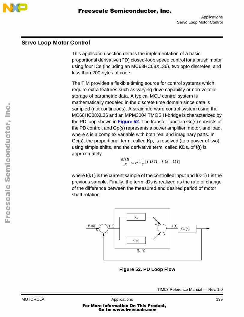
ApplicationsServo Loop Motor Control
F
ree
sca
le S
em
ico
nd
uc
tor,
I
Freescale Semiconductor, Inc.n
c..
.
Servo Loop Motor Control
This application section details the implementation of a basicproportional derivative (PD) closed-loop speed control for a brush motorusing four ICs (including an MC68HC08XL36), two opto discretes, andless than 200 bytes of code.
The TIM provides a flexible timing source for control systems whichrequire extra features such as varying drive capability or non-volatilestorage of parametric data. A typical MCU control system ismathematically modeled in the discrete time domain since data issampled (not continuous). A straightforward control system using theMC68HC08XL36 and an MPM3004 TMOS H-bridge is characterized bythe PD loop shown in Figure 52 . The transfer function Gc(s) consists ofthe PD control, and Gp(s) represents a power amplifier, motor, and load,where s is a complex variable with both real and imaginary parts. InGc(s), the proportional term, called Kp, is resolved (to a power of two)using simple shifts, and the derivative term, called KDs, of f(t) isapproximately
where f(kT) is the current sample of the controlled input and f(k-1)T is theprevious sample. Finally, the term kDs is realized as the rate of changeof the difference between the measured and desired period of motorshaft rotation.
Figure 52. PD Loop Flow
dƒ(t)dt t = kT ≅ 1
Τ[ƒ (kT) – ƒ (k – 1)T]
KP
KDs
GP (s)R (s) ƒ (t) µ (ƒ)
GC (s)
+
–
+
+
TIM08 Reference Manual — Rev. 1.0
MOTOROLA Applications 139 For More Information On This Product,
Go to: www.freescale.com
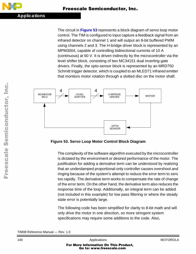
Applications
F
ree
sca
le S
em
ico
nd
uc
tor,
I
Freescale Semiconductor, Inc.n
c..
.
The circuit in Figure 53 represents a block diagram of servo loop motorcontrol. The TIM is configured to input capture a feedback signal from aninfrared detector on channel 1 and will output an 8-bit buffered PWMusing channels 2 and 3. The H-bridge driver block is represented by anMPM3004, capable of controlling bidirectional currents of 10 A(continuous) at 60 V. It is driven indirectly by the microcontroller via thelevel shifter block, consisting of two MC34151 dual inverting gatedrivers. Finally, the opto-sensor block is represented by an MRD750Schmitt trigger detector, which is coupled to an MLED71 infrared emitterthat monitors motor rotation through a slotted disc on the motor shaft.
Figure 53. Servo Loop Motor Control Block Diagram
The complexity of the software algorithm executed by the microcontrolleris dictated by the environment or desired performance of the motor. Thejustification for adding a derivative term can be understood by realizingthat an underdamped proportional-only controller causes overshoot andringing because of the system's attempt to reduce the error term to zerotoo rapidly. The derivative term works to compensate the rate of changeof the error term. On the other hand, the derivative term also reduces theresponse time of the loop. Additionally, an integral term can be added(not included in this example) for low pass filtering or where the steadystate error is potentially large.
The following code has been simplified for clarity to 8-bit math and willonly drive the motor in one direction, so more stringent systemspecifications may require some additions to the code. Also,
MC68HC08 LEVEL H-BRIDGEMOTOR
OPTO
4 4MCU SHIFTER DRIVER
SENSOR
TIM08 Reference Manual — Rev. 1.0
140 Applications MOTOROLA For More Information On This Product,
Go to: www.freescale.com

ApplicationsServo Loop Motor Control
F
ree
sca
le S
em
ico
nd
uc
tor,
I
Freescale Semiconductor, Inc.n
c..
.
initialization, direction control, and diagnostic (for example, motor stall)routines have been omitted to keep this application generic. Finally, thisapplication example is a conversion of Motorola Application Note BasicServo Loop Motor Control Using the MC68HC05B6 MCU, order numberAN1120/D. Please refer to it for more details.
*
TIM08 Reference Manual — Rev. 1.0
MOTOROLA Applications 141 For More Information On This Product,
Go to: www.freescale.com
Applications
F
ree
sca
le S
em
ico
nd
uc
tor,
I
Freescale Semiconductor, Inc.n
c..
.
* Application example for TIM Reference Manual** This software features the 68HC08XL36 Timer Interface Module in an* electronic motor speed control application. An input capture channel (IC1)* will be used as a tachometer pulse input and two output compare channels (OC2* & OC3) will be used in conjunction with a control line to a motor driver* circuit (switching amplifier with 8-bit PWM input).** Register EquatesTSC equ $20 ;Timer Status & Control Register $20TDMA equ $21 ;Timer DMA Select Register $21TCNTH equ $22 ;Timer Counter Register Hi $22TCNTL equ $23 ;Timer Counter Register Lo $23TMODH equ $24 ;Timer Counter Modulo Register Hi $24TMODL equ $25 ;Timer Counter Modulo Register Lo $25TSC0 equ $26 ;Timer Channel 0 Status & Control Register $26TCH0H equ $27 ;Timer Channel 0 Register Hi $27TCH0L equ $28 ;Timer Channel 0 Register Lo $28TSC1 equ $29 ;Timer Channel 1 Status & Control Register $29TCH1H equ $2a ;Timer Channel 1 Register Hi $2aTCH1L equ $2b ;Timer Channel 1 Register Lo $2bTSC2 equ $2c ;Timer Channel 2 Status & Control Register $2cTCH2H equ $2d ;Timer Channel 2 Register Hi $2dTCH2L equ $2e ;Timer Channel 2 Register Lo $2eTSC3 equ $2f ;Timer Channel 3 Status & Control Register $2fTCH3H equ $30 ;Timer Channel 3 Register Hi $30TCH3L equ $31 ;Timer Channel 3 Register Lo $31
PORTE equ $08 ;Port E, where PWM happens!
* Miscellaneous EquatesBIT0 equ $00BIT1 equ $01BIT2 equ $02BIT3 equ $03BIT4 equ $04BIT5 equ $05BIT6 equ $06BIT7 equ $07
* Variables in RAM org $0050 ;start of RAMedge1h rmb 1 ;high byte of first edge countedge1l rmb 1 ;low byte of first edge countedge2h rmb 1 ;high byte of second edge countedge2l rmb 1 ;low byte of second edge countperiod rmb 1 ;timer value of feedback signalpwidth rmb 1 ;pulsewidth for motor - must be initializeddesper rmb 1 ;desired feedback period - must be initializeddeltnew rmb 1 ;current error valuedeltold rmb 1 ;error value from last sampledeltadc rmb 1 ;rate of change compensated errortoggle rmb 1 ;toggle for PWM buffers
* Application assembly code org $6e00 ;start of ROM
TIM08 Reference Manual — Rev. 1.0
142 Applications MOTOROLA For More Information On This Product,
Go to: www.freescale.com
ApplicationsServo Loop Motor Control
F
ree
sca
le S
em
ico
nd
uc
tor,
I
Freescale Semiconductor, Inc.n
c..
.
TIMER_INIT:
* set up channels 2 & 3 for PWM mov #$30,TSC ;stop and reset the TIM, set prescaler to 1
mov #$FF,TMODL ;set 31.4 kHz frequency for PWM output clr TMODH ;
mov #$3A,TSC2 ;buff. PWM, no int., fall. edge, TOV2
mov #pwidth,TCH2L ;load initial pulsewidth into clr TCH2H ;channel register bset BIT0,toggle ;write channel 3 reg. on next update
*set up channel 1 for input capture mov #$48,TSC1 ;ICAP, fall. edge, enable int.
cli ;clear interrupt bit; enable CPU interrupts bclr BIT5,TSC ;enable timer counter
bra *** Interrupt service routine(s)** channel 1 interrupt service routine is entered* when a falling edge is encountered on ICAP1
CH1ISR equ * pshh ;save h register lda TSC1 ;read channel 1 flag bclr BIT7,TSC1 ;clear itgfly1 brclr BIT7,TSC1,gfly1 ;wait for next falling edge ldhx TCH1H ;read timer counter value sthx edge1h ;store first edge value lda #$FFdelay dbnza delay ;debounce time lda TSC1 ;read channel 1 flag bclr BIT7,TSC1 ;clear itgfly2 brclr BIT7,TSC1,gfly2 ;wait for next falling edge ldhx TCH1H ;read timer counter value sthx edge2h ;store second edge value lda edge2l ;calculate period sub edge1l sta period ;store period mov deltnew,deltold ;read previous error & store it lda desper ;load desired period sub period ;subtract actual period blo incspd ;if difference is < 0, inc. speed lsla ;multiply error by 2 sta deltnew ;store new error value lda deltold ;read old error value sub deltnew ;get rate of change of error sta deltadc ;store rate of change of error lda deltnew ;read new error value sub deltadc ;apply de/dt correction sta deltadc ;store it lda pwidth ;read current motor pulse sub deltnew ;apply correction bhi check ;if positive, check magnitudepwmdn lda #$10savepwm brset BIT0,toggle,set3 ;decide which channel reg. to write
TIM08 Reference Manual — Rev. 1.0
MOTOROLA Applications 143 For More Information On This Product,
Go to: www.freescale.com
Applications
F
ree
sca
le S
em
ico
nd
uc
tor,
I
Freescale Semiconductor, Inc.n
c..
.
bset BIT0,toggle ;write channel 3 next time sta TCH2L ;store pulse length in channel 2 reg. clr TCH2H bra exitset3 bclr BIT0,toggle ;write channel 2 next time sta TCH3L ;store pulse length in channel 3 reg. clr TCH3H bra exitcheck cmp #$10 ;check for minimum blo pwmdn ;set minimum bra savepwm ;save decremented pulse lengthincspd lsla ;multiply error by 2 sta deltnew ;store new error value lda deltold ;read previous error value sub deltnew ;get rate of change of error sta deltadc ;store rate of change compensation lda pwidth ;read current pulse width sub deltadc ;apply correction blo savepwm ;check for saturation or correction = 0exit pulh ;retrieve h register rti
* Application vectors
org $fff2 fdb CH1ISR org $fffe fdb TIMER_INIT
Using the HC708XL36 DMA with the TIM
The MC68HC708XL36 timer module can be configured to let the DMAhandle updating output compare registers when a timer interrupt occurs.When the contents of the timer counter registers matches the valuestored in the timer output compare registers, a service request can begenerated to signal the DMA to store a new value in the timer outputcompare registers, thus scheduling the next output compare. In theexample that follows, the device is configured to have the DMAsequentially fetch a 16-bit value from a 32-byte table in RAM and storethose values in the timer output compare registers as each outputcompare interrupt occurs. Using the DMA for this type of processingfrees up the CPU for other tasks, since DMA processing can be set upto have minimal impact on CPU activity.
TIM08 Reference Manual — Rev. 1.0
144 Applications MOTOROLA For More Information On This Product,
Go to: www.freescale.com

ApplicationsUsing the HC708XL36 DMA with the TIM
F
ree
sca
le S
em
ico
nd
uc
tor,
I
Freescale Semiconductor, Inc.n
c..
.
For example, the timer and DMA will be configured to continually repeatthe waveform shown below.
Figure 54. Waveform On Output Compare Pin (PTE5)
The output compare values that are used to generate the abovewaveform are stored in RAM beginning at location $60 as shown in thetable below:
1 2 3 4 5 6 7 8 9 10 11 12 13 14 15 16
Table 10. Output Compare Values
Graph Point Address in RAM Data
1 $60 $0000 (1st o/c)
2 $62 $03E8 (1st o/c + 125us)
3 $64 $0A28 (2nd o/c + 200us)
4 $66 $11F8 (3rd o/c + 250us)
5 $68 $1518 (4th o/c + 100us)
6 $6A $1900 (5th o/c + 125us)
7 $6C $2260 (6th o/c + 300us)
8 $6E $2710 (7th o/c + 150us)
9 $70 $2AF8 (8th o/c + 125us)
10 $72 $3520 (9th o/c + 325us)
11 $74 $3A98 (10th o/c + 175us)
12 $76 $3F48 (11th o/c + 150us)
13 $78 $43F8 (12th o/c + 150us)
14 $7A $48A8 (13th o/c + 150us)
15 $7C $4D58 (14th o/c + 150us)
16 $7E $5528 (15th o/c + 200us)
TIM08 Reference Manual — Rev. 1.0
MOTOROLA Applications 145 For More Information On This Product,
Go to: www.freescale.com

Applications
F
ree
sca
le S
em
ico
nd
uc
tor,
I
Freescale Semiconductor, Inc.n
c..
.
FunctionalDescriptionof Program
The program uses DMA channel 0 for transfers and timer channel 1 foroutput compares. The bus rate is 8 MHz (125 ns per cycle). The modulotimer counter registers are set to generate a counter rollover at $6FFF.
The timer output compare registers (TCH1H:TCH1L) are initialized to$5555. The first output compare interrupt will occur when the value in theoutput compare registers matches the value in the timer counterregisters. At that time the DMA will transfer the value of $0000 to theoutput compare registers to generate the first scheduled service requestwhen the timer changes from $6FFF to $0000. The second scheduledinterrupt will occur 125 µs later (1000 cycles * 125 ns per cycle = $03E8).The third output compare interrupt will occur 200 µs later (second outputcompare + third pulse = 125 µs + 200 µs = $0A28). Each output compareinterrupt will generate a DMA service request. This process will thereforecontinue until all 16-bit table entries have been transferred. Thewaveform will be continually repeated from this point on each time thetimer changes from $6FFF to $0000.
System ResourceConfiguration
DMA
• Write DMA Source Base Address (D0SH:D0SL = $0060)
– Beginning address for the table of output compare values inRAM.
• Write DMA Destination Base Address (D0DH:D0DL = $002A)
– Address of Timer Channel 1 Output Compare Registers(TCH1H:TCH1L).
• Configure DMA Channel 0 Control Register (D0C = $89)
– Source/destination address set to increment/static.
– Select word transfers.
– DMA transfer source set to Timer Channel 1 service request.
• Configure DMA Status and Control Register (DSC = $10)
– Enable loop mode for DMA Channel 0.
TIM08 Reference Manual — Rev. 1.0
146 Applications MOTOROLA For More Information On This Product,
Go to: www.freescale.com

ApplicationsUsing the HC708XL36 DMA with the TIM
F
ree
sca
le S
em
ico
nd
uc
tor,
I
Freescale Semiconductor, Inc.n
c..
.
• Configure DMA Block Length Register (D0BL = $20)
– Number of bytes in RAM table = 32 = $20.
• Configure DMA Control Register 1 (DC1 = 2)
– Enable DMA Channel 0.
Timer
• Configure Timer Status and Control Register (TSC = $30):
– Stop and reset Timer.
• Initialize Timer 1 Output Compare Registers (TCH1H:TCH1L):
– First output compare at $5555.
• Configure Modulo Timer (TMODH:TMODL):
– Counter rollover at $6FFF cycles.
• Configure Timer DMA Select (TDMA = 2):
– DMA service for Timer Channel 1 service requests.
• Configure Timer Channel 1 Status and Control Register(TSC1 = $54):
– Enable output compare interrupts.
– Set up for output compare with toggle (see note below).
– Disable toggle on Timer overflow.
• Configure Timer Status and Control Register (TSC = 0):
– Start timer.
– Prescaler set to system clock/1 (default condition).
NOTE: When the output compare function is enabled, the associated outputcompare pin is set to a logic 1. The first toggle will be a negativetransition and will occur when the timer counter reaches $5555.
TIM08 Reference Manual — Rev. 1.0
MOTOROLA Applications 147 For More Information On This Product,
Go to: www.freescale.com
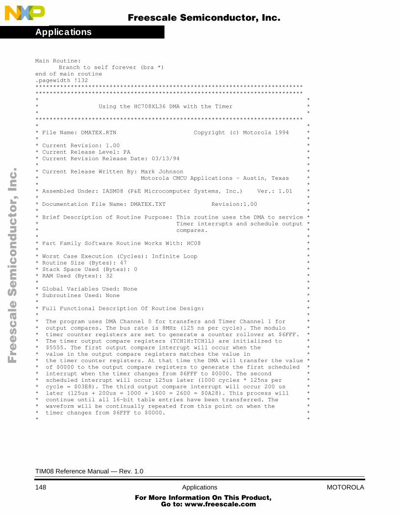
Applications
F
ree
sca
le S
em
ico
nd
uc
tor,
I
Freescale Semiconductor, Inc.n
c..
.
Main Routine:Branch to self forever (bra *)
end of main routine.pagewidth !132********************************************************************************************************************************************************* ** Using the HC708XL36 DMA with the Timer ** ****************************************************************************** ** File Name: DMATEX.RTN Copyright (c) Motorola 1994 ** ** Current Revision: 1.00 ** Current Release Level: PA ** Current Revision Release Date: 03/13/94 ** ** Current Release Written By: Mark Johnson ** Motorola CMCU Applications - Austin, Texas ** ** Assembled Under: IASM08 (P&E Microcomputer Systems, Inc.) Ver.: 1.01 ** ** Documentation File Name: DMATEX.TXT Revision:1.00 ** ** Brief Description of Routine Purpose: This routine uses the DMA to service ** Timer interrupts and schedule output ** compares. ** ** Part Family Software Routine Works With: HC08 ** ** Worst Case Execution (Cycles): Infinite Loop ** Routine Size (Bytes): 47 ** Stack Space Used (Bytes): 0 ** RAM Used (Bytes): 32 ** ** Global Variables Used: None ** Subroutines Used: None ** ** Full Functional Description Of Routine Design: ** ** The program uses DMA Channel 0 for transfers and Timer Channel 1 for ** output compares. The bus rate is 8MHz (125 ns per cycle). The modulo ** timer counter registers are set to generate a counter rollover at $6FFF. ** The timer output compare registers (TCH1H:TCH1L) are initialized to ** $5555. The first output compare interrupt will occur when the ** value in the output compare registers matches the value in ** the timer counter registers. At that time the DMA will transfer the value ** of $0000 to the output compare registers to generate the first scheduled ** interrupt when the timer changes from $6FFF to $0000. The second ** scheduled interrupt will occur 125us later (1000 cycles * 125ns per ** cycle = $03E8). The third output compare interrupt will occur 200 us ** later (125us + 200us = 1000 + 1600 = 2600 = $0A28). This process will ** continue until all 16-bit table entries have been transferred. The ** waveform will be continually repeated from this point on when the ** timer changes from $6FFF to $0000. ** *
TIM08 Reference Manual — Rev. 1.0
148 Applications MOTOROLA For More Information On This Product,
Go to: www.freescale.com

ApplicationsUsing the HC708XL36 DMA with the TIM
F
ree
sca
le S
em
ico
nd
uc
tor,
I
Freescale Semiconductor, Inc.n
c..
.
* System Resource Configuration: ** ** DMA ** 1) Write DMA Source Base Address (D0SH:D0SL = $0060): ** - beginning address for the table of output ** compare values in RAM. ** 2) Write DMA Destination Base Address (D0DH:D0DL = $002A): ** - address of Timer Channel 1 Output Compare Registers ** (TCH1H:TCH1L). ** 3) Configure DMA Channel 0 Control Register (D0C = $89): ** - source/destination address set to increment/static. ** - select word transfers. ** - DMA transfer source set to Timer Channel 1 ** service request. ** 4) Configure DMA Status and Control Register (DSC = $10): ** - enable loop mode for DMA Channel 0. ** 5) Configure DMA Block Length Register (D0DL = $20): ** - number of bytes in RAM table = 32 = $20. ** 6) Configure DMA Control Register 1 (DC1 = 2): ** - enable DMA Channel 0. ** ** Timer ** ** 1) Configure Timer Status and Control Register (TSC = $30): ** - stop and reset Timer. ** 2) Initialize Timer 1 Output Compare Registers (TCH1H:TCH1L): ** - first output compare at $5555. ** 3) Configure Modulo Timer (TMODH:TMODL): ** - counter rollover at $6FFF cycles. ** 4) Configure Timer DMA select (TDMA = 2): ** - DMA service for Timer Channel 1 interrupts. ** 5) Configure Timer Channel 1 Status and Control Reg. (TSC1 = $54): ** - enable output compare interrupts. ** - set up for output compare with toggle ** (* see note below). ** - disable toggle on Timer overflow. ** 6) Configure Timer Status and Control Register (TSC = 0): ** - start Timer. ** - prescaler set to system/1 (default condition). ** ** Note: When the output compare function is enabled, the associated output ** compare pin is set to a logic 1. The first toggle will be a negative ** transition and will occur when the Timer counter reaches $5555. ** ** Main Routine: ** ** Branch to self forever (bra *) ** ** end of main routine ** ** ****************************************************************************** ** Update History: ** Rev: Author: Date: Description of Change: ** ---- ------- ----- ---------------------- ** PA 1.0 Johnson 3/13/94 Original Release ** *****************************************************************************
TIM08 Reference Manual — Rev. 1.0
MOTOROLA Applications 149 For More Information On This Product,
Go to: www.freescale.com

Applications
F
ree
sca
le S
em
ico
nd
uc
tor,
I
Freescale Semiconductor, Inc.n
c..
.
***************************************************************************** ** Motorola reserves the right to make changes without further notice to any ** product herein to improve reliability, function, or design. Motorola does ** not assume any liability arising out of the application or use of any ** product, circuit, or software described herein; neither does it convey any ** license under its patent rights nor the rights of others. Motorola ** products are not designed, intended, or authorized for use as components ** in systems intended for surgical implant into the body, or other ** applications intended to support life, or for any other application in ** which the failure of the Motorola product could create a situation where ** personal injury or death may occur. Should Buyer purchase or use Motorola ** products for any such intended or unauthorized application, Buyer shall ** indemnify and hold Motorola and its officers, employees, subsidiaries, ** affiliates, and distributors harmless against all claims, costs, damages, ** and expenses, and reasonable attorney fees arising out of, directly or ** indirectly, any claim of personal injury or death associated with such ** unintended or unauthorized use, even if such claim alleges that Motorola ** was negligent regarding the design or manufacture of the part. Motorola ** and the Motorola Logo are registered trademarks of Motorola Inc. ** *********************************************************************************************************************************************************$PAGE* ****************************************************************************** ** Part Specific Framework Includes Section ** ** Place the assembler statement ($INCLUDE) to include the part specific ** framework for the target part. ** ******************************************************************************$NOLIST$INCLUDE 'H708XL36.FRK' ;Device specific equates file*$LIST****************************************************************************** ** Equates for Main Routine ** ******************************************************************************Table_start equ $60****************************************************************************** ** RAM Definitions for Main Routine ** ***************************************************************************** org Table_start** Set up table of output compare values in RAM starting at $0060*
TIM08 Reference Manual — Rev. 1.0
150 Applications MOTOROLA For More Information On This Product,
Go to: www.freescale.com
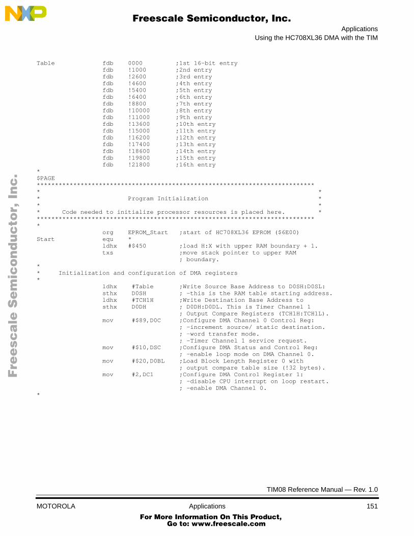
ApplicationsUsing the HC708XL36 DMA with the TIM
F
ree
sca
le S
em
ico
nd
uc
tor,
I
Freescale Semiconductor, Inc.n
c..
.
Table fdb 0000 ;1st 16-bit entry fdb !1000 ;2nd entry fdb !2600 ;3rd entry fdb !4600 ;4th entry fdb !5400 ;5th entry fdb !6400 ;6th entry fdb !8800 ;7th entry fdb !10000 ;8th entry fdb !11000 ;9th entry fdb !13600 ;10th entry fdb !15000 ;11th entry fdb !16200 ;12th entry fdb !17400 ;13th entry fdb !18600 ;14th entry fdb !19800 ;15th entry fdb !21800 ;16th entry*$PAGE***************************************************************************** ** Program Initialization ** ** Code needed to initialize processor resources is placed here. ****************************************************************************** org EPROM_Start ;start of HC708XL36 EPROM ($6E00)Start equ * ldhx #$450 ;load H:X with upper RAM boundary + 1. txs ;move stack pointer to upper RAM ; boundary.** Initialization and configuration of DMA registers* ldhx #Table ;Write Source Base Address to D0SH:D0SL: sthx D0SH ; -this is the RAM table starting address. ldhx #TCH1H ;Write Destination Base Address to sthx D0DH ; D0DH:D0DL. This is Timer Channel 1 ; Output Compare Registers (TCH1H:TCH1L). mov #$89,D0C ;Configure DMA Channel 0 Control Reg: ; -increment source/ static destination. ; -word transfer mode. ; -Timer Channel 1 service request. mov #$10,DSC ;Configure DMA Status and Control Reg: ; -enable loop mode on DMA Channel 0. mov #$20,D0BL ;Load Block Length Register 0 with ; output compare table size (!32 bytes). mov #2,DC1 ;Configure DMA Control Register 1: ; -disable CPU interrupt on loop restart. ; -enable DMA Channel 0.*
TIM08 Reference Manual — Rev. 1.0
MOTOROLA Applications 151 For More Information On This Product,
Go to: www.freescale.com

Applications
F
ree
sca
le S
em
ico
nd
uc
tor,
I
Freescale Semiconductor, Inc.n
c..
.
* Initialization and configuration of Timer registers* mov #$30,TSC ;Stop and reset Timer. ldhx #$5555 ;Initialize output compare regs to sthx TCH1H ; generate first output compare. ldhx #$6FFF ;Configure Modulo Timer: sthx TMODH ; -counter rollover at $6FFF cycles. mov #2,TDMA ;Configure Timer DMA select register: ; -DMA service for Timer Channel 1 ; interrupts. mov #$54,TSC1 ;Configure Timer Channel 1 Status and ; Control Register: ; -enable output compare interrupts. ; -set up for output compare w/ toggle. ; -disable toggle on timer overflow. mov #0,TSC ;Start Timer.***************************************************************************** ** Main Program Loop ** ****************************************************************************** *Main equ * bra * ;stay here forever***************************************************************************** ** Reset Vectors for Main Routine ** ***************************************************************************** org RESET fdb Start
TIM08 Reference Manual — Rev. 1.0
152 Applications MOTOROLA For More Information On This Product,
Go to: www.freescale.com
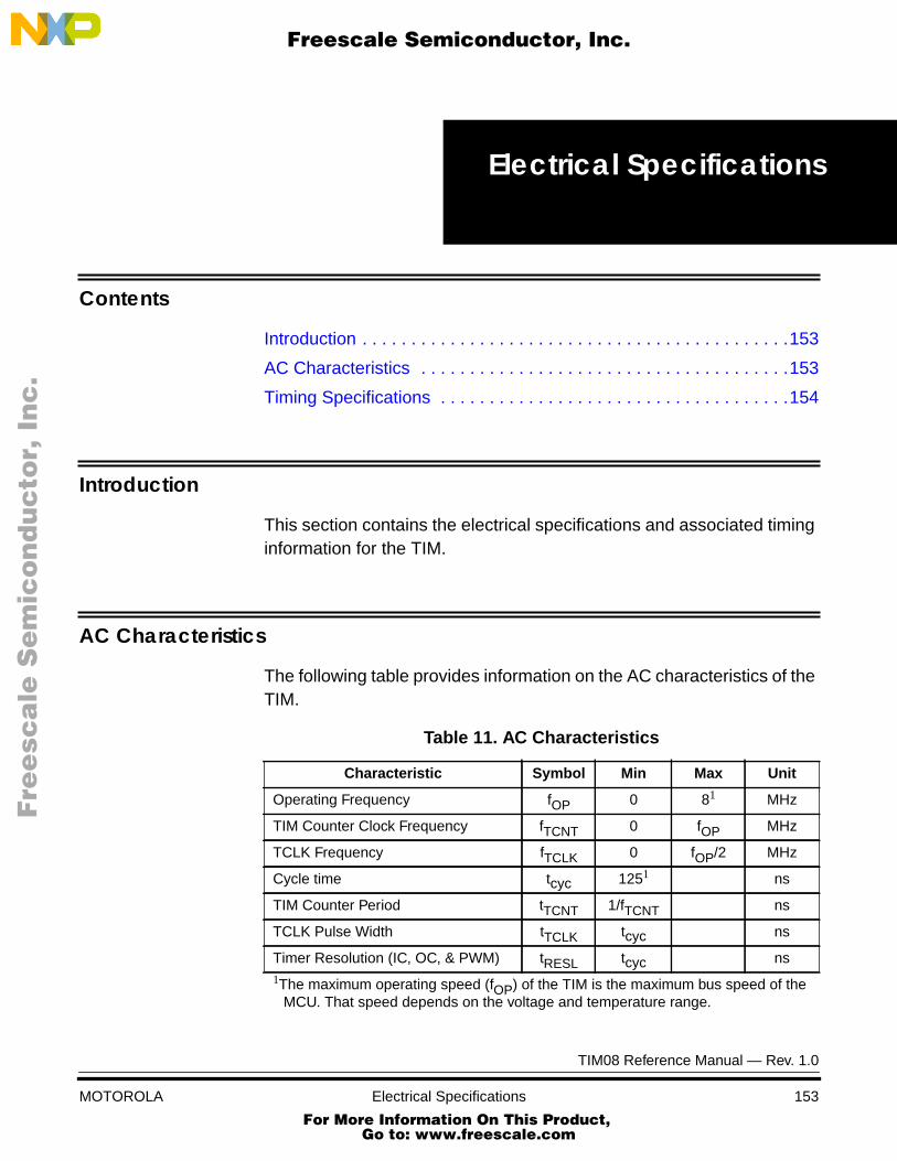
F
ree
sca
le S
em
ico
nd
uc
tor,
IFreescale Semiconductor, Inc.
nc
...
Electrical Specifications
Contents
Introduction . . . . . . . . . . . . . . . . . . . . . . . . . . . . . . . . . . . . . . . . . . . .153
AC Characteristics . . . . . . . . . . . . . . . . . . . . . . . . . . . . . . . . . . . . . .153
Timing Specifications . . . . . . . . . . . . . . . . . . . . . . . . . . . . . . . . . . . .154
Introduction
This section contains the electrical specifications and associated timinginformation for the TIM.
AC Characteristics
The following table provides information on the AC characteristics of theTIM.
Table 11. AC Characteristics
Characteristic Symbol Min Max Unit
Operating Frequency fOP 0 81 MHz
TIM Counter Clock Frequency fTCNT 0 fOP MHz
TCLK Frequency fTCLK 0 fOP/2 MHz
Cycle time tcyc 1251 ns
TIM Counter Period tTCNT 1/fTCNT ns
TCLK Pulse Width tTCLK tcyc ns
Timer Resolution (IC, OC, & PWM) tRESL tcyc ns1The maximum operating speed (fOP) of the TIM is the maximum bus speed of the
MCU. That speed depends on the voltage and temperature range.
TIM08 Reference Manual — Rev. 1.0
MOTOROLA Electrical Specifications 153 For More Information On This Product,
Go to: www.freescale.com

Electrical Specifications
F
ree
sca
le S
em
ico
nd
uc
tor,
I
Freescale Semiconductor, Inc.n
c..
.
Timing Specifications
This section provides information on the timing relationships betweenthe internal bus signals in the MCU. The CPU clock is referenced in theM68HC08 Central Processor Unit Reference Manual, order numberCPU08RM/AD. The bus clocks, IT12 and IT23, are generated by theMCU clock generation module (CGM) and distributed to the MCU bus bythe system integration module (SIM). The SIM also generates theinternal address bus and internal data bus. All TIM timing is referencedto these internal bus signals from the SIM.
The rise/fall timing and hysteresis for the timer channel/port pins isdependent on the port circuit, and is specified in MC68HC708XL36Technical Summary, order number MC68HC708XL36/D.
Figure 55. Internal Bus Signals
CPU CLOCK
INTERNAL
INTERNAL
ADDRESS BUS
DATA BUS
BUS CLOCK: IT12
IT23
T1 T2 T3 T4
1fBUS ns
TIM08 Reference Manual — Rev. 1.0
154 Electrical Specifications MOTOROLA For More Information On This Product,
Go to: www.freescale.com
F
ree
sca
le S
em
ico
nd
uc
tor,
IFreescale Semiconductor, Inc.
nc
...
Memory Map and Registers
Contents
Introduction . . . . . . . . . . . . . . . . . . . . . . . . . . . . . . . . . . . . . . . . . . . .155
Timer Status and Control Register . . . . . . . . . . . . . . . . . . . . . . . . . .156
Timer DMA Select Register . . . . . . . . . . . . . . . . . . . . . . . . . . . . . . .158
Timer Counter Registers . . . . . . . . . . . . . . . . . . . . . . . . . . . . . . . . .160
Timer Counter Modulo Registers . . . . . . . . . . . . . . . . . . . . . . . . . . .161
Timer Channel Status and Control Registers . . . . . . . . . . . . . . . . . .162
Timer Channel Registers . . . . . . . . . . . . . . . . . . . . . . . . . . . . . . . . .168
Introduction
This section contains an overview of the TIM registers. The followingTIM registers are discussed in this section: timer status and controlregister (TSC), timer DMA select register (TDMA), timer counterregisters (TCNTH:TCNTL), timer counter modulo registers(TMODH:TMODL), timer channel status and control registers(TSC0–TSC3), timer channel status and control registers(TSC0–TSC3), and timer channel registers (TCH0H/L–TCH3H/L).
NOTE: The TIM can be implemented with two, four, six or eight channels. Thismanual will show the 4-channel version, as implemented in theMC68HC708XL36.
TIM08 Reference Manual — Rev. 1.0
MOTOROLA Memory Map and Registers 155 For More Information On This Product,
Go to: www.freescale.com

Memory Map and Registers
F
ree
sca
le S
em
ico
nd
uc
tor,
I
Freescale Semiconductor, Inc.n
c..
.
Timer Status and Control Register
Figure 56. Timer Status and Control Register (TSC)
TOF — Timer overflow flag
This clearable flag is set when the timer counter reaches the modulovalue programmed in the timer modulo registers. Clear TOF byreading the timer status and control register when TOF is set and thenwriting a 0 to TOF. If another timer overflow occurs before the clearingsequence is complete, then writing 0 to TOF has no effect. Therefore,a TOF interrupt request cannot be lost due to inadvertent clearing ofTOF. Writing a 1 to this bit has no effect. Reset clears the TOF bit.
1 = Timer counter has reached modulo value.0 = Timer counter has not reached modulo value.
TOE — Timer overflow enable
This read/write bit enables timer overflow interrupts when the TOF bitbecomes set. Reset clears the TOE bit.
1 = Timer overflow interrupts enabled0 = Timer overflow interrupts disabled
TSTOP — Timer stop
This read/write bit stops the timer counter. Counting resumes whenTSTOP is cleared. Reset sets the TSTOP bit, stopping the timercounter until the TIM is enabled.
1 = Timer counter stopped0 = Timer counter active
To preserve the correct timing relationship, TSTOP stops the inputclock to the prescaler. The relationship cannot be preserved whenusing the external TCLK as the timer clock. See Figure 13 for detailson the timing of the TSTOP function.
TSC Bit 7 6 5 4 3 2 1 Bit 0
Read: TOFTOE TSTOP
0 0PS2 PS1 PS0
Write: 0 TRST
Reset: 0 0 1 0 0 0 0 0
TIM08 Reference Manual — Rev. 1.0
156 Memory Map and Registers MOTOROLA For More Information On This Product,
Go to: www.freescale.com

Memory Map and RegistersTimer Status and Control Register
F
ree
sca
le S
em
ico
nd
uc
tor,
I
Freescale Semiconductor, Inc.n
c..
.
NOTE: Do not set the TSTOP bit before entering wait mode if the TIM is requiredto exit wait mode.
TRST — Timer reset
Setting this write-only bit resets the timer counter and the timerprescaler. Setting TRST has no effect on any other registers.Counting resumes from $0000. TRST is cleared automatically afterthe timer counter is reset, and always reads zero. Reset clears theTRST bit.
1 = Prescaler and timer counter cleared0 = No effect
See Figure 14 for details on the timing of the TRST function.
NOTE: Setting the TSTOP and TRST bits simultaneously stops the timercounter at a value of $0000.
Bit 3 — Not used; always reads 0.
PS2–PS0 — Prescaler bits
These read/write bits select the bus clock, one of the six prescaleroutputs, or the TCLK pin as the input to the timer counter. Table 12shows the prescaler selection encoding, including the TIM clocksource, and the function of the TCLK pin. Reset clears the PS2–PS0bits.
Table 12. Prescaler Selection
NOTE: Stop the TIM before changing the prescaler output. Before writing to theprescaler select bits (PS2–PS0), set the timer stop bit (TSTOP).
PS2:PS1:PS0
TIM Clock Source PORT/TCLKFunction
000 Bus Clock PORT
001 Bus Clock ÷ 2 PORT
010 Bus Clock ÷ 4 PORT
011 Bus Clock ÷ 8 PORT
100 Bus Clock ÷ 16 PORT
101 Bus Clock ÷ 32 PORT
110 Bus Clock ÷ 64 PORT
111 TCLK TCLK
TIM08 Reference Manual — Rev. 1.0
MOTOROLA Memory Map and Registers 157 For More Information On This Product,
Go to: www.freescale.com

Memory Map and Registers
F
ree
sca
le S
em
ico
nd
uc
tor,
I
Freescale Semiconductor, Inc.n
c..
.
NOTE: Changing the prescaler control bits while the prescaler is running maycause an extra count if the input clock previously selected was a logiclevel 0 and the new input clock logic level is 1.
See Special Modes for information on stopping the prescaler.
Timer DMA Select Register
NOTE: This register is available only on microcontrollers with a DMA module. Ifno DMA module is included, do not enable the bits described in Figure57. If those bits are enabled, no CPU interrupts for that channel will begenerated or serviced.
The timer DMA register selects either the CPU or the DMA module toservice TIM interrupts. These bits are cleared on reset, selecting theCPU to process interrupts.
Figure 57. Timer DMA Select Register (TDMA)
DMA3S — DMA channel 3 select
This read/write bit enables the DMA to process TIM interrupts ontimer channel 3. Reset clears the DMA3S bit.
1 = Timer channel 3 generates DMA service requests.0 = Timer channel 3 generates CPU interrupt requests.
DMA2S — DMA channel 2 select
This read/write bit enables the DMA to process TIM interrupts ontimer channel 2. Reset clears the DMA2S bit.
1 = Timer channel 2 generates DMA service requests.0 = Timer channel 2 generates CPU interrupt requests.
TDMA Bit 7 6 5 4 3 2 1 Bit 0
Read: 0 0 0 0DMA3S DMA2S DMA1S DMA0S
Write:
Reset: 0 0 0 0 0 0 0 0
TIM08 Reference Manual — Rev. 1.0
158 Memory Map and Registers MOTOROLA For More Information On This Product,
Go to: www.freescale.com

Memory Map and RegistersTimer DMA Select Register
F
ree
sca
le S
em
ico
nd
uc
tor,
I
Freescale Semiconductor, Inc.n
c..
.
DMA1S — DMA channel 1 select
This read/write bit enables the DMA to process TIM interrupts ontimer channel 1. Reset clears the DMA1S bit.
1 = Timer channel 1 generates DMA service requests.0 = Timer channel 1 generates CPU interrupt requests.
DMA0S — DMA channel 0 select
This read/write bit enables the DMA to process TIM interrupts ontimer channel 0. Reset clears the DMA0S bit.
1 = Timer channel 0 generates DMA service requests.0 = Timer channel 0 generates CPU interrupt requests.
TIM08 Reference Manual — Rev. 1.0
MOTOROLA Memory Map and Registers 159 For More Information On This Product,
Go to: www.freescale.com

Memory Map and Registers
F
ree
sca
le S
em
ico
nd
uc
tor,
I
Freescale Semiconductor, Inc.n
c..
.
Timer Counter Registers
These two read-only timer counter registers (TCNT) contain the high andlow bytes of the value in the timer counter. The counter value can beread at any time with user software without affecting its value. Readingthe high byte (TCNTH) latches the contents of the low byte (TCNTL).Subsequent reads of TCNTH do not affect the latched TCNTL value untilTCNTL is read. The LDHX instruction can be used to read a value fromTCNT. The counter is set to $0000 on reset or when the timer reset bit(TRST) is set.
Figure 58. Timer Counter Registers (TCNTH:TCNTL)
TCNTH Bit 7 6 5 4 3 2 1 Bit 0
Read: Bit 15 14 13 12 11 10 9 8
Write:
Reset: 0 0 0 0 0 0 0 0
TCNTL Bit 7 6 5 4 3 2 1 Bit 0
Read: Bit 7 6 5 4 3 2 1 Bit 0
Write:
Reset: 0 0 0 0 0 0 0 0
TIM08 Reference Manual — Rev. 1.0
160 Memory Map and Registers MOTOROLA For More Information On This Product,
Go to: www.freescale.com
Memory Map and RegistersTimer Counter Modulo Registers
F
ree
sca
le S
em
ico
nd
uc
tor,
I
Freescale Semiconductor, Inc.n
c..
.
Timer Counter Modulo Registers
These two read/write timer counter modulo registers (TMOD) contain thehigh and low bytes of the modulo value for the timer counter. When thetimer counter reaches the modulo value, the TOF flag is automaticallyset by hardware, and the timer counter resumes counting from $0000 atthe next clock. The overflow flag (TOF) and overflow interrupts areinhibited after a write to the high byte (TMODH) until the low byte(TMODL) is written. The STHX instruction can be used to write values toTMOD, and the LDHX instruction can be used to read values fromTMOD. Reset sets the timer counter modulo registers to $FFFF,enabling the modulo counter to act as a free-running counter.
Figure 59. Timer Counter Modulo Registers (TMODH:TMODL)
NOTE: If TMODH:TMODL is set to $0000, a TOF is generated on the first cyclein which the match occurs, but not subsequently.
NOTE: Stop and reset the timer counter before writing to the timer countermodulo registers.
TMODH Bit 15 14 13 12 11 10 9 Bit 8
Read:Bit 15 14 13 12 11 10 9 Bit 8
Write:
Reset: 1 1 1 1 1 1 1 1
TMODL Bit 7 6 5 4 3 2 1 Bit 0
Read:Bit 7 6 5 4 3 2 1 Bit 0
Write:
Reset: 1 1 1 1 1 1 1 1
TIM08 Reference Manual — Rev. 1.0
MOTOROLA Memory Map and Registers 161 For More Information On This Product,
Go to: www.freescale.com

Memory Map and Registers
F
ree
sca
le S
em
ico
nd
uc
tor,
I
Freescale Semiconductor, Inc.n
c..
.
Timer Channel Status and Control Registers
The timer channel status and control registers are 8-bit read/writeregisters. These registers are used to configure the timer channel toperform input capture, output compare, or PWM functions. The state ofthese registers is reset to $00.
Each of the timer channel status and control registers does the following:
• Flags input captures and output compares
• Enables input capture and output compare interrupts
• Selects input capture, unbuffered output compare, buffered outputcompare, unbuffered PWM, or buffered PWM operation
• Selects, high, low, or toggling output on output compare or PWMmatch
• Selects rising, falling, or any edge as the active input capturetrigger
• Selects output toggling on timer overflow
• Selects 100% PWM duty cycle
TIM08 Reference Manual — Rev. 1.0
162 Memory Map and Registers MOTOROLA For More Information On This Product,
Go to: www.freescale.com

Memory Map and RegistersTimer Channel Status and Control Registers
F
ree
sca
le S
em
ico
nd
uc
tor,
I
Freescale Semiconductor, Inc.n
c..
.
Figure 60. Timer Channel Statusand Control Registers (TSC0–TSC3)
CHxF— Channel x flag
When channel x is an input capture channel, this clearable bit is setwhen an active edge occurs on the channel x pin. When channel x isan output compare or PWM channel, CHxF is set when the value inthe timer counter registers matches the value in the timer channel xregisters.
When CPU interrupts are enabled (CHxIE:DMAxS = 1:0), clear CHxFby reading the channel x status and control register with CHxF set andthen writing a 0 to CHxF. If another interrupt request occurs before the
TSC0 Bit 7 6 5 4 3 2 1 Bit 0
Read: CH0FCH0IE MS0B MS0A ELS0B ELS0A TOV0 CH0MAX
Write: 0
Reset: 0 0 0 0 0 0 0 0
TSC1 Bit 7 6 5 4 3 2 1 Bit 0
Read: CH1FCH1IE 0 MS1A ELS1B ELS1A TOV1 CH1MAX
Write: 0
Reset: 0 0 0 0 0 0 0 0
TSC2 Bit 7 6 5 4 3 2 1 Bit 0
Read: CH2FCH2IE MS2B MS2A ELS2B ELS2A TOV2 CH2MAX
Write: 0
Reset: 0 0 0 0 0 0 0 0
TSC3 Bit 7 6 5 4 3 2 1 Bit 0
Read: CH3FCH3IE 0 MS3A ELS3B ELS3A TOV3 CH3MAX
Write: 0
Reset: 0 0 0 0 0 0 0 0
TIM08 Reference Manual — Rev. 1.0
MOTOROLA Memory Map and Registers 163 For More Information On This Product,
Go to: www.freescale.com
Memory Map and Registers
F
ree
sca
le S
em
ico
nd
uc
tor,
I
Freescale Semiconductor, Inc.n
c..
.
clearing sequence is complete, then writing zero to CHxF has noeffect. Therefore, an interrupt request cannot be lost due toinadvertent clearing of CHxF.
When DMA service requests are available and enabled(CHxIE:DMAxS = 1:1), clear CHxF by reading or writing to the lowbyte of the channel register (TCHxL). DMA service requests may notbe used with buffered OC/PWM functions.
Writing a 1 to this bit has no effect. Reset clears the CHxF bit.1 = Input capture or OC/PWM match on channel x0 = No input capture or OC/PWM match on channel x
CHxIE — Channel x interrupt enable
This read/write bit enables channel x interrupts. In microcontrollerswith a DMA module, the DMAxS bit in the timer DMA select registerselects channel x CPU interrupts or DMA service requests for theinput capture or unbuffered OC/PWM modes. DMA service requestscannot be used with buffered OC/PWM mode, therefore the DMAxSbit in the timer DMA select register should be cleared to selectchannel x CPU interrupts. Reset clears the CHxIE bit.
1 = Channel x interrupts enabled0 = Channel x interrupts disabled
MSxB — Mode select bit B
MSxB exists only in the channel 0 and channel 2 status and controlregisters, TSC0 and TSC2.
This read/write bit selects buffered OC or buffered PWM operation.Setting MS0B disables the channel 1 status and control register, andreverts TCH1 to general-purpose I/O. Setting MS2B disables thechannel 3 status and control register, and reverts TCH3 togeneral-purpose I/O. Reset clears the MSxB bit.
1 = Buffered OC/PWM mode enabled0 = Buffered OC/PWM mode disabled
TIM08 Reference Manual — Rev. 1.0
164 Memory Map and Registers MOTOROLA For More Information On This Product,
Go to: www.freescale.com
Memory Map and RegistersTimer Channel Status and Control Registers
F
ree
sca
le S
em
ico
nd
uc
tor,
I
Freescale Semiconductor, Inc.n
c..
.
MSxA — Mode select bit A
This bit has different functions, depending on the state of ELSxB andELSxA.
When ELSxB:A = 00, this read/write bit selects the initial output levelof the TCHx pin. To select the level of your initial output, write theappropriate value to MSxA while ELSxB:A = 00. Then configure allbits in the TSCx as required for your application.
1 = Initial output level low0 = Initial output level high
When ELSxB:A ≠ 00, this read/write bit selects input capture mode orunbuffered OC/PWM mode, as shown in Table 13 . MS0A and MS1Aare active only when MS0B = 0. MS2A and MS3A are active onlywhen MS2B = 0. Reset clears the MSxA bit.
1 = Unbuffered OC/PWM operation0 = Input capture operation
NOTE: Stop and reset the TIM before changing a channel function. Beforewriting to the mode select bits (MSxB and MSxA), set the timer stop andtimer reset bits (TSTOP and TRST) in the TSC register.
ELSxB and ELSxA — Edge/level select bits
When channel x is an input capture channel, these read/write bitscontrol the active edge sensing logic on channel x. When channel x isan output compare or PWM channel, ELSxB and ELSxA control thechannel x output behavior when an output compare or pulse widthmatch occurs.
When ELSxB and ELSxA are both clear, channel x is not connectedto the port, and pin TCHx is available as a general-purpose I/O pin.Table 13 shows the configuration selected by ELSxB and ELSxA.Reset clears the ELSxB and ELSxA bits.
TIM08 Reference Manual — Rev. 1.0
MOTOROLA Memory Map and Registers 165 For More Information On This Product,
Go to: www.freescale.com

Memory Map and Registers
F
ree
sca
le S
em
ico
nd
uc
tor,
I
Freescale Semiconductor, Inc.n
c..
.
NOTE: Before enabling the channel register for input capture, make sure thatthe PTE/TCHx pin is stable for a minimum of two bus clocks.
TOVx — Toggle on overflow
When channel x is a buffered or unbuffered OC/PWM channel, thisread/write bit controls the behavior of the channel x output when thetimer counter overflows. When channel x is an input capture channel,TOVx has no effect. Reset clears the TOVx bit.
1 = Channel x pin toggles on timer counter overflow.0 = Channel x pin does not toggle on timer counter overflow.
NOTE: When TOVx is set, a timer counter overflow takes precedence over achannel x output compare if both occur at the same time.
Table 13. Mode, Edge, and Level Selection
MSxB:MSxA
ELSxB:ELSxA Mode Configuration
X0 00 Output Preset Set initial output level high
X1 00 Output Preset Set initial output level low
00 00 Input CaptureTCHx Pin under port control;
set initial output level high
00 01 Input Capture Capture on Rising Edge Only
00 10 Input Capture Capture on Falling Edge Only
00 11 Input Capture Capture on Rising or Falling Edge
01 00 Unbuffered OC/PWMTCHx Pin under port control;
set initial output level low
01 01 Unbuffered OC/PWM Toggle Output on OC/PWM Match
01 10 Unbuffered OC/PWM Clear Output on OC/PWM Match
01 11 Unbuffered OC/PWM Set Output on OC/PWM Match
1X 00 Buffered OC/PWMTCHx Pin under port control;
set initial output level
1X 01 Buffered OC/PWM Toggle Output on OC/PWM Match
1X 10 Buffered OC/PWM Clear Output on OC/PWM Match
1X 11 Buffered OC/PWM Set Output on OC/PWM Match
TIM08 Reference Manual — Rev. 1.0
166 Memory Map and Registers MOTOROLA For More Information On This Product,
Go to: www.freescale.com

Memory Map and RegistersTimer Channel Status and Control Registers
F
ree
sca
le S
em
ico
nd
uc
tor,
I
Freescale Semiconductor, Inc.n
c..
.
CHxMAX — PWM 100% duty cycle
This read/write bit forces the duty cycle of buffered and unbufferedOC/PWM signals to 100%. As Figure 61 shows, the CHxMAX bittakes effect in the cycle after it is set or cleared. The output stays atthe 100% duty cycle level until the cycle after CHxMAX is cleared.CHxMAX affects only the logic level of the channel x pin; outputcompares or pulse width matches can continue to occur and set thechannel x flag. Reset clears the CHxMAX bit.
Figure 61. CHxMAX Latency
OUTPUT COMPARE
TIMER OVERFLOW
TCHx
PERIOD
CHxMAX
TIM08 Reference Manual — Rev. 1.0
MOTOROLA Memory Map and Registers 167 For More Information On This Product,
Go to: www.freescale.com

Memory Map and Registers
F
ree
sca
le S
em
ico
nd
uc
tor,
I
Freescale Semiconductor, Inc.n
c..
.
Timer Channel Registers
These read/write registers are used as the 16-bit input capture registerlatch for input capture functions, and as the 16-bit compare register foroutput compare and PWM functions. For input capture functions, theseregisters latch the value of TCNT when a specified transition is detectedon the corresponding input capture pin. For output compare and PWMfunctions, these registers contain the output compare value for theoutput compare function or the pulse width match value for the PWMfunction. The state of the channel registers after reset is unknown.
In input capture mode (MSxB:MSxA = 0:0), reading the high byte of thechannel register (TCHxH) inhibits input captures until the low byte(TCHxL) is read. This prevents another input capture from overwritingthe TCHxH:TCHxL registers before the previous value has been read.An overwrite of TCHxH:TCHxL will occur if another IC is received beforethe TCHxH is read. The LDHX instruction may be used to read theseregisters.
Writing to the timer channel registers will overwrite any input capturedata.
In unbuffered output compare/PWM modes, output compares/pulsewidth matches are inhibited between writes to TCHxH and TCHxL. Thisprevents another output compare/pulse width match from occurring untilthe new output compare/pulse width value is written. In buffered outputcompare/PWM modes, output compares/pulse width matches areinhibited between writes to TCHxH and TCHxL of the active channel.This prevents another output compare/pulse width match from occurringuntil the new pulse width value is written. Output compares are allowedbetween writes to TCHxH and TCHxL of the inactive channel. The sthxinstruction can be used to write to TCHxH:L.
If a timer channel register is not used for an input capture, outputcompare, or PWM function, it can be used as a storage location.
TIM08 Reference Manual — Rev. 1.0
168 Memory Map and Registers For More Information On This Prod
Go to: www.freescale.com
MOTOROLA
uct,
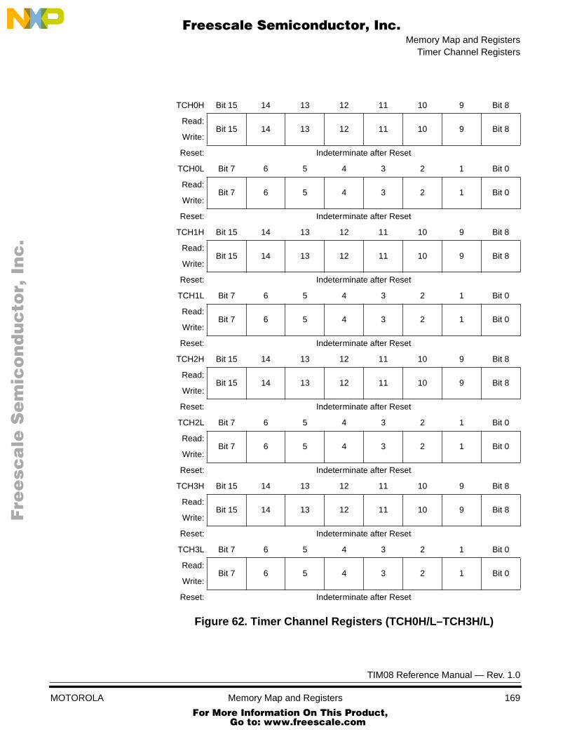
Memory Map and RegistersTimer Channel Registers
F
ree
sca
le S
em
ico
nd
uc
tor,
I
Freescale Semiconductor, Inc.n
c..
.
Figure 62. Timer Channel Registers (TCH0H/L–TCH3H/L)
TCH0H Bit 15 14 13 12 11 10 9 Bit 8
Read:Bit 15 14 13 12 11 10 9 Bit 8
Write:
Reset: Indeterminate after Reset
TCH0L Bit 7 6 5 4 3 2 1 Bit 0
Read:Bit 7 6 5 4 3 2 1 Bit 0
Write:
Reset: Indeterminate after Reset
TCH1H Bit 15 14 13 12 11 10 9 Bit 8
Read:Bit 15 14 13 12 11 10 9 Bit 8
Write:
Reset: Indeterminate after Reset
TCH1L Bit 7 6 5 4 3 2 1 Bit 0
Read:Bit 7 6 5 4 3 2 1 Bit 0
Write:
Reset: Indeterminate after Reset
TCH2H Bit 15 14 13 12 11 10 9 Bit 8
Read:Bit 15 14 13 12 11 10 9 Bit 8
Write:
Reset: Indeterminate after Reset
TCH2L Bit 7 6 5 4 3 2 1 Bit 0
Read:Bit 7 6 5 4 3 2 1 Bit 0
Write:
Reset: Indeterminate after Reset
TCH3H Bit 15 14 13 12 11 10 9 Bit 8
Read:Bit 15 14 13 12 11 10 9 Bit 8
Write:
Reset: Indeterminate after Reset
TCH3L Bit 7 6 5 4 3 2 1 Bit 0
Read:Bit 7 6 5 4 3 2 1 Bit 0
Write:
Reset: Indeterminate after Reset
TIM08 Reference Manual — Rev. 1.0
MOTOROLA Memory Map and Registers 169 For More Information On This Product,
Go to: www.freescale.com
Memory Map and Registers
F
ree
sca
le S
em
ico
nd
uc
tor,
I
Freescale Semiconductor, Inc.n
c..
.
TIM08 Reference Manual — Rev. 1.0
170 Memory Map and Registers For More Information On This Prod
Go to: www.freescale.com
MOTOROLA
uct,

F
ree
sca
le S
em
ico
nd
uc
tor,
IFreescale Semiconductor, Inc.
nc
...
Pin Summary
Contents
Introduction . . . . . . . . . . . . . . . . . . . . . . . . . . . . . . . . . . . . . . . . . . . .171
TIM Pin Functions . . . . . . . . . . . . . . . . . . . . . . . . . . . . . . . . . . . . . . .171
TIM Pin Summary . . . . . . . . . . . . . . . . . . . . . . . . . . . . . . . . . . . . . . .172
Introduction
This section summarizes the TIM pins, the pin configuration control bits,and the data on the external pins.
TIM Pin Functions
The following table summarizes the specific TIM pin functions.
Table 14. Pin Functions
Pin Pin Function
GPI General-purpose input
GPO General-purpose output
ICx TIM input capture
OCx TIM output compare/PWM match
TCLK Pin is used as external clock input.
TIM08 Reference Manual — Rev. 1.0
MOTOROLA Pin Summary 171 For More Information On This Product,
Go to: www.freescale.com

Pin Summary
F
ree
sca
le S
em
ico
nd
uc
tor,
I
Freescale Semiconductor, Inc.n
c..
.
TIM Pin Summary
The following tables summarize the individual TIM pins.
Table 15. TCH0 and TCH2 Pins
Function MSxB:MSxA
ELSxB:ELSxA DDRx Pin
Direction Configuration
GPI 00 00 0 Input PORT Pin
GPO 00 00 1 Output PORT Pin
ICx 00 01 X Input ICx on Rising Edge Only
ICx 00 10 X Input ICx on Falling Edge Only
ICx 00 11 X Input ICx on Rising or Falling Edge
GPI 01 00 0 Input PORT Pin
GPO 01 00 1 Output PORT Pin
OCx 01 01 X Output Toggle Output on OCx
OCx 01 10 X Output Clear Output on OCx
OCx 01 11 X Output Set Output on OCx
GPI 1X 00 0 Input PORT Pin
GPO 1X 00 1 Output PORT Pin
OCx 1X 01 X Output Toggle Output on OCx
OCx 1X 10 X Output Clear Output on OCx
OCx 1X 11 X Output Set Output on OCx
TIM08 Reference Manual — Rev. 1.0
172 Pin Summary For More Information On This Prod
Go to: www.freescale.com
MOTOROLA
uct,

Pin SummaryTIM Pin Summary
F
ree
sca
le S
em
ico
nd
uc
tor,
I
Freescale Semiconductor, Inc.n
c..
.
Table 16. TCH1 and TC H3 Pins
Table 17. TCLK Pin
Function MS0B:MS2B
MS1A:MS3A
ELS1B:ELS1AELS3B:ELS3A
DDREx PinDirection Configuration
GPI 0 0 00 0 Input PORT Pin
GPO 0 0 00 1 Output PORT Pin
ICx 0 0 01 X Input Rising Edge Only
ICx 0 0 10 X Input Falling Edge Only
ICx 0 0 11 X InputRising or Falling
Edge
GPI 0 1 00 0 Input PORT Pin
GPO 0 1 00 1 Output PORT Pin
OCx 0 1 01 X Output Toggle Output
OCx 0 1 10 X Output Clear Output
OCx 0 1 11 X Output Set Output
GPI 1 X XX 0 Input PORT Pin
GPO 1 X XX 1 Output PORT Pin
FunctionPS2:PS1:PS0
DDRE3 Pin Direction Configuration
GPI 0XX 0 Input PORT Pin
GPI X0X 0 Input PORT Pin
GPI XX0 0 Input PORT Pin
GPO 0XX 1 Output PORT Pin
GPO X0X 1 Output PORT Pin
GPO XX0 1 Output PORT Pin
TCLK 111 X Input TIM Clock Input
TIM08 Reference Manual — Rev. 1.0
MOTOROLA Pin Summary 173 For More Information On This Product,
Go to: www.freescale.com
Pin Summary
F
ree
sca
le S
em
ico
nd
uc
tor,
I
Freescale Semiconductor, Inc.n
c..
.
TIM08 Reference Manual — Rev. 1.0
174 Pin Summary For More Information On This Prod
Go to: www.freescale.com
MOTOROLA
uct,

F
ree
sca
le S
em
ico
nd
uc
tor,
IFreescale Semiconductor, Inc.
nc
...
Glossary
$xxxx — The digits following the “$” are in hexadecimal format.
#xxxx — The digits following the “#” indicate an immediate operand.
A — Accumulator. See “accumulator.”
accumulator (A) — An 8-bit general-purpose register in the CPU08.The CPU08 uses the accumulator to hold operands and resultsof arithmetic and nonarithmetic operations.
address bus — The set of signals used to select a specific memorylocation so that the CPU can write information into the memorylocation or read its contents.
addressing mode — The way that the CPU obtains (addresses) theinformation needed to complete an instruction. The M68HC08CPU has 16 addressing modes.
algorithm — A set of specific procedures by which a solution isobtained in a finite number of steps, often used in numericalcalculations.
ALU — Arithmetic logic unit. See “arithmetic logic unit.”
arithmetic logic unit (ALU) — The portion of the CPU of a computerwhere mathematical and logical operations take place. Othercircuitry decodes each instruction and configures the ALU toperform the necessary arithmetic or logical operations at eachstep of an instruction.
assembly language — A method used by programmers forrepresenting machine instructions (binary data) in a moreconvenient form. Each machine instruction is given a simple,short name, called a mnemonic (or memory aid), which has a
TIM08 Reference Manual — Rev. 1.0
MOTOROLA Glossary 175 For More Information On This Product,
Go to: www.freescale.com

Glossary
F
ree
sca
le S
em
ico
nd
uc
tor,
I
Freescale Semiconductor, Inc.n
c..
.
one-to-one correspondence with the machine instruction. Themnemonics are translated into an object code program which amicrocontroller can use.
ASCII — American Standard Code for Information Interchange. Awidely accepted correlation between alphabetic and numericcharacters and specific 7-bit binary numbers.
asynchronous — Refers to circuitry and operations without commonreference signals.
BCD — Binary-coded decimal. See “binary-coded decimal.”
binary — The binary number system using 2 as its base and using onlythe digits 0 and 1. Binary is the numbering system used bycomputers because any quantity can be represented by a seriesof ones and zeros. Electrically, these ones and zeros arerepresented by voltage levels of approximately Vdd (input) andVss (ground), respectively.
binary-coded decimal (BCD) — A notation that uses binary values torepresent decimal quantities. Each BCD digit uses 4 binary bits.Six of the possible 16 binary combinations are considered illegal.
bit — A single binary digit. A bit can hold a single value of zero or one.
Boolean — A mathematical system of representing logic through aseries of algebraic equations that can only be true or false, usingoperators such as AND, OR, and NOT.
branch instructions — Computer instructions that cause the CPU tocontinue processing at a memory location other than the nextsequential address. Most branch instructions are conditional.That is, the CPU will continue to the next sequential address (nobranch) if a condition is false, or continue to some other address(branch) if the condition is true.
buffered — Utilizes a second storage register to prevent overwriting ofvalid data.
bus — A collection of logic signals used to transfer information.
TIM08 Reference Manual — Rev. 1.0
176 Glossary MOTOROLA For More Information On This Product,
Go to: www.freescale.com
Glossary
F
ree
sca
le S
em
ico
nd
uc
tor,
I
Freescale Semiconductor, Inc.n
c..
.
bus clocks — There are two bus clocks, IT12 and IT23. These clocksare generated by the CGM and distributed throughout the MCUby the SIM. The frequency of the bus clocks, or operatingfrequency, is fop. While the frequency of these two clocks is thesame, the phase is different. See Figure 55. Internal BusSignals .
byte — A set of exactly eight binary bits.
C — Abbreviation for carry/borrow in the condition code register of theCPU08. The CPU08 sets the carry/borrow flag when an additionoperation produces a carry out of bit 7 of the accumulator orwhen a subtraction operation requires a borrow. Some logicaloperations and data manipulation instructions also clear or setthe C flag (as in bit test and branch instructions and shifts androtates).
CCR — Abbreviation for condition code register in the CPU08. See“condition code register.”
central processor unit (CPU) — The primary functioning unit of anycomputer system. The CPU controls the execution ofinstructions.
CGM — Clock generation module. See “clock generation module.”
checksum — A value that results from adding a series of binarynumbers. When exchanging information between computers, achecksum gives an indication about the integrity of the datatransfer. If values were transferred incorrectly, it is unlikely thatthe checksum would match the value that was expected.
clear — To establish logic zero state on a bit or bits; the opposite of“set.”
clock — A square wave signal used to sequence events in a computer.
TIM08 Reference Manual — Rev. 1.0
MOTOROLA Glossary 177 For More Information On This Product,
Go to: www.freescale.com

Glossary
F
ree
sca
le S
em
ico
nd
uc
tor,
I
Freescale Semiconductor, Inc.n
c..
.
clock generation module (CGM) — A module in the M68HC08Family. The CGM generates a base clock signal from which thesystem clocks are derived. The CGM may include a crystaloscillator circuit and or phase-locked loop (PLL) circuit.
comparator — A device that compares the magnitude of two inputs. Adigital comparator defines the equality or relative differencesbetween two binary numbers.
condition code register (CCR) — An 8-bit register in the CPU08 thatcontains the interrupt mask bit and five bits (flags) that indicatethe results of the instruction just executed.
control bit — One bit of a register manipulated by software to controlthe operation of the module.
control unit — One of two major units of the CPU. The control unitcontains logic functions that synchronize the machine and directvarious operations. The control unit decodes instructions andgenerates the internal control signals that perform the requestedoperations. The outputs of the control unit drive the executionunit, which contains the arithmetic logic unit (ALU), CPUregisters, and bus interface.
counter clock — The input clock to the TIM counter. This clock is anoutput of the prescaler sub-module. The frequency of thecounter clock is ftcnt, and the period is ttcnt.
CPU — Central processor unit. See “central processor unit.”
CPU08 — The central processor unit of the M68HC08 Family.
CPU cycles — A CPU clock cycle is one period of the internal bus-rateclock, fop, normally derived by dividing a crystal oscillator sourceby two or more so the high and low times will be equal. Thelength of time required to execute an instruction is measured inCPU clock cycles.
TIM08 Reference Manual — Rev. 1.0
178 Glossary MOTOROLA For More Information On This Product,
Go to: www.freescale.com

Glossary
F
ree
sca
le S
em
ico
nd
uc
tor,
I
Freescale Semiconductor, Inc.n
c..
.
CPU registers — Memory locations that are wired directly into the CPUlogic instead of being part of the addressable memory map. TheCPU always has direct access to the information in theseregisters. The CPU registers in an M68HC08 are:
– A (8-bit accumulator)– H:X (16-bit accumulator)– SP (16-bit stack pointer)– PC (16-bit program counter)– CCR (condition code register containing the V, H, I, N, Z,
and C bits)cycles — See “CPU cycles.”
cycle time — The period of the operating frequency: tcyc=1/fop.
data bus — A set of signals used to convey binary information from aCPU to a memory location or from a memory location to a CPU.
data direction register (DDR) — A register which determines thefunction (input or output) of each pin in a data port.
DDR — Data direction register. See “data direction register.”
decimal — Base ten numbering system that uses the digits zerothrough nine.
digital-to-analog converter (DAC) — A particular type of circuitry thatchanges digital information into analog information such asvoltage or current.
direct memory access (DMA) — One of a number of modules thathandle a variety of control functions in the modular M68HC08Family. The DMA can perform interrupt-driven andsoftware-initiated data transfers between any twoCPU-addressable locations. Each DMA channel canindependently transfer data between any addresses in thememory map. DMA transfers reduce CPU overhead required fordata movement interrupts.
direct page — The first 256 bytes of memory ($0000–$00FF); alsocalled page 0.
TIM08 Reference Manual — Rev. 1.0
MOTOROLA Glossary 179 For More Information On This Product,
Go to: www.freescale.com
Glossary
F
ree
sca
le S
em
ico
nd
uc
tor,
I
Freescale Semiconductor, Inc.n
c..
.
DMA — Direct memory access. See “direct memory access.”
duty cycle — A ratio of the amount of time the signal is on versus thetime it is off. It is usually represented by a percentage.
effective address (EA) — The address where an instruction operand islocated. The addressing mode of an instruction determines howthe CPU calculates the effective address of the operand.
EPROM — Erasable, Programmable, Read-Only Memory. Anon-volatile type of memory that can be erased by exposure toan ultraviolet light source.
execution unit (EU) — One of the two major units of the CPUcontaining the arithmetic logic unit (ALU), CPU registers, andbus interface. The outputs of the control unit drive the executionunit.
free-running counter — A device which counts from zero to apre-determined number, then rolls over to zero and beginscounting again.
H — Abbreviation for the upper byte of the 16-bit index register (H:X) inthe CPU08.
H — Abbreviation for “half-carry” in the condition code register of theCPU08. This bit indicates a carry from the low-order four bits ofthe accumulator value to the high-order four bits. The half-carrybit is required for binary-coded decimal arithmetic operations.The decimal adjust accumulator (DAA) instruction uses the stateof the H and C flags to determine the appropriate correctionfactor.
hexadecimal — Base 16 numbering system that uses the digits 0through 9 and the letters A through F. One hexadecimal digit canexactly represent a 4-bit binary value.
high order — The leftmost digit(s) of a number.
H:X — Abbreviation for the 16-bit index register in the CPU08. See“index register.”
TIM08 Reference Manual — Rev. 1.0
180 Glossary MOTOROLA For More Information On This Product,
Go to: www.freescale.com
Glossary
F
ree
sca
le S
em
ico
nd
uc
tor,
I
Freescale Semiconductor, Inc.n
c..
.
I — Abbreviation for “interrupt mask bit” in the condition code register ofthe CPU08. When I is set, all interrupts are disabled. When I iscleared, interrupts are enabled.
index register (H:X) — A 16-bit register in the CPU08. The upper byteof H:X is called H. The lower byte is called X. In the indexedaddressing modes, the CPU uses the contents of H:X todetermine the effective address of the operand. H:X can alsoserve as a temporary data storage location.
input/output (I/O) — Input/output interfaces between a computersystem and the external world. A CPU reads an input to sensethe level of an external signal and writes to an output to changethe level on an external signal.
instructions — Operations that a CPU can perform. Instructions areexpressed by programmers as assembly language mnemonics.A CPU interprets an opcode and its associated operand(s) andinstruction.
instruction set — The instruction set of a CPU is the set of alloperations that the CPU can perform. An instruction set is oftenrepresented with a set of shorthand mnemonics, such as LDA,meaning “load accumulator (A).” Another representation of aninstruction set is with a set of opcodes that are recognized by theCPU.
interrupt — Provide a means to temporarily suspend normal programexecution so that the CPU is freed to service sets of instructionsin response to requests (interrupts) from peripheral devices.Normal program execution can be resumed later from its originalpoint of departure. The CPU08 can process up to 128 separateinterrupt sources, including a software interrupt (SWI).
interrupt service routine — An I/O software routine servicing aspecific interrupt.
I/O — Input/output. See “input/output.”
IRQ — Interrupt request. The overline indicates an active-low signal.
TIM08 Reference Manual — Rev. 1.0
MOTOROLA Glossary 181 For More Information On This Product,
Go to: www.freescale.com

Glossary
F
ree
sca
le S
em
ico
nd
uc
tor,
I
Freescale Semiconductor, Inc.n
c..
.
least significant bit (LSB) — The rightmost digit of a binary value.
logic one — A voltage level approximately equal to the input powervoltage (VDD).
logic zero — A voltage level approximately equal to the ground voltage(VSS).
low order — The rightmost digit(s) of a number.
LS — Least significant.
LSB — Least significant bit. See “least significant bit.”
M68HC08 — A Motorola family of 8-bit MCUs.
machine codes — The binary codes processed by the CPU asinstructions. Machine code includes both opcodes and operanddata.
MCU — Microcontroller unit. See “microcontroller.”
memory location — In the M68HC08 each memory location holds onebyte of data and has a unique address. To store information intoa memory location, the CPU places the address of the locationon the address bus, the data information on the data bus, andasserts the write signal. To read information from a memorylocation, the CPU places the address of the location on theaddress bus and asserts the read signal. In response to the readsignal, the selected memory location places its data onto thedata bus.
memory map — A pictorial representation of all memory locations in acomputer system.
microcontroller — Microcontroller unit (MCU). A complete computersystem, including a CPU, memory, a clock oscillator, andinput/output (I/O) on a single integrated circuit.
TIM08 Reference Manual — Rev. 1.0
182 Glossary MOTOROLA For More Information On This Product,
Go to: www.freescale.com
Glossary
F
ree
sca
le S
em
ico
nd
uc
tor,
I
Freescale Semiconductor, Inc.n
c..
.
mnemonic — Three to five letters that represent a computer operation.For example, the mnemonic form of the “load accumulator”instruction is LDA.
modulo counter — A device capable of being programmed so that itcounts to any number from zero to its maximum possiblemodulus.
most significant bit (MSB) — The leftmost digit of a binary value.
MS — Abbreviation for “most significant.”
MSB — Most significant bit. See “most significant bit.”
multiplexer (mux) — A digital device that can select one of a numberof inputs and pass the logic level of that input on to the output.
N — Abbreviation for “negative,” a bit in the condition code register ofthe CPU08. The CPU sets the negative flag when an arithmeticoperation, logical operation, or data manipulation produces anegative result.
nibble — Half a byte; 4 bits.
object code — The output from an assembler or compiler that is itselfexecutable machine code, or is suitable for processing toproduce executable machine code.
one — A logic high level, a voltage level approximately equal to theinput power voltage (VDD).
one’s complement — An infrequently used form of signed binarynumbers. Negative numbers are simply the complement of theirpositive counterparts. One’s complement is the result of a bit bybit complement of a binary word: all ones are changed to zerosand all zeros changed to ones. One’s complement is two’scomplement without the increment.
opcode — A binary code that instructs the CPU to do a specificoperation in a specific way.
TIM08 Reference Manual — Rev. 1.0
MOTOROLA Glossary 183 For More Information On This Product,
Go to: www.freescale.com
Glossary
F
ree
sca
le S
em
ico
nd
uc
tor,
I
Freescale Semiconductor, Inc.n
c..
.
operand — The fundamental quantity on which a mathematicaloperation is performed. Usually a statement consists of anoperator and an operand. The operator may indicate an addinstruction; the operand therefore will indicate what is to beadded.
oscillator — A circuit that produces a constant frequency square wavethat is used by the computer as a timing and sequencingreference.
overflow — This condition occurs when the modulo counter reaches itsmodulo value and rolls over to zero.
page 0 — The first 256 bytes of memory ($0000–$00FF). Also calleddirect page.
PC — Program counter. See “program counter.”
pointer — Pointer register. An index register is sometimes called apointer register because its contents are used in the calculationof the address of an operand, and therefore “points” to theoperand.
port — A collection of individual I/O signals.
prescaler — A circuit that generates an output signal related to theinput signal by a fractional scale factor such as 1/2, 1/8, 1/10 etc.
program — A set of computer instructions that cause a computer toperform a desired operation or operations.
programming model — The registers of a particular CPU.
program counter (PC) — A 16-bit register in the CPU08. The PCregister holds the address of the next instruction or operand thatthe CPU will use.
TIM08 Reference Manual — Rev. 1.0
184 Glossary MOTOROLA For More Information On This Product,
Go to: www.freescale.com

Glossary
F
ree
sca
le S
em
ico
nd
uc
tor,
I
Freescale Semiconductor, Inc.n
c..
.
pull — The act of reading a value from the stack. In the M68HC08, avalue is pulled by the following sequence of operations. First, thestack pointer register is incremented so that it points to the lastvalue saved on the stack. Next, the value at the addresscontained in the stack pointer register is read into the CPU.
pulse-width — The amount of time a signal is on as opposed to beingin its off state.
pulse-width modulation (PWM) — Controlled variation (modulation)of a pulse width, with a constant frequency.
PWM period — The time required for one complete cycle of a PWMwaveform.
push — The act of storing a value at the address contained in the stackpointer register and then decrementing the stack pointer so thatit points to the next available stack location.
RAM — Random access memory. All RAM locations can be read orwritten by the CPU. The contents of a RAM memory locationremain valid until the CPU writes a different value or until poweris turned off.
RC circuit — A circuit consisting of capacitors and resistors having adefined time constant.
read — To transfer the contents of a memory location to the CPU.
registers — Memory locations wired directly into the CPU logic insteadof being part of the addressable memory map. The CPU alwayshas direct access to the information in these registers. The CPUregisters in an M68HC08 are:
– A (8-bit accumulator)– (H:X) (16-bit accumulator)– SP (16-bit stack pointer)– PC (16-bit program counter)– CCR (condition code register containing the V, H, I, N, Z,
and C bits)
TIM08 Reference Manual — Rev. 1.0
MOTOROLA Glossary 185 For More Information On This Product,
Go to: www.freescale.com
Glossary
F
ree
sca
le S
em
ico
nd
uc
tor,
I
Freescale Semiconductor, Inc.n
c..
.
Memory locations that hold status and control information foron-chip peripherals are called input/output (I/O) and controlregisters.
reset — Reset is used to force a computer system to a known startingpoint and to force on-chip peripherals to known startingconditions.
ROM — Read-only memory. A type of memory that can be read butcannot be changed (written). The contents of ROM must bespecified before manufacturing the MCU.
servo loop — In a servo amplifier, the entire closed loop formed byfeedback from output to input. In a position servo, the outputposition is compared to a command signal at the input.
set — To establish a logic one state on a bit or bits; opposite of “clear.”
signal groups — Groups of electronic signals related by function.
signed — A form of binary number representation accommodating bothpositive and negative numbers. The most significant bit is usedto indicate whether the number is positive or negative, normallyzero for positive and one for negative, and the other seven bitsindicate the magnitude.
SIM — System integration module. See “system integration module.”
software interrupt (SWI) — An instruction that will cause an interruptand its associated vector fetch.
SP — Stack pointer. See “stack pointer.”
stack — A mechanism for temporarily saving CPU register valuesduring interrupts and subroutines. The CPU maintains thisstructure with the stack pointer (SP) register, which contains theaddress of the next available (empty) storage location on thestack. When a subroutine is called, the CPU pushes (stores) thelow-order and high-order bytes of the return address on thestack before starting the subroutine instructions. When thesubroutine is done, a return from subroutine (RTS) instruction
TIM08 Reference Manual — Rev. 1.0
186 Glossary MOTOROLA For More Information On This Product,
Go to: www.freescale.com

Glossary
F
ree
sca
le S
em
ico
nd
uc
tor,
I
Freescale Semiconductor, Inc.n
c..
.
causes the CPU to recover the return address from the stackand continue processing where it left off before the subroutine.Interrupts work in the same way except that all CPU registers aresaved on the stack instead of just the program counter. The Hregister is not pushed on the stack during an interrupt.
stack pointer (SP) — A 16-bit register in the CPU08 containing theaddress of the next available (empty) storage on the stack.
status bit — One bit of a register used to store information about thestatus of the module.
subroutine — A sequence of instructions to be used more than once inthe course of a program. The last instruction in a subroutine is areturn from subroutine (RTS) instruction. At each place in themain program where the subroutine instructions are needed, ajump or branch to subroutine (JSR or BSR) instruction is used tocall the subroutine. The CPU leaves the flow of the mainprogram to execute the instructions in the subroutine. When theRTS instruction is executed, the CPU returns to the mainprogram where it left off.
SWI — Software interrupt. See “software interrupt.”
synchronous — Refers to two or more things made to happensimultaneously in a system by means of a common referencesignal.
system integration module (SIM) — One of a number of modules thathandle a variety of control functions in the modular M68HC08Family. The SIM controls mode of operation, resets andinterrupts, and system clock generation.
TIM — Timer Interface Module.
timer — A module used to relate events in a system to a point in time.
toggle — To change the state of an output from a logic zero to a logicone or from a logic one to a logic zero.
TIM08 Reference Manual — Rev. 1.0
MOTOROLA Glossary 187 For More Information On This Product,
Go to: www.freescale.com

Glossary
F
ree
sca
le S
em
ico
nd
uc
tor,
I
Freescale Semiconductor, Inc.n
c..
.
two’s complement — A means of performing binary subtraction usingaddition techniques. The most significant bit of a two’scomplement number indicates the sign of the number (1indicates negative). The two’s complement negative of a numberis obtained by inverting each bit in the number and then adding 1to the result.
unbuffered — Utilizes only one register for data; new data overwritescurrent data.
unsigned — Refers to a binary number representation in which allnumbers are assumed positive. With signed binary, the mostsignificant bit is used to indicate whether the number is positiveor negative, normally zero for positive and one for negative, andthe other seven bits indicating the magnitude.
variable — A value that changes during the course of executing aprogram.
waveform — A graphical representation in which the amplitude of awave is plotted against time.
word — Two bytes or 16 bits, treated as a unit.
write — The transfer of a byte of data from the CPU to a memorylocation.
X — Abbreviation for the lower byte of the index register (H:X) in theCPU08.
Z — Abbreviation for zero, a bit in the condition code register of theCPU08. The CPU08 sets the zero flag when an arithmeticoperation, logical operation, or data manipulation produces aresult of $00.
zero — A logic low level, a voltage level approximately equal to theground voltage (Vss).
TIM08 Reference Manual — Rev. 1.0
188 Glossary MOTOROLA For More Information On This Product,
Go to: www.freescale.com

F
ree
sca
le S
em
ico
nd
uc
tor,
IFreescale Semiconductor, Inc.
nc
...
Index
AAC characteristics .............................................................................153
Applicationsgeneral TIM08 information ..........................................................121input capture ...............................................................................121output compare ...........................................................................123PWM ...........................................................................................125PWM controlled RC digital to analog converter ..........................131Servo loop motor control .............................................................139using the HC708XL36 DMA with the TIM08 ...............................144
Auxiliary Timer Clock Input (PTE3/TCLK) ..........................................38
BBuffered output compare
diagram .........................................................................................74functions ........................................................................................72mode and level selection ...............................................................77
Buffered PWMdiagram .........................................................................................93functions ........................................................................................90mode and level selection ...............................................................96
CCapture/compare unit
buffered compare functions ...........................................................72buffered output compare mode and level selection ......................77buffered pulse width modulation functions ....................................90input capture functions ..................................................................57input capture mode and edge selection ........................................62input capture timing diagram .........................................................58
TIM08 Reference Manual — Rev. 1.0
MOTOROLA Index 189 For More Information On This Product,
Go to: www.freescale.com

Index
F
ree
sca
le S
em
ico
nd
uc
tor,
I
Freescale Semiconductor, Inc.n
c..
.
timer channel and control registers ...............................................75timer channel registers ................................................63, 70, 71, 78timer channel status and control registers ......60, 67, 75, 83, 84, 94unbuffered output compare functions ............................................65unbuffered output compare mode and level selection ..................70unbuffered output compare timing diagram ..................................66unbuffered pulse width modulation functions ................................80
CHxMAX latency ................................................................................97
CPU interrupts ..................................................................................104
DDMA service requests ......................................................................111
EEdge selection and input capture mode .............................................62
Electrical specificationAC characteristics .......................................................................153internal bus signals .....................................................................154timing specifications ....................................................................154
GGeneral purpose I/O
description .....................................................................................37
II/O .......................................................................................................37
IC ........................................................................................................57
Input capturedescription ...................................................................................121functions ........................................................................................57mode and edge selection ..............................................................62pins ................................................................................................37timing ...................................................................................105, 111timing diagram ...............................................................................58
TIM08 Reference Manual — Rev. 1.0
190 Index MOTOROLA For More Information On This Product,
Go to: www.freescale.com

Index
F
ree
sca
le S
em
ico
nd
uc
tor,
I
Freescale Semiconductor, Inc.n
c..
.
Input capture/output compare pins .....................................................36
Internal bus signals ...........................................................................154
InterruptsCPU interrupts .............................................................................104input capture timing .............................................................105, 111output compare/PWM timing ...............................................109, 113TIM interrupt priority ....................................................................104timer DMA select register (TDMA) ..............................................102timer overflow timing ...................................................................105
LLDHX ..................................................................................................54
MMemory map and registers
timer channel registers ................................................................168timer channel status and control registers ..................................162timer counter modulo registers ....................................................161timer counter registers ................................................................160timer DMA select register (TDMA) ..............................................158timer status and control register (TSC) .......................................156
Modulo countersimplified block diagram ................................................................48timer counter .................................................................................47timer counter modulo registers ......................................................54timer counter registers ..................................................................53TRST timing ..................................................................................52TSTOP timing ................................................................................50
Monitor mode ....................................................................................117
OOutput compare ................................................................................123
Output compare pins ..........................................................................37
Output compare/input capture pins ....................................................36
TIM08 Reference Manual — Rev. 1.0
MOTOROLA Index 191 For More Information On This Product,
Go to: www.freescale.com

Index
F
ree
sca
le S
em
ico
nd
uc
tor,
I
Freescale Semiconductor, Inc.n
c..
.
Output compare/PWM timing ...........................................................109
Output comparesbuffered .........................................................................................28unbuffered .....................................................................................28
PPin functions .....................................................................................171
Pin summaryTCH0 ...........................................................................................172TCH1 ...........................................................................................173TCH2 ...........................................................................................172TCH3 ...........................................................................................173TCLK ...........................................................................................173TIM pin functions .................................................................171, 172
Pins .....................................................................................................37
PrescalerTCLK timing ..................................................................................41timer status and control register (TSC) .........................................41TRST timing ..................................................................................44TSTOP timing ................................................................................42
PTE3/TCLK ........................................................................................38
Pulse width modulation .......................................................................30
PWMapplication ...................................................................................125block diagram ................................................................................31buffered signal generation .............................................................33controlled RC digital to analog converter ....................................131output pins .....................................................................................37period and pulse width ............................................................80, 90unbuffered functions ......................................................................80unbuffered signal generation .........................................................32
PWM signal generationbuffered .........................................................................................33unbuffered .....................................................................................32
TIM08 Reference Manual — Rev. 1.0
192 Index For More Information On This Prod
Go to: www.freescale.com
MOTOROLA
uct,

Index
F
ree
sca
le S
em
ico
nd
uc
tor,
I
Freescale Semiconductor, Inc.n
c..
.
RRegisters
overview ......................................................................................155TSCx .............................................................................................37
SService requests
DMA ............................................................................................111
Servo loop motor control ..................................................................139
Signal descriptionsintroduction ....................................................................................35signal groups .................................................................................36
Special modesmonitor mode ..............................................................................117stop mode ...................................................................................116wait mode ....................................................................................116
STHX ..................................................................................................54
Stop mode ........................................................................................116
TTCH0 ................................................................................................172
TCH0H/L-TCH3H/L ..........................................................63, 64, 70, 78
TCH1 ................................................................................................173
TCH2 ................................................................................................172
TCH3 ................................................................................................173
TCHxH L .............................................................................................59
TCHxH TCHxL ....................................................................................37
TCHxH/L .............................................................................................57
TCHxL ................................................................................................61
TCLK ................................................................................................173
TCNT ......................................................................................47, 48, 53
TCNTH ...............................................................................................53
TCNTH TCNTL ...................................................................................20
TIM08 Reference Manual — Rev. 1.0
MOTOROLA Index 193 For More Information On This Product,
Go to: www.freescale.com
Index
F
ree
sca
le S
em
ico
nd
uc
tor,
I
Freescale Semiconductor, Inc.n
c..
.
TCNTL ................................................................................................53
TDMA .......................................................................................102, 158
TIM interrupt priority .........................................................................104
TIM pin functions ..............................................................................171
TIM08block diagram ................................................................................22buffered output compare simplified block diagram ........................29buffered output compares .............................................................28buffered PWM signal generation ...................................................33buffered PWM simplified block diagram ........................................34features .........................................................................................24input capture concepts ..................................................................25input capture simplified block diagram ..........................................25output compare concepts ..............................................................26output compare simplified block diagram ......................................27pulse-width modulation block diagram ..........................................31pulse-width modulation concepts ..................................................30PWM .............................................................................................30PWM block diagram ......................................................................31submodules ...................................................................................20unbuffered output compares .........................................................28unbuffered PWM signal generation ...............................................32
Timer channel registers (TCH0H/L-TCH3H/L)buffered OC ...................................................................................78description .............................................................................63, 168unbuffered OC ...............................................................................70
Timer channel status and control registers TSC0-TSC3buffered OC ...................................................................................75buffered PWM ...............................................................................94description .............................................................................60, 162unbuffered OC ...............................................................................67unbuffered PWM ...........................................................................83
Timer counter .....................................................................................47
Timer counter modulo registers ..................................................54, 161
Timer counter registers ...............................................................53, 160
Timer DMA select register ................................................................102
TIM08 Reference Manual — Rev. 1.0
194 Index For More Information On This Prod
Go to: www.freescale.com
MOTOROLA
uct,

Index
F
ree
sca
le S
em
ico
nd
uc
tor,
I
Freescale Semiconductor, Inc.n
c..
.
Timer DMA select register (TDMA) ..................................................158
Timer overflow timing .......................................................................105
Timer status and control register (TSC) ...............................41, 49, 156
Timing specifications ........................................................................154
TMOD ...........................................................................................48, 54
TMODH ..............................................................................................54
TMODH TMODL ...........................................................................20, 54
TMODL ...............................................................................................54
TOF ........................................................................................48, 49, 54
TRST ............................................................................................44, 51
TRST timing ........................................................................................52
TSC ................................................................................40, 41, 49, 156
TSC0 ..................................................................................................75
TSC0-TSC2 ........................................................................................94
TSC0-TSC3 ............................................................................60, 67, 83
TSC2 ..................................................................................................75
TSCx .............................................................................................37, 57
TSTOP ................................................................................................49
TSTOP timing ...............................................................................42, 50
UUnbuffered output compare functions ................................................65
Unbuffered output compare timing diagram .......................................66
Unbuffered PWM functions .................................................................80
Unbuffered PWM mode and level selection .......................................86
Unbuffered PWM timing diagram .......................................................82
Using the HC708XL36 DMA with the TIM08 ....................................144
WWait mode ........................................................................................116
TIM08 Reference Manual — Rev. 1.0
MOTOROLA Index 195 For More Information On This Product,
Go to: www.freescale.com

Index
F
ree
sca
le S
em
ico
nd
uc
tor,
I
Freescale Semiconductor, Inc.n
c..
.
TIM08 Reference Manual — Rev. 1.0
196 Index For More Information On This Prod
Go to: www.freescale.com
MOTOROLA
uct,

F
ree
sca
le S
em
ico
nd
uc
tor,
I
Freescale Semiconductor, Inc.n
c..
.
For More Information On This Product,
Go to: www.freescale.com

F
ree
sca
le S
em
ico
nd
uc
tor,
I
Freescale Semiconductor, Inc.n
c..
.
TIM08RM/AD
How to reach us:USA/EUROPE/Locations Not Listed: Motorola Literature Distribution; P.O. Box 20912; Phoenix, Arizona 85036.1-800-441-2447 or
602-303-5454MFAX: [email protected] – TOUCHTONE 602-244-6609INTERNET: http://Design-NET.comJAPAN: Nippon Motorola Ltd.; Tatsumi-SPD-JLDC, 6F Seibu-Butsuryu-Center, 3-14-2 Tatsumi Koto-Ku, Tokyo 135, Japan.
03-81-3521-8315ASIA/PACIFIC: Motorola Semiconductors H.K. Ltd.; 8B Tai Ping Industrial Park, 51 Ting Kok Road, Tai Po, N.T., Hong Kong. 852-26629298
For More Information On This Product, Go to: www.freescale.com