TI reference design number: PMP9367 Rev A1 Input: 6-40V ...
21
Created on: 4/5/2014 PMP9367 Rev A1 Test Results Page 1 of 20 Power Management Solutions TI reference design number: PMP9367 Rev A1 Input: 6-40V Nominal 12V Output: 5V @ 3.5A (USB CH 1: 5V @ 1A) (USB CH 2: 5V @ 2.1A) DC–DC Converter Test Results
Transcript of TI reference design number: PMP9367 Rev A1 Input: 6-40V ...

Created on: 4/5/2014
PMP9367 Rev A1 Test Results
Page 1 of 20 Power Management Solutions
TI reference design number: PMP9367 Rev A1
Input: 6-40V
Nominal 12V
Output: 5V @ 3.5A
(USB CH 1: 5V @ 1A)
(USB CH 2: 5V @ 2.1A)
DC–DC Converter Test Results

Created on: 4/5/2014
PMP9367 Rev A1 Test Results
Page 2 of 20 Power Management Solutions
Table of Contents 1. Circuit Description ....................................................................................................... 3 2. Fabrication .................................................................................................................. 3
2.1 Block Diagram ....................................................................................................... 5 3. Efficiency ..................................................................................................................... 6 4. Load Regulation .......................................................................................................... 6 5. Thermal ....................................................................................................................... 8
Top View ...................................................................................................................... 8
6. Power Up USB CH1 ................................................................................................... 9 6.1 Power Up at 6V Input – No Load Power Up at 6V Input –1A Load ..................... 9 6.2 Power Up at 12V Input – No Load Power Up at 12V Input –1A Load ................. 9
6.3 Power Up at 36V Input – No Load Power Up at 36V Input –1A Load ............... 10 Power Up USB CH2 ...................................................................................................... 11
6.4 Power Up at 6V Input – No Load Power Up at 6V Input –2.1A Load ................ 11
6.5 Power Up at 12V Input – No Load Power Up at 12V Input –2.1A Load ............ 11 6.6 Power Up at 36V Input – No Load Power Up at 12V Input –2.1A Load ............ 12
7. Switching and Ripple ................................................................................................ 13
7.1 LM3150 5VOUT @ 3.1A ................................................................................ 13 8. Transient Response ................................................................................................. 14
8.1 12V Input – 0.5A to 1A Step, 100mA/µs, 100 Hz. USB Ch1 .............................. 14 8.2 12V Input – 1.05A to 2.1A Step, 100mA/µs, 100 Hz. USB Ch2 ........................... 14
9. Current Limit Tests 12V Input .................................................................................... 15
9.1 LM3150 ........................................................................................................... 15 -12Vin - No Load -12Vin - 3.5A Load ................................................................ 15
9.2 USB CH1 ........................................................................................................ 15 -12Vin - No Load -12Vin - 1A Load ................................................................... 15
9.3 USB CH2 ........................................................................................................ 16 -12V in - No Load -12Vin - 2.1A Load ................................................................ 16
10.1 Short Circuit Tests ................................................................................................. 17 10.1 12Vin, LM3150 No Load 12Vin, LM3150 3.1A Load .............................. 17 10.2 12Vin, USB CH1 No Load 12Vin, USB CH1 1A Load ............................... 17 10.3 12Vin, USB CH2 No Load 12Vin, USB CH2 2.1A Load ............................ 18
11. Short Circuit Recovery Tests ................................................................................... 19 11.1 12Vin, LM3150 No Load 12Vin, LM3150 3.1A Load ................................ 19 11.2 12Vin, USB CH1 No Load 12Vin, USB CH1 1A Load ............................... 19 11.3 12Vin, USB CH2 No Load 12Vin, USB CH2 2.1A Load ............................. 20

Created on: 4/5/2014
PMP9367 Rev A1 Test Results
Page 3 of 20 Power Management Solutions
1. Circuit Description PMP9367 is a dual USB car charger. This design utilizes the LM3150, TPS2561 Dual Channel
Power Switch and a TPS2513 USB Dedicated Charging Port Controller. This design operates
from 6 to 40V in. The outputs is set to 5V, channel one has a 1A current limit and channel two
has a 2.1A current limit. This design has a switching frequency of 300 kHz.
2. Fabrication
The PMP9367 is a four layer board with overall dimensions of 0.713” (18mm) x 2.2” (55mm).
The copper weight is 1oz on the outer layers and 0.5oz the inner layers.
Top Layer
USB Direct Charging Port

Created on: 4/5/2014
PMP9367 Rev A1 Test Results
Page 4 of 20 Power Management Solutions
Bottom Layer
USB Direct Charging Port

Created on: 4/5/2014
PMP9367 Rev A1 Test Results
Page 5 of 20 Power Management Solutions
2.1 Block Diagram

Created on: 4/5/2014
PMP9367 Rev A1 Test Results
Page 6 of 20 Power Management Solutions
3. Efficiency
4. Load Regulation
70%
75%
80%
85%
90%
95%
100%
0 2 4 6 8 10 12 14 16 18
Effi
cie
ncy
Power Out (W)
PMP9367 6V 12V 24V
4.934.944.954.964.974.984.99
55.015.025.035.04
0 0.2 0.4 0.6 0.8 1 1.2
VO
UT
(V)
Iout (A)
Ch1 VOUT1

Created on: 4/5/2014
PMP9367 Rev A1 Test Results
Page 7 of 20 Power Management Solutions
4.86
4.88
4.9
4.92
4.94
4.96
4.98
5
5.02
5.04
0 0.5 1 1.5 2 2.5
VO
UT
(V)
IOUT (A)
CH2 VOUT2
Created on: 4/5/2014
PMP9367 Rev A1 Test Results
Page 8 of 20 Power Management Solutions
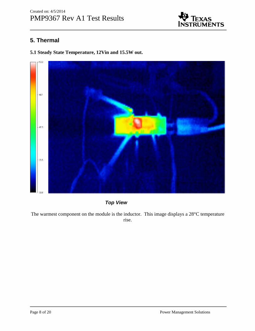
5. Thermal
5.1 Steady State Temperature, 12Vin and 15.5W out.
Top View
The warmest component on the module is the inductor. This image displays a 28°C temperature
rise.

Created on: 4/5/2014
PMP9367 Rev A1 Test Results
Page 9 of 20 Power Management Solutions
6. Power Up USB CH1 6.1 Power Up at 6V Input – No Load Power Up at 6V Input –1A Load
Channel 1 VIN
Channel 2 5Vout LM3150
Channel 3 J1 5Vout
Channel 4 IIN
6.2 Power Up at 12V Input – No Load Power Up at 12V Input –1A Load
Channel 1 VIN
Channel 2 5Vout LM3150
Channel 3 J1 5Vout
Channel 4 IIN
Created on: 4/5/2014
PMP9367 Rev A1 Test Results
Page 10 of 20 Power Management Solutions
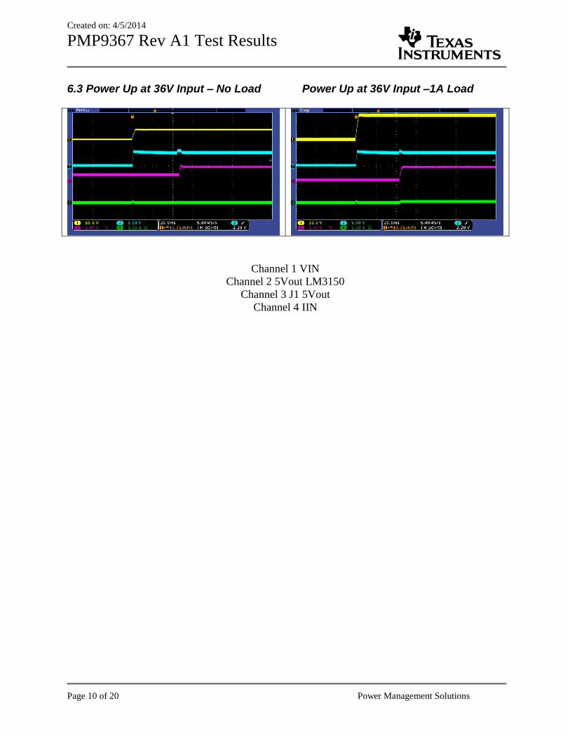
6.3 Power Up at 36V Input – No Load Power Up at 36V Input –1A Load
Channel 1 VIN
Channel 2 5Vout LM3150
Channel 3 J1 5Vout
Channel 4 IIN

Created on: 4/5/2014
PMP9367 Rev A1 Test Results
Page 11 of 20 Power Management Solutions
Power Up USB CH2 6.4 Power Up at 6V Input – No Load Power Up at 6V Input –2.1A Load
Channel 1 VIN
Channel 2 5Vout LM3150
Channel 3 J2 5Vout
Channel 4 IIN
6.5 Power Up at 12V Input – No Load Power Up at 12V Input –2.1A Load
Channel 1 VIN
Channel 2 5Vout LM3150
Channel 3 J2 5Vout
Channel 4 IIN

Created on: 4/5/2014
PMP9367 Rev A1 Test Results
Page 12 of 20 Power Management Solutions
6.6 Power Up at 36V Input – No Load Power Up at 12V Input –2.1A Load
Channel 1 VIN
Channel 2 5Vout LM3150
Channel 3 J2 5Vout
Channel 4 IIN

Created on: 4/5/2014
PMP9367 Rev A1 Test Results
Page 13 of 20 Power Management Solutions
7. Switching and Ripple 7.1 LM3150 5VOUT @ 3.1A
The cursors indicate 7mV ripple.
Channel 1 VSW
Channel 2 5Vout

Created on: 4/5/2014
PMP9367 Rev A1 Test Results
Page 14 of 20 Power Management Solutions
8. Transient Response
A load step was applied to each channel and the transient response of the controller was monitored.
8.1 12V Input – 0.5A to 1A Step, 100mA/µs, 100 Hz. USB Ch1
Cursors indicate ~5mV deviation across output capacitor.
8.2 12V Input – 1.05A to 2.1A Step, 100mA/µs, 100 Hz. USB Ch2
Cursors indicate ~10mV deviation across output capacitor.
Created on: 4/5/2014
PMP9367 Rev A1 Test Results
Page 15 of 20 Power Management Solutions
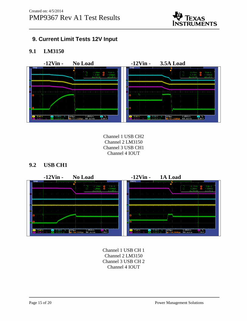
9. Current Limit Tests 12V Input
9.1 LM3150
-12Vin - No Load -12Vin - 3.5A Load
Channel 1 USB CH2
Channel 2 LM3150
Channel 3 USB CH1
Channel 4 IOUT
9.2 USB CH1
-12Vin - No Load -12Vin - 1A Load
Channel 1 USB CH 1
Channel 2 LM3150
Channel 3 USB CH 2
Channel 4 IOUT
Created on: 4/5/2014
PMP9367 Rev A1 Test Results
Page 16 of 20 Power Management Solutions
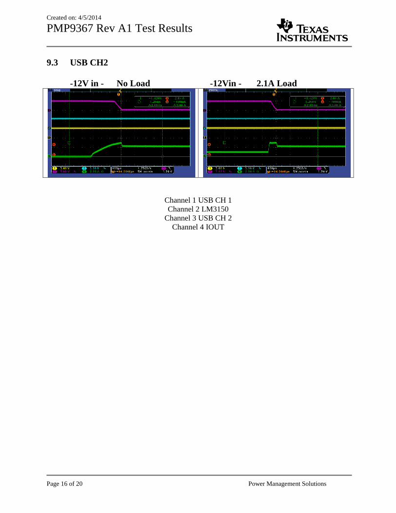
9.3 USB CH2
-12V in - No Load -12Vin - 2.1A Load
Channel 1 USB CH 1
Channel 2 LM3150
Channel 3 USB CH 2
Channel 4 IOUT

Created on: 4/5/2014
PMP9367 Rev A1 Test Results
Page 17 of 20 Power Management Solutions
10.1 Short Circuit Tests
10.1 12Vin, LM3150 No Load 12Vin, LM3150 3.1A Load
Channel 1 USB CH 1
Channel 2 LM3150
Channel 3 USB CH 2
Channel 4 IOUT
10.2 12Vin, USB CH1 No Load 12Vin, USB CH1 1A Load
Channel 1 USB CH 1
Channel 2 LM3150
Channel 3 USB CH 2
Channel 4 IOUT

Created on: 4/5/2014
PMP9367 Rev A1 Test Results
Page 18 of 20 Power Management Solutions
10.3 12Vin, USB CH2 No Load 12Vin, USB CH2 2.1A Load
Channel 1 USB CH 1
Channel 2 LM3150
Channel 3 USB CH 2
Channel 4 IOUT

Created on: 4/5/2014
PMP9367 Rev A1 Test Results
Page 19 of 20 Power Management Solutions
11. Short Circuit Recovery Tests
11.1 12Vin, LM3150 No Load 12Vin, LM3150 3.1A Load
Channel 3 VOUT
Channel 4 IOUT
11.2 12Vin, USB CH1 No Load 12Vin, USB CH1 1A Load
Channel 3 VOUT
Channel 4 IOUT

Created on: 4/5/2014
PMP9367 Rev A1 Test Results
Page 20 of 20 Power Management Solutions
11.3 12Vin, USB CH2 No Load 12Vin, USB CH2 2.1A Load
Channel 3 VOUT
Channel 4 IOUT

IMPORTANT NOTICE AND DISCLAIMERTI PROVIDES TECHNICAL AND RELIABILITY DATA (INCLUDING DATASHEETS), DESIGN RESOURCES (INCLUDING REFERENCEDESIGNS), APPLICATION OR OTHER DESIGN ADVICE, WEB TOOLS, SAFETY INFORMATION, AND OTHER RESOURCES “AS IS”AND WITH ALL FAULTS, AND DISCLAIMS ALL WARRANTIES, EXPRESS AND IMPLIED, INCLUDING WITHOUT LIMITATION ANYIMPLIED WARRANTIES OF MERCHANTABILITY, FITNESS FOR A PARTICULAR PURPOSE OR NON-INFRINGEMENT OF THIRDPARTY INTELLECTUAL PROPERTY RIGHTS.These resources are intended for skilled developers designing with TI products. You are solely responsible for (1) selecting the appropriateTI products for your application, (2) designing, validating and testing your application, and (3) ensuring your application meets applicablestandards, and any other safety, security, or other requirements. These resources are subject to change without notice. TI grants youpermission to use these resources only for development of an application that uses the TI products described in the resource. Otherreproduction and display of these resources is prohibited. No license is granted to any other TI intellectual property right or to any third partyintellectual property right. TI disclaims responsibility for, and you will fully indemnify TI and its representatives against, any claims, damages,costs, losses, and liabilities arising out of your use of these resources.TI’s products are provided subject to TI’s Terms of Sale (https:www.ti.com/legal/termsofsale.html) or other applicable terms available eitheron ti.com or provided in conjunction with such TI products. TI’s provision of these resources does not expand or otherwise alter TI’sapplicable warranties or warranty disclaimers for TI products.IMPORTANT NOTICE
Mailing Address: Texas Instruments, Post Office Box 655303, Dallas, Texas 75265Copyright © 2021, Texas Instruments Incorporated
![Fonte estabilizada [0-40V x 5A].pdf](https://static.fdocuments.net/doc/165x107/577c77441a28abe0548b6581/fonte-estabilizada-0-40v-x-5apdf.jpg)