![A 3-Transistor Low Power Rectifier for Wideband RF …...full bridge rectifier with four transistors at 130 nm technology is presented in [ 11]. An AC-DC rectifier, an impedance matching](https://static.fdocuments.net/doc/165x107/5fb53d083d01ce02be0e5523/a-3-transistor-low-power-rectifier-for-wideband-rf-full-bridge-rectifier-with.jpg)
Three-Phase PFC Rectifier and AC-AC Converter Systems · 2017-09-26 · Phase-Modular Systems...
268
Three-Phase PFC Rectifier and AC-AC Converter Systems J. W. Kolar, M. Hartmann, and T. Friedli Swiss Federal Institute of Technology (ETH) Zurich Power Electronic Systems Laboratory www.pes.ee.ethz.ch 1/150
Transcript of Three-Phase PFC Rectifier and AC-AC Converter Systems · 2017-09-26 · Phase-Modular Systems...
1/268
Three-Phase PFC Rectifier and AC-AC Converter Systems
J. W. Kolar, M. Hartmann, and T. Friedli
Swiss Federal Institute of Technology (ETH) Zurich Power Electronic Systems Laboratory
www.pes.ee.ethz.ch
1/150
2/268
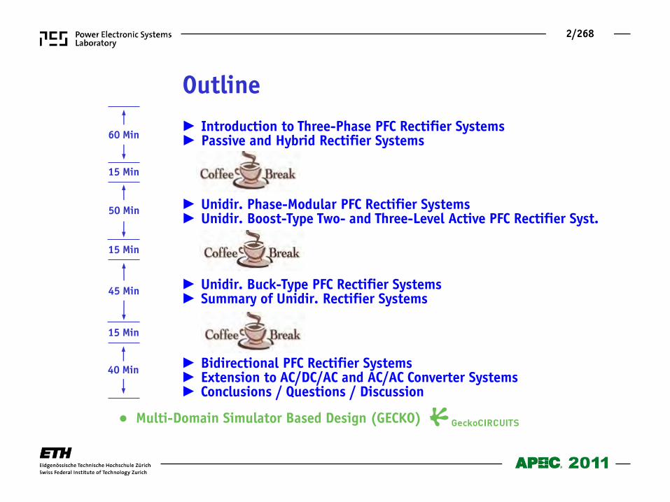
Introduction to Three-Phase PFC Rectifier Systems Passive and Hybrid Rectifier Systems
Outline
60 Min
15 Min
50 Min
15 Min
45 Min
15 Min
40 Min
Multi-Domain Simulator Based Design (GECKO)
Unidir. Phase-Modular PFC Rectifier Systems Unidir. Boost-Type Two- and Three-Level Active PFC Rectifier Syst.
Unidir. Buck-Type PFC Rectifier Systems Summary of Unidir. Rectifier Systems
Bidirectional PFC Rectifier Systems Extension to AC/DC/AC and AC/AC Converter Systems Conclusions / Questions / Discussion
3/268
Part 1
4/268
Three-Phase PFC Rectifier Systems
5/268
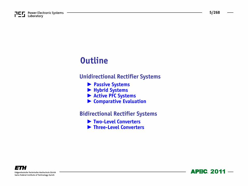
Unidirectional Rectifier Systems Passive Systems Hybrid Systems Active PFC Systems Comparative Evaluation Bidirectional Rectifier Systems Two-Level Converters Three-Level Converters
Outline
6/268
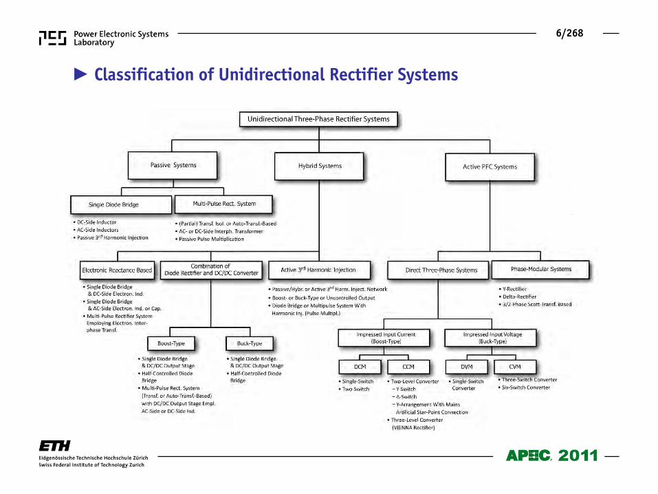
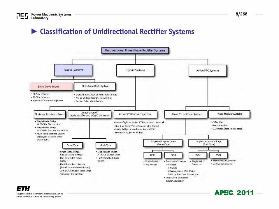
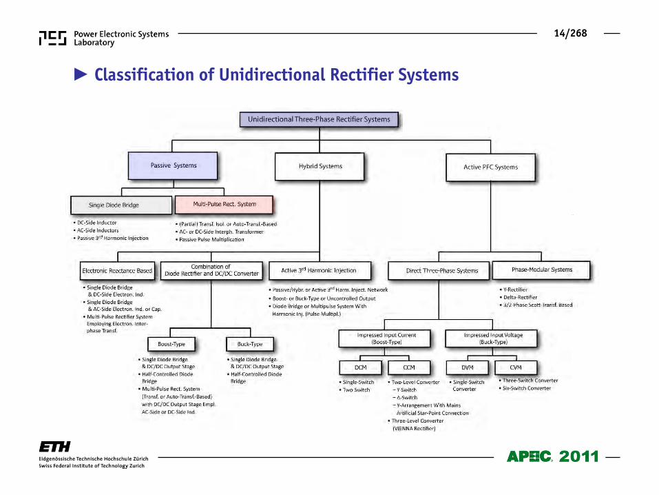
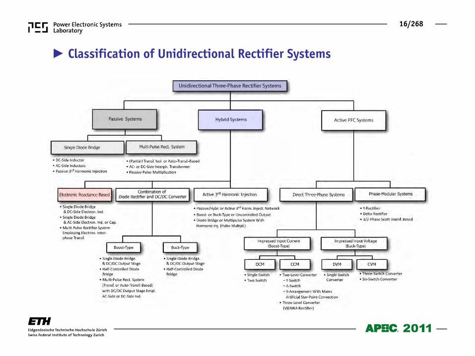
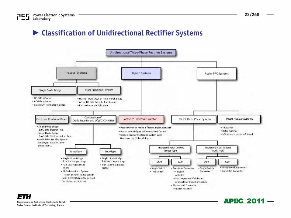
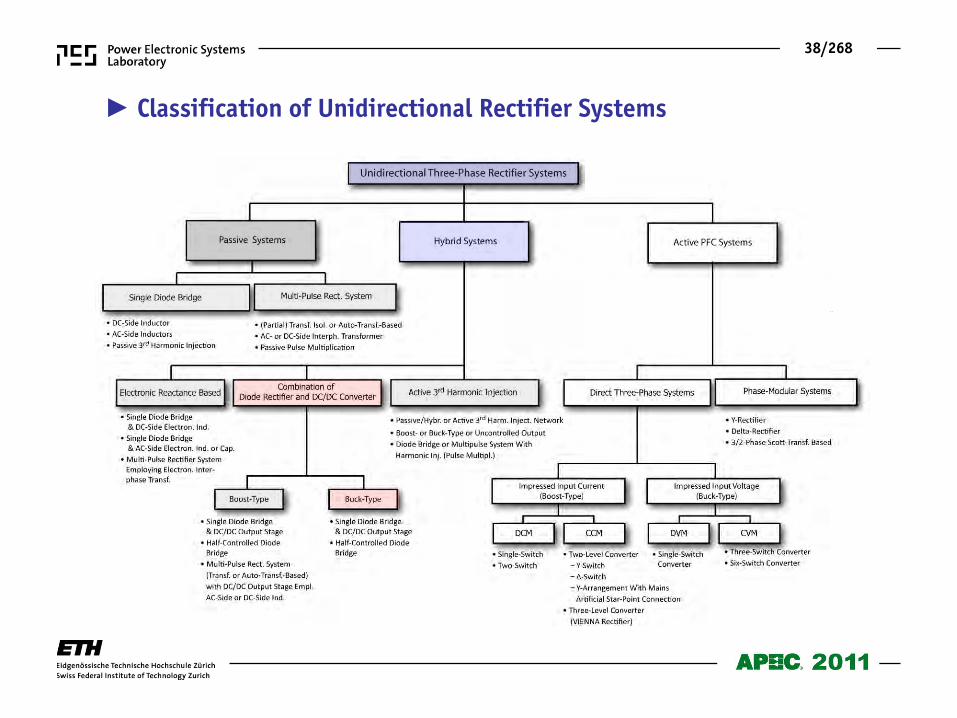
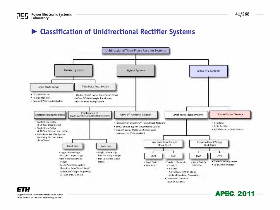
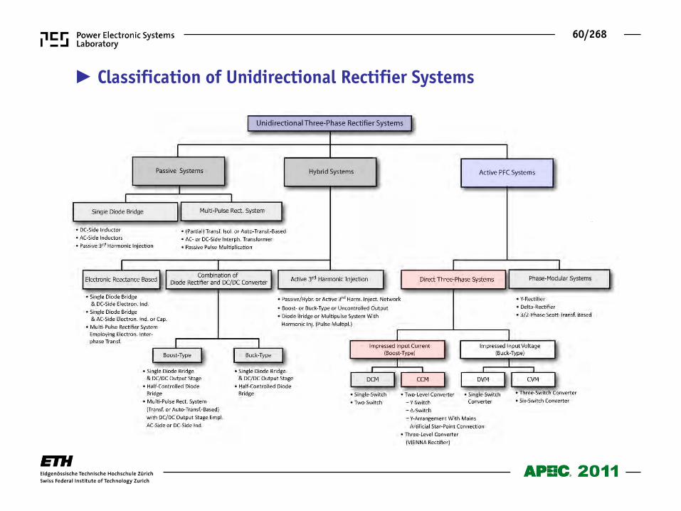
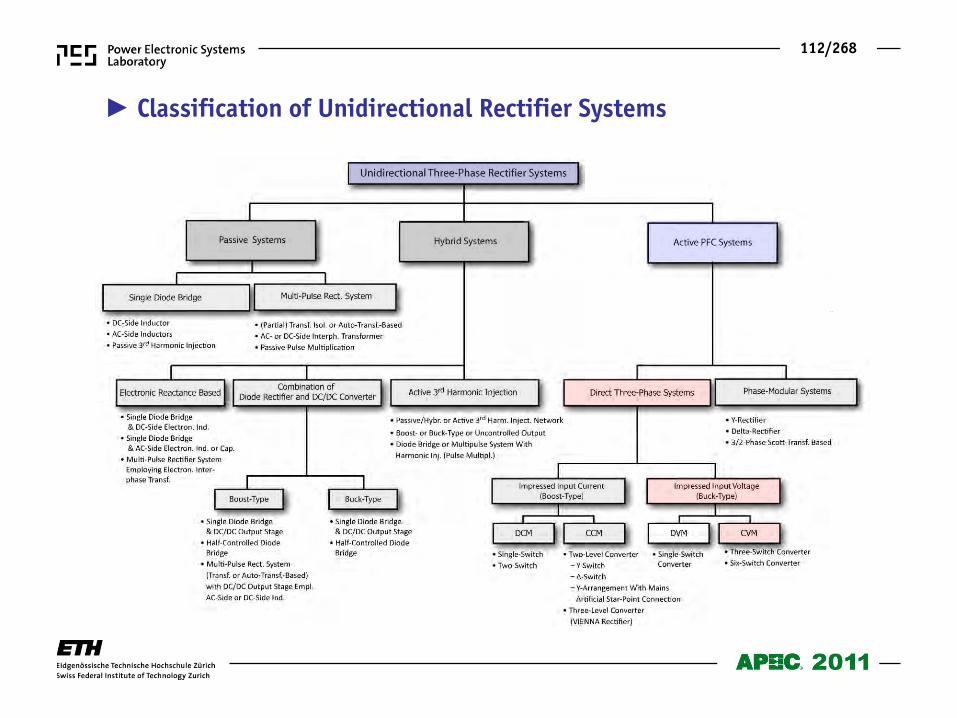
Classification of Unidirectional Rectifier Systems
7/268
Phase-Modular Systems
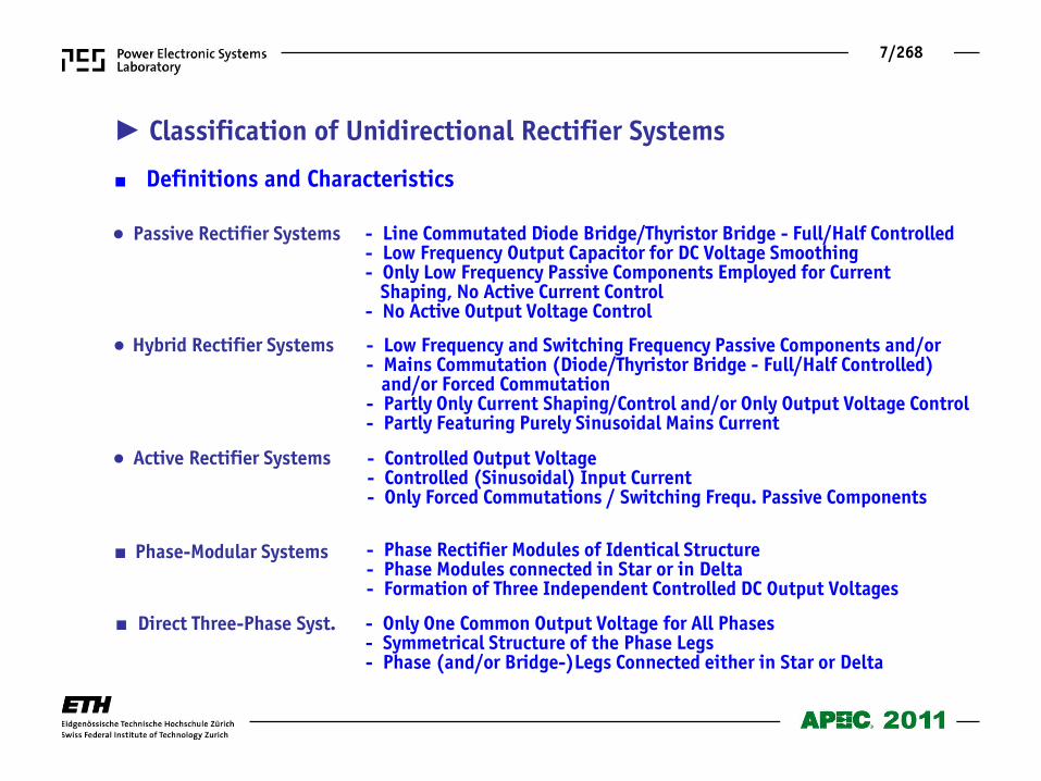
Definitions and Characteristics
Passive Rectifier Systems - Line Commutated Diode Bridge/Thyristor Bridge - Full/Half Controlled - Low Frequency Output Capacitor for DC Voltage Smoothing - Only Low Frequency Passive Components Employed for Current Shaping, No Active Current Control - No Active Output Voltage Control
Hybrid Rectifier Systems - Low Frequency and Switching Frequency Passive Components and/or - Mains Commutation (Diode/Thyristor Bridge - Full/Half Controlled) and/or Forced Commutation - Partly Only Current Shaping/Control and/or Only Output Voltage Control - Partly Featuring Purely Sinusoidal Mains Current
Active Rectifier Systems - Controlled Output Voltage - Controlled (Sinusoidal) Input Current - Only Forced Commutations / Switching Frequ. Passive Components
- Only One Common Output Voltage for All Phases - Symmetrical Structure of the Phase Legs - Phase (and/or Bridge-)Legs Connected either in Star or Delta
Classification of Unidirectional Rectifier Systems
Direct Three-Phase Syst.
- Phase Rectifier Modules of Identical Structure - Phase Modules connected in Star or in Delta - Formation of Three Independent Controlled DC Output Voltages
8/268
Classification of Unidirectional Rectifier Systems
9/268
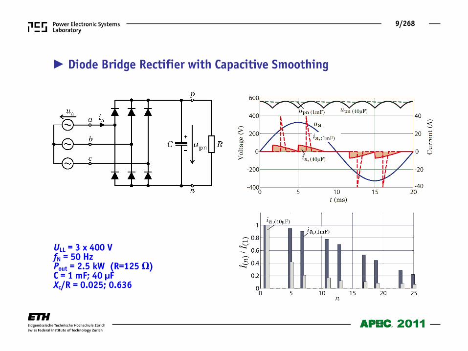
Diode Bridge Rectifier with Capacitive Smoothing
ULL = 3 x 400 V fN = 50 Hz Pout = 2.5 kW (R=125 Ω) C = 1 mF; 40 µF Xc/R = 0.025; 0.636
10/268
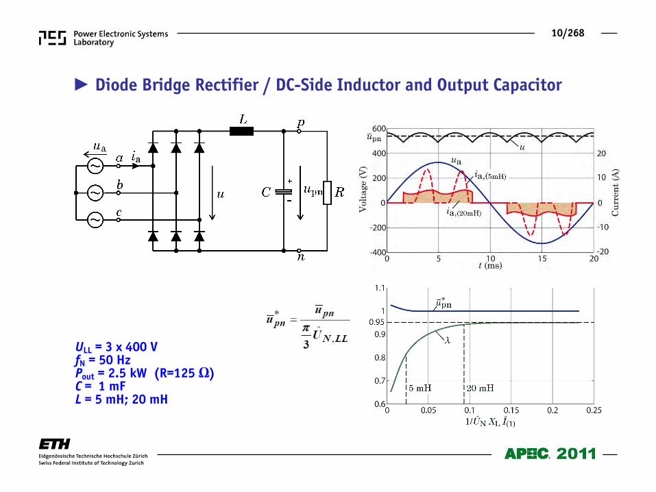
Diode Bridge Rectifier / DC-Side Inductor and Output Capacitor
ULL = 3 x 400 V fN = 50 Hz Pout = 2.5 kW (R=125 Ω) C = 1 mF L = 5 mH; 20 mH
11/268
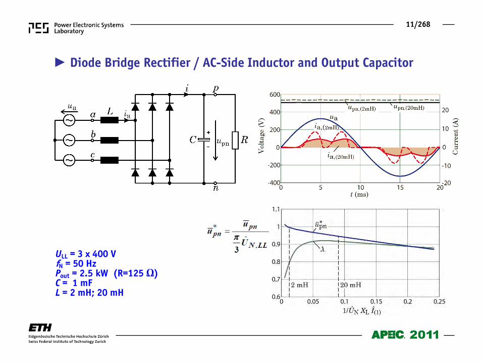
Diode Bridge Rectifier / AC-Side Inductor and Output Capacitor
ULL = 3 x 400 V fN = 50 Hz Pout = 2.5 kW (R=125 Ω) C = 1 mF L = 2 mH; 20 mH
12/268
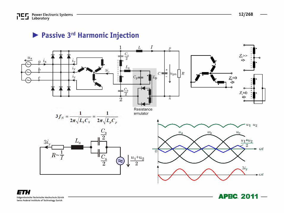
Passive 3rd Harmonic Injection
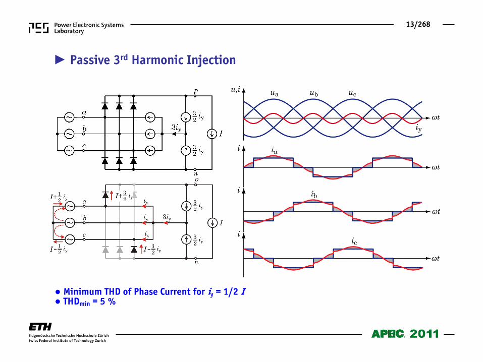
13/268
Minimum THD of Phase Current for iy = 1/2 I THDmin = 5 %
Passive 3rd Harmonic Injection
14/268
Classification of Unidirectional Rectifier Systems
15/268
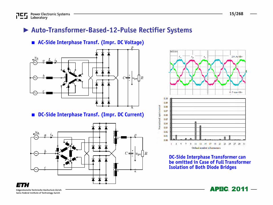
Auto-Transformer-Based-12-Pulse Rectifier Systems
AC-Side Interphase Transf. (Impr. DC Voltage)
DC-Side Interphase Transf. (Impr. DC Current)
20A/Div ia ib ic
0.5ms/Div
DC-Side Interphase Transformer can be omitted in Case of Full Transformer Isolation of Both Diode Bridges
16/268
Classification of Unidirectional Rectifier Systems
17/268
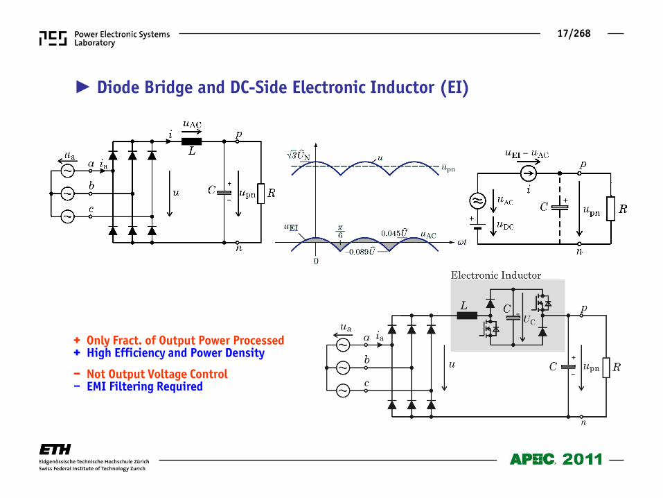
Diode Bridge and DC-Side Electronic Inductor (EI)
+ Only Fract. of Output Power Processed + High Efficiency and Power Density – Not Output Voltage Control – EMI Filtering Required
18/268
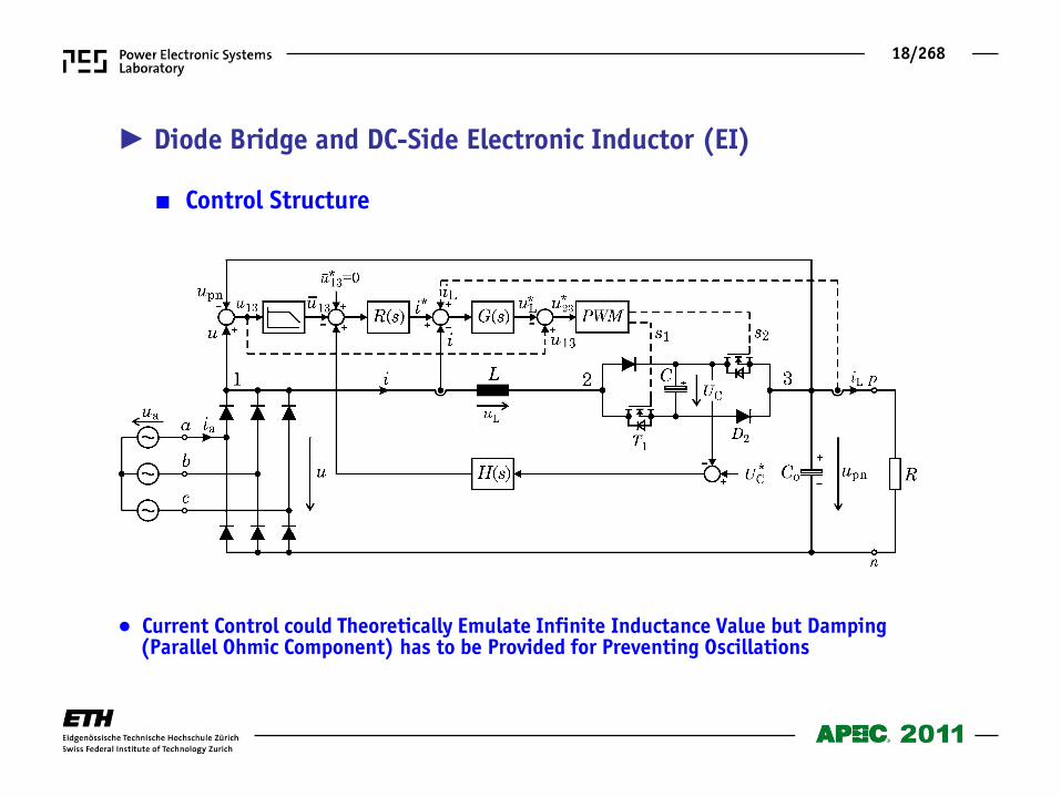
Control Structure
Current Control could Theoretically Emulate Infinite Inductance Value but Damping (Parallel Ohmic Component) has to be Provided for Preventing Oscillations
Diode Bridge and DC-Side Electronic Inductor (EI)
19/268
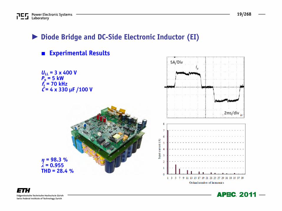
ULL = 3 x 400 V Po = 5 kW fs = 70 kHz C = 4 x 330 µF /100 V
η = 98.3 % λ = 0.955 THD = 28.4 %
ia
2ms/div
Experimental Results
Diode Bridge and DC-Side Electronic Inductor (EI)
5A/Div
20/268
Fundamental Frequency Equivalent Circuit
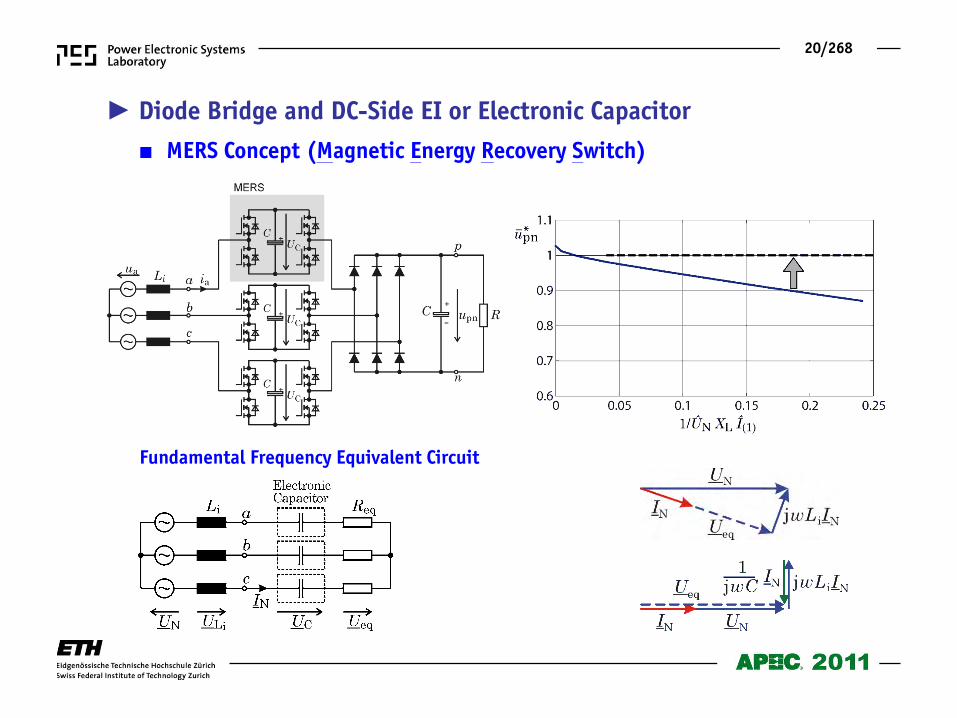
MERS Concept (Magnetic Energy Recovery Switch)
Diode Bridge and DC-Side EI or Electronic Capacitor
21/268
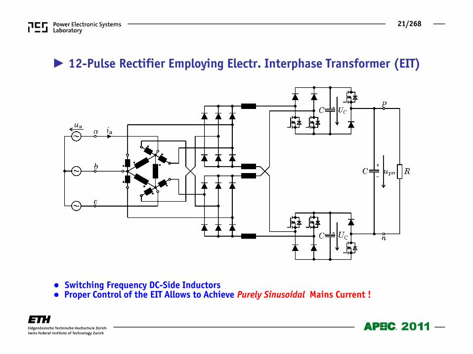
Switching Frequency DC-Side Inductors Proper Control of the EIT Allows to Achieve Purely Sinusoidal Mains Current !
12-Pulse Rectifier Employing Electr. Interphase Transformer (EIT)
22/268
Classification of Unidirectional Rectifier Systems
23/268
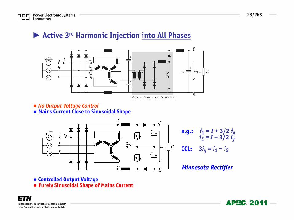
No Output Voltage Control Mains Current Close to Sinusoidal Shape
Controlled Output Voltage Purely Sinusoidal Shape of Mains Current
e.g.: i1 = I + 3/2 iy i2 = I – 3/2 iy CCL: 3iy = i1 – i2
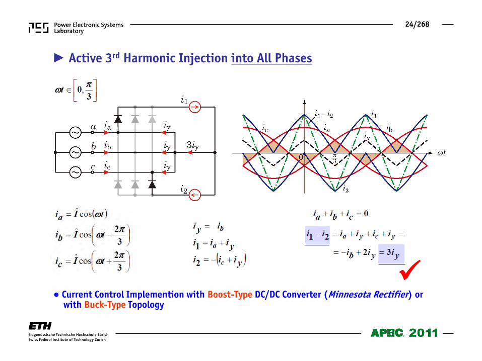
Active 3rd Harmonic Injection into All Phases
Minnesota Rectifier
24/268
Current Control Implemention with Boost-Type DC/DC Converter (Minnesota Rectifier) or with Buck-Type Topology
Active 3rd Harmonic Injection into All Phases
25/268
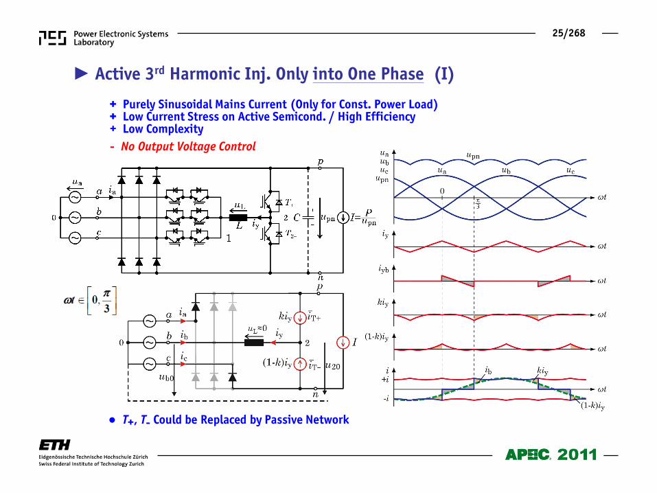
+ Purely Sinusoidal Mains Current (Only for Const. Power Load) + Low Current Stress on Active Semicond. / High Efficiency + Low Complexity
- No Output Voltage Control
Active 3rd Harmonic Inj. Only into One Phase (I)
T+, T- Could be Replaced by Passive Network

26/268
Proof of Sinusoidal Mains Current Shape for
- Current to be Inj. Into Phase b:
- Local Avg. Ind. Voltage / Bridge Leg (T+, T-) Output Voltage:
- Bridge Leg Voltage Formation:
- Bridge Leg Current Formation:
- Constant Power Load Current:
and/or
Sinusoidal Mains Current:
Condition:
27/268
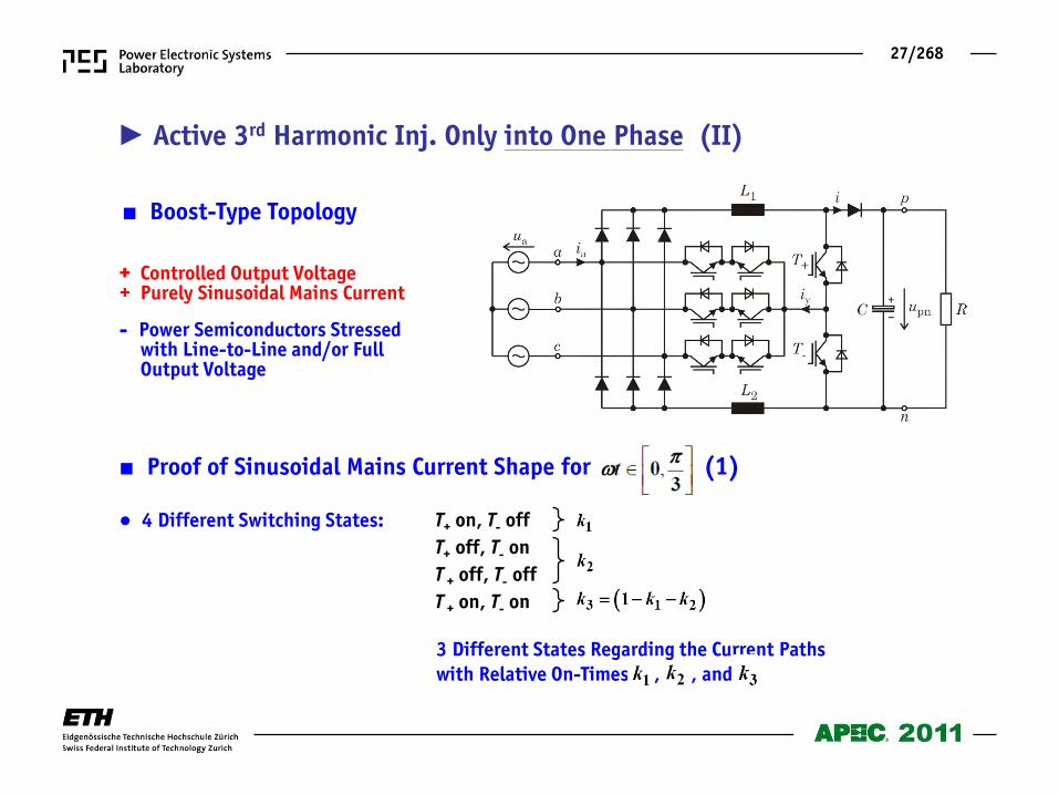
3 Different States Regarding the Current Paths with Relative On-Times , , and
T+ on, T- off T+ off, T- on T + off, T- off T + on, T- on
4 Different Switching States:
Proof of Sinusoidal Mains Current Shape for (1)
Active 3rd Harmonic Inj. Only into One Phase (II)
Boost-Type Topology
+ Controlled Output Voltage + Purely Sinusoidal Mains Current
- Power Semiconductors Stressed with Line-to-Line and/or Full Output Voltage
28/268
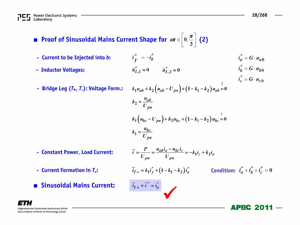
Proof of Sinusoidal Mains Current Shape for (2)
- Current to be Injected into b:
- Inductor Voltages:
- Bridge Leg (T+, T-): Voltage Form.:
- Current Formation in T+:
- Constant Power, Load Current:
Condition:
Sinusoidal Mains Current:
29/268
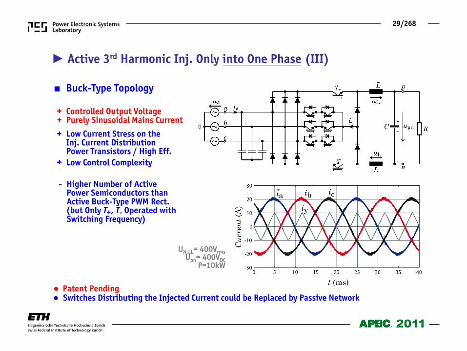
- Higher Number of Active Power Semiconductors than Active Buck-Type PWM Rect. (but Only T+, T- Operated with Switching Frequency)
Active 3rd Harmonic Inj. Only into One Phase (III)
Patent Pending
UN,LL= 400Vrms Upn= 400VDC
P=10kW
+ Controlled Output Voltage + Purely Sinusoidal Mains Current
+ Low Current Stress on the Inj. Current Distribution Power Transistors / High Eff.
+ Low Control Complexity
Switches Distributing the Injected Current could be Replaced by Passive Network
Buck-Type Topology
30/268
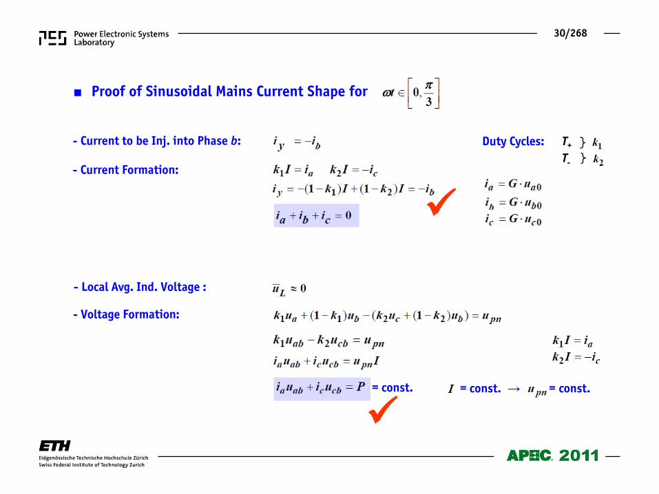
Proof of Sinusoidal Mains Current Shape for
- Current to be Inj. into Phase b:
- Local Avg. Ind. Voltage :
- Current Formation:
- Voltage Formation:
T+ T-
Duty Cycles:
= const. → = const. = const.

31/268
Classification of Unidirectional Rectifier Systems
32/268
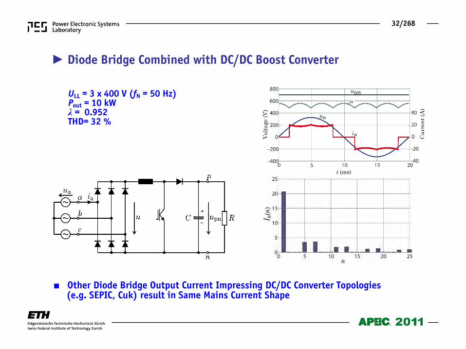
Diode Bridge Combined with DC/DC Boost Converter
Other Diode Bridge Output Current Impressing DC/DC Converter Topologies (e.g. SEPIC, Cuk) result in Same Mains Current Shape
ULL = 3 x 400 V (fN = 50 Hz) Pout = 10 kW λ = 0.952 THD= 32 %
33/268
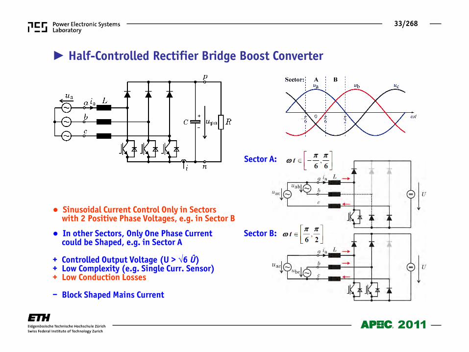
Half-Controlled Rectifier Bridge Boost Converter
Sector A:
Sector B:
Sinusoidal Current Control Only in Sectors with 2 Positive Phase Voltages, e.g. in Sector B In other Sectors, Only One Phase Current could be Shaped, e.g. in Sector A + Controlled Output Voltage (U > √6 Û) + Low Complexity (e.g. Single Curr. Sensor) + Low Conduction Losses – Block Shaped Mains Current
34/268
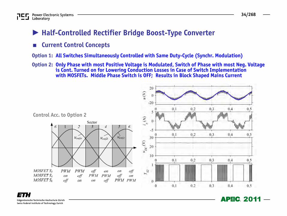
Current Control Concepts
Option 1: All Switches Simultaneously Controlled with Same Duty-Cycle (Synchr. Modulation)
Option 2: Only Phase with most Positive Voltage is Modulated, Switch of Phase with most Neg. Voltage is Cont. Turned on for Lowering Conduction Losses in Case of Switch Implementation with MOSFETs. Middle Phase Switch is OFF; Results in Block Shaped Mains Current
Half-Controlled Rectifier Bridge Boost-Type Converter
Control Acc. to Option 2
35/268
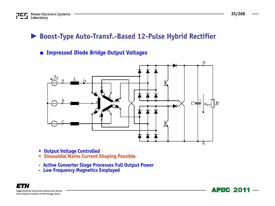
Boost-Type Auto-Transf.-Based 12-Pulse Hybrid Rectifier
+ Output Voltage Controlled + Sinusoidal Mains Current Shaping Possible - Active Converter Stage Processes Full Output Power - Low Frequency Magnetics Employed
Impressed Diode Bridge Output Voltages
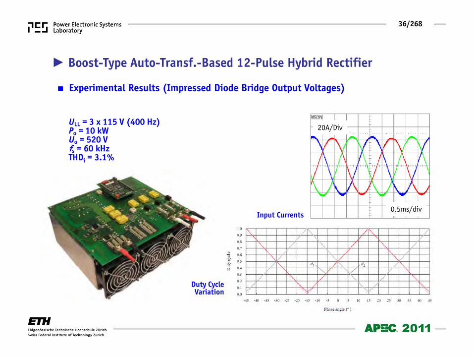
36/268
0.5ms/div
20A/Div
Input Currents
ULL = 3 x 115 V (400 Hz) Po = 10 kW Uo = 520 V fs = 60 kHz THDi = 3.1%
Experimental Results (Impressed Diode Bridge Output Voltages)
Duty Cycle Variation
Boost-Type Auto-Transf.-Based 12-Pulse Hybrid Rectifier
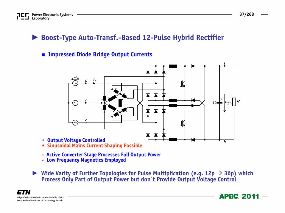
37/268
Wide Varity of Further Topologies for Pulse Multiplication (e.g. 12p 36p) which Process Only Part of Output Power but don´t Provide Output Voltage Control
+ Output Voltage Controlled + Sinusoidal Mains Current Shaping Possible - Active Converter Stage Processes Full Output Power - Low Frequency Magnetics Employed
Boost-Type Auto-Transf.-Based 12-Pulse Hybrid Rectifier
Impressed Diode Bridge Output Currents
38/268
Classification of Unidirectional Rectifier Systems
39/268
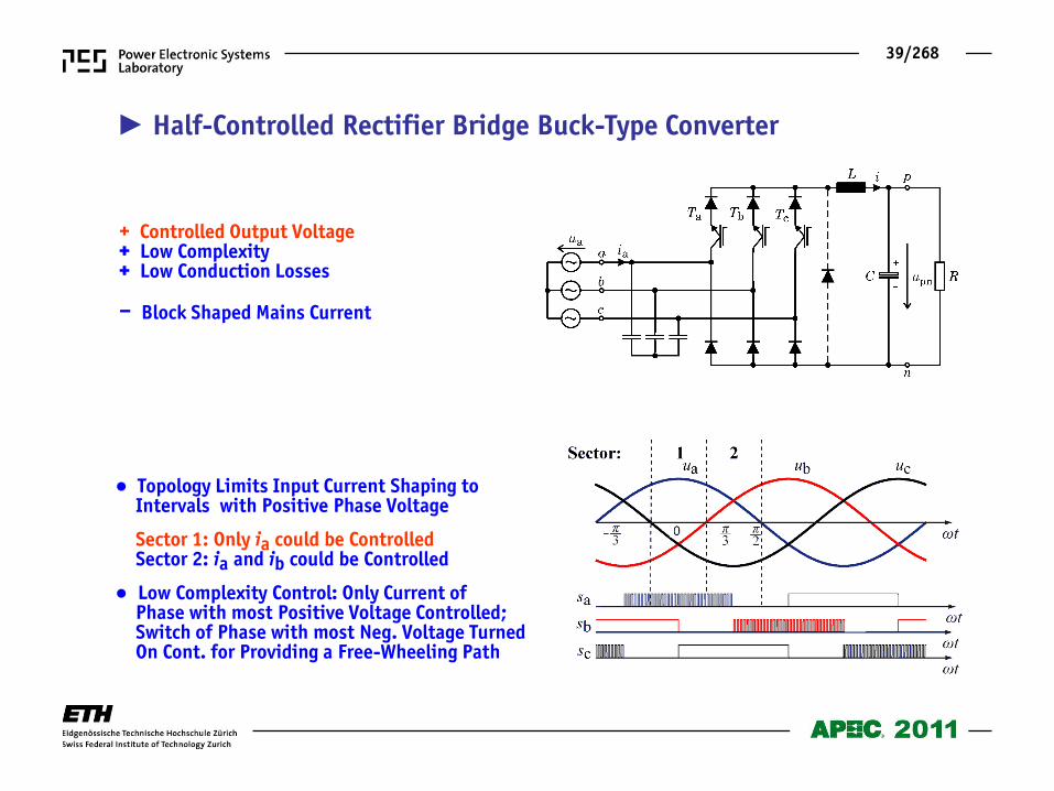
Topology Limits Input Current Shaping to Intervals with Positive Phase Voltage Sector 1: Only ia could be Controlled Sector 2: ia and ib could be Controlled Low Complexity Control: Only Current of Phase with most Positive Voltage Controlled; Switch of Phase with most Neg. Voltage Turned On Cont. for Providing a Free-Wheeling Path
Half-Controlled Rectifier Bridge Buck-Type Converter
+ Controlled Output Voltage + Low Complexity + Low Conduction Losses – Block Shaped Mains Current

40/268
Coffee Break !
41/268
Classification of Unidirectional Rectifier Systems
42/268
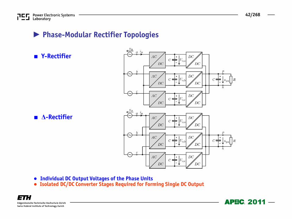
Δ-Rectifier
Y-Rectifier
Individual DC Output Voltages of the Phase Units Isolated DC/DC Converter Stages Required for Forming Single DC Output
Phase-Modular Rectifier Topologies
43/268
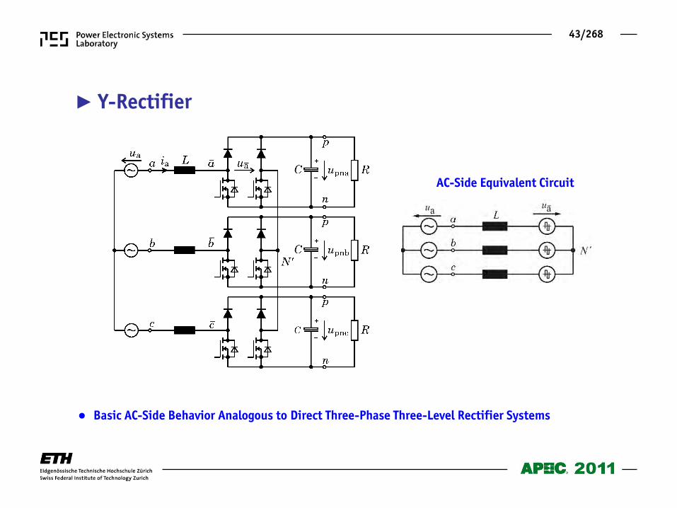
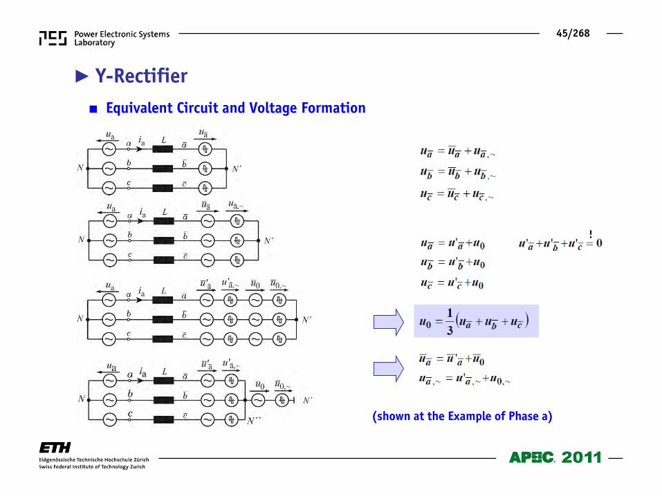
AC-Side Equivalent Circuit
Basic AC-Side Behavior Analogous to Direct Three-Phase Three-Level Rectifier Systems
Y-Rectifier
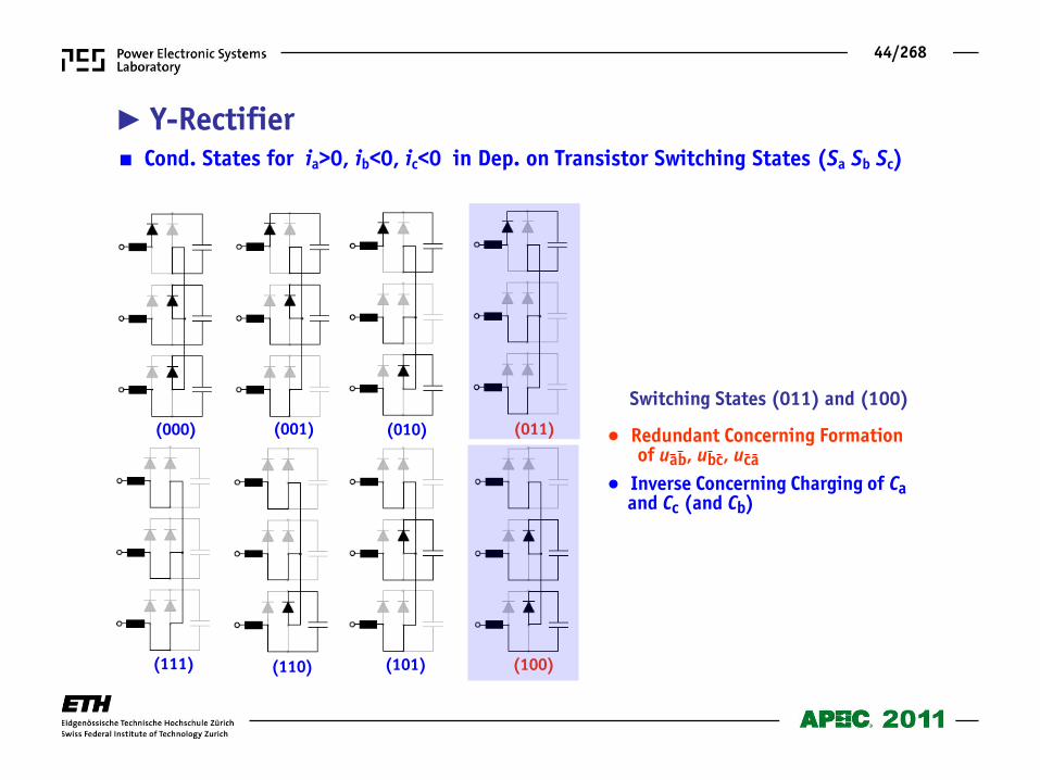
44/268
Cond. States for ia>0, ib<0, ic<0 in Dep. on Transistor Switching States (Sa Sb Sc)
Switching States (011) and (100) (010) (011) (001) (000)
(111) (110) (101) (100)
Y-Rectifier
Redundant Concerning Formation of uab, ubc, uca
Inverse Concerning Charging of Ca and Cc (and Cb)
45/268
(shown at the Example of Phase a)
!
Equivalent Circuit and Voltage Formation
Y-Rectifier
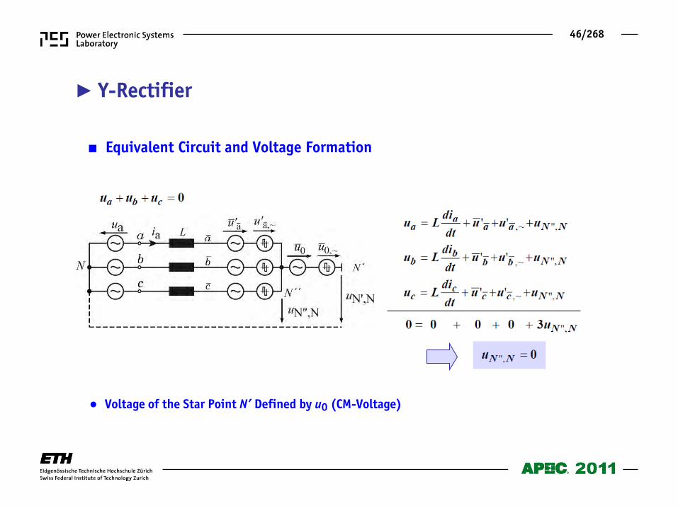
46/268
Voltage of the Star Point N’ Defined by u0 (CM-Voltage)
Equivalent Circuit and Voltage Formation
Y-Rectifier
47/268
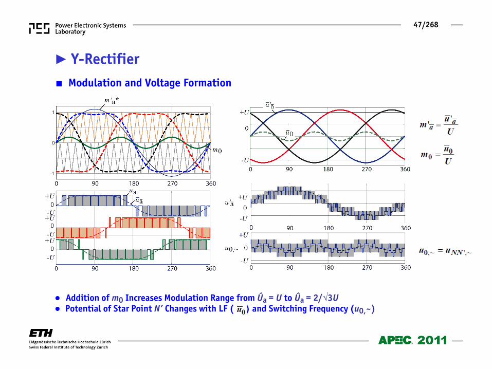
Modulation and Voltage Formation
Addition of m0 Increases Modulation Range from Ûa = U to Ûa = 2/√3U Potential of Star Point N’ Changes with LF ( ) and Switching Frequency (u0,~)
Y-Rectifier
48/268
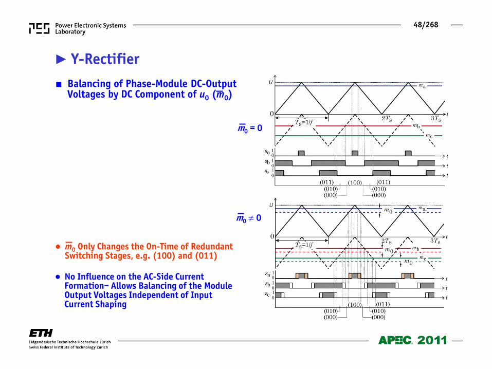
Balancing of Phase-Module DC-Output Voltages by DC Component of u0 (m0)
No Influence on the AC-Side Current Formation– Allows Balancing of the Module Output Voltages Independent of Input Current Shaping
m0 = 0
m0 0
Y-Rectifier
m0 Only Changes the On-Time of Redundant Switching Stages, e.g. (100) and (011)
49/268
VDC,a
VDC,b
VDC,c
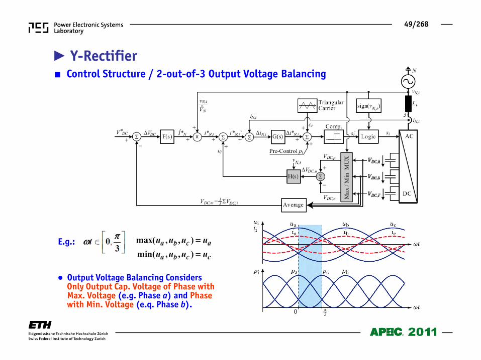
Y-Rectifier Control Structure / 2-out-of-3 Output Voltage Balancing
E.g.:
Output Voltage Balancing Considers Only Output Cap. Voltage of Phase with
Max. Voltage (e.g. Phase a) and Phase with Min. Voltage (e.q. Phase b).
50/268
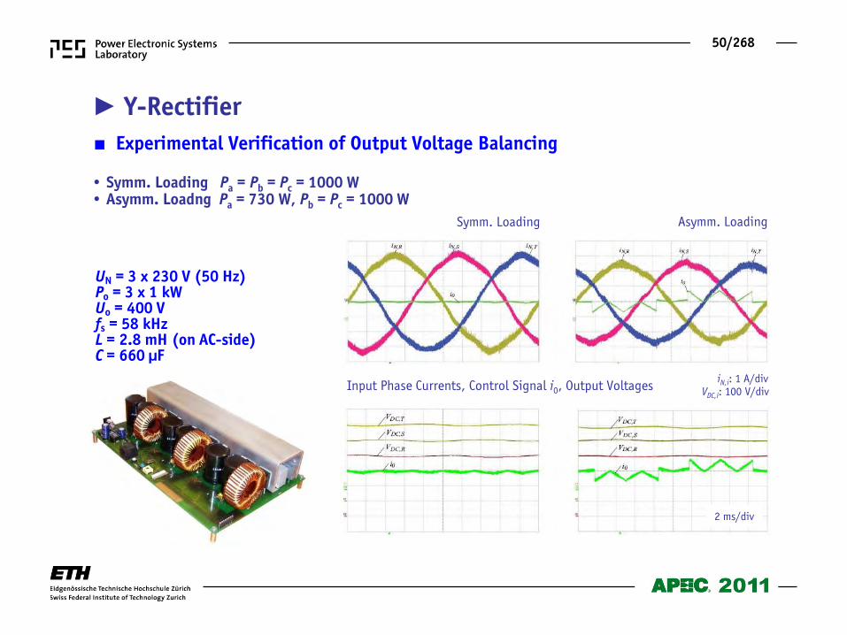
Y-Rectifier Experimental Verification of Output Voltage Balancing
UN = 3 x 230 V (50 Hz) Po = 3 x 1 kW Uo = 400 V fs = 58 kHz L = 2.8 mH (on AC-side) C = 660 µF
Input Phase Currents, Control Signal i0, Output Voltages
• Symm. Loading Pa = Pb = Pc = 1000 W • Asymm. Loadng Pa = 730 W, Pb = Pc = 1000 W
iN,i: 1 A/div VDC,i: 100 V/div
2 ms/div
Symm. Loading Asymm. Loading
51/268
Connection of Each Module to All Phases / Rated Power also Available for Phase Loss !
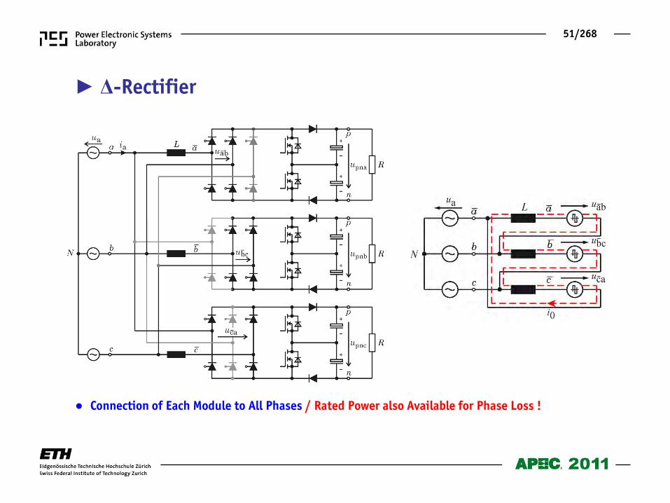
Δ-Rectifier

52/268
Derivation of Equivalent Circuit / Circulating Current Component i0
Δ-Rectifier
Def.:
Mains Phase Current Formed by , , and ua, ub, uc Circulating Current i0 Formed by u0
u0 and/or i0, which does not Appear in ia, ib and ic, can be Maximized by Proper Synchron. of Module PWM Carrier Signals; Accordingly, Switching Frequency Components of , and are Minimized
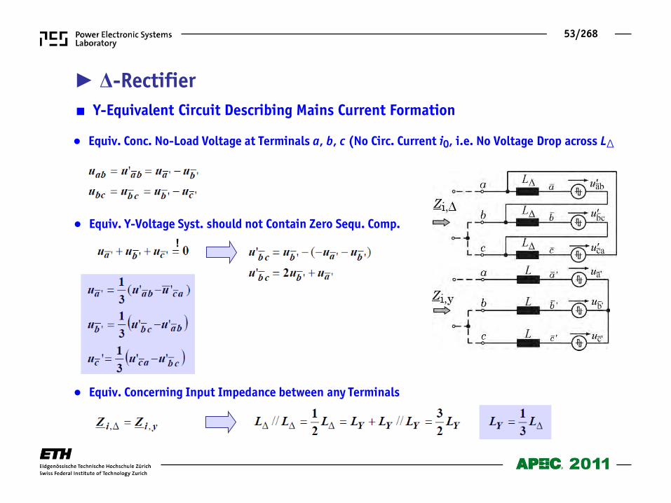
53/268
Equiv. Conc. No-Load Voltage at Terminals a, b, c (No Circ. Current i0, i.e. No Voltage Drop across LΔ
Equiv. Y-Voltage Syst. should not Contain Zero Sequ. Comp.
Equiv. Concerning Input Impedance between any Terminals
Y-Equivalent Circuit Describing Mains Current Formation
!
Δ-Rectifier
54/268
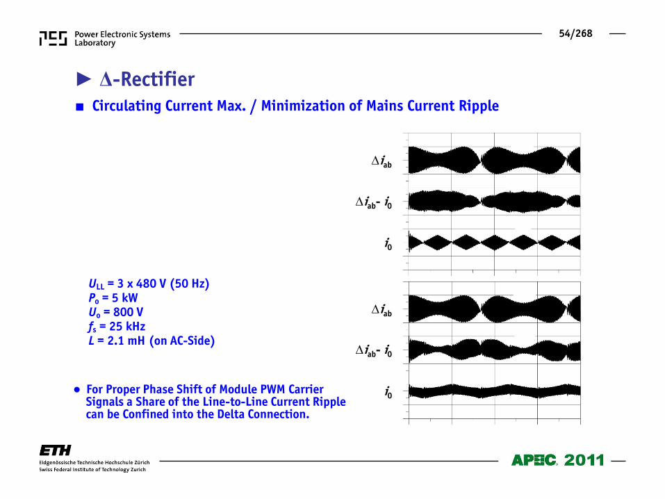
Circulating Current Max. / Minimization of Mains Current Ripple
For Proper Phase Shift of Module PWM Carrier Signals a Share of the Line-to-Line Current Ripple can be Confined into the Delta Connection.
ULL = 3 x 480 V (50 Hz) Po = 5 kW Uo = 800 V fs = 25 kHz L = 2.1 mH (on AC-Side)
iab
iab- i0
i0
iab
iab- i0
i0
Δ-Rectifier
55/268
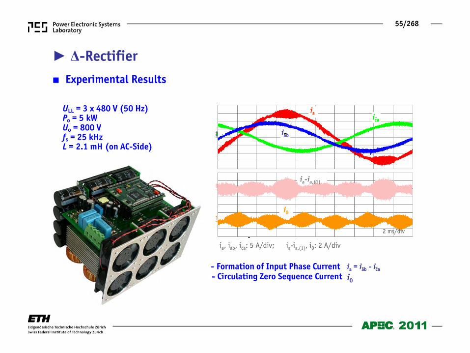
Experimental Results
iab
2 ms/div
ia, iab, ica: 5 A/div; ia-ia,(1), i0: 2 A/div
ia ica
i0
ia-ia,(1)
- Formation of Input Phase Current ia = iab - ica - Circulating Zero Sequence Current i0
Δ-Rectifier
ULL = 3 x 480 V (50 Hz) Po = 5 kW Uo = 800 V fs = 25 kHz L = 2.1 mH (on AC-Side)

56/268
Classification of Unidirectional Rectifier Systems
57/268
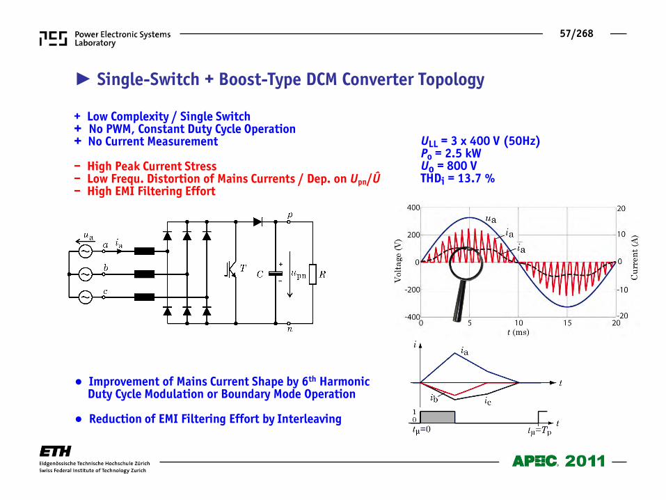
Improvement of Mains Current Shape by 6th Harmonic Duty Cycle Modulation or Boundary Mode Operation Reduction of EMI Filtering Effort by Interleaving
ULL = 3 x 400 V (50Hz) Po = 2.5 kW Uo = 800 V THDi = 13.7 %
Single-Switch + Boost-Type DCM Converter Topology
+ Low Complexity / Single Switch + No PWM, Constant Duty Cycle Operation + No Current Measurement – High Peak Current Stress – Low Frequ. Distortion of Mains Currents / Dep. on Upn/Û – High EMI Filtering Effort
58/268
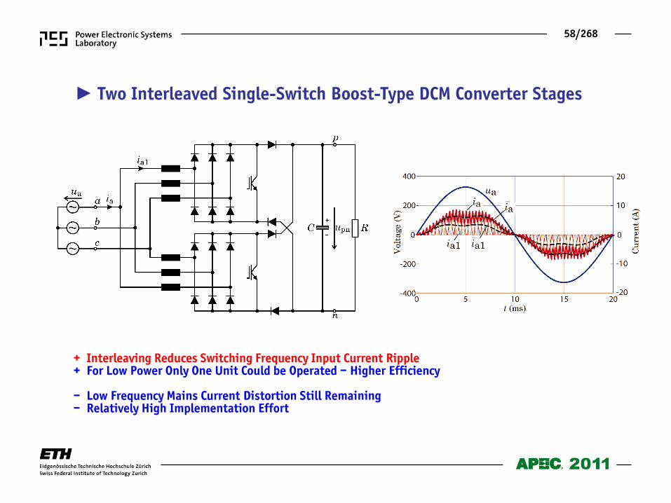
+ Interleaving Reduces Switching Frequency Input Current Ripple + For Low Power Only One Unit Could be Operated – Higher Efficiency – Low Frequency Mains Current Distortion Still Remaining – Relatively High Implementation Effort
Two Interleaved Single-Switch Boost-Type DCM Converter Stages
59/268
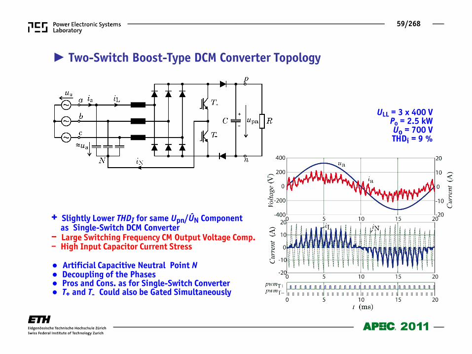
ULL = 3 x 400 V Po = 2.5 kW Uo = 700 V THDi = 9 %
+ Slightly Lower THDI for same Upn/ÛN Component as Single-Switch DCM Converter – Large Switching Frequency CM Output Voltage Comp. – High Input Capacitor Current Stress
Two-Switch Boost-Type DCM Converter Topology
Artificial Capacitive Neutral Point N Decoupling of the Phases Pros and Cons. as for Single-Switch Converter T+ and T- Could also be Gated Simultaneously
60/268
Classification of Unidirectional Rectifier Systems
61/268
Two-Level CCM Boost-Type PFC Rectifier Systems • Y-Switch Rectifier • Δ-Switch Rectifier
62/268
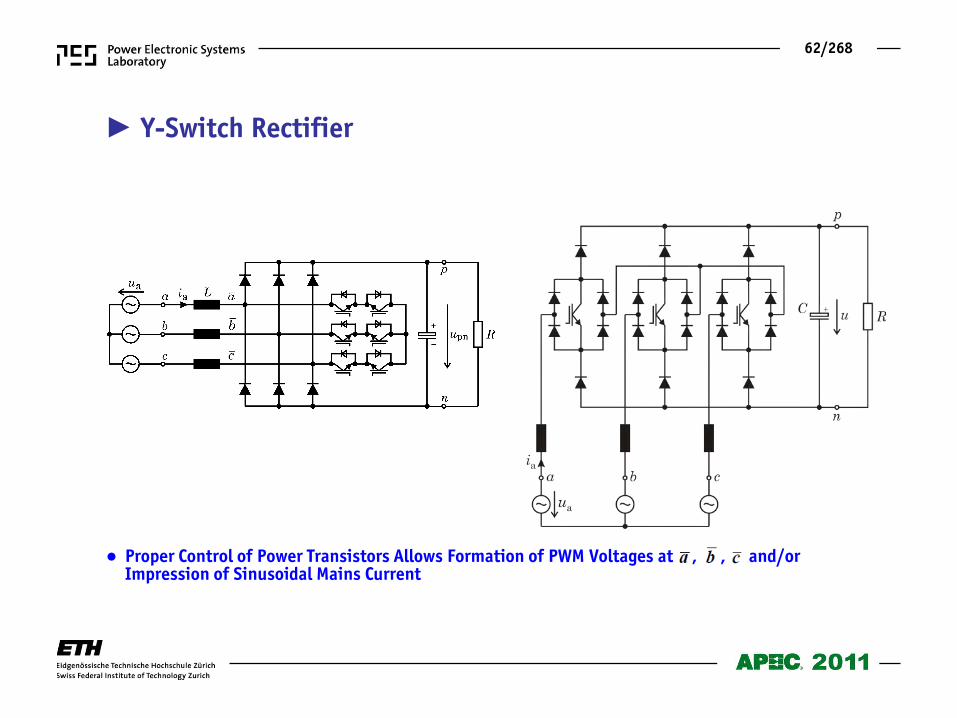
Y-Switch Rectifier
Proper Control of Power Transistors Allows Formation of PWM Voltages at , , and/or Impression of Sinusoidal Mains Current
63/268
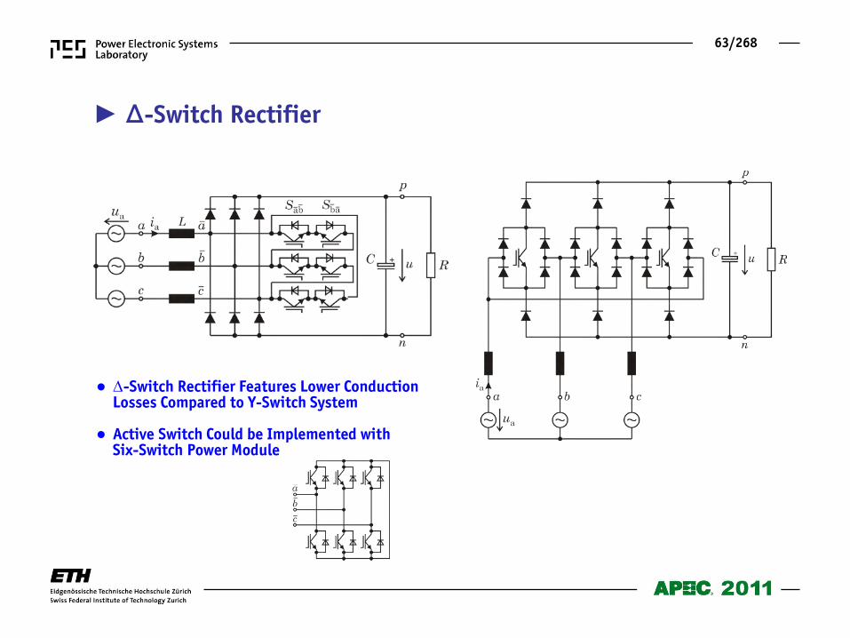
-Switch Rectifier Features Lower Conduction Losses Compared to Y-Switch System Active Switch Could be Implemented with Six-Switch Power Module
Δ-Switch Rectifier

64/268
Reference Voltages, i.e. the Output of the Phase Current Controllers Need to be Transformed into Δ-Quantities
Mains Currents Controlled in Phase with Mains Voltages ua, ub, uc
Voltage Formation at a, b, c is Determined by Switching State of , , and AND Input Current Direction/Magnitude Always Only Switches Corresponding to Highest and Lowest Line-to-Line Voltage are Pulsed Switch of Middle Phase Turned Off Continuously
Equivalent Circuit / Mains Current Control
Δ-Switch Rectifier
65/268
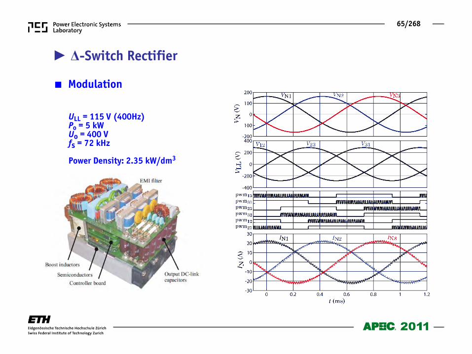
Modulation
Δ-Switch Rectifier
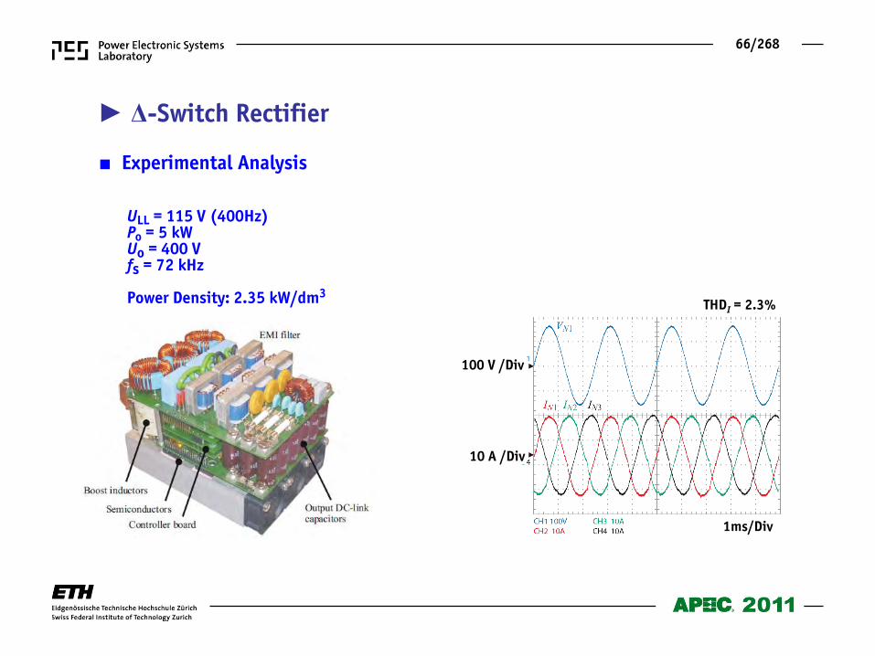
ULL = 115 V (400Hz) Po = 5 kW Uo = 400 V fs = 72 kHz Power Density: 2.35 kW/dm3
66/268
1ms/Div
100 V /Div
10 A /Div
THDI = 2.3%
Experimental Analysis
Δ-Switch Rectifier
ULL = 115 V (400Hz) Po = 5 kW Uo = 400 V fs = 72 kHz Power Density: 2.35 kW/dm3
67/268
Three-Level Boost-Type CCM PFC Rectifier System
• Derivation of Circuit Topologies
68/268
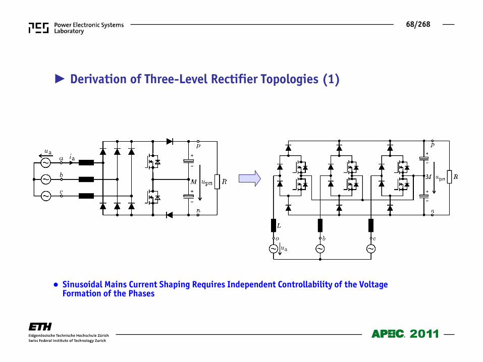
Derivation of Three-Level Rectifier Topologies (1)
Sinusoidal Mains Current Shaping Requires Independent Controllability of the Voltage Formation of the Phases
69/268
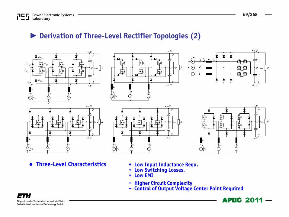
Three-Level Characteristics
Derivation of Three-Level Rectifier Topologies (2)
+ Low Input Inductance Requ. + Low Switching Losses, + Low EMI
– Higher Circuit Complexity – Control of Output Voltage Center Point Required
70/268
Three-Level PFC Rectifier Analysis
• Input Voltage Formation • Modulation / Sinusoidal Input Current Shaping • Output Center Point Formation • Control • Design Considerations • EMI Filtering • Digital Control • Experimental Analysis
71/268
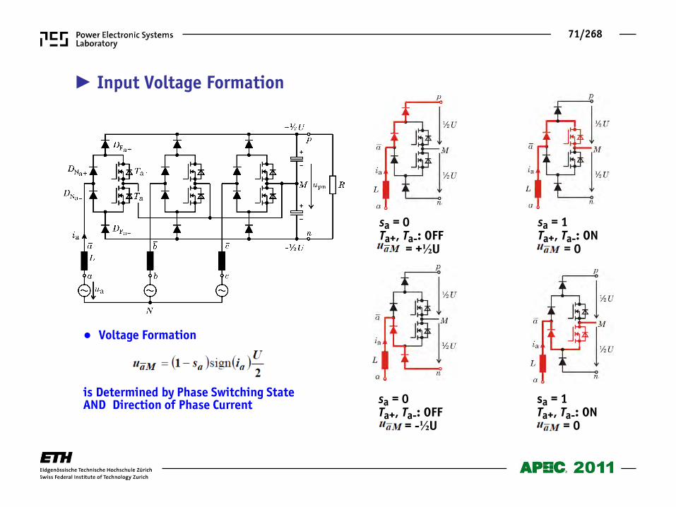
Voltage Formation
is Determined by Phase Switching State AND Direction of Phase Current
Input Voltage Formation
sa = 0 Ta+, Ta-: OFF = +½U
sa = 1 Ta+, Ta-: ON = 0
sa = 0 Ta+, Ta-: OFF = -½U
sa = 1 Ta+, Ta-: ON = 0
72/268
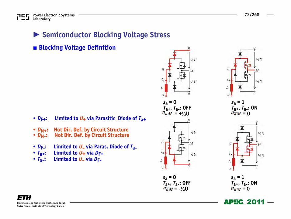
• DF+: Limited to U+ via Parasitic Diode of Ta+ • DN+: Not Dir. Def. by Circuit Structure • DN-: Not Dir. Def. by Circuit Structure • DF-: Limited to U- via Paras. Diode of Ta- • Ta+: Limited to U+ via DF+ • Ta-: Limited to U- via DF-
Semiconductor Blocking Voltage Stress
Blocking Voltage Definition
sa = 0 Ta+, Ta-: OFF = +½U
sa = 1 Ta+, Ta-: ON = 0
sa = 0 Ta+, Ta-: OFF = -½U
sa = 1 Ta+, Ta-: ON = 0
73/268
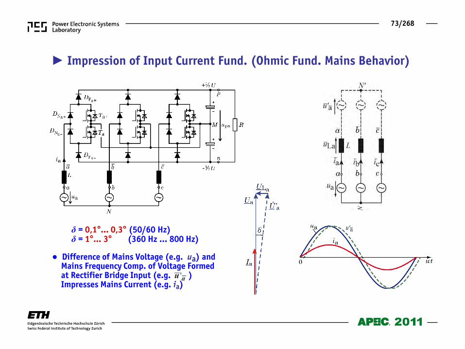
Impression of Input Current Fund. (Ohmic Fund. Mains Behavior)
Difference of Mains Voltage (e.g. ua) and Mains Frequency Comp. of Voltage Formed at Rectifier Bridge Input (e.g. ) Impresses Mains Current (e.g. ia)
δ = 0,1°… 0,3° (50/60 Hz) δ = 1°… 3° (360 Hz … 800 Hz)
74/268
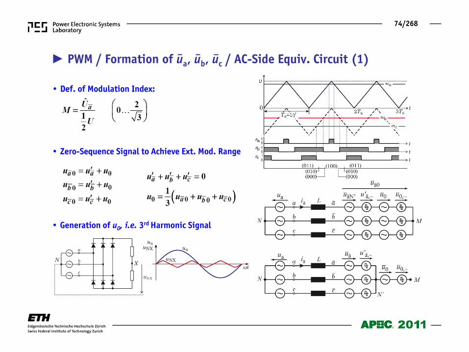
• Def. of Modulation Index:
PWM / Formation of ua, ub, uc / AC-Side Equiv. Circuit (1)
• Zero-Sequence Signal to Achieve Ext. Mod. Range
• Generation of u0, i.e. 3rd Harmonic Signal
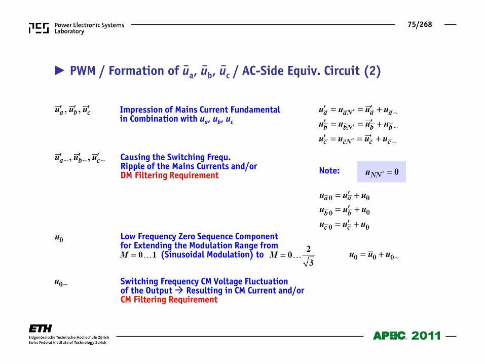
75/268
Low Frequency Zero Sequence Component for Extending the Modulation Range from (Sinusoidal Modulation) to
Impression of Mains Current Fundamental in Combination with ua, ub, uc
Causing the Switching Frequ. Ripple of the Mains Currents and/or DM Filtering Requirement Note:
Switching Frequency CM Voltage Fluctuation of the Output Resulting in CM Current and/or CM Filtering Requirement
PWM / Formation of ua, ub, uc / AC-Side Equiv. Circuit (2)
76/268
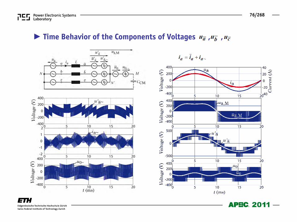
Time Behavior of the Components of Voltages , ,
77/268
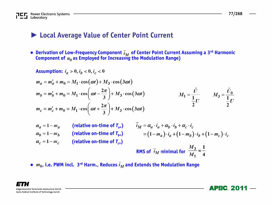
Derivation of Low-Frequency Component of Center Point Current Assuming a 3rd Harmonic Component of (as Employed for Increasing the Modulation Range)
Assumption:
(relative on-time of Ta+)
(relative on-time of Tb+)
(relative on-time of Tc+)
, i.e. PWM incl. 3rd Harm., Reduces and Extends the Modulation Range
Local Average Value of Center Point Current
RMS of minimal for
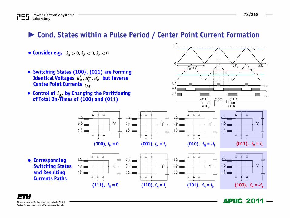
78/268
Switching States (100), (011) are Forming Identical Voltages but Inverse Centre Point Currents
Control of by Changing the Partitioning of Total On-Times of (100) and (011)
Consider e.g.
Corresponding Switching States and Resulting Currents Paths
(000), iM = 0 (001), iM = ia (010), iM = -ib
(111), iM = 0 (110), iM = ic (101), iM = ib
Cond. States within a Pulse Period / Center Point Current Formation
(011), iM = ia
(100), iM = -ia
79/268
System Control • Control Structure • Balancing of the Partial Output Voltages
80/268
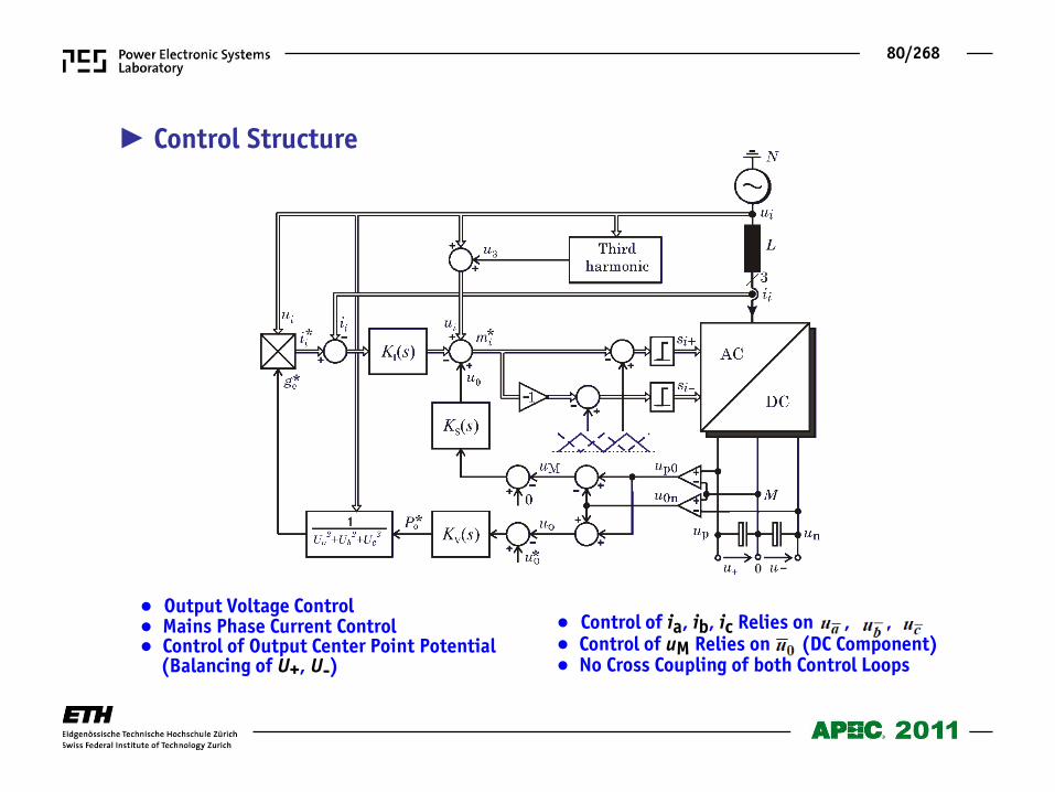
Output Voltage Control Mains Phase Current Control Control of Output Center Point Potential (Balancing of U+, U-)
Control of ia, ib, ic Relies on , , Control of uM Relies on (DC Component) No Cross Coupling of both Control Loops
Control Structure
81/268
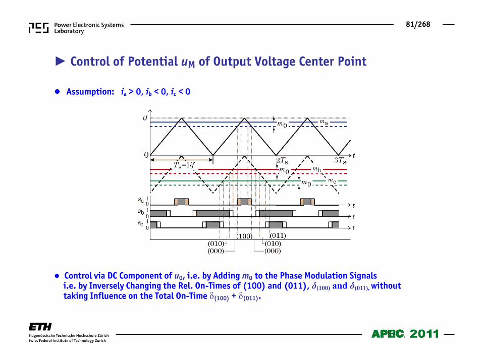
Control via DC Component of u0, i.e. by Adding m0 to the Phase Modulation Signals i.e. by Inversely Changing the Rel. On-Times of (100) and (011), δ(100) and δ(011), without taking Influence on the Total On-Time δ(100) + δ(011).
Assumption: ia > 0, ib < 0, ic < 0
Control of Potential uM of Output Voltage Center Point
82/268
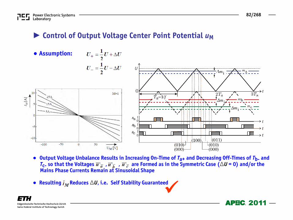
Assumption:
Output Voltage Unbalance Results in Increasing On-Time of Ta+ and Decreasing Off-Times of Tb- and Tc- so that the Voltages , , are Formed as in the Symmetric Case (ΔU = 0) and/or the Mains Phase Currents Remain at Sinusoidal Shape Resulting Reduces ΔU, i.e. Self Stability Guaranteed
Control of Output Voltage Center Point Potential uM
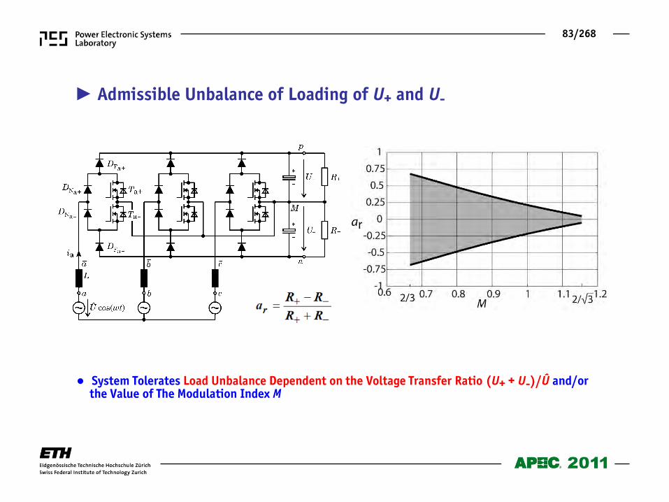
83/268
System Tolerates Load Unbalance Dependent on the Voltage Transfer Ratio (U+ + U-)/Û and/or the Value of The Modulation Index M
Admissible Unbalance of Loading of U+ and U-
84/268
Design Guidelines • Current Stress on the Components • Transistor Selection • Output Pre-Charging at Start-up
85/268
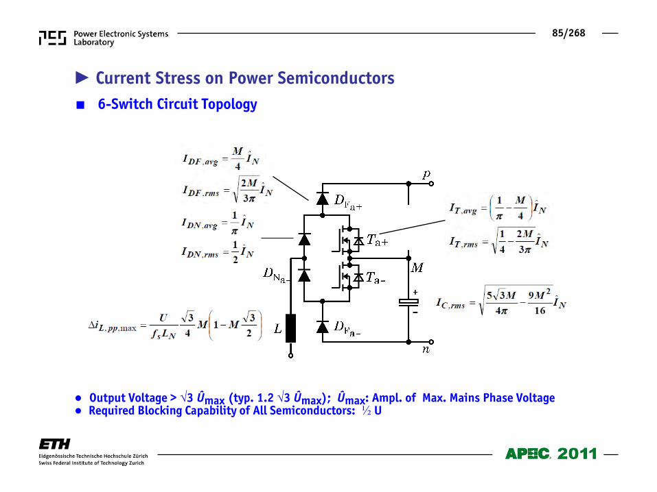
6-Switch Circuit Topology
Current Stress on Power Semiconductors
Output Voltage > √3 Ûmax (typ. 1.2 √3 Ûmax); Ûmax: Ampl. of Max. Mains Phase Voltage Required Blocking Capability of All Semiconductors: ½ U
86/268
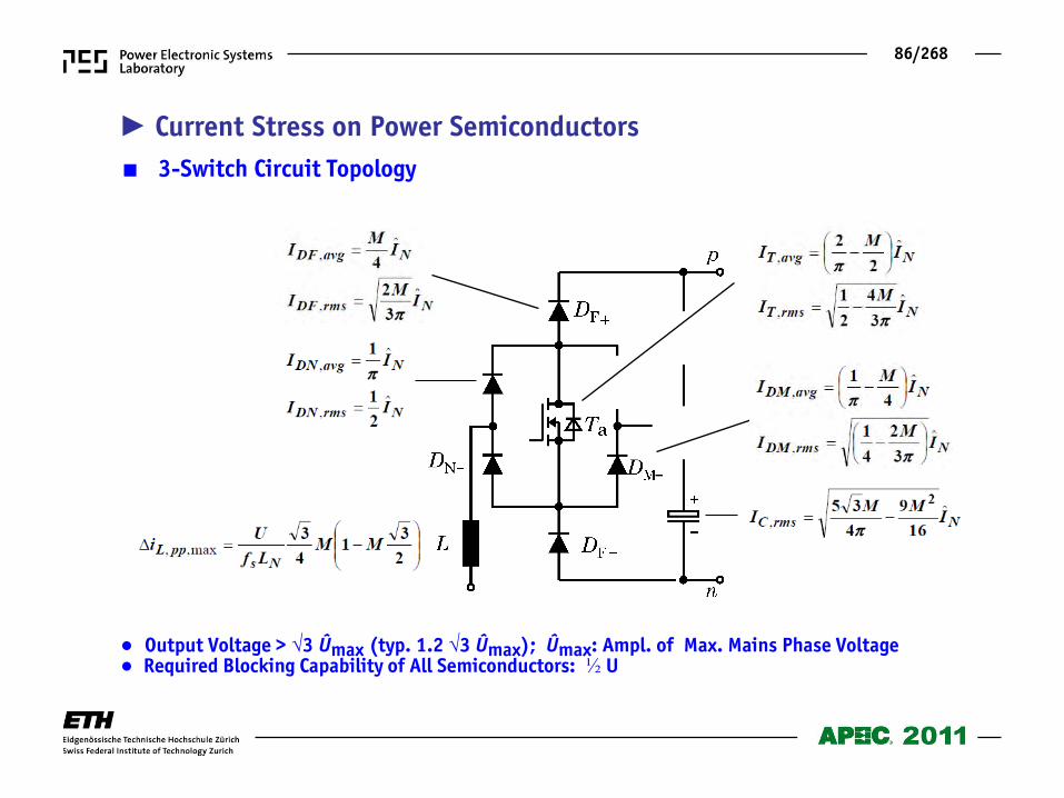
3-Switch Circuit Topology
Current Stress on Power Semiconductors
Output Voltage > √3 Ûmax (typ. 1.2 √3 Ûmax); Ûmax: Ampl. of Max. Mains Phase Voltage Required Blocking Capability of All Semiconductors: ½ U
87/268
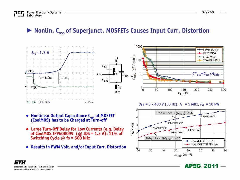
Nonlinear Output Capacitance Coss of MOSFET (CoolMOS) has to be Charged at Turn-off Large Turn-Off Delay for Low Currents (e.g. Delay of CoolMOS IPP60R099 (@ IDS = 1.3 A): 11% of Switching Cycle @ fs = 500 kHz Results in PWM Volt. and/or Input Curr. Distortion
IDS =1.3 A
ULL = 3 x 400 V (50 Hz), fs = 1 MHz, Po = 10 kW
C*oss=Coss/AChip
Nonlin. Coss of Superjunct. MOSFETs Causes Input Curr. Distortion
88/268
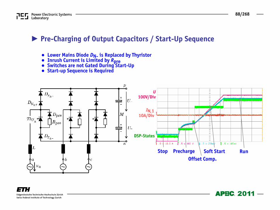
Lower Mains Diode DN- is Replaced by Thyristor Inrush Current is Limited by Rpre Switches are not Gated During Start-Up Start-up Sequence is Required
U 100V/Div
IN,1 10A/Div
DSP-States
Offset Comp. Soft Start Run Stop Precharge
Pre-Charging of Output Capacitors / Start-Up Sequence
89/268
Digital Control Issues • Implementation Using a DSP vs. Using an FPGA • Sampling Strategy • Controller Requirements
90/268
Calculation of Controller Outputs
Current Controller Voltage Controller Balancing of Output Voltages
Startup – Sequence Observe Error Conditions
Over-Voltage at the Output Over-Current Over-Temperature Output Voltage Unbalance
Software Tasks
91/268
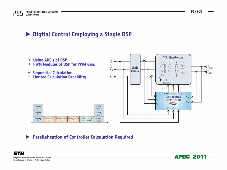
+ Using ADC„s of DSP + PWM Modules of DSP for PWM Gen. – Sequential Calculation – Limited Calculation Capability
Parallelization of Controller Calculation Required
EMC Input Filter
A B C
UN1
iN1
DF-
Thy
N-
DN+
DF+
TM+
TM-
U0 /2
U0 /2
C+
C-
MP
Lboost
+
-
p
n
A1 B1 C1
Digital Control Employing a Single DSP
92/268
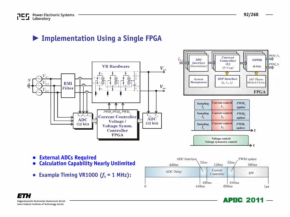
External ADCs Required Calculation Capability Nearly Unlimited Example Timing VR1000 (fs = 1 MHz):
Implementation Using a Single FPGA
93/268
EMC Input Filter
A B C
UN1
iN1
DF-
Thy
N-
DN+
DF+
TM+
TM-
U0 /2
U0 /2
C+
C-
MP
Lboost
+
-
p
n
A1 B1 C1
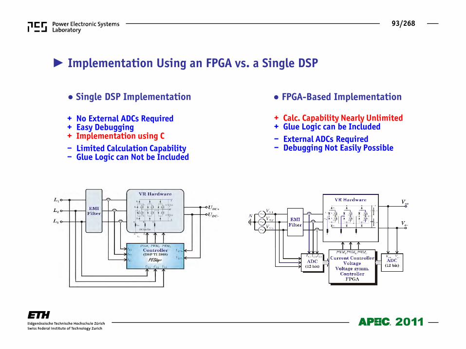
Single DSP Implementation FPGA-Based Implementation
+ No External ADCs Required + Easy Debugging + Implementation using C
– Limited Calculation Capability – Glue Logic can Not be Included
+ Calc. Capability Nearly Unlimited + Glue Logic can be Included
– External ADCs Required – Debugging Not Easily Possible
Implementation Using an FPGA vs. a Single DSP
94/268
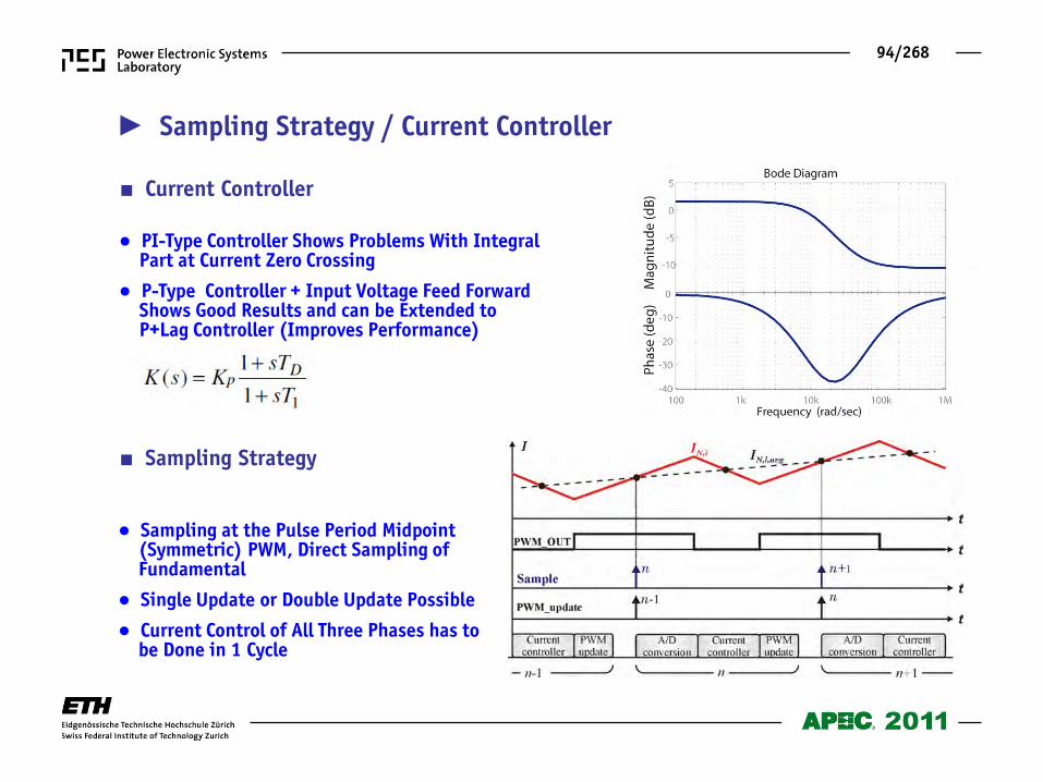
Sampling at the Pulse Period Midpoint (Symmetric) PWM, Direct Sampling of Fundamental
Single Update or Double Update Possible
Current Control of All Three Phases has to be Done in 1 Cycle
PI-Type Controller Shows Problems With Integral Part at Current Zero Crossing
P-Type Controller + Input Voltage Feed Forward Shows Good Results and can be Extended to P+Lag Controller (Improves Performance)
Current Controller
Sampling Strategy / Current Controller
Sampling Strategy
95/268
Output Voltage Controller
Generates Conductance ge for Ref. Value of Current Controller Design for No Steady State Deviation Needs to be Able to Handle Loss of a Mains Phase (Bandwidth << 2fN) Should show Good Dynamical Behavior at Load-Steps
PI-Type – Controller is a Good Choice
Balancing of the Output Voltages
Generates Controller Output u0 (m0) Design for No Steady State Deviation Bandwidth has to be Set Lower than Three Times Mains Frequency fN (Bandwidth << 3fN) Should Show Lowest Dynamic of all Control Loops
PI-Type – Controller is a Good Choice
Output Voltage Controller / Balancing of Partial Output Voltages
96/268
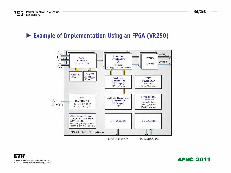
Example of Implementation Using an FPGA (VR250)
97/268
EMI Filtering • DM Filtering • CM Filtering
98/268
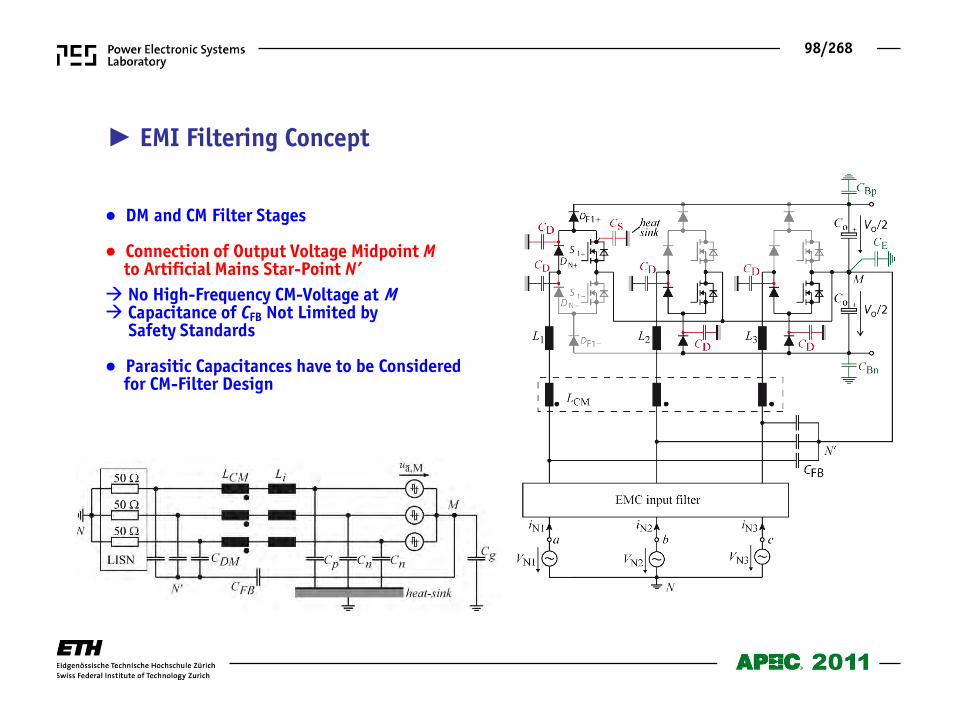
DM and CM Filter Stages Connection of Output Voltage Midpoint M to Artificial Mains Star-Point N’
No High-Frequency CM-Voltage at M Capacitance of CFB Not Limited by Safety Standards Parasitic Capacitances have to be Considered for CM-Filter Design
EMI Filtering Concept
99/268
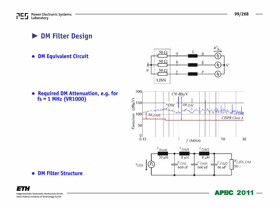
DM Equivalent Circuit
Required DM Attenuation, e.g. for fs = 1 MHz (VR1000)
DM Filter Design
DM Filter Structure
100/268
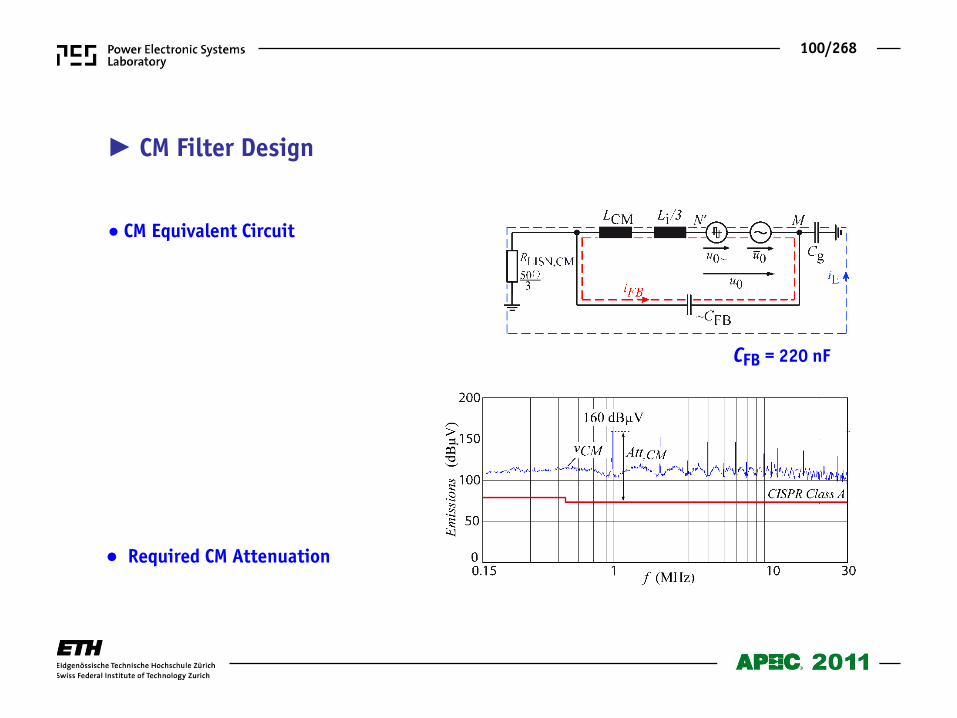
CM Equivalent Circuit
Required CM Attenuation
CFB = 220 nF
CM Filter Design
101/268
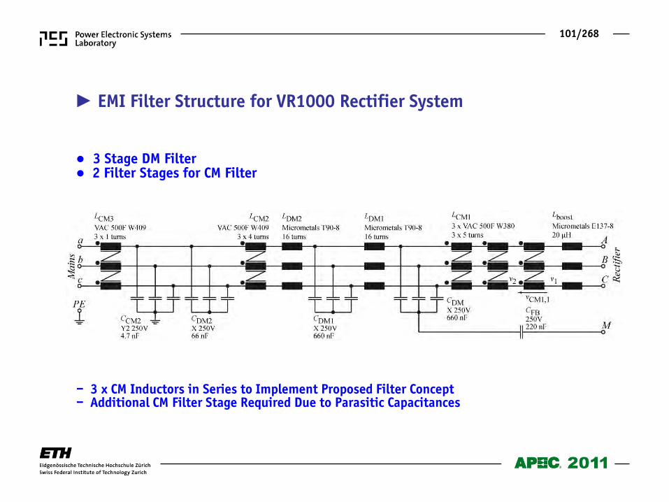
EMI Filter Structure for VR1000 Rectifier System
3 Stage DM Filter 2 Filter Stages for CM Filter
– 3 x CM Inductors in Series to Implement Proposed Filter Concept – Additional CM Filter Stage Required Due to Parasitic Capacitances

102/268
Experimental Analysis • Power Density / Efficiency Pareto Limit • Experimental Analysis – VR250
103/268
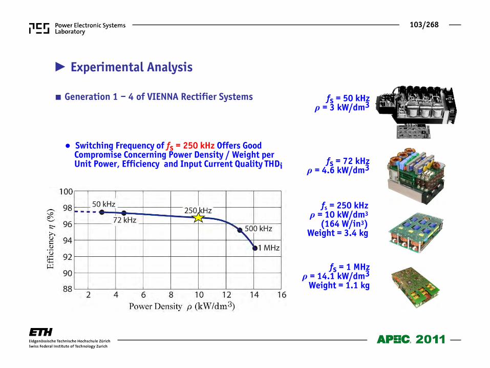
Generation 1 – 4 of VIENNA Rectifier Systems fs = 50 kHz ρ = 3 kW/dm3
fs = 72 kHz ρ = 4.6 kW/dm3
fs = 250 kHz ρ = 10 kW/dm3
(164 W/in3) Weight = 3.4 kg
fs = 1 MHz ρ = 14.1 kW/dm3
Weight = 1.1 kg
Switching Frequency of fs = 250 kHz Offers Good Compromise Concerning Power Density / Weight per Unit Power, Efficiency and Input Current Quality THDi
Experimental Analysis
104/268
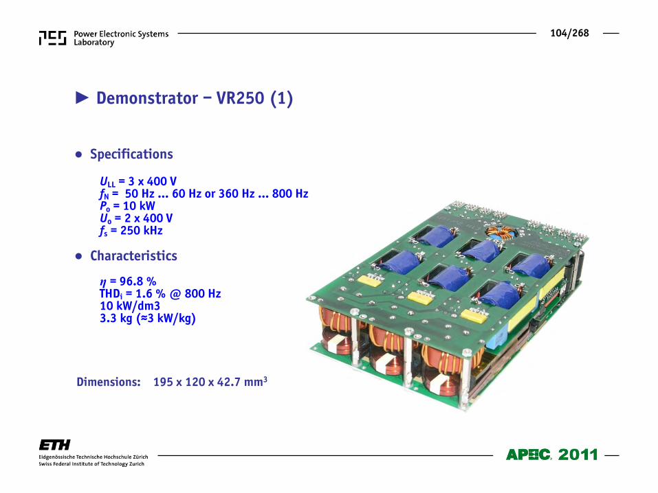
Specifications ULL = 3 x 400 V fN = 50 Hz … 60 Hz or 360 Hz … 800 Hz Po = 10 kW Uo = 2 x 400 V fs = 250 kHz Characteristics η = 96.8 % THDi = 1.6 % @ 800 Hz 10 kW/dm3 3.3 kg (≈3 kW/kg)
Dimensions: 195 x 120 x 42.7 mm3
Demonstrator – VR250 (1)
105/268
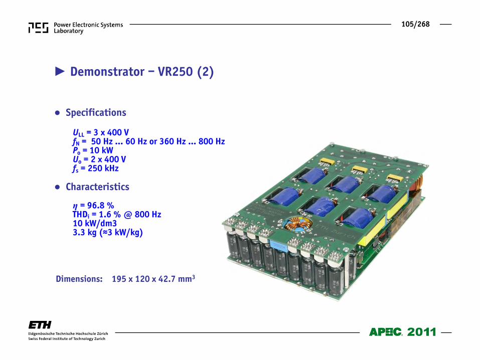
Specifications ULL = 3 x 400 V fN = 50 Hz … 60 Hz or 360 Hz … 800 Hz Po = 10 kW Uo = 2 x 400 V fs = 250 kHz Characteristics η = 96.8 % THDi = 1.6 % @ 800 Hz 10 kW/dm3 3.3 kg (≈3 kW/kg)
Dimensions: 195 x 120 x 42.7 mm3
Demonstrator – VR250 (2)
106/268
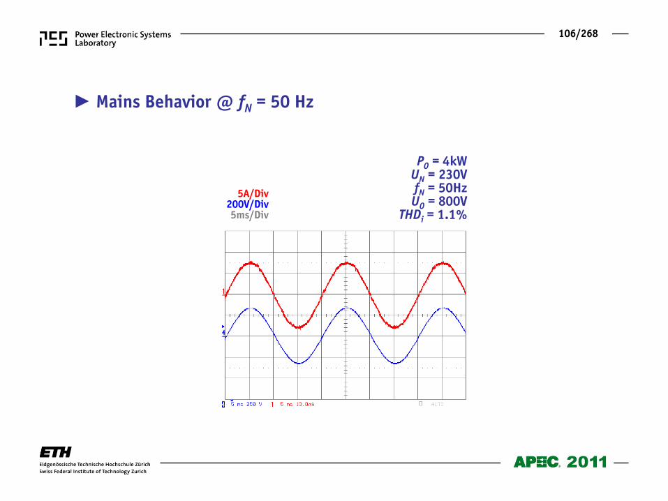
5A/Div
200V/Div 5ms/Div
PO = 4kW UN = 230V fN = 50Hz UO = 800V
THDi = 1.1%
Mains Behavior @ fN = 50 Hz
107/268
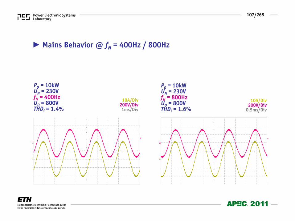
10A/Div
200V/Div 0.5ms/Div
PO = 10kW UN = 230V fN = 400Hz UO = 800V THDi = 1.4%
10A/Div
200V/Div 1ms/Div
PO = 10kW UN = 230V fN = 800Hz UO = 800V THDi = 1.6%
Mains Behavior @ fN = 400Hz / 800Hz
108/268
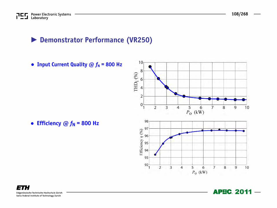
Efficiency @ fN = 800 Hz
Input Current Quality @ fN = 800 Hz
Demonstrator Performance (VR250)
109/268
20 ms/Div
Uo 250 V/div
I N 5 A/div
20 ms/Div
Uo 250 V/div
I N 5 A/div
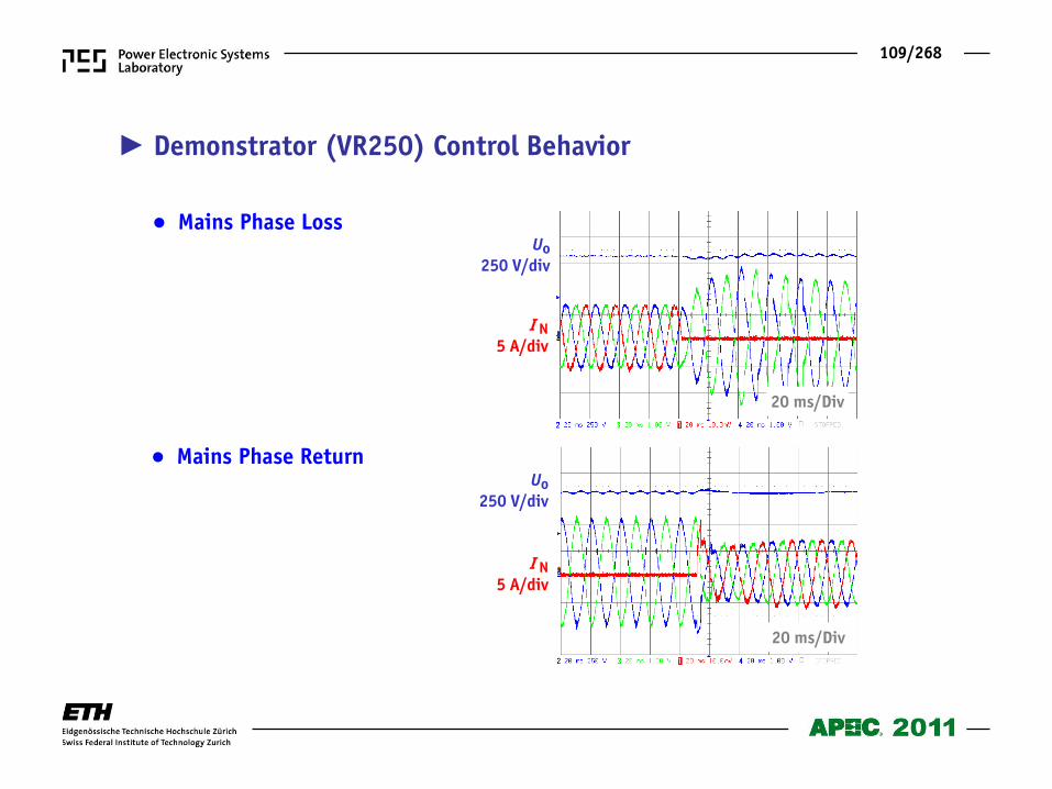
Demonstrator (VR250) Control Behavior
Mains Phase Loss
Mains Phase Return
110/268
dBµV
dBµV
SGL
TDS
150 kHz 30 MHz
RBW 9 kHz
PREAMP OFFAtt 10 dB AUTO
2 QP
VIEW
MT 100 ms
6DB
PRN
1 MHz 10 MHz
0
10
20
30
40
50
60
70
80
90
100
CLASSA_Q
Date: 23.DEC.2009 14:18:11
dBµV
dBµV
SGL
TDS
150 kHz 30 MHz
RBW 9 kHz
PREAMP OFFAtt 10 dB AUTO
3 QP
VIEW
MT 100 ms
6DB
PRN
1 MHz 10 MHz
0
10
20
30
40
50
60
70
80
90
100
CLASSA_Q
Date: 23.DEC.2009 14:17:40
dBµV
dBµV
SGL
TDS
150 kHz 30 MHz
RBW 9 kHz
PREAMP OFFAtt 10 dB AUTO
1 QP
VIEW
MT 100 ms
6DB
PRN
1 MHz 10 MHz
0
10
20
30
40
50
60
70
80
90
100
CLASSA_Q
Date: 23.DEC.2009 14:18:39
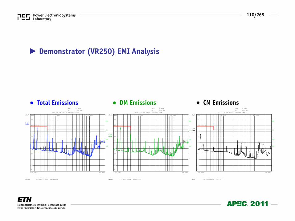
Demonstrator (VR250) EMI Analysis
Total Emissions DM Emissions CM Emissions

111/268
Coffee Break !
112/268
Classification of Unidirectional Rectifier Systems
113/268
Buck-Type CVM PFC Rectifier System
• Derivation of Circuit Topologies
114/268
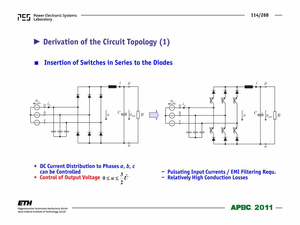
Derivation of the Circuit Topology (1)
Insertion of Switches in Series to the Diodes
+ DC Current Distribution to Phases a, b, c can be Controlled + Control of Output Voltage
– Pulsating Input Currents / EMI Filtering Requ. – Relatively High Conduction Losses
115/268
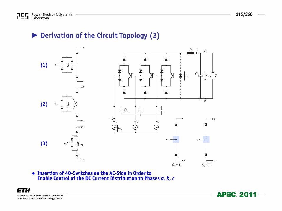
Insertion of 4Q-Switches on the AC-Side in Order to Enable Control of the DC Current Distribution to Phases a, b, c
(1)
(2)
(3)
Derivation of the Circuit Topology (2)
116/268
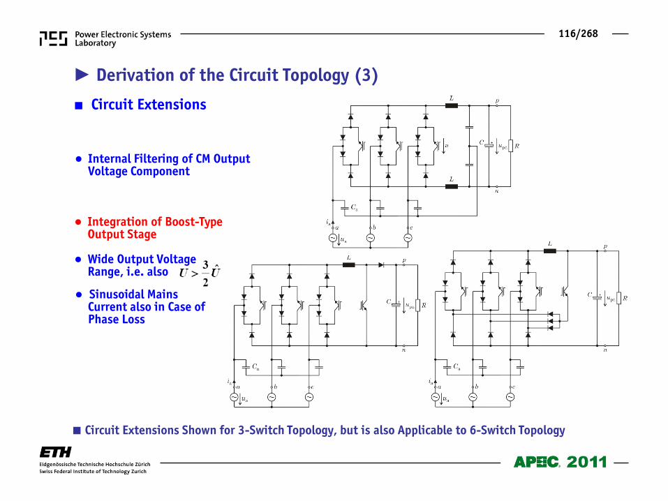
Circuit Extensions
Internal Filtering of CM Output Voltage Component
Integration of Boost-Type Output Stage Wide Output Voltage Range, i.e. also
Derivation of the Circuit Topology (3)
Circuit Extensions Shown for 3-Switch Topology, but is also Applicable to 6-Switch Topology
Sinusoidal Mains Current also in Case of Phase Loss
117/268
Buck-Type PFC Rectifier Analysis
• Modulation • Input Current Formation • Output Voltage Formation • Experimental Analysis
118/268
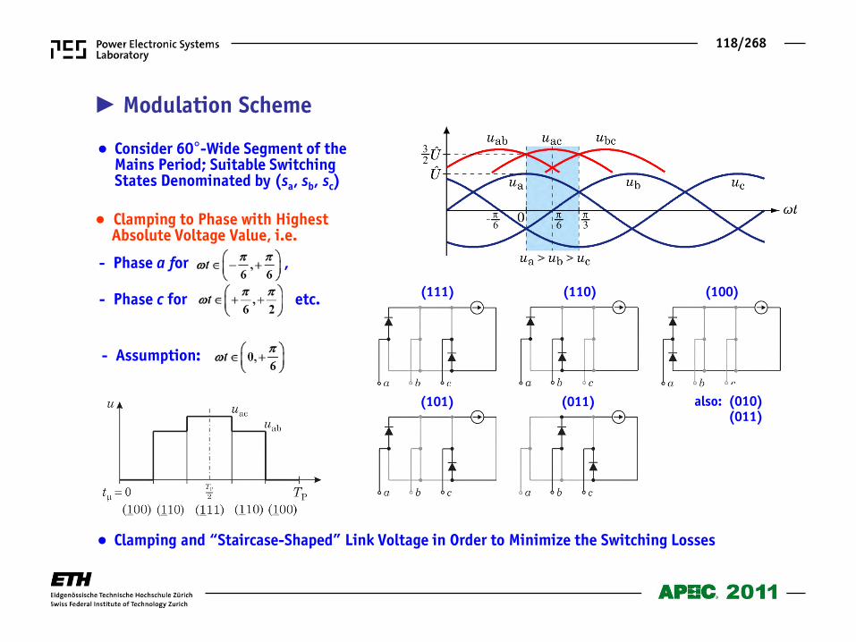
Consider 60°-Wide Segment of the Mains Period; Suitable Switching States Denominated by (sa, sb, sc)
Clamping and “Staircase-Shaped” Link Voltage in Order to Minimize the Switching Losses
(111) (110) (100)
(101) (011) also: (010) (011)
Modulation Scheme
- Assumption:
- Phase c for etc.
- Phase a for ,
Clamping to Phase with Highest Absolute Voltage Value, i.e.
119/268
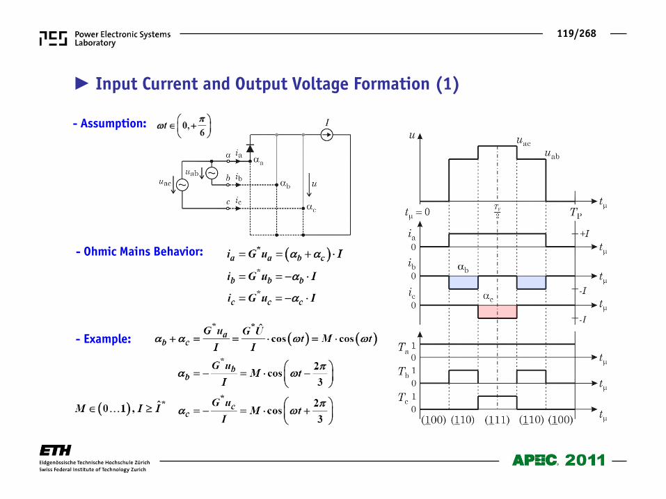
- Ohmic Mains Behavior:
- Example:
Input Current and Output Voltage Formation (1)
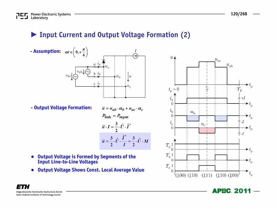
- Assumption:
120/268
Input Current and Output Voltage Formation (2)
Output Voltage is Formed by Segments of the Input Line-to-Line Voltages
Output Voltage Shows Const. Local Average Value
- Output Voltage Formation:
- Assumption:
121/268
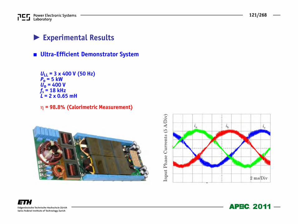
Ultra-Efficient Demonstrator System
Experimental Results
ULL = 3 x 400 V (50 Hz) Po = 5 kW Uo = 400 V fs = 18 kHz L = 2 x 0.65 mH = 98.8% (Calorimetric Measurement)

122/268
Ultra-Efficient Demonstrator System
Experimental Results
ULL = 3 x 400 V (50 Hz) Po = 5 kW Uo = 400 V fs = 18 kHz L = 2 x 0.65 mH = 98.8% (Calorimetric Measurement)
123/268
Summary of Unidirectional PFC Rectifier Systems
• Block Shaped Input Current Systems • Sinusoidal Input Current Systems
124/268
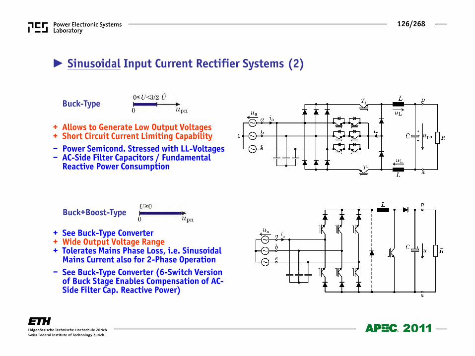
Boost-Type
Buck-Type
Buck+Boost-Type
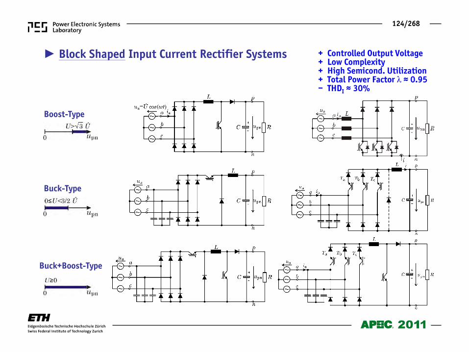
+ Controlled Output Voltage + Low Complexity + High Semicond. Utilization + Total Power Factor λ ≈ 0.95 – THDI ≈ 30%
Block Shaped Input Current Rectifier Systems
125/268
Boost-Type
Unregulated Output
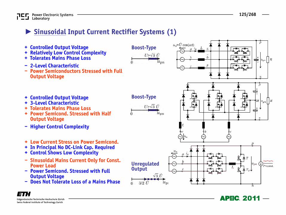
+ Controlled Output Voltage + Relatively Low Control Complexity + Tolerates Mains Phase Loss
– 2-Level Characteristic – Power Semiconductors Stressed with Full Output Voltage
+ Controlled Output Voltage + 3-Level Characteristic + Tolerates Mains Phase Loss + Power Semicond. Stressed with Half Output Voltage
– Higher Control Complexity
+ Low Current Stress on Power Semicond. + In Principal No DC-Link Cap. Required + Control Shows Low Complexity
– Sinusoidal Mains Current Only for Const. Power Load – Power Semicond. Stressed with Full Output Voltage – Does Not Tolerate Loss of a Mains Phase
Sinusoidal Input Current Rectifier Systems (1)
Boost-Type
126/268
Buck-Type
Buck+Boost-Type
+ Allows to Generate Low Output Voltages + Short Circuit Current Limiting Capability
– Power Semicond. Stressed with LL-Voltages – AC-Side Filter Capacitors / Fundamental Reactive Power Consumption
+ See Buck-Type Converter + Wide Output Voltage Range + Tolerates Mains Phase Loss, i.e. Sinusoidal Mains Current also for 2-Phase Operation
– See Buck-Type Converter (6-Switch Version of Buck Stage Enables Compensation of AC- Side Filter Cap. Reactive Power)
Sinusoidal Input Current Rectifier Systems (2)

127/268
Coffee Break !
128/268
Bidirectional PFC Rectifier Systems • Boost-Type Topologies • Buck-Type Topologies
129/268
Boost-Type Topologies
130/268
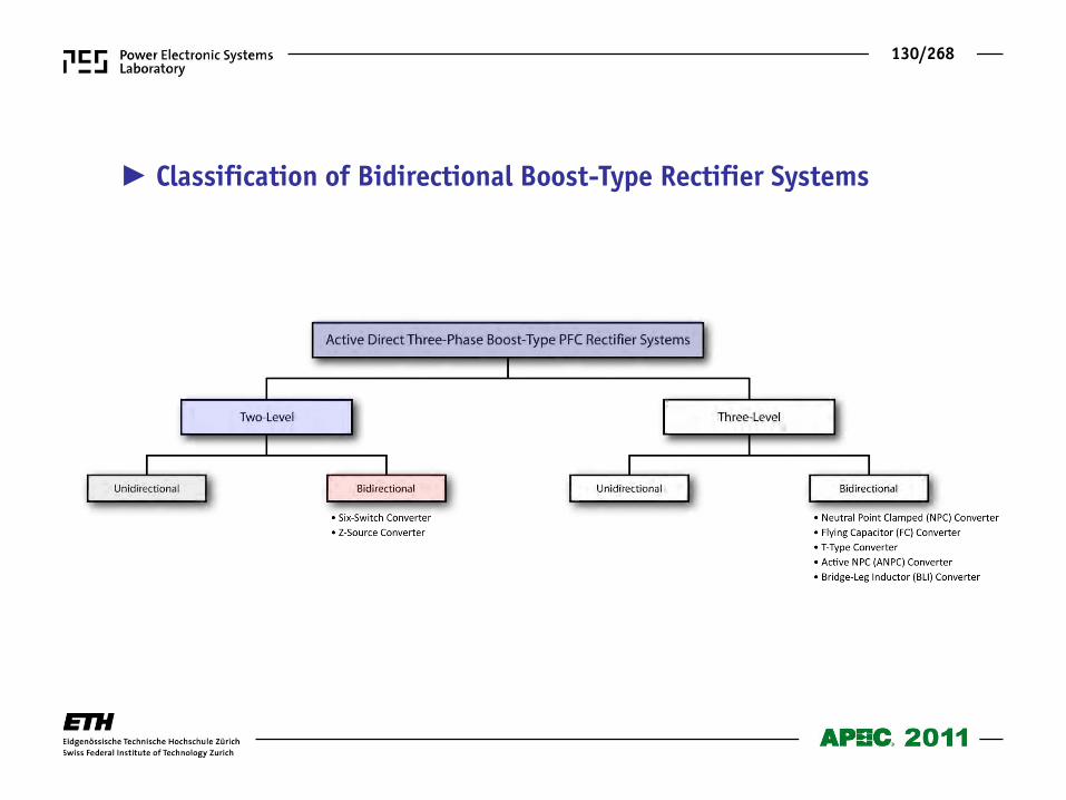
Classification of Bidirectional Boost-Type Rectifier Systems
131/268
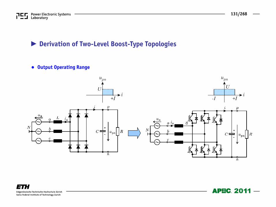
Derivation of Two-Level Boost-Type Topologies
Output Operating Range
132/268
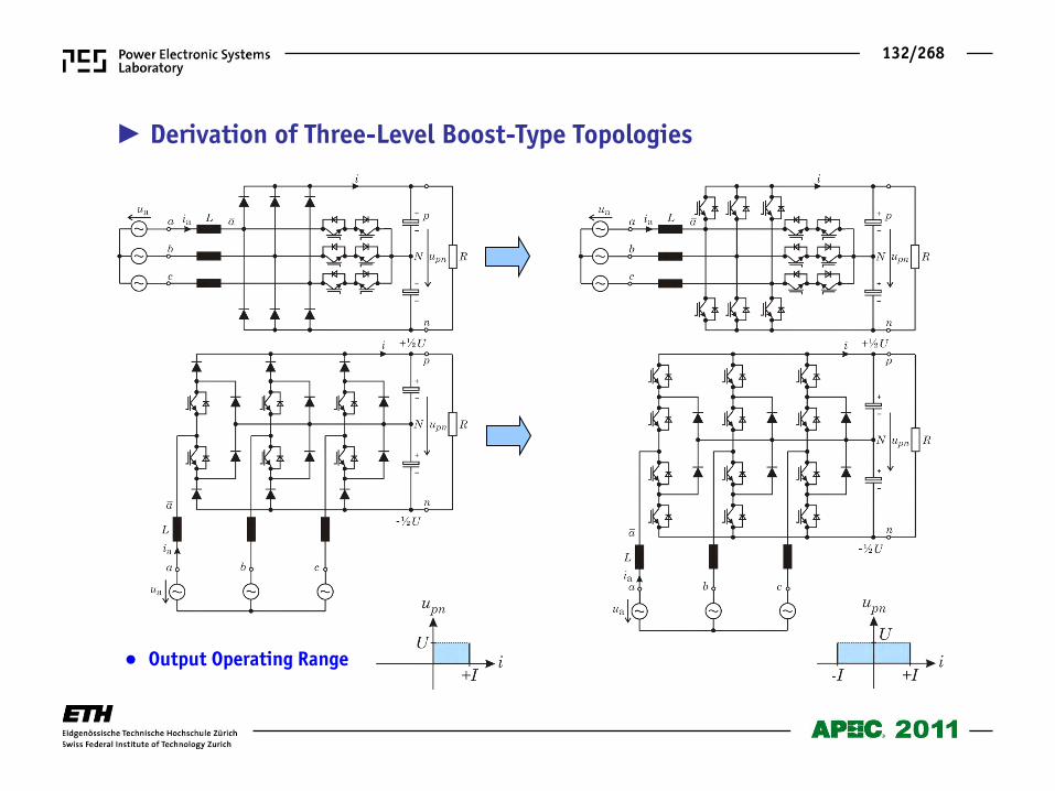
Derivation of Three-Level Boost-Type Topologies
Output Operating Range
133/268
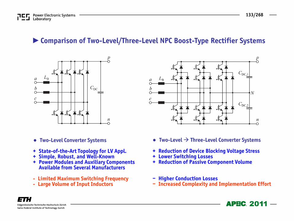
Two-Level Three-Level Converter Systems + Reduction of Device Blocking Voltage Stress + Lower Switching Losses + Reduction of Passive Component Volume – Higher Conduction Losses – Increased Complexity and Implementation Effort
+ State-of-the-Art Topology for LV Appl. + Simple, Robust, and Well-Known + Power Modules and Auxiliary Components Available from Several Manufacturers - Limited Maximum Switching Frequency - Large Volume of Input Inductors
Comparison of Two-Level/Three-Level NPC Boost-Type Rectifier Systems
Two-Level Converter Systems
134/268
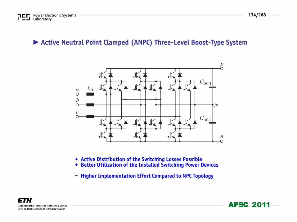
+ Active Distribution of the Switching Losses Possible + Better Utilization of the Installed Switching Power Devices – Higher Implementation Effort Compared to NPC Topology
Active Neutral Point Clamped (ANPC) Three-Level Boost-Type System
135/268
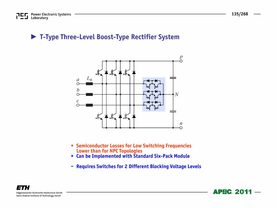
+ Semiconductor Losses for Low Switching Frequencies Lower than for NPC Topologies + Can be Implemented with Standard Six-Pack Module – Requires Switches for 2 Different Blocking Voltage Levels
T-Type Three-Level Boost-Type Rectifier System
136/268
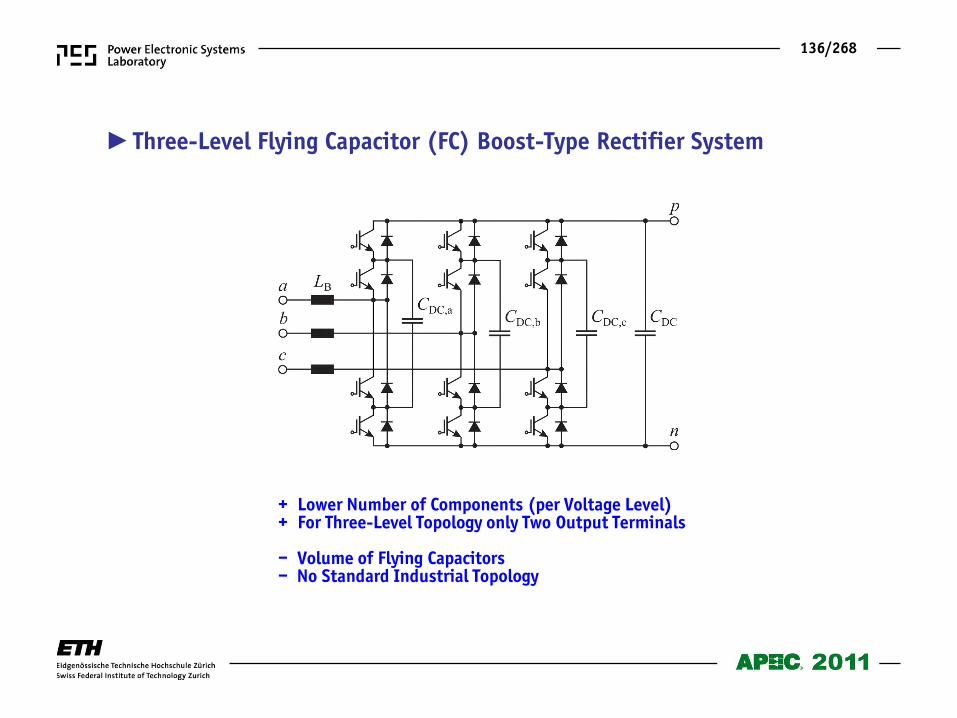
+ Lower Number of Components (per Voltage Level) + For Three-Level Topology only Two Output Terminals – Volume of Flying Capacitors – No Standard Industrial Topology
Three-Level Flying Capacitor (FC) Boost-Type Rectifier System
137/268
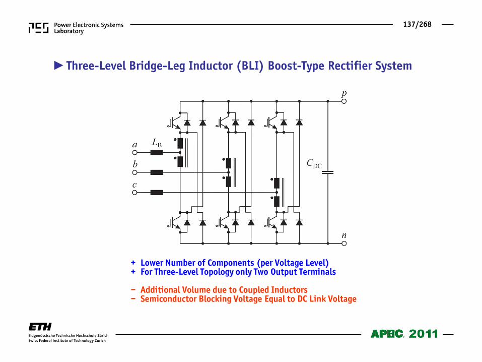
Three-Level Bridge-Leg Inductor (BLI) Boost-Type Rectifier System
+ Lower Number of Components (per Voltage Level) + For Three-Level Topology only Two Output Terminals – Additional Volume due to Coupled Inductors – Semiconductor Blocking Voltage Equal to DC Link Voltage
138/268
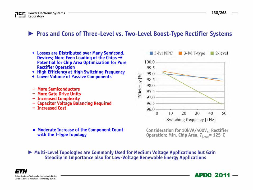
Multi-Level Topologies are Commonly Used for Medium Voltage Applications but Gain Steadily in Importance also for Low-Voltage Renewable Energy Applications
– More Semiconductors – More Gate Drive Units – Increased Complexity – Capacitor Voltage Balancing Required – Increased Cost
+ Losses are Distributed over Many Semicond. Devices; More Even Loading of the Chips Potential for Chip Area Optimization for Pure Rectifier Operation + High Efficiency at High Switching Frequency + Lower Volume of Passive Components
Moderate Increase of the Component Count with the T-Type Topology
Pros and Cons of Three-Level vs. Two-Level Boost-Type Rectifier Systems
Consideration for 10kVA/400VAC Rectifier Operation; Min. Chip Area, Tj,max= 125°C
139/268
Buck-Type Topologies
140/268
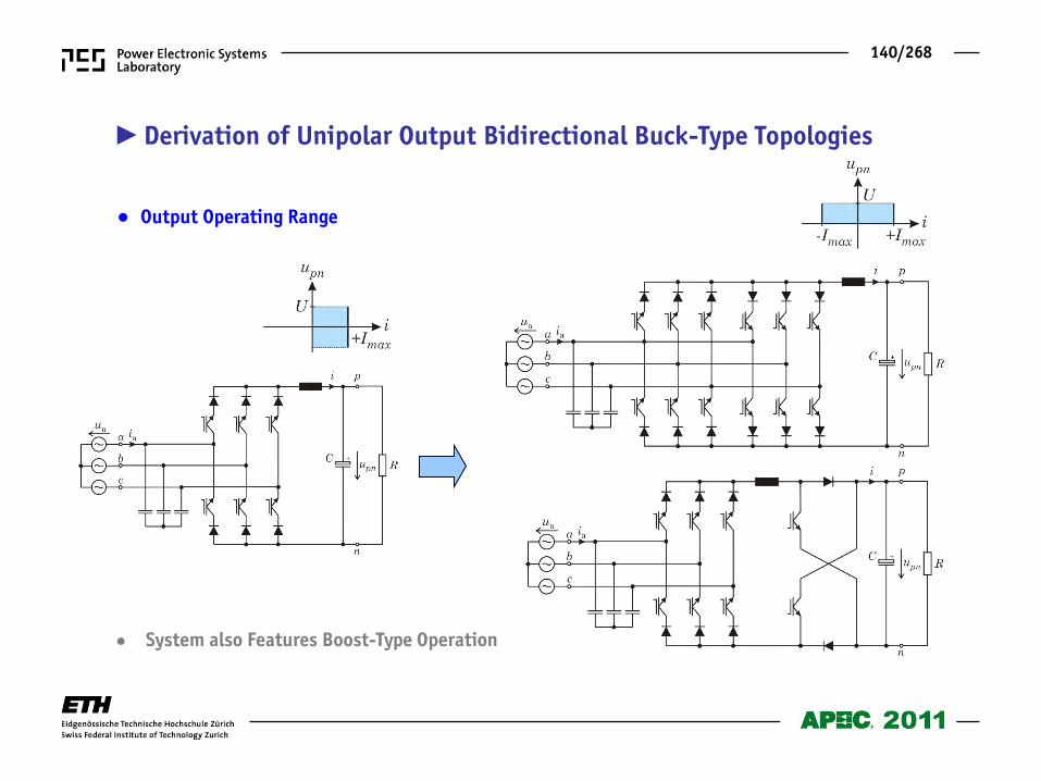
System also Features Boost-Type Operation
Output Operating Range
Derivation of Unipolar Output Bidirectional Buck-Type Topologies
141/268
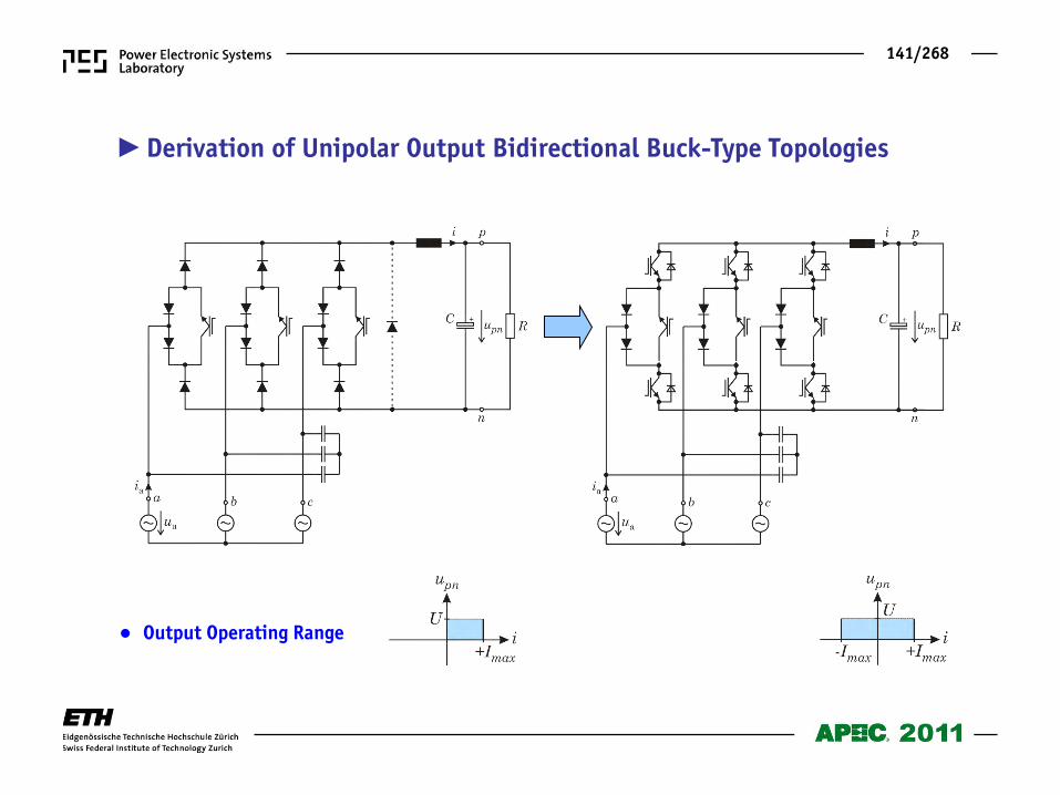
Derivation of Unipolar Output Bidirectional Buck-Type Topologies
Output Operating Range
142/268
End of Part 1
143/268
[1.1] P. Pejovic , "A Novel Low-Harmonic Three-Phase Rectifier," IEEE Transactions on Circuits and Systems I: Fundamental Theory and Applications, vol.49, no.7, pp.955-965, Jul 2002. [1.2] P. Pejovic, P. Bozovic, D. Shmilovitz, "Low-Harmonic, Three-Phase Rectifier That Applies Current Injection and a Passive Resistance Emulator,“ IEEE Power Electronics Letters , vol.3, no.3, pp. 96- 100, Sept. 2005. [1.3] P. Pejovic, Z. Janda, "Optimal Current Programming in Three-Phase High-Power-Factor Rectifier Based on Two Boost Converters," IEEE Transactions on Power Electronics, vol.13, no.6, pp.1152-1163, Nov 1998. [1.4] S. Kim, P. Enjeti, P. Packebush, and I. Pitel, “A New Approach to Improve Power Factor and Reduce Harmonics in a Three Phase Diode Rectifier Type Utility Interface,” Record of the IEEE Industry Applications Society Annual Meeting, Pt. II, pp. 993-1000, 1993. [1.5] P. Pejovic Z. Janda, “Low Harmonic Three-Phase Rectifiers Applying Current Injection,” Proc. of the Internat. Conf. on Power Electronics and Motion Control, Prague, 1998. [1.6] P. Pejovic and Z. Janda, “A Novel Harmonic-Free Three-Phase Diode Bridge Rectifier Applying Current Injection,” Proc. of the 14th IEEE Appl. Power Electron. Conf. APEC´99, Dallas, USA, March 14-18, Vol. 1, pp. 241-247, 1999. [1.7] P. Pejovic, and Z. Janda, “An Improved Current Injection Network for Three-Phase High-Power-Factor Rectifiers that Apply Third Harmonic Current Injection,” Letter to the Editor, IEEE Transactions on Industrial Electronics, Vol. 47, No. 2, pp. 497-499, 2000. [1.8] T. Sakkos and V. Sarv, “New Unity Power Factor Diode Rectifiers Using Ripple-Power Re-Rectification,” in. Proc. of the 8th Internat. Conf. on Power Electron. and Variable Speed Drives, London, Sept. 18-19, pp. 378-381, 2000. [1.9] T. Sakkos, V. Sarv, and J. Soojärv, “Optimun Diode-Switched Active Filters for Power Factor Correction of Single- and Three- Phase Diode Recifiers with Capacitive Smoothing,” in Proc. of the 7th European Conf. on Power Electron. and Appl., Trondheim, Norway, Vol. 2, pp. 870-875, 1997.
Passive Rectifier Systems
144/268
[2.1] H. Ertl, J.W. Kolar, and F.C. Zach, “A Constant Output Current Three-Phase Diode Bridge Employing a Novel Electronic Smoothing Inductor,” Proc. of the 40th Internat. Conf. on Power Conversion, Nuremberg, June 22-24, pp. 645–651 (1999). [2.2] K. Mino, M.L. Heldwein, and J.W. Kolar, "Ultra Compact Three-Phase Rectifier With Electronic Smoothing Inductor," Proc. of the 20th Annual IEEE Appl. Power Electron. Conf. and Exp. (APEC 2005), Vol.1, pp. 522-528 (2005). [2.3] R. Shimada, J.A. Wiik, T. Isobe, T. Takaku, N. Iwamuro, Y. Uchida, M. Molinas, T.M. Undeland, "A New AC Current Switch Called MERS with Low On-State Voltage IGBTs (1.54 V) for Renewable Energy and Power Saving Applications," Proc. of the 20th Internat. Symp. on Power Semicond. Devices and IC's, (ISPSD '08), pp.4-11, (2008 ). [2.4] T. Takaku, G. Homma, T. Isober, S. Igarashi, Y. Uchida, R. Shimada, "Improved Wind Power Conversion System Using Magnetic Energy Recovery Switch (MERS)," Proc. of the Industry Appl. Conf. 2005. 40th IAS Annual Meeting, Vol.3, pp. 2007- 2012 (2005). [2.5] J.A. Wiik, F.D. Widjaya, T. Isobe, T. Kitahara, R. Shimada, "Series Connected Power Flow Control using Magnetic Energy Recovery Switch (MERS)," Proc. of the Power Conv. Conf. - Nagoya, 2007 (PCC '07), pp.983-990 (2007). [2.6] J.A. Wiik, F.D. Wijaya, R. Shimada, "Characteristics of the Magnetic Energy Recovery Switch (MERS) as a Series FACTS Controller,“ IEEE Transactions on Power Delivery, vol.24, no.2, pp.828-836, (2009).
Hybrid Rectifier Systems (Electronic Reactance Based)
145/268
[2.7] H. Ertl, J.W. Kolar, and F.C. Zach, “A Constant Output Current Three-Phase Diode Bridge Employing a Novel Electronic Smoothing Inductor,” Proc. of the 40th Internat. Conf. on Power Conversion, Nuremberg, June 22-24, pp. 645–651 (1999). [2.8] S. Hansen, P.J. Enjeti, J.H. Hahn, and F. Blaabjerg, “An Integrated Single-Switch Approach to Improve Harmonic Performance of Standard PWM Adjustable Speed Drives,” Record of the 34th IEEE Industry Appl. Society Annual Meeting, Phoenix, USA, Oct. 3-7, Vol. 2, pp. 789–795 (1999). [2.9] A.M. El-Tamaly, P.N. Enjeti, and H.H. El-Tamaly, “An Improved Approach to Reduce Harmonics in the Utility Interface of Wind, Photovoltaic and Fuel Cell Power Systems,” Proc. of the 15th IEEE Appl. Power Electron. Conf., New Orleans, USA, Feb. 6-10, Vol. 2, pp. 1059–1065 (2000). [2.11] Z. Janda and P. Pejovic, “A High Power Factor Three-Phase Rectifier based on Adaptive Current Injection Applying Buck Converter,” Proc. of the 9th Internat. Conf. on Power Electron. and Motion Control, Kosice, Slovak Republic, Sept. 5-7, Vol. 3, pp. 140–144 (2000). [2.12] N. Mohan, “A Novel Approach to Minimize Line Current Harmonics in Interfacing Renewable Energy Sources with 3-Phase Utility Systems,” Proc. of the IEEE Appl. Power Electron. Conf., pp. 852–858 (1992). [2.13] S. Kim, P. Enjeti, D. Rendusara, and I.J. Pitel, “A New Method to Improve THD and Reduce Harmonics Generated by Three-Phase Diode Rectifier Type Utility Interface,” Record of the 29th IEEE Industry Appl. Society Annual Meeting, Denver, USA, Oct. 2-5, Vol. 2, pp. 1071–1077 (1994). [2.14] Y. Nishida, M. Nakaoka, Y. Ohgoe, and A. Maeda, “A Simple Three-Phase Boost-Mode PFC Rectifier,” Record of the 31st IEEE Industry Appl. Aociety Annual Meeting, San Diego, USA, Oct. 6-10, Vol. 2, pp. 1056–1060 (1996). [2.15] M. Rastogi, R. Naik, and N. Mohan, “Optimization of a Novel DC-Link Current Modulated Interface with 3-Phase Utility Systems to Minimize Line Current Harmonics,” Proc. of the Power Electron. Specialists Conf., Vol. I, pp. 162–167 (1992). [2.16] R. Naik, M. Rastogi, N. Mohan, R. Nilssen, C.P. Henze, “A Magnetic Device for Current Injection in a Three-Phase Sinusoidal Current Utility Interface,” Record of the IEEE Industry Appl. society Annual Meeting, Toronto, Canada, Oct. 2- 8, Pt. II, pp. 926–930 (1993). [2.17] M. Rastogi, R. Naik, and N. Mohan, “A Sinusoidal-Current Rectifier for Industrial and Distribution AC to DC Regulated DC Voltage,” Internat. Symp. on Electric Power Engin., Stockholm, Sweden, Pt.: Power Electronics, pp. 197–200 (1995). [2.18] Y. Nishida, “A New Simple Topology for Three-Phase Buck-Mode PFC,” Proc. of the 11th IEEE Appl. Power Electron. Conf., San Jose, USA, March 3-7, Vol. 2, pp. 531-537 (1996). [2.19] H. Kanaan, H.F. Blanchette, K. Al-Haddad, R. Chaffai, and L. Duguay, “Modeling and Analysis of a Three-Phase Unity Power Factor Current Injection Rectifier using One Loop Control Strategy,” Proc. of the 22nd IEEE Internat. Telecom. Energy Conf. Phoenix, USA, Sept. 10-14, pp. 518-525 (2000).
Hybrid Rectifier Systems (Active 3rd Harmonic Injection) (1)
146/268
Hybrid Rectifier Systems (Active 3rd Harmonic Injection) (2) [2.20] J.-I. Itoh, I. Ashida, "A Novel Three-Phase PFC Rectifier Using a Harmonic Current Injection Method," IEEE Transactions on Power Electronics, Vol.23, No.2, pp.715-722, March 2008. [2.21] H. Yoo, S.-K. Sul, „A Novel Approach to Reduce Line Harmonic Current for a Three-phase Diode Rectifier-fed Electrolytic Capacitor-less Inverter,“ Proc. of the IEEE Appl. Power Electronics Conf. and Exp. (APEC 2009), pp.1897-1903, 2009. [2.22] H. Yoo S.-K. Sul, "A New Circuit Design and Control to Reduce Input Harmonic Current for a Three-Phase AC Machine Drive System Having a very Small DC-link Capacitor,“ Proc. Of the 25th Ann. IEEE Appl. Power Electron. Conf. and Exp. (APEC 2010), pp.611-618, 2010. [2.23] L.R. Chaar, N. Mohan, and C.P. Henze, "Sinusoidal current rectification in a very wide range three-phase AC input to a regulated DC output," Proc. of the 30thIndust. Appl. Conf. (IAS '95), 8-12 Oct 1995, Vol.3, pp.2341-2347.
147/268
[2.23] A. Pietkiewicz and D. Tollik, “Three-Phase 7 kW Fan Cooled Telecom Rectifier with Active Power Factor Correction,” Proc. of the Internat. Telecom. Energy Conf., Paris, Vol. 1, pp. 407- 412 (1993). [2.24] A. Pietkiewicz and D. Tollik, “Cost/Performance Considerations for 3-Phase Input Current Shapers,” Proc. of the 1st Internat. Telecom. Energy Special Conf., Berlin, Germany, April 11-15, pp. 165-170 (1994). [2.25] N. Bäckman and H. Thorslund, “A New Light-Weight 100A/48V Three-Phase Rectifier,” Proc. of the Internat. Telecom. Energy Conference, pp. 92-97 (1991). [2.26] L.D. Salazar, P.D. Ziogas, and G. Joos, “On the Optimization of Switching Losses in DC-DC Boost Converters,” Proc. of the IEEE Applied Power Electron. Conf., pp. 703-708 (1992). [2.27] W.E. Rippel, “Optimizing Boost Chopper Charger Design,” IEEE Appl. Power Electron. Conf., Seminar 4: Electronic Power Factor Correction/Part 2 (1991). [2.28] J.C. Salmon, “A Variable Speed Drive Circuit Topology for Feeding a Three-Phase Inverter Bridge with Combined Current and Voltage DC Link,” Proc. of the 5th European Conf. on Power Electron. and Appl., Brighton, UK, Sept. 13-16, Vol. 5, pp. 139-144 (1993). [2.29] J.W. Kolar, H. Ertl, und F.C. Zach, “Realization Considerations for Unidirectional Three-Phase PWM Rectifier Systems with Low Effects on the Mains,” Proc. of the 6th Internat. Conf. on Power Electron. and Motion Control, Budapest, Oct. 1-3, Vol. 2, pp. 560 - 565 (1990). [2.30] M.E. Jacobs, R.W. Farrington, G.H. Fasullo, Y. Jiang, R.J. Murphy, V.J. Thottuvelil, and K.J. Timm “An Improved High-Efficiency Rectifier for Telecom Applications,” Proc. of the 18th Internat. Telecom. Energy Conf., Oct. 6-10, Boston, USA, pp. 530-535 (1996). [2.31] J. Salmon, “PWM Inverter Harmonic Correction Topologies for Three-Phase Diode Rectifiers,” Proc. of the 8th Intern. Conf. on Power Electron. and Variable Speed Drives, London, Sept. 18-19, pp. 299-304 (2000).
Hybrid Rectifier Systems (Combination of Diode Bridge and DC/DC Converter)
148/268
[2.32] S. Masukawa and S. Iida, “An Improved Three-Phase Diode Rectifier for Reducing AC Line Current Harmonics,” in Proc. of the European Conf. on Power Electronics and Applications, Trondheim, Norway, Vol. 4, pp. 227–232, 1997. [2.33] C. Sewan, S.L. Bang, and P.N. Enjeti, ”New 24-Pulse Diode Rectifier System for Utility Interface of High-Power AC Motor Drives,” IEEE Trans. On Ind. Applications, Vol. 32, No. 2, pp. 531–541, 1997. [2.34] K. Oguchi, H. Hama, and T. Kubota, “Line-Side Reactor-Coupled Double Voltage-Fed Converter System with Ripple-Voltage Injection,” Record of the 29th IEEE Power Electr. Specialists Conf., Fukuoka, Japan, Vol. 1, pp. 753–757, 1998. [2.35] J. Kikuchi, M.D. Manjrekar, and T.A. Lipo, “Performance Improvement of Half Controlled Three-Phase PWM Boost Rectifier,” Proceedings of the 30th IEEE Power Electronics Specialists Conf., Charleston (SC), Vol. 1, pp. 319–324, 1999. [2.36] C.A. Munoz, I. Barbi, “A New High-Power-Factor Three-Phase AC-DC Converter: Analysis Design, and Experimentation,” IEEE Transactions on Power Electronics, Vol. 14, No. 1, pp. 90–97, 1999. [2.37] K. Oguchi, G. Maeda, N. Hoshi, and T. Kubota, “Voltage-Phase Shifting Effect of Three-Phase Harmonic Canceling Reactors and Their Applications to Three-Level Diode Rectifiers,” Record of the 34th IEEE Ind. Appl. Society Annual Meeting, Phoenix (AZ), Vol. 2, pp. 796–803, 1999. [2.38] G.R. Kamath, B. Runyan, and R. Wood, “A Compact Auto-Transformer-Based 12-Pulse Rectifier Circuit,” in Proc. of the 27th Annual Conf. of the Ind. Electr. Society, Denver (CO), Vol. 2, pp. 1344–1349, 2001. [2.39] D.J. Perreault, and V. Caliskan, “Automotive Power Generation and Control,” IEEE Transactions on Power Electronics, Vol. 19, No. 3, pp. 618–630, 2004. [2.40] S. Choi, “A Three-Phase Unity-Power-Factor Diode Rectifier with Active Input Current Shaping,” IEEE Transactions on Ind. Electronics, Vol. 52, No. 6, pp. 1711–1714, 2005. [2.41] F. J. Chivite-Zabalza, “High Power Factor Rectification for Aerospace Systems,” Ph.D. Thesis, The Univ. of Manchester, 2006.
Hybrid Rectifier Systems (Multi-Pulse / Half Controlled Rectifier Systems)
149/268
Phase Modular Y-Rectifier (1) [3.1] D. Gauger,T. Froeschle, L. Illingworth, and E. Rhyne, “A Three-Phase Off-Line Switching Power Supply with Unity
Power Factor and Low TIF,” Proceedings of the International Telecommunications Energy Conference, Toronto, Oct. 19-22, pp. 115-121,1986.
[3.2] R.A. Langley, J.D. van Wyk, J.J. Schoeman, “A High Technology Battery Charging System for Railway Signaling Applications,” Proceedings of the 3rd European Conference on Power Electronics and Applications, Aachen, Germany, Vol. III, pp. 1433- 1434, 1989.
[3.3] D. Chapman, D. James, and C.J. Tuck, “A High Density 48V 200A Rectifier with Power Factor Correction – An Engineering Overview,” Proceedings of the IEEE International Telecommunications Energy Conference, Paris, France, Vol. 1, pp. 118-125, 1993.
[3.4] S.Y.R Hui, and H. Chung, “Paralleling Power Converters for AC-DC Step-Down Power Conversion with Inherent Power Factor Correction,” Proceedings of the 7th European Conference on Power Electronics and Applications, Trondheim, Norway, Vol. 1, pp. 1.182-1.187, 1997.
[3.5] D. S. L. Simonetti, J. Sebastian, and J. Uceda, “The Discontinuous Conduction Mode Sepic and Cuk Power Factor Preregulators: Analysis and Design,” in IEEE Transactions on Industrial Electronics, Vol. 44, No. 5, pp. 630-637, 1997.
[3.6] S.Y.R Hui, H. Chung, Y.K.E. Ho, and Y.S. Lee, “Modular Development of Single-Stage 3-Phase PFC using Single-Phase Step-Down Converters,” Record of the 29th IEEE Power Electronics Specialists Conference, Fukuoka, Japan, May 17-22, Vol. 1, pp. 776-782, 1998.
[3.7] M.A. de Rooij, J.A. Ferreira, and J.D. van Wyk, “A Three-Phase Soft-Switching Transformer Isolated Unity Power Factor Front End Converter,” Record of the 29th IEEE Power Electronics Specialists Conference, Fukuoka, Japan, May 17-22, Vol. 1, pp. 798-804, 1998.
[3.8] M. Karlsson, C. Thoren, and T. Wolpert, “A Novel Approach to the Design of Three-Phase AC/DC Power Converters with Unity Power Factor,” Proceedings of the 21st IEEE International Telecommunications Energy Conference, Copenhagen, Denmark, June 6-9, paper no. 5-1,1999.
[3.9] M.L. Heldwein, A.F. de Souza, and I. Barbi, ”A Simple Control Strategy Applied to Three-Phase Rectifier Units for Telecommunication Applications using Single-Phase Rectifier Modules,” Proceedings of the 30th IEEE Power Electronics Specialists Conference, Charleston (SC), USA, Vol.2, pp. 795-800, 1999.
[3.10] Y.K.E. Ho, S.Y.R. Hui, and Y.S. Lee, “Characterization of Single-Stage 3-Phase Power Factor Correction Circuit Using Modular Single-Phase PWM DC-to-DC Converters,” Proceedings of the 30th IEEE Power Electronics Specialists Conference, Charleston (SC), USA, Vol.2, pp. 704-708, 1999.
150/268
[3.11] Y.K.E. Ho, S.Y.R. Hui, and Y.S. Lee, ”Characterization of Single-Stage Three-Phase Power-Factor-Correction Circuit Using Modular Single-Phase PWM DC-to-DC Converters,” IEEE Transactions on Power Electronics, Vol. 15, No. 1, pp. 62-71, 2000. [3.12] R. Greul, U. Drofenik, and J.W. Kolar, “Analysis and Comparative Evaluation of a Three-Level Unity Power Factor Y-Rectifier“, in Proc. 25th International Telecommunications Energy Conference INTELEC 2003, pp. 421–428, 2003. [3.13] J. Biela, U. Drofenik, F. Krenn, J. Miniböck, and J.W. Kolar, “Novel Three-Phase Y-Rectifier Cyclic 2 Out of 3 DC Output Voltage Balancing”, in Proc. 29th International Telecommunications Energy Conference INTELEC 2007, pp. 677–685, 2007. [3.14] R. Greul, S.D. Round, J.W. Kolar, “Analysis and Control of a Three-Phase Unity Power Factor Y-Rectifier”, IEEE Trans. Power Electron., vol. 22, no. 5, pp. 1900–1911, Sept. 2007.
Phase Modular Y-Rectifier (2)
151/268
Phase Modular -Rectifier [3.15] M.J. Kocher, and R.L. Steigerwald, “An AC-to-DC Converter with High Quality Input Waveforms,” IEEE Transactions
on Industry Applications”, Vol. IA-19, No. 4, pp. 586-599, 1983. [3.16] S.A. El-Hammamsy, “Coupled Inductor Rectification and Cycloconversion,” Proceedings of the 3rd IEEE Applied
Power Electronics Conference, Feb. 1-5, New Orleans, USA, pp. 258-266, 1988. [3.17] R. Ridley, S. Kern, and B. Fuld, “Analysis of a Wide Input Range Power Factor Correction Circuit for Three-Phase
Applications,” Proceedings of the IEEE Applied Power Electronics Conference, pp. 299-305, 1993. [3.18] B. Fuld, S. Kern, and R.A. Ridley, “Combined Buck and Boost Power Factor Controller for Three-Phase Input,”
Proceedings of the 5th European Conference on Power Electronics and Applications, Brighton, UK, Vol. 7, pp. 144-148, 1993.
[3.19] D. York, E. Filer, and K. Haliburton, “A Three-Phase Input Power Processing Unit with Unity Power Factor and Regulated DC Output,” Proceedings of the High Frequency Power Conversion Conference, pp. 349-356, 1994.
[3.20] A.-Ch. Rufer and Ch.-B. Andrianirina, “A Symmetrical 3 Phase-2 Switch PFC-Power Supply for Variable Output Voltage,” Proceedings of the 6th European Conference on Power Electronics and Applications, Sevilla, Spain, Sept. 19-21, Vol. 3, pp. 3.254-3.258, 1995.
[3.21] E.S. de Andrade, D.C. Martins, and I. Barbi, “Isolated Three-Phase Rectifier Unit with High Power Factor”, Proceedings of the 18th IEEE International Telecommunications Energy Conference, Boston, USA, Oct. 6-10, pp. 536-542, 1996.
[3.22] M. Tognolini, M., and A.-Ch. Rufer, “A DSP-Based Control for a Symmetrical Three-Phase Two-Switch PFC-Power Supply for Variable Output Voltage,” Proceedings of the 27th IEEE Power Electronics Specialists Conference, Baveno, Italy, June 23-27, Vol. II, pp. 1588-1594, 1996.
[3.23] R. Ayyanar, et al., “Single-Stage Power-Factor-Correction Circuit Using Three Isolated Single-Phase SEPIC Converters Operating in CCM,” Records of 2000 IEEE PESC, 2000.
[3.24] J.W. Kolar, F. Stögerer, Y. Nishida, “Evaluation of a Delta-Connection of Three Single-Phase Unity Power Factor Rectifier Systems (-Rectifier) in Comparison to a Direct Three-Phase Realization, Part I –Modulation Schemes and Input Current Ripple”, in Proc. 7th European Power Quality Conference, pp. 101–108, 2001.
[3.25] R. Greul, “Modulare Dreiphasen-Pulsgleichrichtersysteme“, Ph.D. Thesis, Eidgenössische Technische Hochschule – ETH Zürich, Switzerland, 2006.
[3.26] R. Greul, S.D. Round, J.W. Kolar, “The Delta-Rectifier: Analysis, Control and Operation“, IEEE Trans. Power Electron., vol. 21, no. 6, pp. 1637–1648, Nov. 2006.
152/268
Direct Three-Phase Active PFC Converter (Boost-Type DCM Converters) [4.1] A. R. Prasad et al., “An Active Power Factor Correction Technique for Three-Phase Diode Rectifiers,” IEEE Transactions on Power Electronics, Vol. 6, No. 1, pp. 83-92, 1991. [4.2] J.W. Kolar et al, “Space Vector-Based Analytical Analysis of the Input Current Distortion of a Three-Phase Discontinuous- Mode Boost Rectifier System,” in IEEE PESC’93 Records, pp. 696-703. [4.3] J.W. Kolar, et al., “A Comprehensive Design Approach for a Three-Phase High-Frequency Single-Switch Discontinuous-Mode Boost Power Factor Corrector based on Analyticaly Derived Normalized Converter Component Ratings,” IEEE Transactions on Industry Applications, Vol. 31, No. 3, 1995, pp. 569-582. [4.4] J. Sun, et al., “Harmonic reduction techniques for single-switch three-phase boost rectifiers,” IAS’96, pp. 1225-1232. [4.5] Y. Jang and M.M. Jovanovic, “A comparative study of single-switch, three-phase, high-power-factor rectifiers,” Proc. Of the IEEE Appl. Power Electronics Conf. (APEC’98), 1093-1099. [4.6] S. Gataric, et al., “Soft-switched single-switch three-phase rectifier with power factor correction,” in Proceedings of IEEE Appl. Power Electron. Conf. (APEC’94), pp. 738-744. [4.7] E. H. Ismail, “A low-distortion three-phase multiresonant boost rectifier with zero-current switching,” IEEE Transactions on Power Electronics, Vol. 13, No. 4, pp. 718-726, 1998. [4.8] H. Oishi et al., “Sepic-derived three-phase sinusoidal rectifier operating in discontinuous current conduction mode,” in IEE Proceedings – Electric Power Applications, Vol. 142, No. 4, pp. 239-245, 1995. [4.9] L. Malesani et al., “Three-Phase Power Factor Controller with Minimum Output Voltage Distortion,” in Proceedings of INTELEC’93, pp. 463-468. [4.10] D. M. Xu, C. Yang, J. H. Kong, and Z. Qian, “Quasi Soft-Switching Partly Decoupled Three-Phase PFC with Approximate Unity Power Factor,” In Proc. of the Appl. Power Electron. Conf. (APEC’98), pp. 953-957. [4.11] P. Barbosa, F. Canales, J.-C. Crebier, F.C. Lee, "Interleaved three-phase boost rectifiers operated in the discontinuous conduction mode: analysis, design considerations and experimentation," IEEE Transactions on Power Electronics, Vol.16, No.5, pp.724-734, Sep 2001. [4.12] P. Barbosa, F. Canales, F. Lee, "Analysis and evaluation of the two-switch three-level boost rectifier," Proc. of the 32nd
Annual IEEE Power Electronics Specialists Conf. (PESC 2001), Vol. 3, pp.1659-1664, 2001.
153/268
[5.1] J.W. Kolar, H. Ertl, F.C. Zach, “Realization Considerations for Unidirectional Three-Phase PWM Rectifier Systems with low Effects on the Mains,” Proc. of the 6th Int. Conf. on Power Electronics and Motion (PEMC 1990), Budapest. [5.2] M. Hartmann, J. Miniboeck, J.W. Kolar, “A Three-Phase Delta Switch Rectifier for More Electric Aircraft Applications Employing a Novel PWM Current Control Concept,” Proc. of 24th Annual IEEE Applied Power Electron. Conf. and Exp. (APEC 2009), 15-19 Feb. 2009, pp.1633-1640. [5.3] S.K.T. Miller, J. Sun, “Comparative study of three-phase PWM rectifiers for wind energy conversion,” Proc. of the 21th Annual IEEE Applied 12 Power Electronics Conference and Exposition (APEC ’06), 19-23 March 2006, pp.937-943. [5.4] J.C. Salmon, “Reliable 3-phase PWM Boost Rectifiers Employing a Stacked Dual Boost Converter Subtopology,” IEEE Transactions on Industry Applications, Vol. 32, No. 3, pp.542-551, 1996. [5.5] I. Barbi, J.C. Fagundes, and C.M.T Cruz, “A Low Cost High Power Factor Three-Phase Diode Rectifier with Capacitive Load,” Proc. of the IEEE Appl. Power Electron. Conf., Vol. 2, pp. 745-751 (1994). [5.6] W. Koczara, and P. Bialoskorski, “Modified Rectifiers with Unity Power Factor,” Proc. of the Internat. Conf. on Power Electron. and Motion Control,” Warsaw, Poland, Sept. 20-22, Vol. 1, pp. 309-314 (1994). [5.7] J. Spanicek, and D. Platt, “Minimal Circuit for Power System Conditioning,” Proc. of the Internat. Conf. on Power Electronics and Drive Systems, Singapore, Feb. 21-24, Vol. 1, pp. 543-548 (1995). [5.8] F. Lafitte, B. Dakyo, L. Protin, and Koczara, W, “Three-Phase Sinusoidal Current Absorption AC-DC Converter for High Power Supply for Telecommunication,” Proc. of the 17th IEEE Internat. Telecom. Energy Conf., The Hague, The Netherlands, Oct. 29-Nov. 1, pp. 715-720 (1995). [5.9] D. Carlton, W.G. Dunford, M. Edmunds, “Continuous Conduction Mode Operation of a Three-Phase Power Factor Correction Circuit with Quasi Tridirectional Switches,” Proc. of the 30th Annual IEEE Power Electronics Specialists Conf. (PESC 99), Aug 1999, vol.1, pp.205-210. [5.10] A. Lima, C. Cruz, F. Antunes, “A new low cost AC-DC Converter with High Input Power Factor,” Proc. of the 22nd IEEE Internat. Conf. on Indust. Electron., Control, and Instrumentation (IECON’96), 5-10 Aug 1996, Vol.3, pp.1808-1813. [5.11] C. Qiao, K.M. Smedley, “A General Three-Phase PFC Controller for Rectifiers with a Parallel-Connected Dual Boost Topology,” IEEE Transactions on Power Electronics, Vol.17, No.6, Nov 2002, pp. 925-934. [5.12] N. Noor, J. Ewanchuk, J.C. Salmon, “PWM Current Controllers for a Family of 3-Switch Utility Rectifier Topologies,” Proc. of the Canadian Conference on Electrical and Computer Engineering (CCECE2007), 22-26 April 2007, pp.1141-1144. [5.13] J.C. Salmon, “Comparative Evaluation of Circuit Topologies for 1-Phase and 3-Phase Boost Rectifiers Operated with a Low Current Distortion,” Proc. of Canadian Conference on Electrical and Computer Engineering, Halifax, NS, Canada (1994), 25-28 Sep. 1994, Vol.1, pp. 30-33.
Direct Active Three-Phase PFC Rectifier Systems (Two-Level CCM Boost-Type) (1)
154/268
[5.14] J.C. Salmon, “Comparative Evaluation of Circuit Topologies for 1-Phase and 3-Phase Boost Rectifiers Operated with a Low Current Distortion,” Proc. of Canadian Conference on Electrical and Computer Engineering, Halifax, NS, Canada (1994), 25-28 Sep. 1994, Vol.1, pp. 30-33. [5.15] D. Carlton, W.G. Dunford, M. Edmunds, "Harmonic Reduction in the 3-Phase 3-Switches Boost-Delta Power Factor Correction Circuit Operating in Discontinuous Conduction mode," 20th Internat. Telecom. Energy Conf. (INTELEC 1998), pp.483-490. [5.16] Tao Lei, Xiao-Bin Zhang, Yan-Jun Dong, Jing-Hui Zhao, Hui Lin, "Study of High Power Factor Rectifiers Based on One Cycle Control in Aircraft Electric Power System," 12th Internat. Middle East Power System Conf. (MEPCON 2008), pp.325- 329. [5.17] C.L. Chen, “A new Space-Vector-Modulated Control for a Unidirectional Three-Phase Switch-Mode Rectifier,” IEEE Transactions on Industrial Electronics, Vol.45, No.2, Apr 1998, pp.256-262. [5.18] W. Koczara, “Unity Power Factor Three-Phase Rectifier,” Proc. of the Internat. Power Quality Conf., Munich, pp. 79-88 (1992). [5.19] W. Koczara and P. Bialoskorski, “Controllability of the Simple Three-Phase Rectifier Operating with Unity Power Factor,” Proc. of the 5th European Conf. on Power Electron. and Appl., Brighton, UK, Vol. 7, pp. 183-187 (1993). [5.20] G. Spiazzi and F. C. Lee, “Implementation of Single-Phase Boost Power Factor Correction Circuits in Three-Phase Applications,” Proc. of the IEEE IECON’94, pp. 250-255 (1994). [5.20] B. Singh, B.N. Singh, A. Chandra, K. Al-Haddad, A. Pandey, D.P. Kothari, "A review of three-phase improved power quality AC-DC converters," Industrial Electronics, IEEE Transactions on , vol.51, no.3, pp. 641- 660, June 2004. [5.21] J.W. Kolar, H. Ertl, "Status of the techniques of three-phase rectifier systems with low effects on the mains," Proc.of the 21st Internat. Telecom. Energy Conf. (INTELEC '99), pp.16 pp., Jun 1999.
Direct Active Three-Phase PFC Rectifier Systems (Two-Level CCM Boost-Type) (2)
155/268
[6.1] E.L.M. Mehl and I. Barbi, “Design Oriented Analysis of a High Power Factor and Low Cost Three-Phase Rectifier,” Proc. of the 27th IEEE Power Electron. Specialists Conf., Baveno, Italy, June 23-27, Vol. I, pp. 165-170 (1996). [6.2] F. Daniel, R. Chaffai, and K. Al-Haddad, “Three-Phase Diode Rectifier with Low Harmonic Distortion to Feed Capacitive Loads,” Proc. of the 11th IEEE Appl. Power Electron. Conf., San Jose, USA, March 3-7, Vol. 2, pp. 932-938 (1996). [6.3] F. Daniel, R. Chaffai, K. Al-Haddad, and R. Parimelalagan, “A New Modulation Technique for Reducing the Input Current Harmonics of a Three-Phase Diode Rectifier with Capacitive Load,” IEEE Transactions on Industry Applications, Vol. 33, No. 5, pp. 1185-1193 (1997). [6.4] K. Oguchi, T. Yoshizawa, N. Hoshi, and T. Kubota, “Programmed Pulse Width Modulation of Three-Phase Three-Level Diode Rectifiers,” Proc. of the 9th Internat. Conf. on Power Electron. and Motion Control, Kosice, Slovak Republic, Sept. 5-7, Vol. 3, pp. 102-107 (2000). [6.5] Y. Zhao, Y. Li, and T.A. Lipo, “Force Commutated Three-Level Boost Type Rectifier,” Record of the IEEE Industry Appl. Society Annual Meeting, Toronto, Canada, Vol. II, pp. 771-777 (1993). [6.6] J.W. Kolar and F.C. Zach, “A Novel Three-Phase Three-Switch Three-Level Unity Power Factor PWM Rectifier,” Proc. of the 28th Internat. Power Conv. Conf., Nürnberg, 28. bis 30. Juni, S. 125 - 138 (1994). [6.7] J.W. Kolar and F.C. Zach, “A Novel Three-Phase Utility Interface Minimizing Line Current Harmonics of High-Power Telecommunications Rectifier Modules,” Proc. of the 16th IEEE Internat. Telecom. Energy Conf., Vancouver, Canada, Oct. 30-Nov. 3, pp. 367 - 374 (1994). [6.8] J.W. Kolar, U. Drofenik, and F.C. Zach, “Space Vector Based Analysis of the Variation and Control of the Neutral Point Potential of Hysteresis Current Controlled Three-Phase/Switch/Level PWM Rectifier Systems,” Proc. of the Internat. Conf. on Power Electronics and Drive Systems, Singapore, Feb. 21-24, Vol. 1, pp. 22 - 33 (1995). [6.9] J.W. Kolar, U. Drofenik, and F.C. Zach, “Current Handling Capability of the Neutral Point of a Three-Phase/Switch/Level Boost-Type PWM (VIENNA) Rectifier,” Proc. of the 28th IEEE Power Electronics Conf., Baveno, Italy, June 24-27, Vol. II, pp. 1329 - 1336 (1996). [6.10] J.W. Kolar, U. Drofenik and F.C. Zach, “On the Interdependence of AC-Side and DC-Side Optimum Control of Three-Phase Neutral-Point-Clamped (Three-Level) PWM Rectifier Systems,” Invited Paper, Proceedings of the 7th Internat. Power Electronics and Motion Control Conf., Budapest, Hungary, Sept. 2-4, Vol. 1, pp. 40 - 49 (1996). [6.11] J.W. Kolar, H. Sree, U. Drofenik, N. Mohan, and F.C. Zach, ”A Novel Three-Phase Three-Switch Three-Level High Power Factor SEPIC-Type AC-to-DC Converter,” Proc. of the 12th IEEE Appl. Power Electron. Conf., Atlanta, Feb. 23-27, Vol. 2, pp. 657 - 665 (1997).
Direct Active Three-Phase PFC Rectifier Systems (Three-Level CCM Boost-Type) (1)
156/268
[6.12] U. Drofenik, R. Windauer, J.W. Kolar, E. Masada, and F.C. Zach, “Analysis and Comparison of Different Input Current Control Schemes for a Three-Phase/Switch/Level Boost-Type (VIENNA) Rectifier,” Proc. of the 1st Internat. Congress on Energy, Power & Motion Control, Tel Aviv, Israel, May 5-6, pp. 35 - 41 (1997). [6.13] J.W. Kolar and U. Drofenik, “A New Switching Loss Reduced Discontinuous PWM Scheme for a Unidirectional Three- Phase/Switch/Level Boost-Type PWM (VIENNA) Rectifier,” Proc. of the 21st IEEE Internat. Telecom. Energy Conf., Copenhagen, Denmark, June 6-9, Paper No. 29-2 (1999). [6.14] U. Drofenik, and J.W. Kolar, “Comparison of Not Synchronized Sawtooth Carrier and Synchronized Triangular Carrier Phase Current Control for the VIENNA Rectifier I,” Record of the IEEE Internat. Symp. on Industr. Electronics, Bled, Slovenia, June 12-16, Vol. 1, pp. 13 - 19 (1999). [6.15] U. Drofenik and J.W. Kolar, “Influence of the Current-Dependency of the Inductance of the Input Inductors of Three- Phase PWM Rectifier Systems on the Modulation Scheme being Optimal Concerning the Mains Current Ripple RMS Value,” Proc. of the International Power Electronics Conference, Tokyo, April 3-7, Vol. 2, pp. 1017 - 1022 (2000). [6.16] J.W. Kolar, F. Stögerer, J. Miniböck, and H. Ertl, “A Novel Concept for Reconstruction of the Input Phase Currents of a Three-Phase/Switch/Level PWM (VIENNA) Rectifier Based on Neutral Point Current Measurement,” Proc. of the 31st IEEE Power Electronics Specialists Conf., Galway, Ireland, June 18-23, pp. 139 - 146 (2000). [6.17] J. Miniböck, F. Stögerer and J.W. Kolar, “A Novel Concept for Mains Voltage Proportional Input Current Shaping of a CCM Three-Phase PWM Rectifier Eliminating Controller Multipliers I. Basic Theoretical Considerations and Experimental Verification,“ Proc. of the 16th Annual IEEE Appl. Power Electronics Conf. and Exp. (APEC 2001), Vol.1, pp.582-586 vol.1, 2001. [6.18] J. Miniböck, and J.W. Kolar, “Comparative Theoretical and Experimental Evaluation of Bridge Leg Topologies of a Three- Phase/Switch/Level PWM (VIENNA) Rectifier,” Proc. of the 32nd Annual Power Electronics Specialists Conference, (PESC. 2001) Vol.3, no., pp.1641-1646 vol. 3, 2001. [6.19] F. Stogerer, J. Minibock, J.W. Kolar, "Implementation of a Novel Control Concept for Reliable Operation of a VIENNA Rectifier Under Heavily Unbalanced Mains Voltage Conditions," 32nd Annual Power Electronics Specialists Conference, (PESC. 2001), Vol.3, pp.1333-1338, 2001. [6.20] C. Qiao, and K.M. Smedley, “Three-Phase Unity-Power-Factor VIENNA Rectifier with Unified Constant Frequency Integration Control,” Proc. of the IEEE Internat. Power Electronics Congress, Acapulco, Mexico, Oct. 15-19, pp. 125-130 (2000). [6.21] C. Qiao, and K.M. Smedley, “A General Three-Phase PFC Controller – Part II. for Rectifiers with Series-Connected Dual- Boost Topology,” Record of the 34th IEEE Industry Applications Society Annual Meeting, Phoenix, USA, Oct. 3-7, Vol. 4, pp. 2512-2519 (1999).
Direct Active Three-Phase PFC Rectifier Systems (Three-Level CCM Boost-Type) (2)
157/268
[6.22] M.L. Heldwein, S.A. Mussa, I. Barbi, "Three-Phase Multilevel PWM Rectifiers Based on Conventional Bidirectional Converters," IEEE Transactions on Power Electronics, Vol.25, No.3, pp.545-549, March 2010. [6.23] P. Ide, N. Froehleke, and H. Grotstollen, “Comparison of Selected 3-Phase Switched Mode Rectifiers,” Proc. of the 19th IEEE Internat. Telecom. Energy Conf., Melbourne, Australia, Oct. 19-23, pp. 630-636 (1997). [6.24] P. Ide, N. Froehleke, N. and H. Grotstollen, “Investigation of Low Cost Control Schemes for a Selected 3-Level Switched Mode Rectifier,” Proc. of the 19th IEEE Internat. Telecom. Energy Conference, Melbourne, Australia, Oct. 19-23, pp. 413-418 (1997). [6.25] P. Ide, N. Froehleke, H. Grotstollen, W. Korb, and B. Margaritis, “Analysis of Three-Phase/Three-Level Rectifiers at Low Load and Discontinuous Conduction Mode,” Proc. of the IEEE Applied Power Electronics Conf., New Orleans, USA, Feb. 6- 10, Vol. 1, pp. 197-204 (2000). [6.26] P. Ide, N. Froehleke, H. Grotstollen, W. Korb, and B. Margaritis, “Operation of a Three-Phase/Three-Level Rectifier in Wide Range and Single-Phase Applications,” Proc. of the 25th Annual Conf. of the Industrial Electronics Society (IECON), San Jose, USA, Nov. 29 - Dec. 3, pp. 577-582 (1999). [6.27] W. Koczara, and P. Bialoskorski, “Multilevel Boost Rectifiers as a Unity Power Factor Supply for Power Electronics Drive and for Battery Charger,” Proc. of the IEEE Internat. Symp. on Industrial Electronics, Budapest, Hungary, June 1-3, pp. 477-481 (1993). [6.28] M.S. Dawande, V.R. Kanetkar, and G.K. Dubey, “Three-Phase Switch Mode Rectifier with Hysteresis Current Control,” IEEE Transactions on Power Electronics, Vol. 11, No. 3, pp. 466-471 (1996). [6.29] M. Milanovic and F. Mihalic, “Analysis of Switching Power Converter by Using a Switching Matrix Approach,” Proc. of the 22nd IEEE Internat. Conf. on Industrial Electronics, Control and Instrumentation, Vol. 3, pp. 1770-1775 (1996). [6.30] J.C. Salmon, “Reliable 3-phase PWM Boost Rectifiers Employing a Series-Connected Dual Boost Converter Sub- Topology,” Record of the 29th IEEE Industry Applications Society Annual Meeting, Denver, USA, Oct. 2-6, Vol. II, pp. 781-788 (1994). [6.31] J.C. Salmon, “Circuit Topologies for PWM Boost Rectifiers Operated from 1-Phase and 3-Phase AC Supplies and Using Either Single or Split DC Rail Output Voltages,” Proc. of the 10th IEEE Applied Power Electronics Conference, Dallas, USA, March 5-9, Vol. 1, pp. 473-479 (1995). [6.32] J.C. Salmon, “A 3-Phase Buck-Boost Converter for Lowering the Input Current Distortion of a Voltage Source Inverter Drive,” Record of the 30th IEEE Industry Applications Society Annual Meeting, Orlando, USA, Oct. 2-6, Vol. 3, pp. 2475- 2482 (1995
Direct Active Three-Phase PFC Rectifier Systems (Three-Level CCM Boost-Type) (3)
158/268
Direct Active Three-Phase PFC Rectifier Systems (Three-Level CCM Boost-Type) (4) [6.33] R. Burgos, Rixin Lai, Yunqing Pei, F. Wang, D. Boroyevich, J. Pou, "Space Vector Modulator for Vienna-Type Rectifiers Based on the Equivalence Between Two- and Three-Level Converters:A Carrier-Based Implementation," IEEE Transactions on Power Electronics, Vol.23, No.4, pp.1888-1898, July 2008. [6.34] Rixin Lai, F. Wang, R. Burgos, D. Boroyevich, Dong Jiang, Di Zhang, "Average Modeling and Control Design for VIENNA- Type Rectifiers Considering the DC-Link Voltage Balance," IEEE Transactions on Power Electronics, Vol.24, No.11, pp.2509- 2522, Nov. 2009. [6.35] Rixin Lai, et. al, "A Systematic Topology Evaluation Methodology for High-Density Three-Phase PWM AC-AC Converters," IEEE Transactions on Power Electronics, Vol.23, No.6, pp.2665-2680, Nov. 2008. [6.36] P. Ide, F. Schafmeister, N. Frohleke, H. Grotstollen, "Enhanced Control Scheme for Three-Phase Three-Level Rectifiers at Partial Load," IEEE Transactions on Industrial Electronics, Vol.52, No.3, pp. 719- 726, June 2005. [6.37] L. Dalessandro, S.D. Round, U. Drofenik, J.W. Kolar, "Discontinuous Space-Vector Modulation for Three-Level PWM Rectifiers,“ IEEE Transactions on Power Electronics, Vol.23, No.2, pp.530-542, March 2008. [6.38] L. Dalessandro, S.D. Round, and Kolar, J.W "Center-Point Voltage Balancing of Hysteresis Current Controlled Three-Level PWM Rectifiers,“ IEEE Transactions on Power Electronics, Vol.23, No.5, pp.2477-2488, Sept. 2008. [6.39] S.D. Round, P. Karutz, M.L. Heldwein, J.W. Kolar, “Towards a 30 kW/liter, Three-PhaseUnity Power Factor Rectifier,“ Proc. of the 4th Power Conversion Conf.(PCC'07), Nagoya, Japan, April 2 - 5, CD-ROM, ISBN: 1-4244-0844-X, (2007). [6.40] J.W. Kolar, U. Drofenik, J. Minibock, H. Ertl, "A New Concept for Minimizing High-Frequency Common-Mode EMI of Three-Phase PWM Rectifier Systems Keeping High Utilization of the Output Voltage," 15th Annual IEEE Appl. Power Electronics Conf. and Exp., (APEC 2000), Vol.1, no., pp.519-527 vol.1, 2000. [6.41] G. Gong, M.L.Heldwein, U. Drofenik, J. Minibock, K. Mino, J.W. Kolar, "Comparative Evaluation of Three-Phase High- Power-Factor AC-DC Converter Concepts for Application in Future More Electric Aircraft," IEEE Transaction on Industrial Electronics, Vol.52, No.3, pp. 727- 737, June 2005. [6.42] M.L. Heldwein, J.W. Kolar, "Impact of EMC Filters on the Power Density of Modern Three-Phase PWM Converters," IEEE Transactions on Power Electronics, Vol.24, No.6, pp.1577-1588, June 2009. [6.43] M.L. Heldwein, S.A. Mussa, and I. Barbi, “Three-Phase Milti-Level PWM Rectifiers Based on Conventional Bidirectional Converters,” IEEE Trans. On Power Electr., Vol. 25, No. 3, pp. 545–549, 2010. [6.44] J. Alahuhtala, J. Virtakoivu, T. Viitanen, M. Routimo, H. Tuusa, "Space Vector Modulated and Vector Controlled Vienna I Rectifier with Active Filter Function," Proc. of the Power Conv. Conf. - Nagoya, (PCC '07), 2-5 April 2007, pp.62-68. [6.45] J. Alahuhtala, H. Tuusa, "Four-Wire Unidirectional Three-Phase/Level/Switch (VIENNA) Rectifier," Proc. of the 32nd Ann. Conf. on IEEE Industrial Electronics (IECON 2006), 6-10 Nov. 2006, pp.2420-2425.
159/268
[6.46] J.W. Kolar, H. Ertl, and F.C. Zach, “Calculation of the Passive and Active Component Stress of Three-Phase PWM Converter Systems with High Pulse Rate,” Proc. of the 3rd European Conf. on Power Electronics and Applications, Aachen, Germany, Oct. 9-12, Vol. 3, pp. 1303 - 1311 (1989). [6.47] J.W. Kolar, H. Ertl, and F.C. Zach, “Design and Experimental Investigation of a Three-Phase High Power Density High Efficiency Unity Power Factor PWM (VIENNA) Rectifier Employing a Novel Power Semiconductor Module,” Proc. of the 11th IEEE Appl. Power Electronics Conf., San Jose, USA, March 3-7, Vol. 2, pp. 514 - 523 (1996). [6.48] J.W. Kolar, T.M. Wolbank, and M. Schrödl, “Analytical Calculation of the RMS Current Stress on the DC Link Capacitor of Voltage DC Link PWM Converter Systems,” Proc. of the 9th Internat. Conf. on Electrical Machines and Drives, Canterbury, Sept. 1-3, pp. 81 - 89 (1999). [6.49] M. Hartmann, H. Ertl, J.W. Kolar, "EMI Filter Design for a 1 MHz, 10 kW Three-Phase/Level PWM Rectifier," To be published in the IEEE Transactions on Power Electronics. [6.50] M. Hartmann, S.D. Round, H. Ertl, J.W. Kolar, "Digital Current Controller for a 1 MHz, 10 kW Three-Phase VIENNA Rectifier," IEEE Transactions on Power Electronics, Vol.24, No.11, pp.2496-2508, Nov. 2009. [6.51] M. Hartmann, J.W. Kolar, "Analysis of the Trade-Off Between Input Current Quality and Efficiency of High Switching Frequency PWM Rectifiers," 2010 International Power Electronics Conference (IPEC), pp.534-541, 21-24 June 2010 . [6.52] J. Minibock, J.W. Kolar, "Wide Input Voltage Range High Power Density High Efficiency 10 kW Three-Phase Three-Level Unity Power Factor PWM Rectifier," Proc. of the Power Electron. Spec. Conf. (PESC2002), Vol.4, pp. 1642- 1648, 2002. [6.53] P. Karutz, P. S.D. Round, M.L. Heldwein, J.W. Kolar, "Ultra Compact Three-phase PWM Rectifier," 22nd Annual IEEE Appl. Power Electron. Conf., (APEC 2007), pp.816-822, 2007.
Direct Active Three-Phase PFC Rectifier Systems (Design Considerations)
160/268
Unidirectional Buck-Type PFC Rectifier Systems [7.1] L. Malesani and P. Tenti, ”Three-Phase AC/DC PWM Converter with Sinusoidal AC Currents and Minimum Filter Requirements”, IEEE Trans. Ind. Appl., vol. 23, no. 1, pp. 71–77, 1987. [7.2] J.W. Kolar and F.C. Zach, “A Novel Three-Phase Three Switch Three-Level Unity Power Factor Rectifier”, in Proc. 28th International Power Conversion Conference, pp. 125–138, 1994. [7.3] S. Hiti, V. Vlatkovic, D. Borojevic, and F. C. Lee, “A New Control Algorithm for Three-Phase PWM Buck Rectifier with Input Displacement Factor Compensation”, IEEE Trans. Power Electron., vol. 9, no. 2, pp. 173–180, Mar. 1994. [7.4] Y. Jang Y and R.W. Erickson, “New Single-Switch Three-Phase High-Power-Factor Rectifiers using Multi-Resonant Zero-Current Switching,” IEEE Transactions on Power Electronics, Vol. 13, No. 1, pp. 194-201, 1998. [7.5] D. F. Wang and S. Yuvarajan, “Resonant boost input three-phase power factor corrector,” APEC’98, pp. 958-962, 1998. [7.6] M. Baumann and J.W. Kolar, “Comparative Evaluation of Modulation Schemes for a Three-Phase Buck+Boost Power Factor Corrector Concerning the Input Capacitor Voltage Ripple,” IEEE Power Electronics Specialists Conference, Vancouver, Canada, June 17-22, 2001. [7.7] M. Baumann, F. Stögerer, J.W. Kolar, and A. Lindemann, “Design of a Novel Multi-Chip Power Module for a Three- Phase Buck+Boost Unity Power Factor Utility Interface Supplying the Variable Voltage DC Link of a Square- Wave Inverter Drive,” Proceedings of the Applied Power Electronics Conference, Anaheim, March 4-8, 2001. [7.8] M. Baumann, U. Drofenik, and J.W. Kolar, “New Wide Input Voltage Range Three-phase Unity Power Rectifier Formed by Integration of a Three-Switch Buck-Derived Front-End and a DC/DC Boost Converter Output Stage“, in Proc. 22th European Power Quality Conference, pp. 461–470, 2001. [7.9] T. Nussbaumer, M.L. Heldwein, and J.W. Kolar, “Differential Mode EMC Input Filter Design for a Three-Phase Buck-Type Unity Power Factor PWM Rectifier”, in Proc. 4th International Power Electronics and Motion Control Conference IPEMC 2004, pp. 1521–1526, 2004. [7.10] T. Nussbaumer, M. Baumann, and J.W. Kolar, “Comprehensive Design of Three-Phase Three-Switch Buck-Type PWM Rectifier”, IEEE Trans. Power Electron., vol. 22, no. 2, pp. 551–562, Mar. 2007. [7.11] T. Callaway, J. Cass, R. Burgos, F. Wang, D. Boroyevich, “Three-Phase AC Buck Rectifier using Normally-On SiC JFETs at a 150 kHz Switching Frequency”, in Proc. 38th IEEE Power Electronics Specialists Conference PESC 2007, pp. 2162–2167, 2007. [7.12] A. Stupar, T. Friedli, J. Miniböck, and J.W. Kolar, “Towards a 99% Efficient Three-Phase Buck-Type PFC Rectifier for 400 V DC Distribution Systems”, to be published at APEC 2011.
161/268
[8.1] A. Nabae, I. Takahashi, and H. Akagi, “A New Neutral-Point-Clamped PWM Inverter”, IEEE Trans. Ind. Appl. vol. 17, no. 5, Sept./Oct. 1981. [8.2] B. Fuld, “Aufwandsarmer Thyristor-Dreistufen-Wechselrichter mit geringen Verlusten“, in etzArchiv, vol. 11, pp. 261–264, VDE Verlag, Berlin, Germany, 1989. [8.3] J.S. Lai and F.Z. Peng, ”Multilevel converters – A New Breed of Power Converters,” IEEE Trans. Ind. Appl., vol. 32, pp. 509–517, May/June 1996. [8.4] S. Fukuda and Y. Matsumoto, ”Optimal Regulator Based Control of NPC Boost Rectifiers for Unity Power Factor and Reduced Neutral Point Potential Variations”, in Proc. Annual Meeting of the IEEE Industry Application Society IAS 1997, pp. 1455–1462, 1997. [8.5] B. Kaku, I. Miyashita, and S. Sone, “Switching Loss Minimized Space Vector PWM Method for IGBT Three-Level Inverter”, IEE Proc. of Electric Power Applications, vol. 144, pp. 182–190, May 1997. [8.6] N. Celanovic and D. Boroyevich, “A Comprehensive Study of Neutral-Point Voltage Balancing Problem in Three- Level Neutral-Point Clamped Voltage Source PWM Inverters”, IEEE Trans. Power Electron., vol. 15, pp. 242–249, Mar. 2000. [8.7] T. Brückner and S. Bernet, ”Loss Balancing in Three-Level Voltage Source Inverters Applying Active NPC Switches“, in Proc. 21st IEEE Power Electronics Specialists Conference, PESC 2001, pp. 1135–1140, 2001. [8.8] J. Pou, D. Boroyevich, and R. Pindado, “New Feedforward Space-Vector PWM Method to Obtain Balanced AC Output Voltages in a Three-Level Neutral-Point-Clamped Converter”, IEEE Trans. on Ind. Electron., vol. 49, no. 5, pp. 102–1034, Oct. 2002. [8.9] P. Barbosa, P. Steimer, J. Steinke, M. Winkelnkemper, and N. Celanovic, “Active-Neutral-Point-Clamped (ANPC) Multilevel Converter Technology“, in Proc. European Power Electronics and Applications Conference EPE 2005, pp. 1-10, 2005. [8.10] R. Teichmann and S. Bernet, “A Comparison of Three-Level Converters versus Two-Level Converters for Low-Voltage Drives, Traction and Utility Applications”, IEEE Trans. Ind. Appl., vol. 41, pp. 855–865, May/June 2005.
Bidirectional Boost-Type PFC Rectifier Systems (1)
162/268
[8.11] B.P. McGrath, T. Meynard, G. Gateau, D.G. Holmes, ”Optimal Modulation of Flying Capacitor and Stacked Multicell Converters Using a State Machine Decoder”, IEEE Trans. Power Electron., vol. 22, no. 2, p. 508–516, Mar. 2007. [8.12] J. Ewanchuk, J. Salmon, and A.M. Knight, ”Performance of a High-Speed Motor Drive System Using a Novel Multilevel Inverter Topology”, IEEE Trans. Ind. Appl., vol. 45, no. 5, pp. 1706–1714, Sept/Oct. 2009. [8.13] M. Schweizer, T. Friedli, and J.W. Kolar, “Comparison and Implementation of a 3-level NPC Voltage Link Back- to-Back Converter with SiC and Si Diodes”, in Proc. of 25th IEEE Applied Power Electronics Conf. and Exposition APEC 2010, pp. 1527–1530, 2010. [8.14] M. Schweizer, I. Lizama, T. Friedli, and J.W. Kolar, “Comparison of the Chip Area Usage of 2-Level and 3- Level Voltage Source Converter Topologies”, in Proc. 36th IEEE Industrial Electronics Conference IECON 2010, pp. 391–396, 2010.
Bidirectional Boost-Type PFC Rectifier Systems (2)
163/268
Bidirectional Buck- and Buck-Boost Type PFC Rectifier Systems [8.15] T. Kataoka, K. Mizumachi, and S. Miyairi, “A Pulsewidth Controlled AC-to DC Converter to Improve Power Factor and Waveform of AC Line Current”, IEEE Trans. Ind. Appl., vol. 15, pp. 670–675, Nov./Dec. 1979. [8.16] M. Hombu, S. Ueda, and A. Ueda, “A Current Source GTO Inverter with Sinusoidal Inputs and Outputs,” Record of the IEEE Industry Applications Society Annual Meeting, pp. 1033–1039, 1985. [8.17] H. Inaba, S. Shima, A. Ueda, T. Ando, T. Kurosawa, and Y. Sakai, “A New Speed Control System for DC Motors using GTO Converter and Its Applications to Elevators”, IEEE Trans. Ind. Appl., vol. IA-21, pp. 391–397, Mar./Apr. 1985. [8.18] G. Ledwich, “Current Source Inverter Modulation,” IEEE Transactions on Power Electronics, Vol. 6, No. 4, pp. 618–623, 1991. [8.19] D. Ciscato, L. Malesani, L. Rossetto, P. Tenti, G. L. Basile, M. Pasti, and F. Voelker, “PWM Rectifier with Low DC Voltage Ripple for Magnet Supply”, IEEE Trans. Ind. Appl., vol. 28, pp. 414–420, Mar./Apr. 1992. [8.20] G. Joos and J. Espinoza, “PWM Control Techniques in Current Source Rectifiers”, in Proc. IEEE Industrial Electronics Conference IECON 1993, pp. 1210–1214, 1993. [8.21] R. Zargari and G. Joos, “A Current-Controlled Current Source Type Unity Power Factor PWM Rectifier”, in Proc. 4th Annual Meeting of the IEEE Industry Application Society IAS 1993, pp. 793–799, 1993. [8.22] T.C. Green, M.H. Taha, N.A. Rahim, and B.W. Williams, “Three-Phase Step-Down Reversible AC-DC Power Converter”, IEEE Trans. Power Electron., vol. 12, pp. 319–324, Mar. 1997.

164/268
Coffee Break !
165/268
Part 2
166/268
Three-Phase AC-AC PWM Converter Systems
167/268
Basics of AC/DC/AC Converter Systems Voltage DC-Link (V-BBC) Current DC-Link (I-BBC)
Derivation/Analysis of AC/AC MC Topologies Indirect Matrix Converter (IMC) Conv. Matrix Converter (CMC)
Comparative Evaluation V-BBC vs. CMC/IMC
Outline
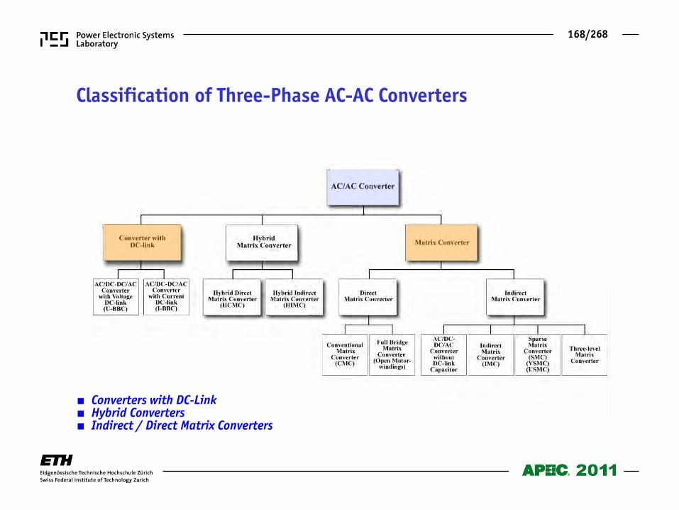
168/268
Classification of Three-Phase AC-AC Converters
Converters with DC-Link Hybrid Converters Indirect / Direct Matrix Converters
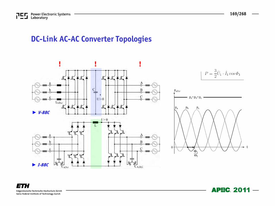
169/268
DC-Link AC-AC Converter Topologies
! ! !
V-BBC
I-BBC
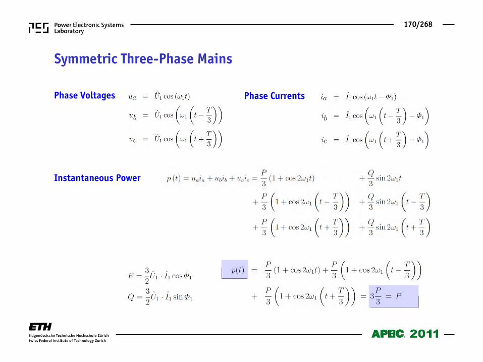
170/268
Symmetric Three-Phase Mains
Phase Voltages Phase Currents
Instantaneous Power
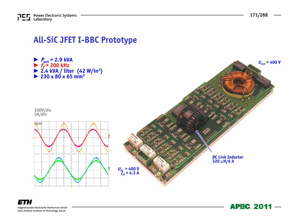
171/268
All-SiC JFET I-BBC Prototype
DC Link Inductor 320 H/6 A
Pout = 2.9 kVA fS = 200 kHz 2.4 kVA / liter (42 W/in3) 230 x 80 x 65 mm3
Uin = 400 V Iin = 4.3 A
Uout = 400 V
200V/div 5A/div
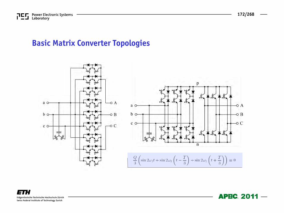
172/268
Basic Matrix Converter Topologies
173/268
V-BBC Voltage Space Vectors
Modulation DC-Link Current
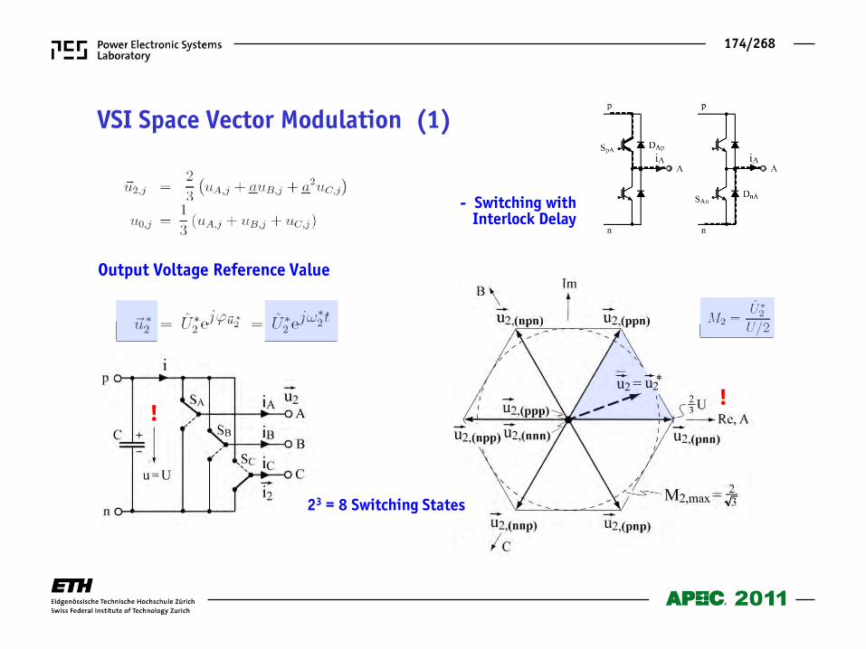
174/268
!
VSI Space Vector Modulation (1)
!
Output Voltage Reference Value
23 = 8 Switching States
- Switching with Interlock Delay
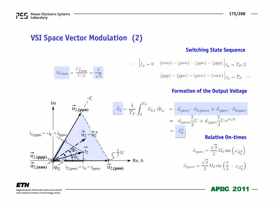
175/268
VSI Space Vector Modulation (2) Switching State Sequence
Relative On-times
Formation of the Output Voltage
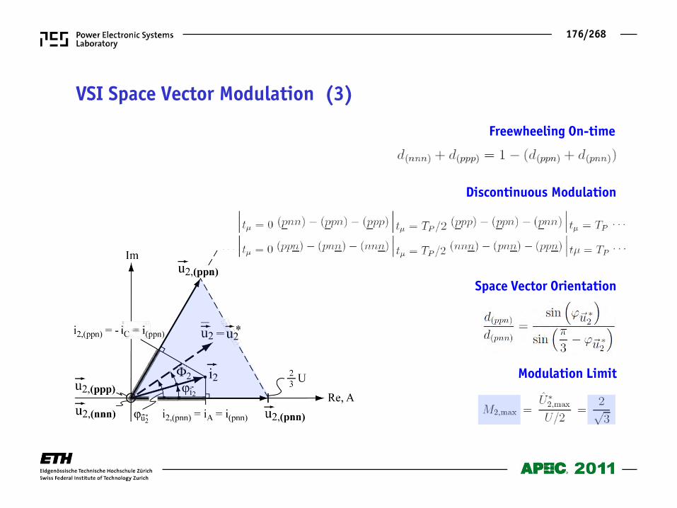
176/268
VSI Space Vector Modulation (3)
Discontinuous Modulation
Freewheeling On-time
Space Vector Orientation
Modulation Limit
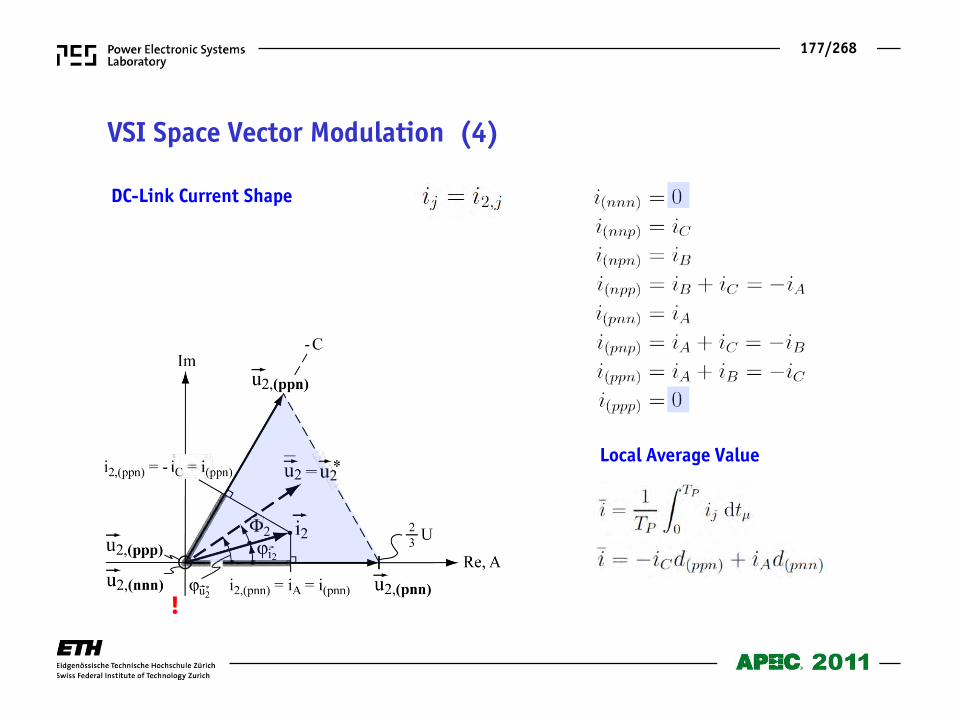
177/268
DC-Link Current Shape
!
Local Average Value
VSI Space Vector Modulation (4)
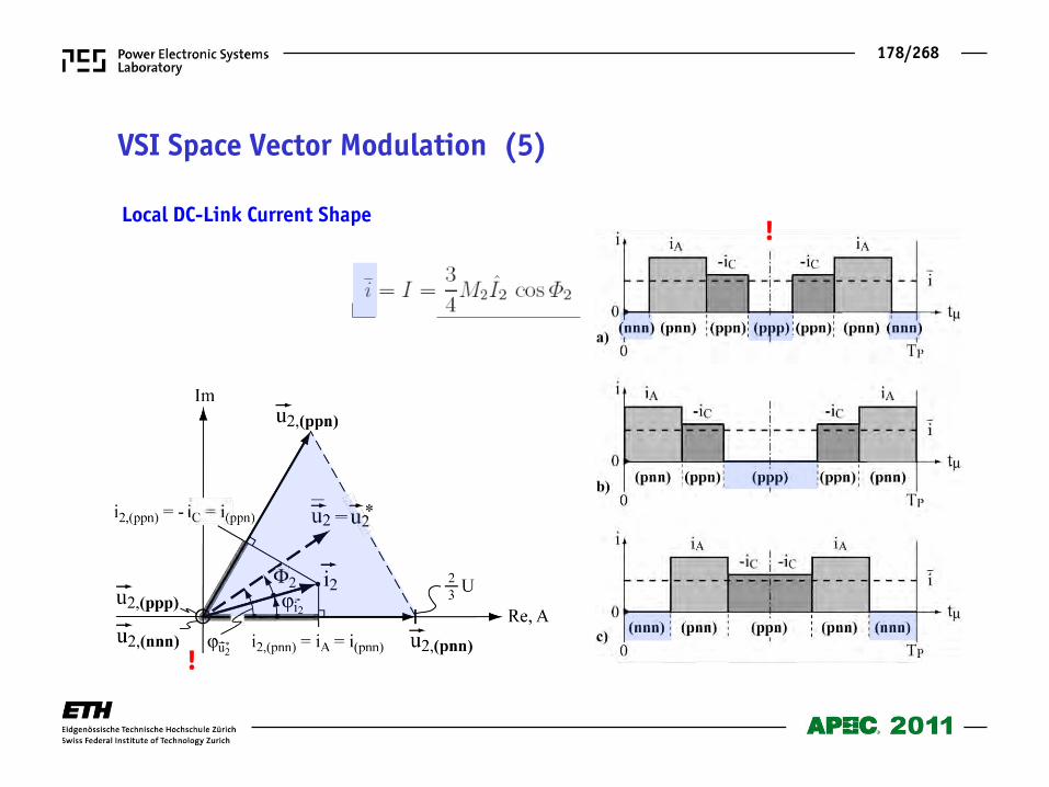
178/268
! Local DC-Link Current Shape
!
VSI Space Vector Modulation (5)
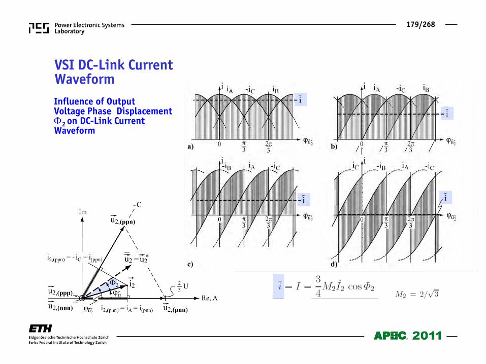
179/268
VSI DC-Link Current Waveform Influence of Output Voltage Phase Displacement 2 on DC-Link Current Waveform
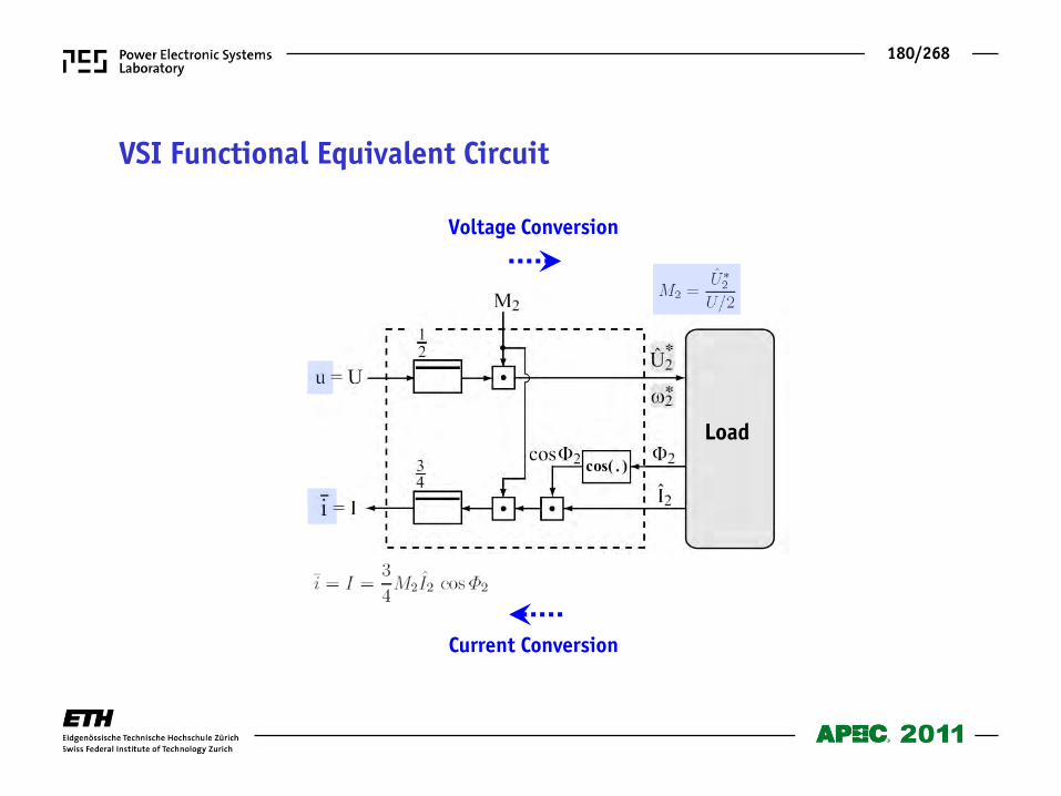
180/268
VSI Functional Equivalent Circuit
Voltage Conversion
Current Conversion
Load
181/268
I-BBC Current Space Vectors
Modulation DC Link Voltage
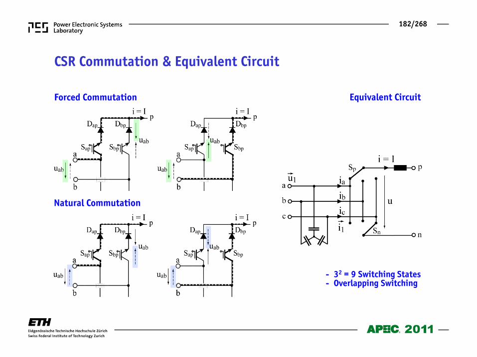
182/268
CSR Commutation & Equivalent Circuit
Forced Commutation
Natural Commutation
Equivalent Circuit
- 32 = 9 Switching States - Overlapping Switching
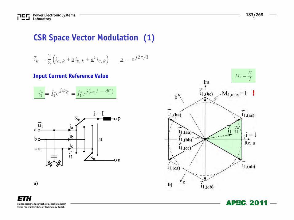
183/268
CSR Space Vector Modulation (1)
Input Current Reference Value
!
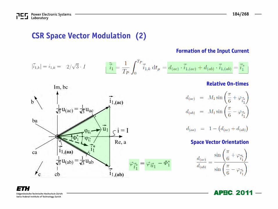
184/268
Formation of the Input Current
Relative On-times
Space Vector Orientation
CSR Space Vector Modulation (2)
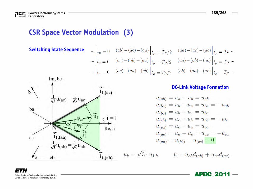
185/268
CSR Space Vector Modulation (3)
Switching State Sequence
DC-Link Voltage Formation
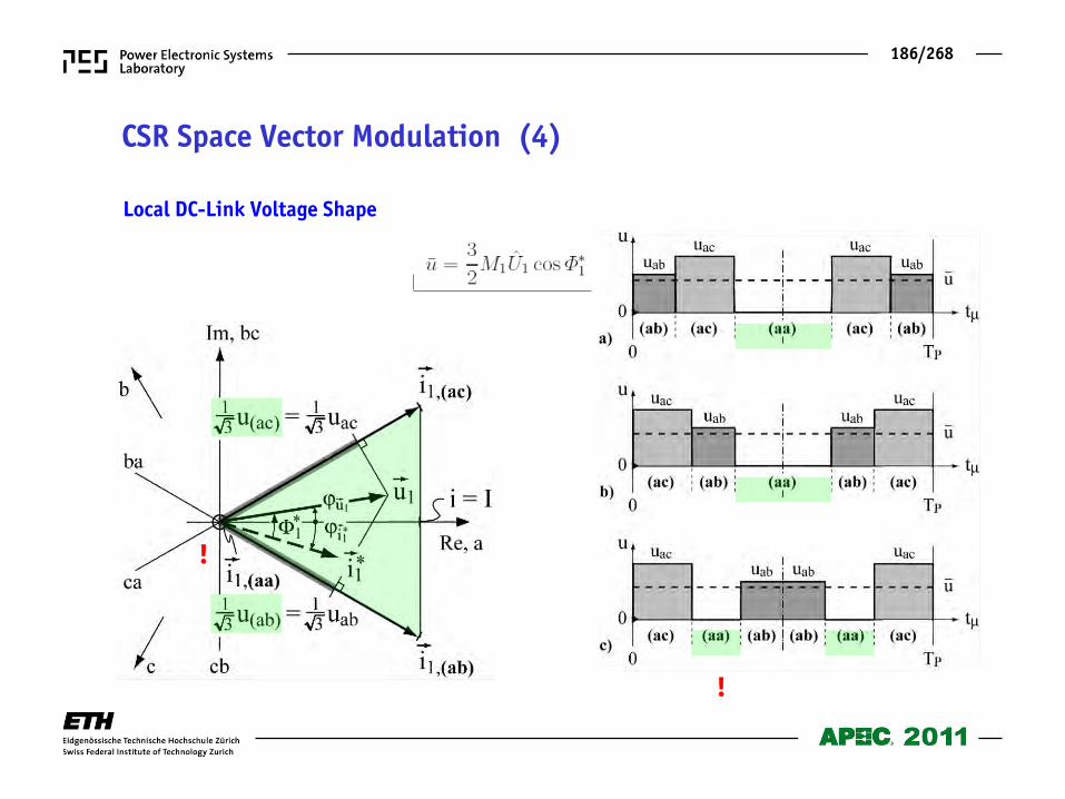
186/268
!
!
CSR Space Vector Modulation (4)
Local DC-Link Voltage Shape
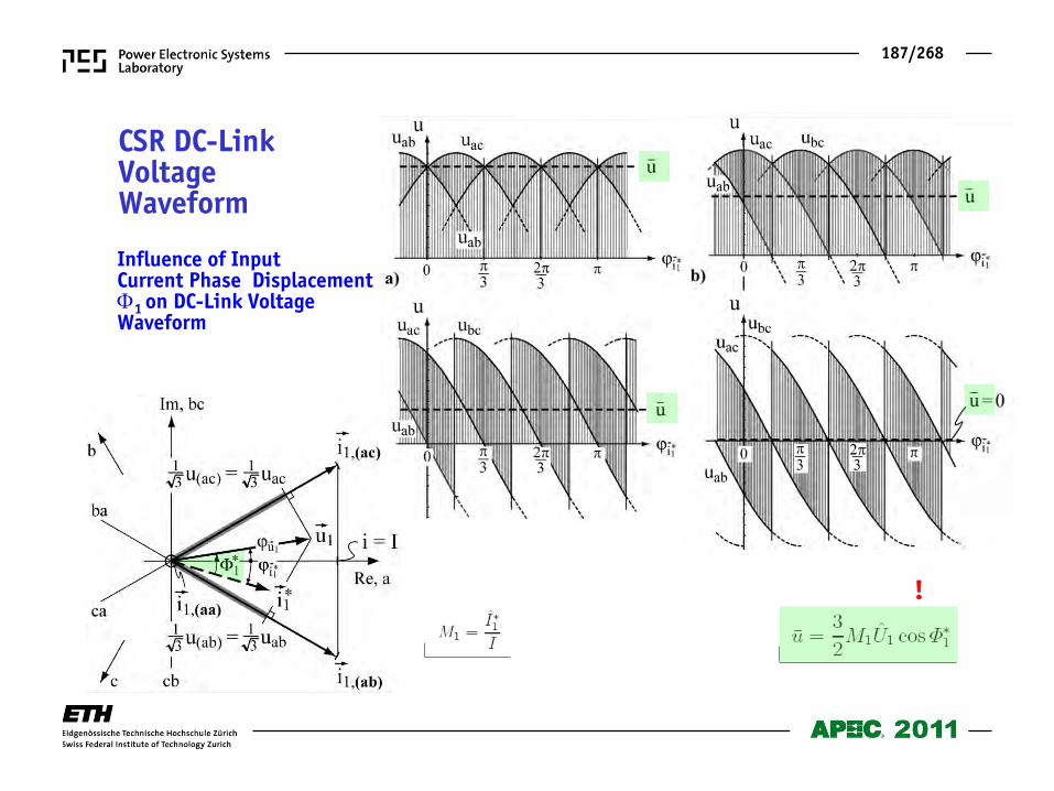
187/268
CSR DC-Link Voltage Waveform
!
Influence of Input Current Phase Displacement 1 on DC-Link Voltage Waveform
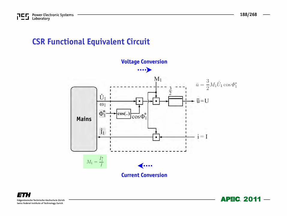
188/268
Voltage Conversion
Current Conversion
Mains
CSR Functional Equivalent Circuit
189/268
Fundamental Frequency Front End F
3E
Derivation of MC Topologies
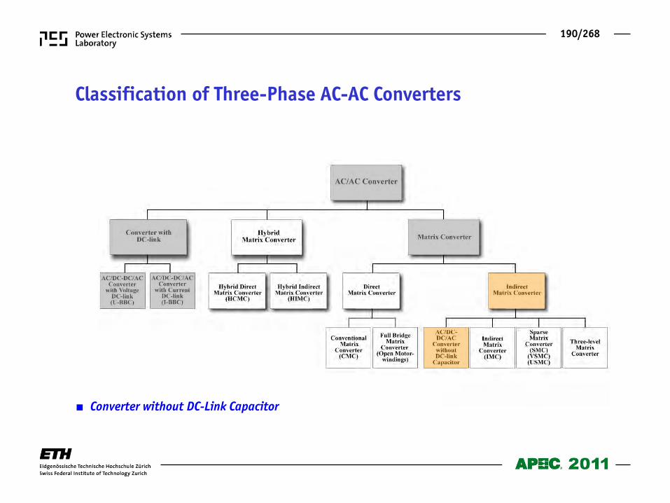
190/268
Classification of Three-Phase AC-AC Converters
Converter without DC-Link Capacitor
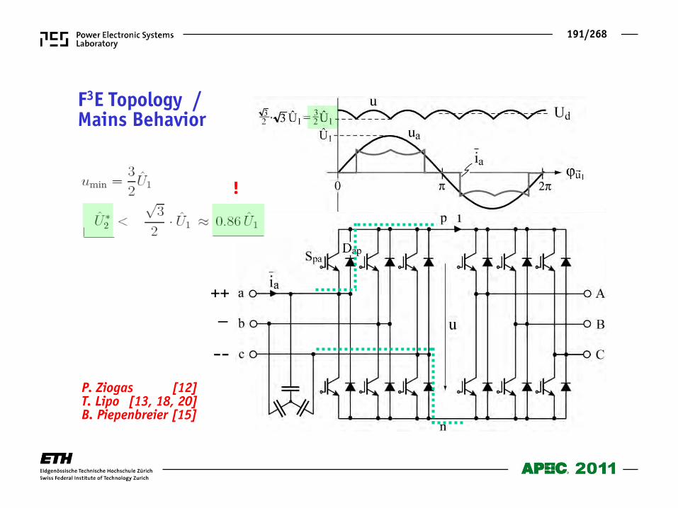
191/268
++
- -
F3E Topology / Mains Behavior
!
P. Ziogas [12] T. Lipo [13, 18, 20] B. Piepenbreier [15]
192/268
Indirect Matrix Converter – IMC Space Vectors Modulation Simulation
Experimental Results

193/268
Classification of Three-Phase AC-AC Converters
Indirect Matrix Converter
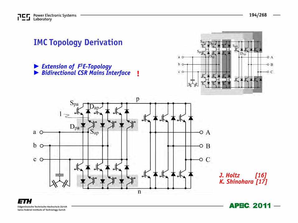
194/268
IMC Topology Derivation
Extension of F3E-Topology Bidirectional CSR Mains Interface !
J. Holtz [16] K. Shinohara [17]
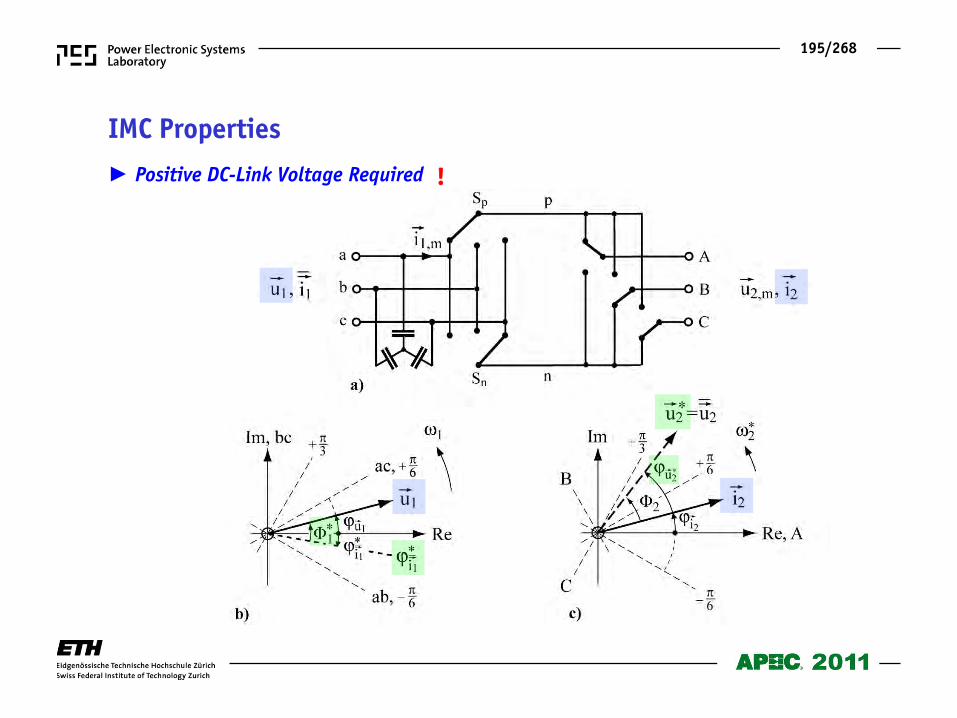
195/268
IMC Properties Positive DC-Link Voltage Required !
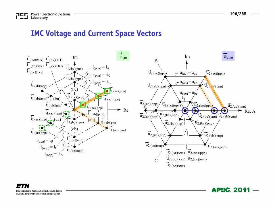
196/268
IMC Voltage and Current Space Vectors

197/268
IMC Space Vector Modulation (1)
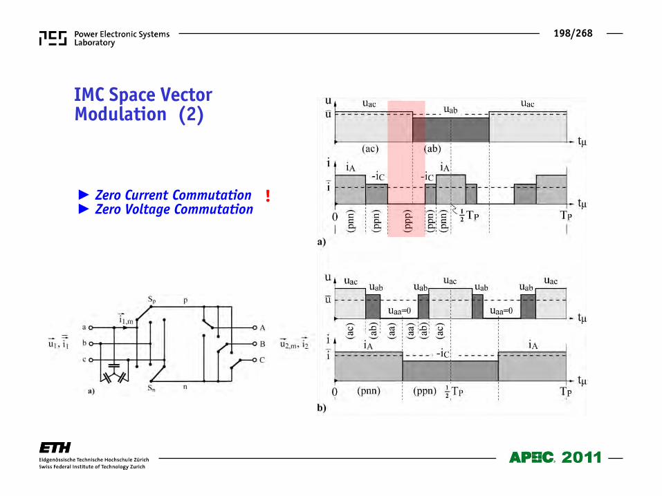
198/268
IMC Space Vector Modulation (2)
Zero Current Commutation Zero Voltage Commutation
!
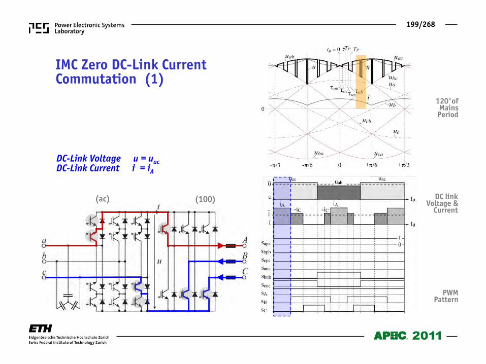
199/268
DC-Link Voltage u = uac DC-Link Current i = iA
(100) (ac)
IMC Zero DC-Link Current Commutation (1)
PWM Pattern
120°of Mains Period
DC link Voltage &
Current
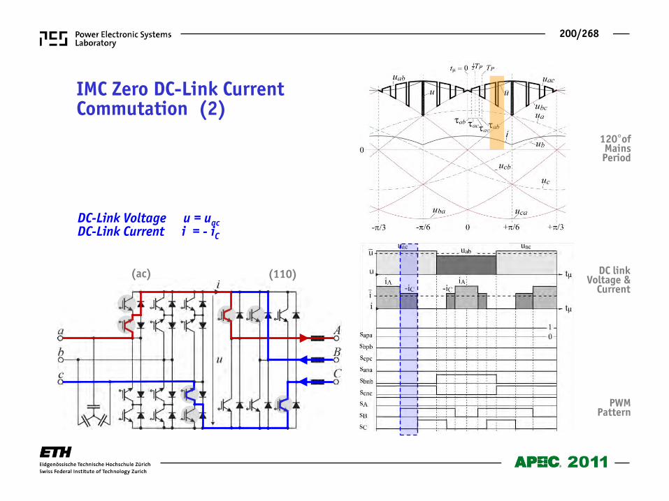
200/268
120°of Mains Period
DC link Voltage &
Current
IMC Zero DC-Link Current Commutation (2)
DC-Link Voltage u = uac DC-Link Current i = - iC
(110) (ac)
PWM Pattern
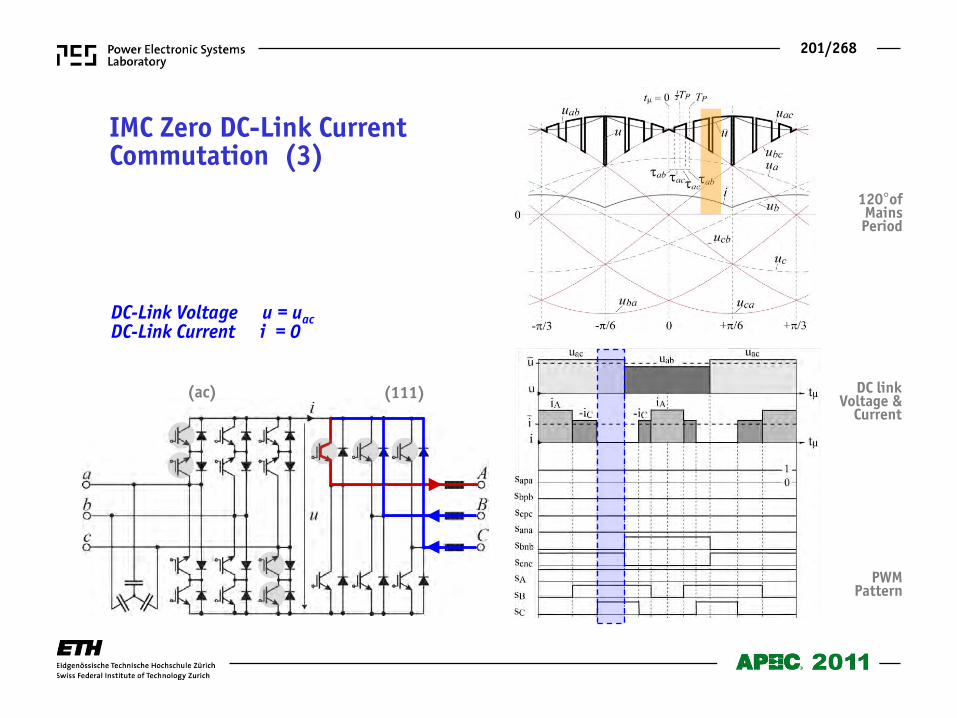
201/268
120°of Mains Period
DC link Voltage &
Current
IMC Zero DC-Link Current Commutation (3)
DC-Link Voltage u = uac DC-Link Current i = 0
(111) (ac)
PWM Pattern
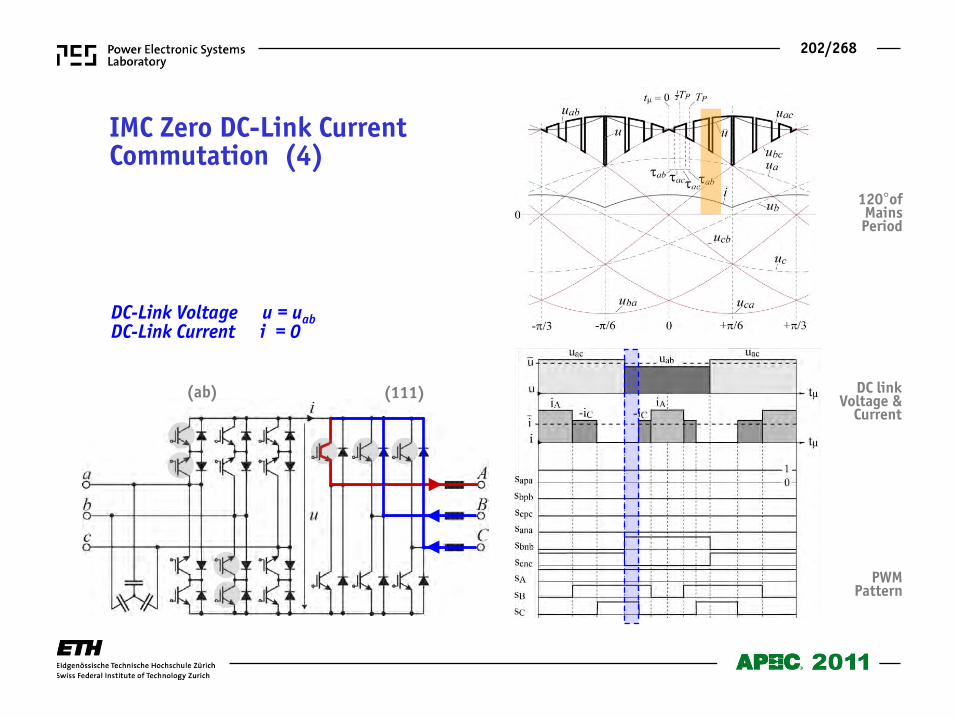
202/268
120°of Mains Period
DC link Voltage &
Current
IMC Zero DC-Link Current Commutation (4)
DC-Link Voltage u = uab DC-Link Current i = 0
(111) (ab)
PWM Pattern
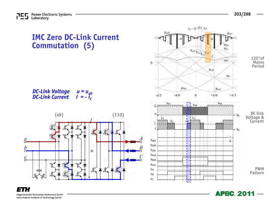
203/268
120°of Mains Period
DC link Voltage &
Current
DC-Link Voltage u = uab DC-Link Current i = - iC
(110) (ab)
IMC Zero DC-Link Current Commutation (5)
PWM Pattern

204/268
DC-Link Voltage u = uab DC-Link Current i = iA
IMC Zero DC-Link Current Commutation (6)
120°of Mains Period
DC link Voltage &
Current (100) (ab)
PWM Pattern
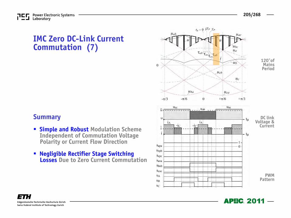
205/268
Summary Simple and Robust Modulation Scheme Independent of Commutation Voltage Polarity or Current Flow Direction Negligible Rectifier Stage Switching Losses Due to Zero Current Commutation
120°of Mains Period
DC link Voltage &
Current
PWM Pattern
IMC Zero DC-Link Current Commutation (7)
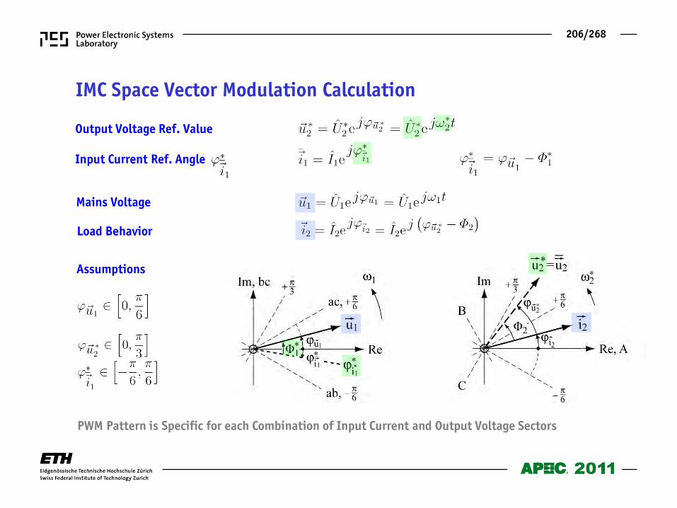
206/268
IMC Space Vector Modulation Calculation
Output Voltage Ref. Value
Input Current Ref. Angle
Mains Voltage
Assumptions
Load Behavior
PWM Pattern is Specific for each Combination of Input Current and Output Voltage Sectors
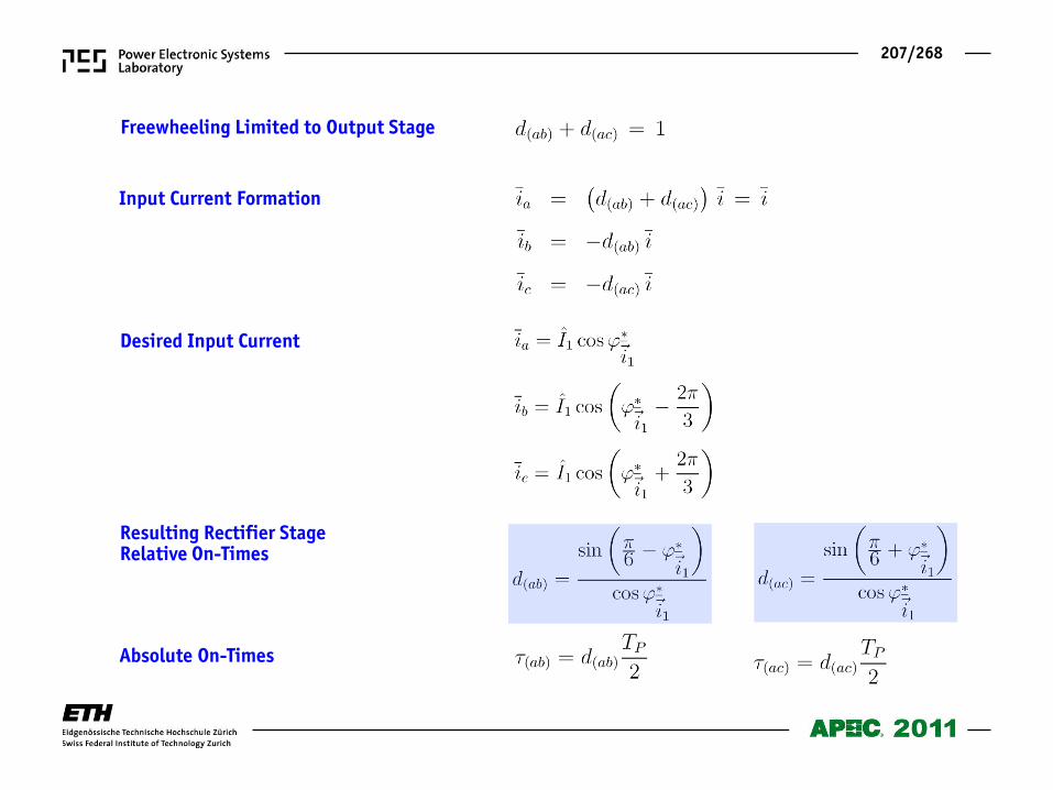
207/268
Freewheeling Limited to Output Stage
Input Current Formation
Desired Input Current
Resulting Rectifier Stage Relative On-Times
Absolute On-Times
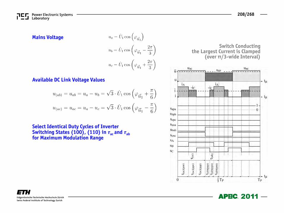
208/268
Mains Voltage
Available DC Link Voltage Values
Select Identical Duty Cycles of Inverter Switching States (100), (110) in τac and τab for Maximum Modulation Range
Switch Conducting the Largest Current is Clamped
(over π/3-wide Interval)
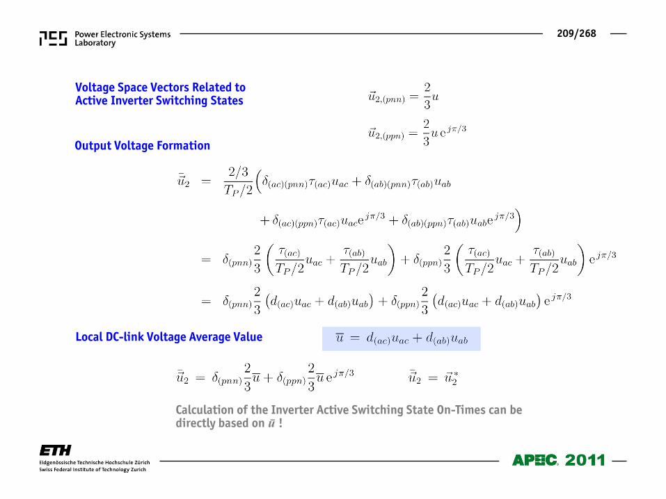
209/268
Voltage Space Vectors Related to Active Inverter Switching States
Output Voltage Formation
Local DC-link Voltage Average Value
Calculation of the Inverter Active Switching State On-Times can be directly based on ū !
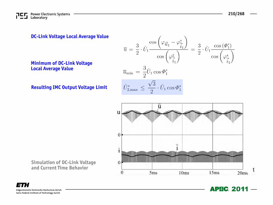
210/268
DC-Link Voltage Local Average Value
Simulation of DC-Link Voltage and Current Time Behavior
Minimum of DC-Link Voltage Local Average Value
Resulting IMC Output Voltage Limit
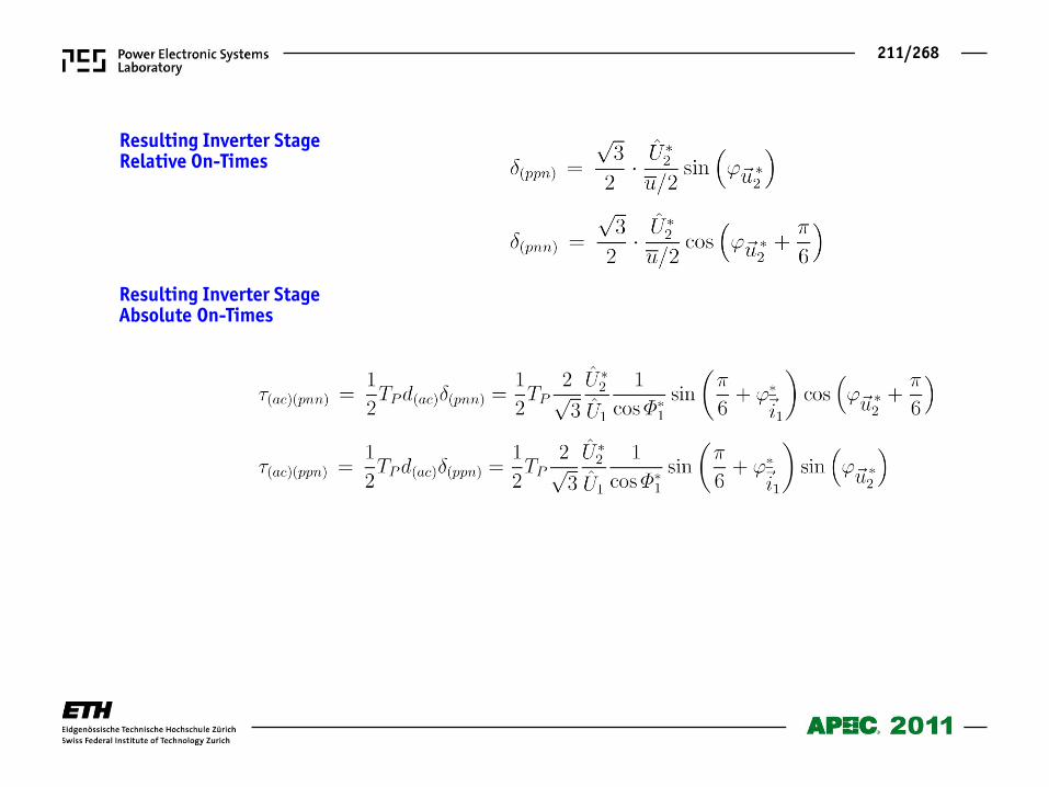
211/268
Resulting Inverter Stage Relative On-Times
Resulting Inverter Stage Absolute On-Times
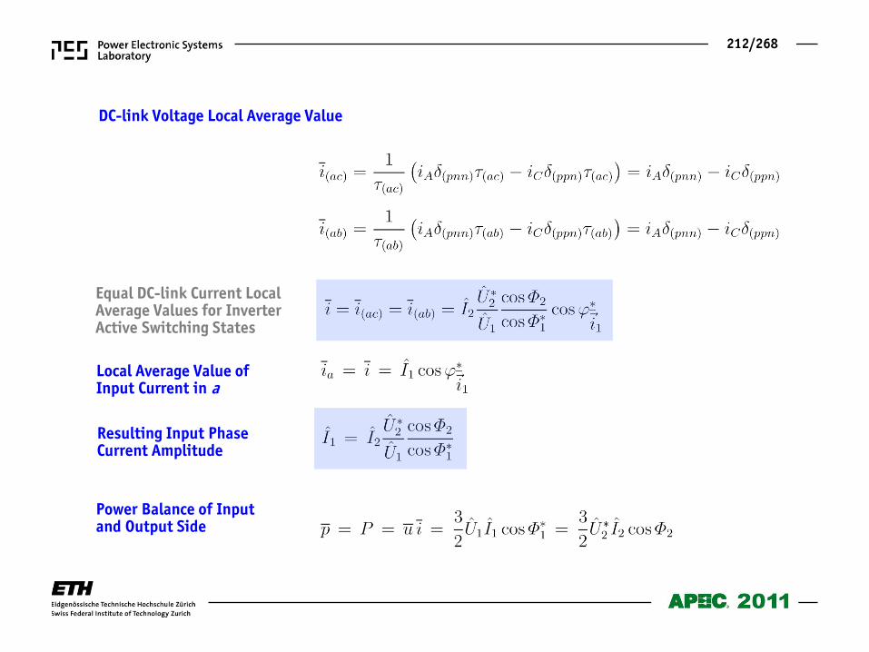
212/268
DC-link Voltage Local Average Value
Equal DC-link Current Local Average Values for Inverter Active Switching States
Local Average Value of Input Current in a
Resulting Input Phase Current Amplitude
Power Balance of Input and Output Side
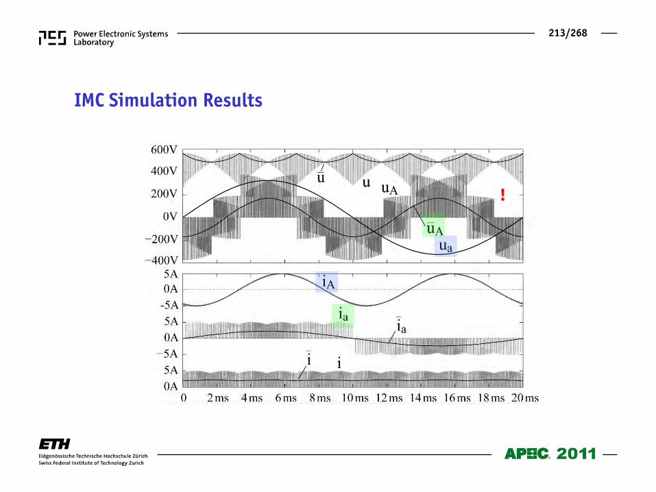
213/268
IMC Simulation Results
!
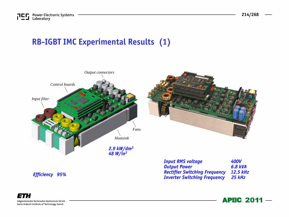
214/268
Input filter
Heatsink
Fans
Output connectors
Control boards
2.9 kW/dm3=~
Input RMS voltage 400V Output Power 6.8 kVA Rectifier Switching Frequency 12.5 kHz Inverter Switching Frequency 25 kHz
2.9 kW/dm3
48 W/in3
Efficiency 95%
RB-IGBT IMC Experimental Results (1)
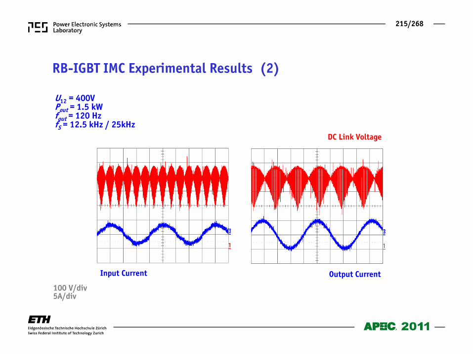
215/268
U12 = 400V Pout = 1.5 kW fout = 120 Hz fS = 12.5 kHz / 25kHz
Output Current
DC Link Voltage
Input Current
100 V/div 5A/div
RB-IGBT IMC Experimental Results (2)
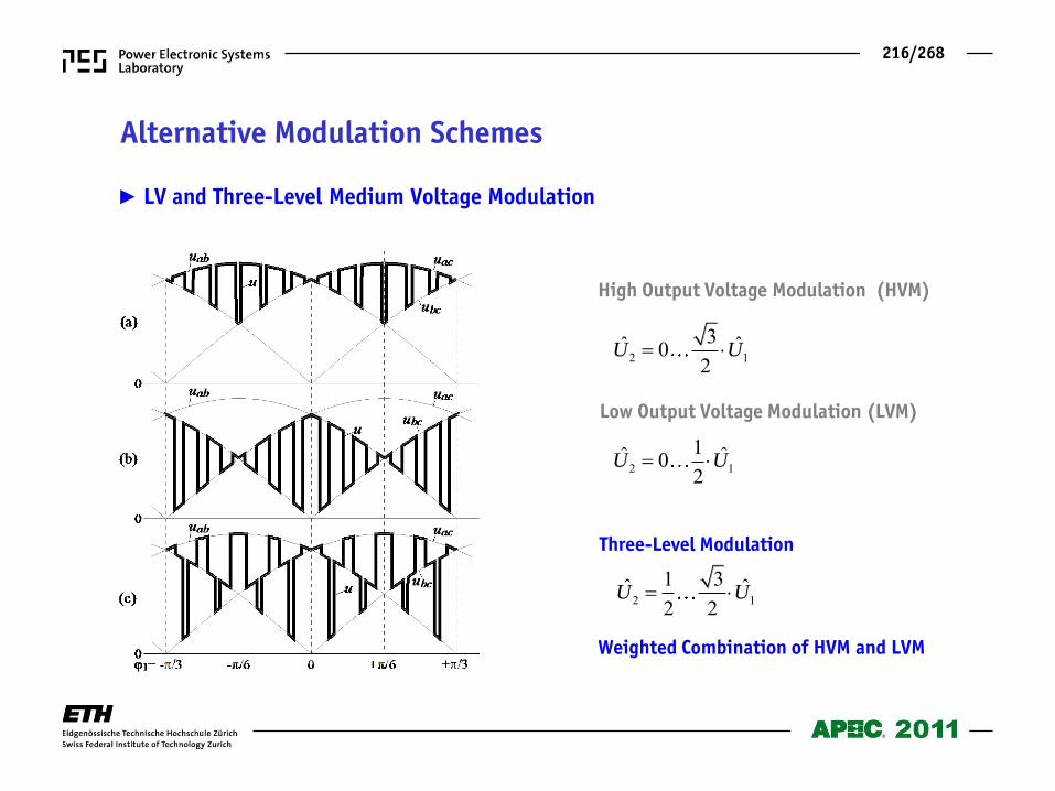
216/268
High Output Voltage Modulation (HVM)
Low Output Voltage Modulation (LVM)
Three-Level Modulation
2 13ˆ ˆ0
2U U
2 11ˆ ˆ02
U U
2 11 3ˆ ˆ2 2
U U
LV and Three-Level Medium Voltage Modulation
Weighted Combination of HVM and LVM
Alternative Modulation Schemes
217/268
Conventional Matrix Converter - CMC Modulation
Multi-Step Commutation
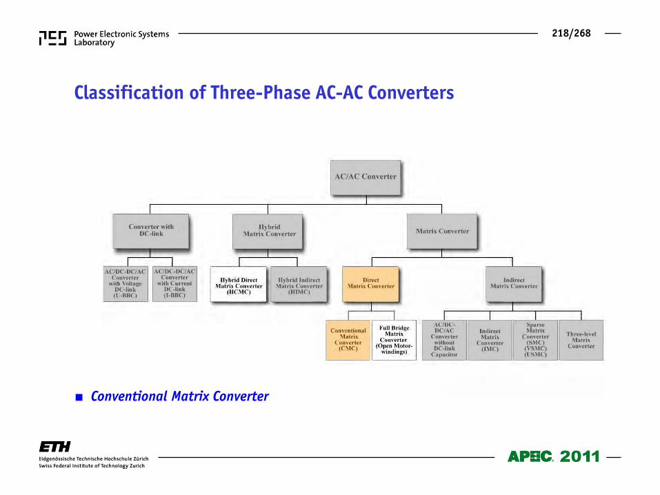
218/268
Classification of Three-Phase AC-AC Converters
Conventional Matrix Converter
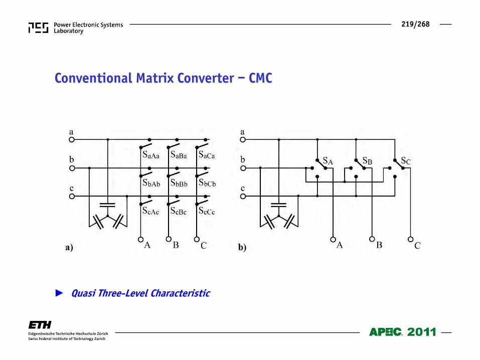
219/268
Conventional Matrix Converter – CMC
Quasi Three-Level Characteristic
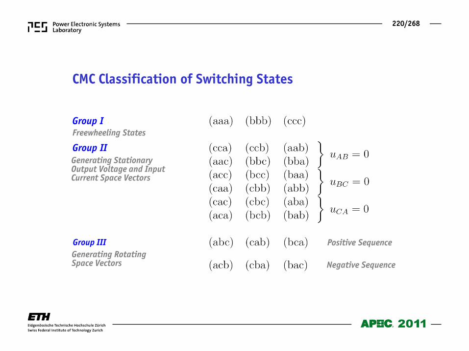
220/268
CMC Classification of Switching States
Freewheeling States
Group II
Group III
Generating Stationary Output Voltage and Input Current Space Vectors
Generating Rotating Space Vectors
Positive Sequence
Negative Sequence
Group I
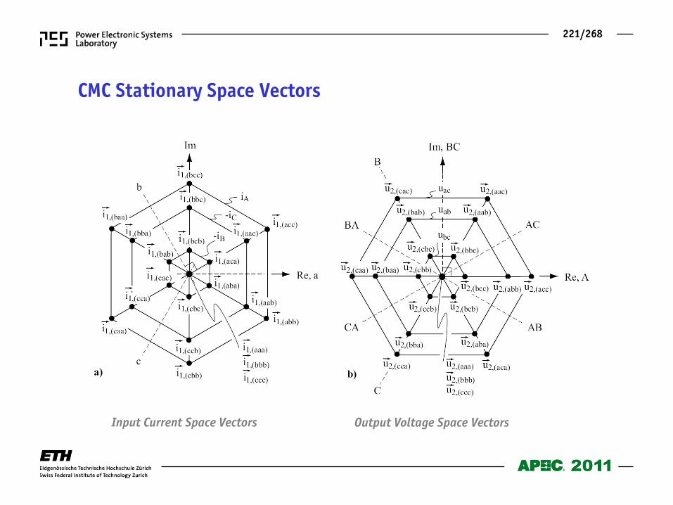
221/268
CMC Stationary Space Vectors
Output Voltage Space Vectors Input Current Space Vectors
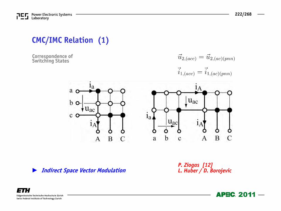
222/268
Indirect Space Vector Modulation P. Ziogas [12] L. Huber / D. Borojevic
Correspondence of Switching States
CMC/IMC Relation (1)

223/268
Correspondence of Switching States
IMC
CMC
IMC
CMC
CMC/IMC Relation (2)
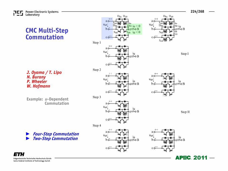
224/268
CMC Multi-Step Commutation
J. Oyama / T. Lipo N. Burany P. Wheeler W. Hofmann
Four-Step Commutation Two-Step Commutation
Example: u- Dependent Commutation
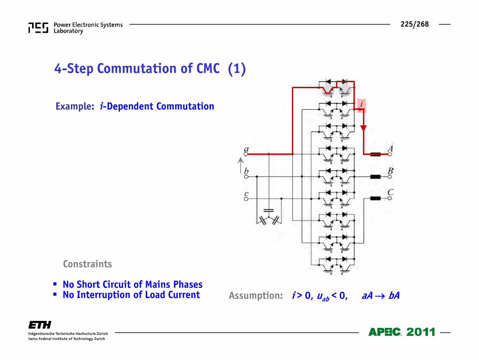
225/268
4-Step Commutation of CMC (1)
Constraints No Short Circuit of Mains Phases No Interruption of Load Current
Example: i-Dependent Commutation
Assumption: i > 0, uab < 0, aA bA
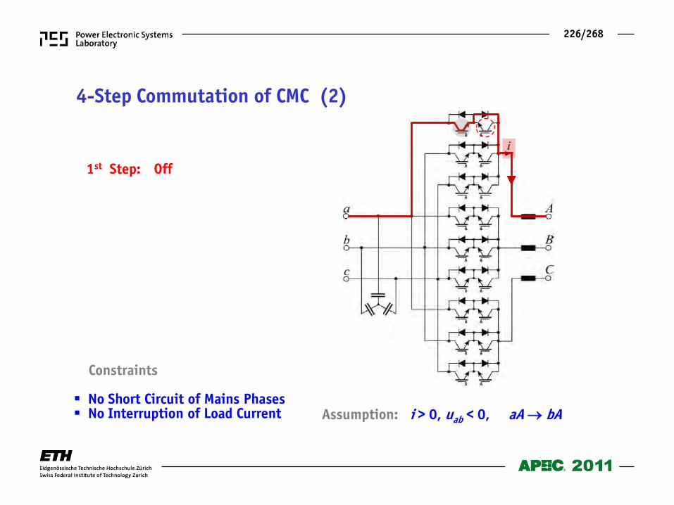
226/268
Constraints No Short Circuit of Mains Phases No Interruption of Load Current
4-Step Commutation of CMC (2)
1st Step: Off
Assumption: i > 0, uab < 0, aA bA
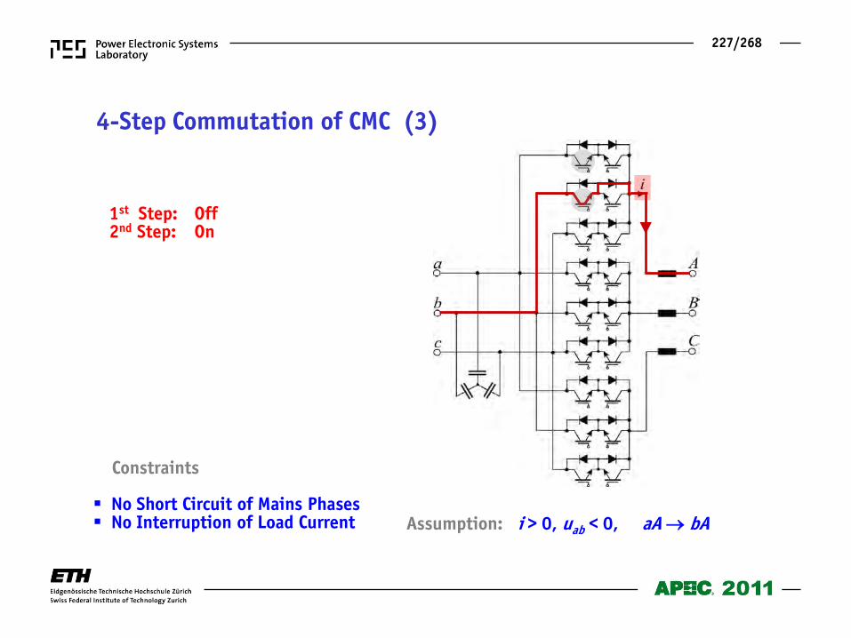
227/268
1st Step: Off 2nd Step: On
Constraints No Short Circuit of Mains Phases No Interruption of Load Current
4-Step Commutation of CMC (3)
Assumption: i > 0, uab < 0, aA bA
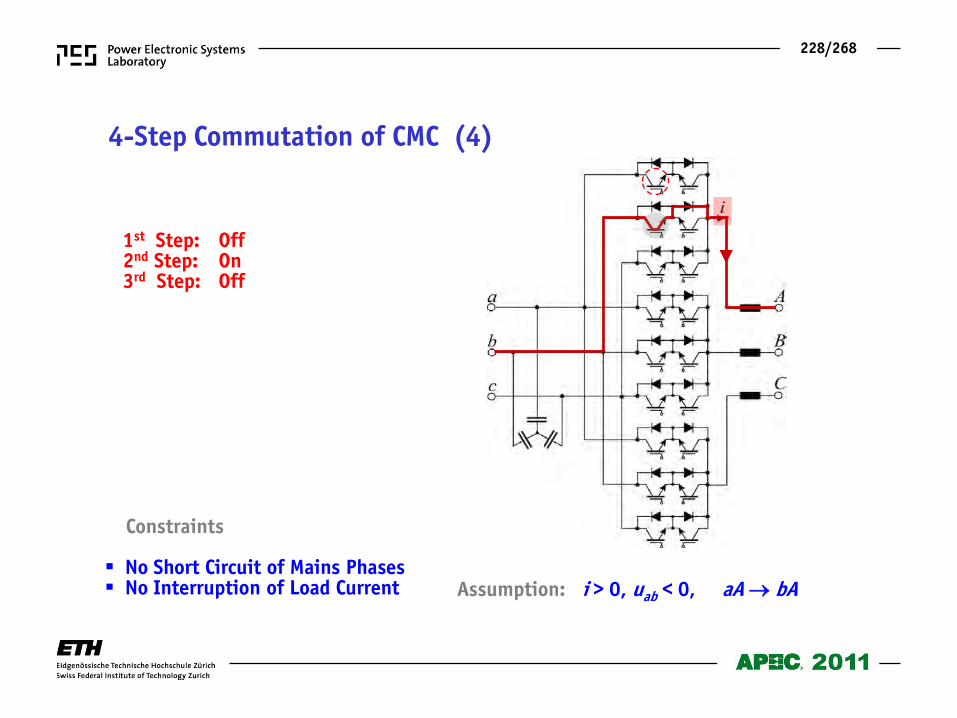
228/268
1st Step: Off 2nd Step: On 3rd Step: Off
Constraints No Short Circuit of Mains Phases No Interruption of Load Current
4-Step Commutation of CMC (4)
Assumption: i > 0, uab < 0, aA bA
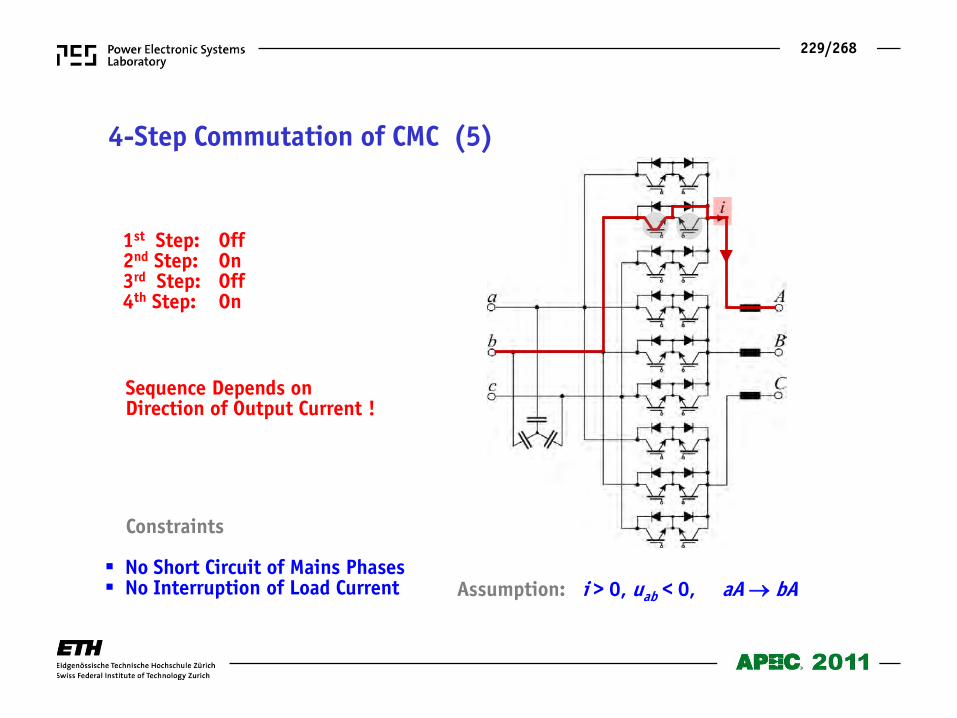
229/268
Sequence Depends on Direction of Output Current !
1st Step: Off 2nd Step: On 3rd Step: Off 4th Step: On
Constraints No Short Circuit of Mains Phases No Interruption of Load Current
4-Step Commutation of CMC (5)
Assumption: i > 0, uab < 0, aA bA
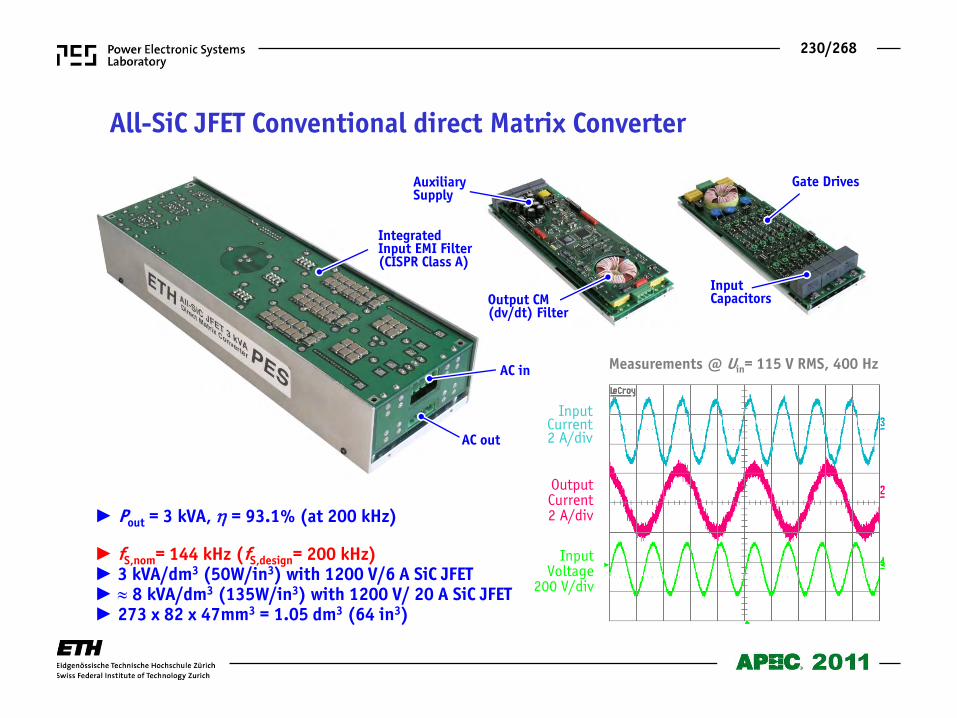
230/268
All-SiC JFET Conventional direct Matrix Converter
Pout = 3 kVA, = 93.1% (at 200 kHz) fS,nom= 144 kHz (fS,design= 200 kHz) 3 kVA/dm3 (50W/in3) with 1200 V/6 A SiC JFET 8 kVA/dm3 (135W/in3) with 1200 V/ 20 A SiC JFET 273 x 82 x 47mm3 = 1.05 dm3 (64 in3)
Measurements @ Uin= 115 V RMS, 400 Hz
AC out
AC in
Output CM (dv/dt) Filter
Auxiliary Supply
Integrated Input EMI Filter (CISPR Class A)
Gate Drives
Input Capacitors
Input Voltage
200 V/div
Input Current 2 A/div
Output Current 2 A/div
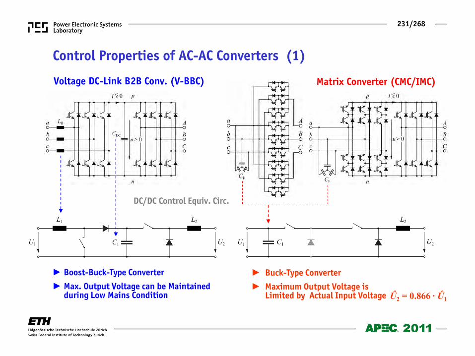
231/268
Control Properties of AC-AC Converters (1)
Voltage DC-Link B2B Conv. (V-BBC) Matrix Converter (CMC/IMC)
DC/DC Control Equiv. Circ.
Boost-Buck-Type Converter
Max. Output Voltage can be Maintained during Low Mains Condition
Buck-Type Converter
Maximum Output Voltage is Limited by Actual Input Voltage Û2 = 0.866 ∙ Û1
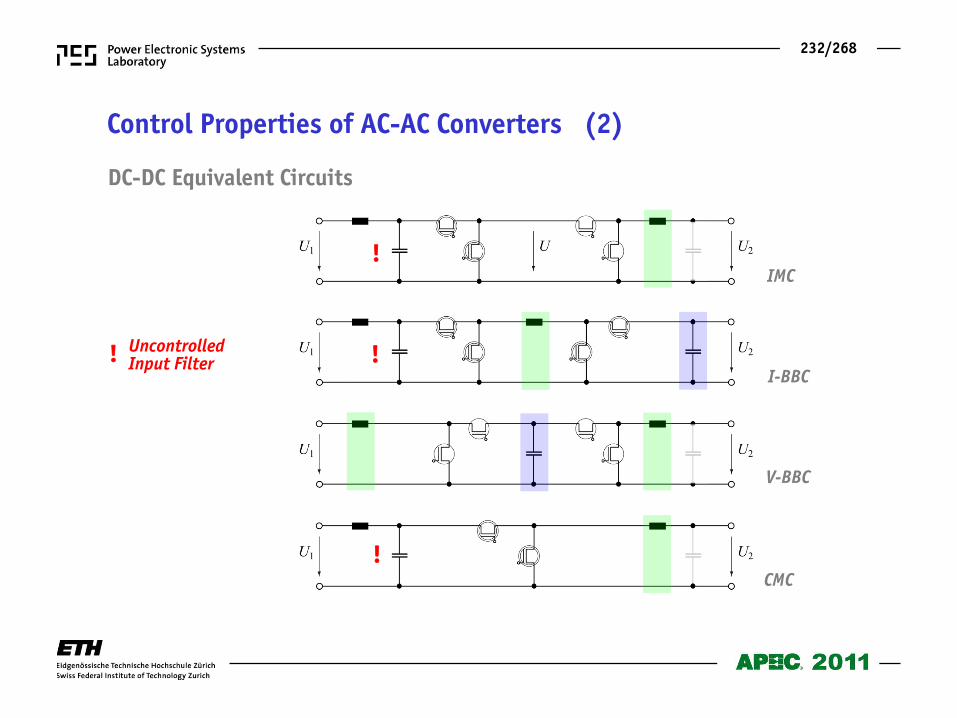
232/268
Control Properties of AC-AC Converters (2)
DC-DC Equivalent Circuits
!
!
!
! Uncontrolled Input Filter
IMC
I-BBC
V-BBC
CMC
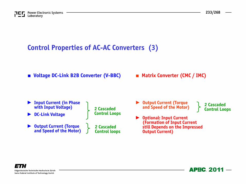
233/268
Voltage DC-Link B2B Converter (V-BBC) Matrix Converter (CMC / IMC)
Input Current (in Phase with Input Voltage)
DC-Link Voltage
Output Current (Torque and Speed of the Motor)
Output Current (Torque and Speed of the Motor) 2 Cascaded
Control Loops
2 Cascaded Control loops
2 Cascaded Control Loops
Optional: Input Current (Formation of Input Current still Depends on the Impressed Output Current)
Control Properties of AC-AC Converters (3)
234/268
Comparative Evaluation DC Link Converters Matrix Converters
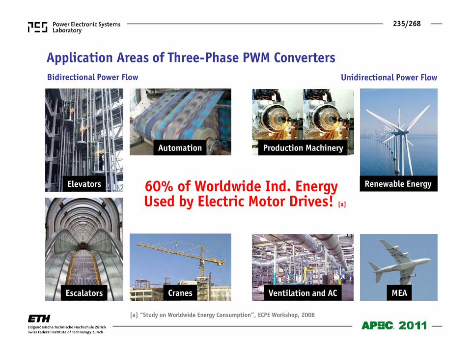
235/268
Bidirectional Power Flow Unidirectional Power Flow
Elevators
Escalators Cranes
Roller Test Benches
Automation Production Machinery
Pumps and Compressors
Ventilation and AC
Renewable Energy
MEA
60% of Worldwide Ind. Energy
Used by Electric Motor Drives! [a]
Application Areas of Three-Phase PWM Converters
[a] “Study on Worldwide Energy Consumption”, ECPE Workshop, 2008
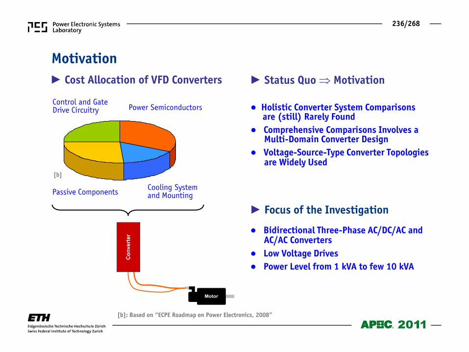
236/268
[b]: Based on “ECPE Roadmap on Power Electronics, 2008”
Motor
Conv
erte
r
Power Semiconductors
Cooling System and Mounting
Control and Gate Drive Circuitry
Passive Components
Holistic Converter System Comparisons are (still) Rarely Found
Comprehensive Comparisons Involves a Multi-Domain Converter Design
Voltage-Source-Type Converter Topologies are Widely Used
Cost Allocation of VFD Converters Status Quo Motivation
Bidirectional Three-Phase AC/DC/AC and AC/AC Converters
Low Voltage Drives
Power Level from 1 kVA to few 10 kVA
Focus of the Investigation
Motivation
[b]
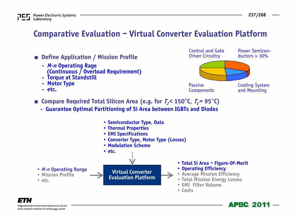
237/268
Define Application / Mission Profile
- M-n Operating Rage (Continuous / Overload Requirement) - Torque at Standstill - Motor Type - etc. Compare Required Total Silicon Area (e.g. for TJ < 150°C, TC = 95°C)
- Guarantee Optimal Partitioning of Si Area between IGBTs and Diodes
• M-n Operating Range • Mission Profile • etc.
• Semiconductor Type, Data • Thermal Properties • EMI Specifications • Converter Type, Motor Type (Losses) • Modulation Scheme • etc.
• Total Si Area – Figure-Of-Merit • Operating Efficiency • Average Mission Efficiency • Total Mission Energy Losses • EMI Filter Volume • Costs
Virtual Converter Evaluation Platform
Power Semicon- ductors 30%
Cooling System and Mounting
Control and Gate Driver Circuitry
Passive Components
Comparative Evaluation – Virtual Converter Evaluation Platform
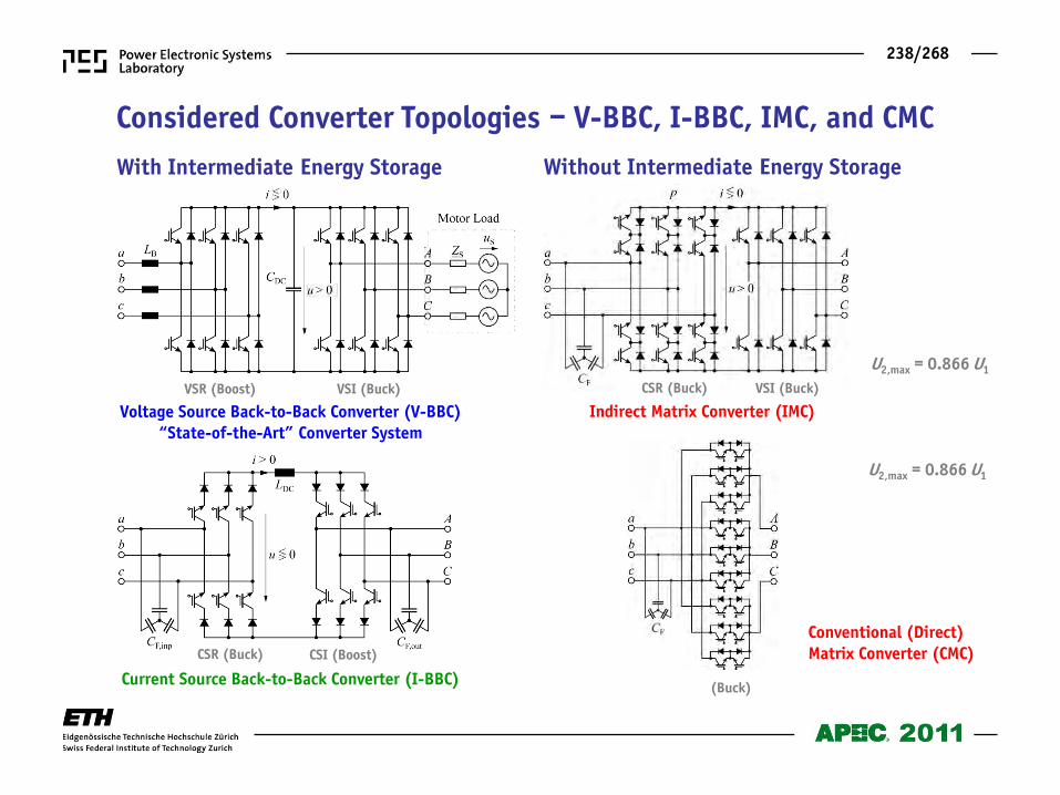
238/268
Current Source Back-to-Back Converter (I-BBC)
Conventional (Direct) Matrix Converter (CMC)
Voltage Source Back-to-Back Converter (V-BBC) “State-of-the-Art” Converter System
With Intermediate Energy Storage Without Intermediate Energy Storage
Indirect Matrix Converter (IMC) VSR (Boost) VSI (Buck) CSR (Buck) VSI (Buck)
CSR (Buck) CSI (Boost)
(Buck)
U2,max = 0.866 U1
U2,max = 0.866 U1
Considered Converter Topologies – V-BBC, I-BBC, IMC, and CMC
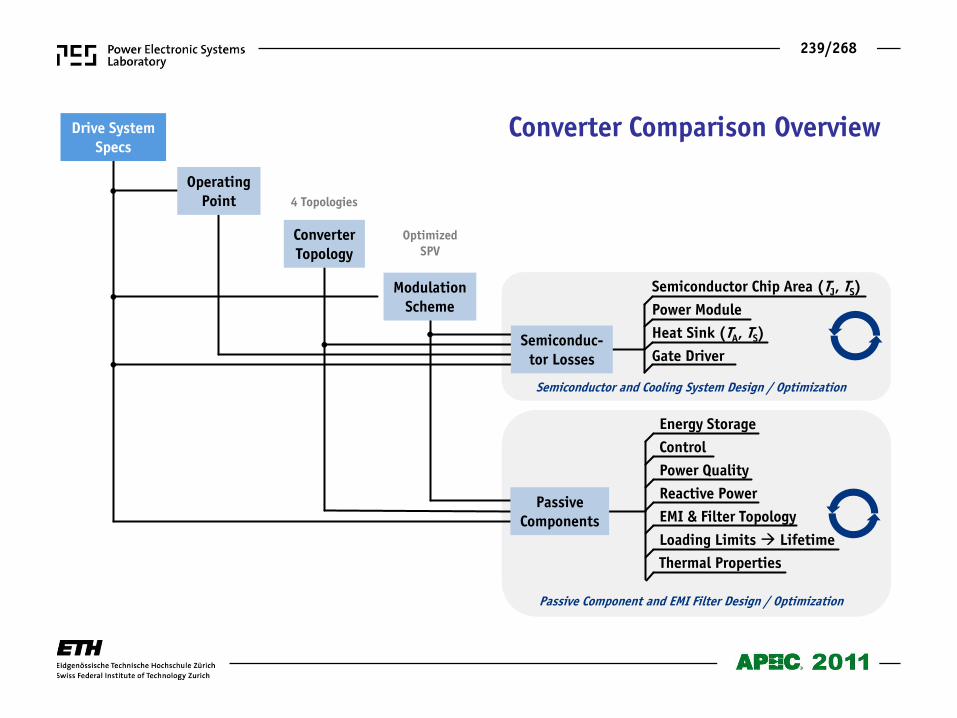
239/268
Converter Comparison Overview
Semiconductor Chip Area (TJ, TS) Power Module Heat Sink (TA, TS) Gate Driver
Semiconductor and Cooling System Design / Optimization
Energy Storage Control Power Quality Reactive Power EMI & Filter Topology Loading Limits Lifetime Thermal Properties
Converter Topology
Modulation Scheme
Operating Point
Drive System Specs
Semiconduc- tor Losses
Passive Component and EMI Filter Design / Optimization
Passive Components
4 Topologies
Optimized SPV
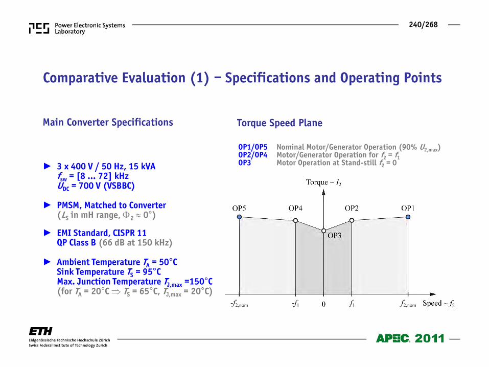
240/268
OP1/OP5 Nominal Motor/Generator Operation (90% U2,max) OP2/OP4 Motor/Generator Operation for f2 = f1 OP3 Motor Operation at Stand-still f2 = 0
Torque Speed Plane
3 x 400 V / 50 Hz, 15 kVA fsw = [8 … 72] kHz UDC = 700 V (VSBBC) PMSM, Matched to Converter (LS in mH range, 2 0°) EMI Standard, CISPR 11 QP Class B (66 dB at 150 kHz) Ambient Temperature TA = 50°C Sink Temperature TS = 95°C Max. Junction Temperature TJ,max =150°C (for TA = 20°C TS = 65°C, TJ,max = 20°C)
Main Converter Specifications
Comparative Evaluation (1) – Specifications and Operating Points
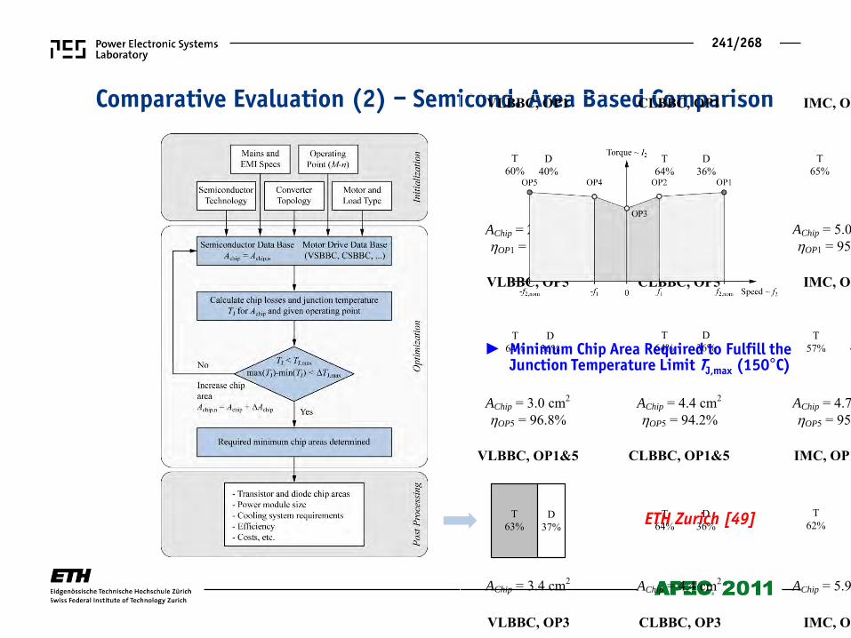
241/268
Comparative Evaluation (2) – Semicond. Area Based Comparison
AChip = 5.0 cm2
OP1 = 95.5%AChip = 4.4 cm2
OP1 = 94.2%AChip = 2.9 cm2
OP1 = 96.7%
VLBBC, OP3
AChip = 7.9 cm2AChip = 6.1 cm2AChip = 5.0 cm2
AChip = 4.7 cm2
OP5 = 95.6%AChip = 4.4 cm2
OP5 = 94.2%AChip = 3.0 cm2
OP5 = 96.8%
CLBBC, OP3 IMC, OP3
VLBBC, OP1 CLBBC, OP1 IMC, OP1
VLBBC, OP5 CLBBC, OP5 IMC, OP5
T64%
D36%
T65%
D35%
T60%
D40%
T55%
D45%
T62%
D38%
T56%
D44%
T57%
D43%
T64%
D36%
T64%
D36%
AChip = 4.4 cm2
CLBBC, OP1&5
T64%
D36%
T62%
D38%
IMC, OP1&5
AChip = 5.9 cm2
T63%
D37%
VLBBC, OP1&5
AChip = 3.4 cm2
Minimum Chip Area Required to Fulfill the Junction Temperature Limit TJ,max (150°C)
ETH Zurich [49]
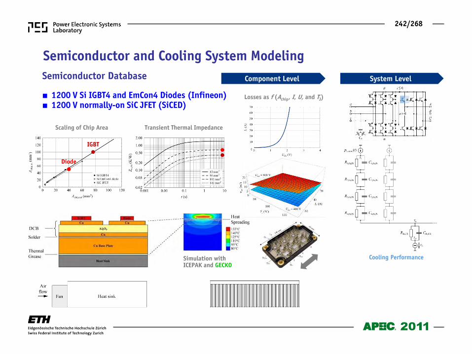
242/268
Simulation with ICEPAK and GECKO
Semiconductor Database
1200 V Si IGBT4 and EmCon4 Diodes (Infineon) 1200 V normally-on SiC JFET (SiCED)
Semiconductor and Cooling System Modeling
Cooling Performance
System Level Component Level
Losses as f (Achip, I, U, and TJ)
Transient Thermal Impedance
Diode
IGBT
Scaling of Chip Area
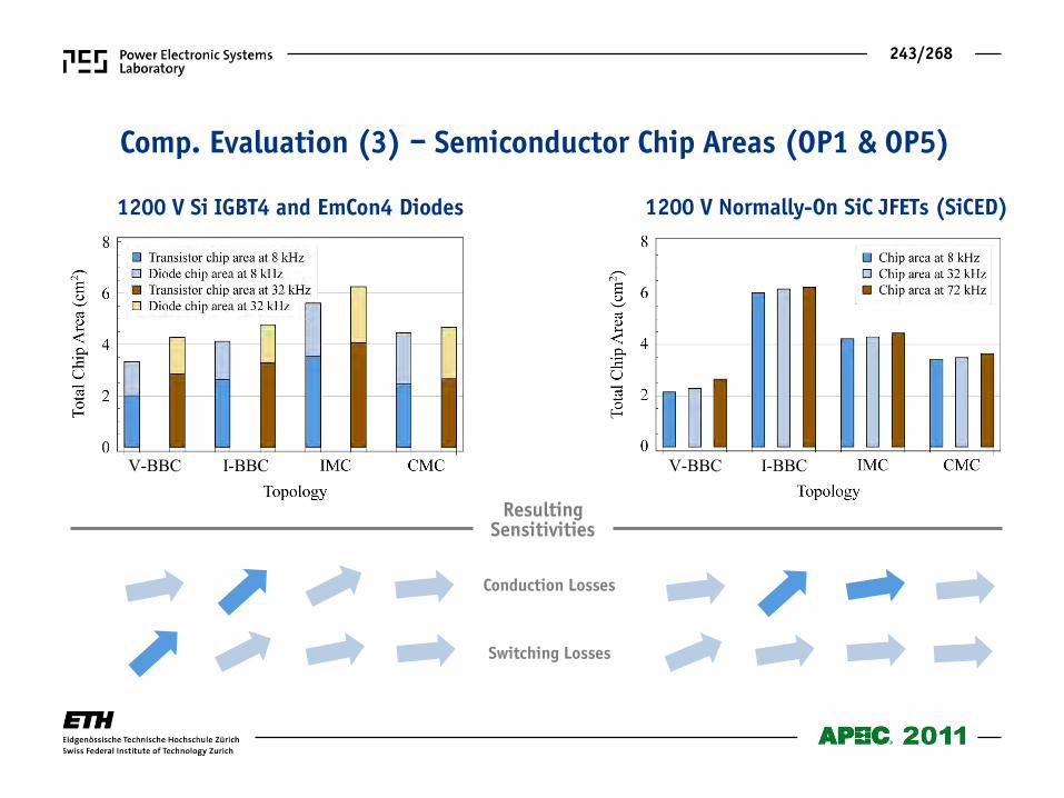
243/268
Comp. Evaluation (3) – Semiconductor Chip Areas (OP1 & OP5)
Conduction Losses
Switching Losses
Resulting Sensitivities
1200 V Si IGBT4 and EmCon4 Diodes 1200 V Normally-On SiC JFETs (SiCED)
I-BBC V-BBC I-BBC V-BBC
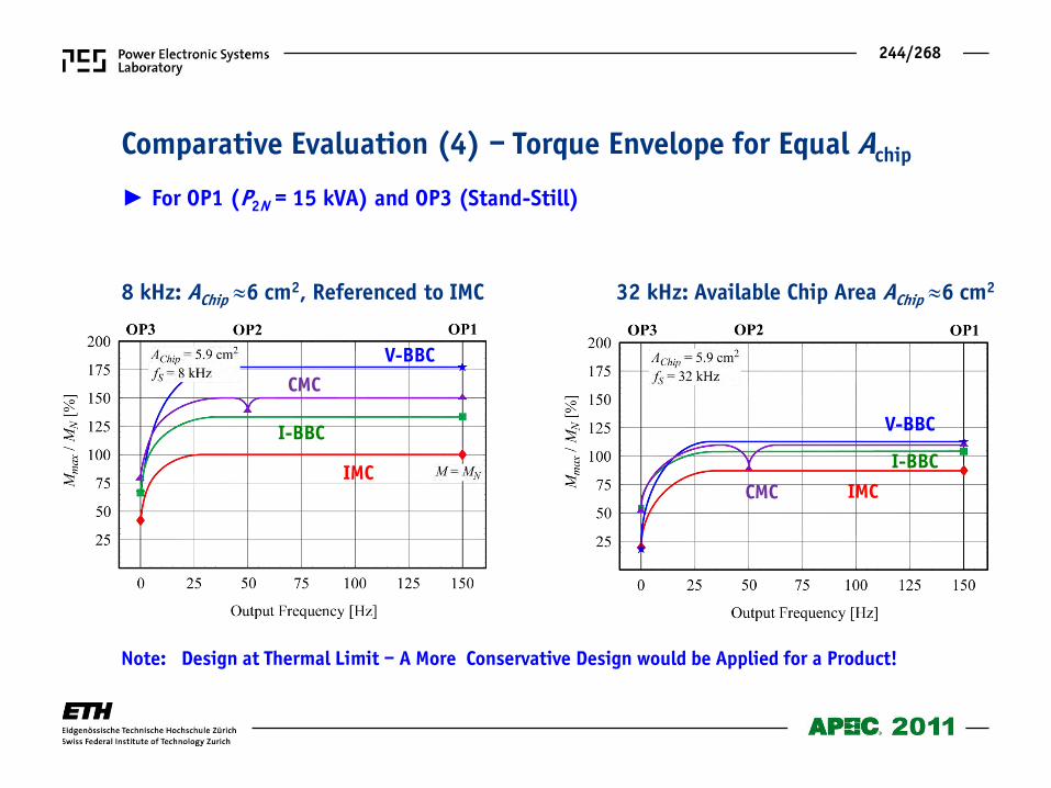
244/268
For OP1 (P2N = 15 kVA) and OP3 (Stand-Still)
Comparative Evaluation (4) – Torque Envelope for Equal Achip
8 kHz: AChip 6 cm2, Referenced to IMC 32 kHz: Available Chip Area AChip 6 cm2
CMC
V-BBC
I-BBC IMC
V-BBC
IMC
I-BBC
CMC
Note: Design at Thermal Limit – A More Conservative Design would be Applied for a Product!
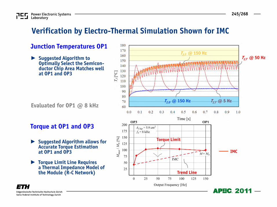
245/268
Verification by Electro-Thermal Simulation Shown for IMC
Junction Temperatures OP1
TJ,T @ 5 Hz
TJ,T @ 50 Hz TJ,T @ 150 Hz
TJ,D @ 150 Hz
Suggested Algorithm to Optimally Select the Semicon- ductor Chip Area Matches well at OP1 and OP3
Trend Line
Evaluated for OP1 @ 8 kHz
Torque Limit
Torque at OP1 and OP3
Suggested Algorithm allows for Accurate Torque Estimation at OP1 and OP3 Torque Limit Line Requires a Thermal Impedance Model of the Module (R-C Network)
IMC CMC
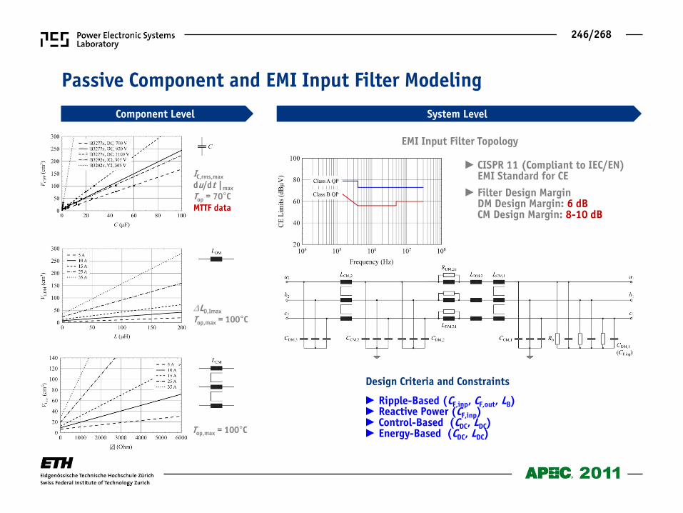
246/268
CISPR 11 (Compliant to IEC/EN) EMI Standard for CE Filter Design Margin DM Design Margin: 6 dB CM Design Margin: 8-10 dB
System Level Component Level
EMI Input Filter Topology
L0,Imax Top,max = 100°C
IC,rms,max du/dt |max Top = 70°C MTTF data
Top,max = 100°C
Ripple-Based (CF,inp, CF,out, LB) Reactive Power (CF,inp) Control-Based (CDC, LDC) Energy-Based (CDC, LDC)
Design Criteria and Constraints
Passive Component and EMI Input Filter Modeling
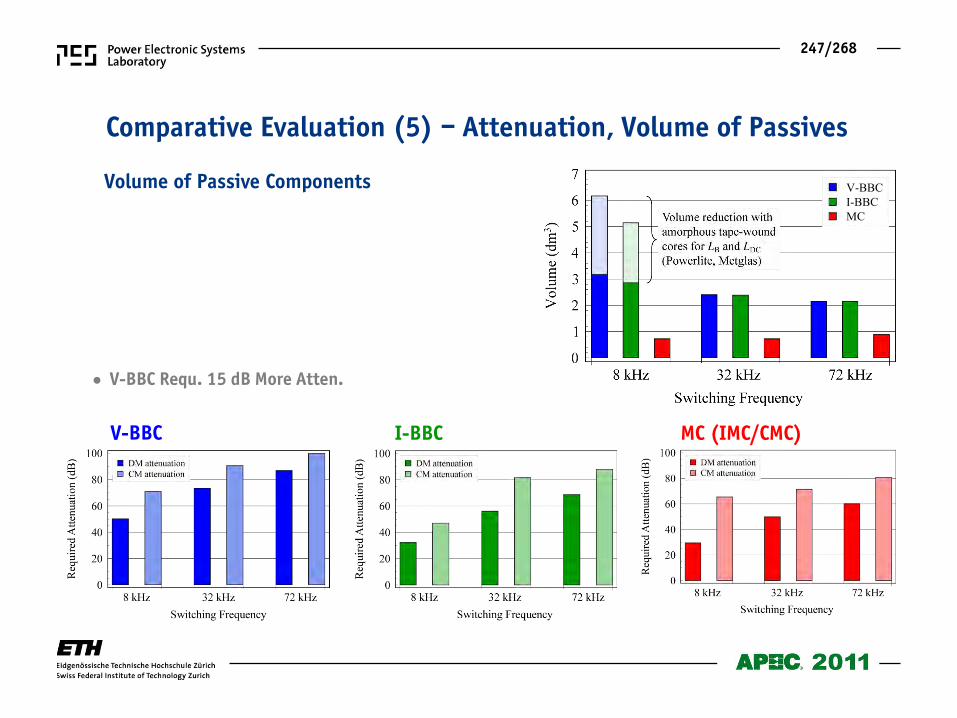
247/268
Comparative Evaluation (5) – Attenuation, Volume of Passives
Volume of Passive Components
I-BBC V-BBC MC (IMC/CMC)
V-BBC Requ. 15 dB More Atten.
V-BBC I-BBC MC
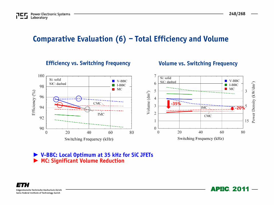
248/268
Efficiency vs. Switching Frequency Volume vs. Switching Frequency
V-BBC: Local Optimum at 35 kHz for SiC JFETs MC: Significant Volume Reduction
-35% -20%
Comparative Evaluation (6) – Total Efficiency and Volume
V-BBC I-BBC MC
V-BBC I-BBC MC

249/268
Multi-Domain Simulation Software
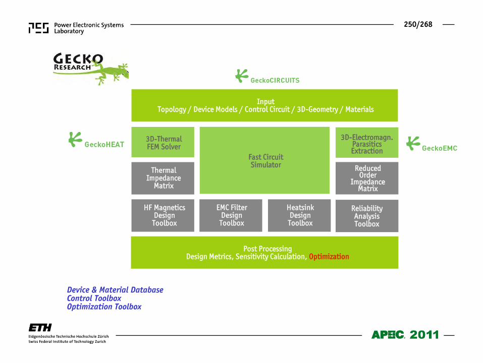
250/268
3D-Thermal FEM Solver
Thermal Impedance
Matrix
Fast Circuit Simulator
HF Magnetics Design Toolbox
3D-Electromagn. Parasitics Extraction
Reduced Order
Impedance Matrix
EMC Filter Design Toolbox
Heatsink Design Toolbox
Reliability Analysis Toolbox
Device & Material Database Control Toolbox Optimization Toolbox
Input Topology / Device Models / Control Circuit / 3D-Geometry / Materials
Post Processing Design Metrics, Sensitivity Calculation, Optimization
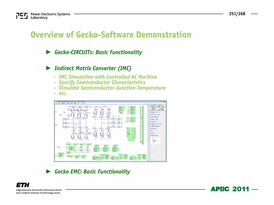
251/268
Overview of Gecko-Software Demonstration Gecko-CIRCUITs: Basic Functionality Indirect Matrix Converter (IMC)
- IMC Simulation with Controlled AC Machine - Specify Semiconductor Characteristics - Simulate Semiconductor Junction Temperature - etc. Gecko EMC: Basic Functionality
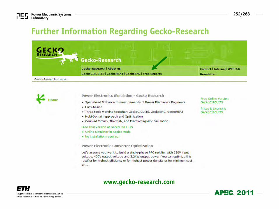
252/268
Further Information Regarding Gecko-Research
www.gecko-research.com
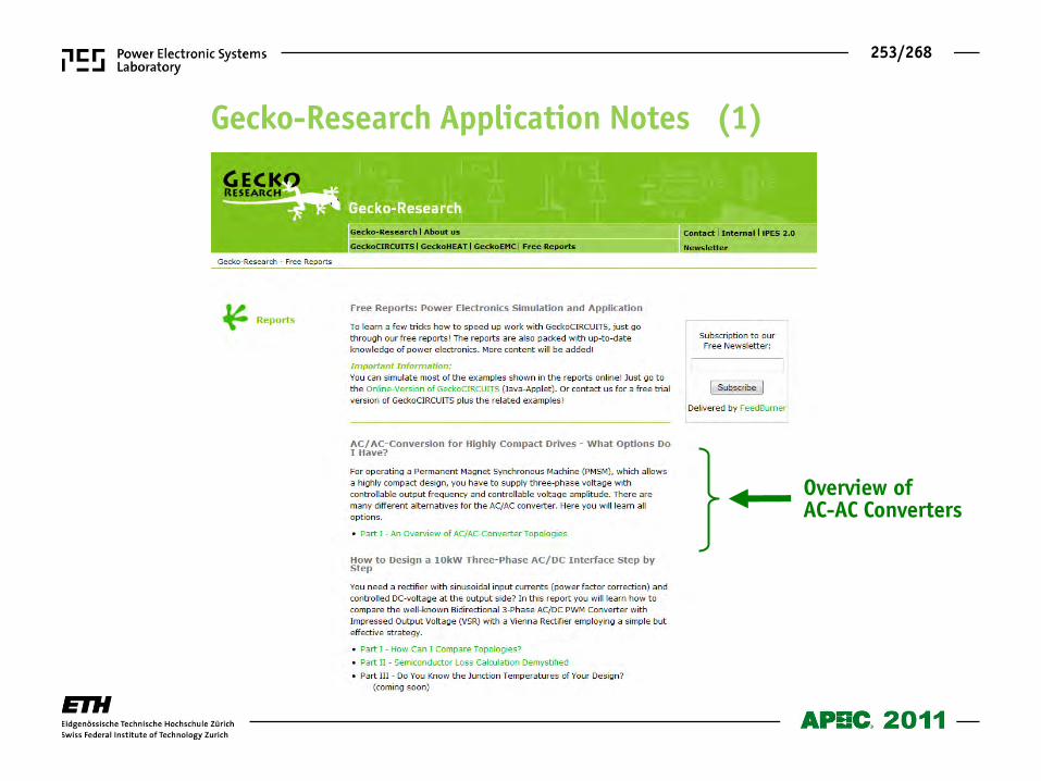
253/268
Gecko-Research Application Notes (1)
Overview of AC-AC Converters
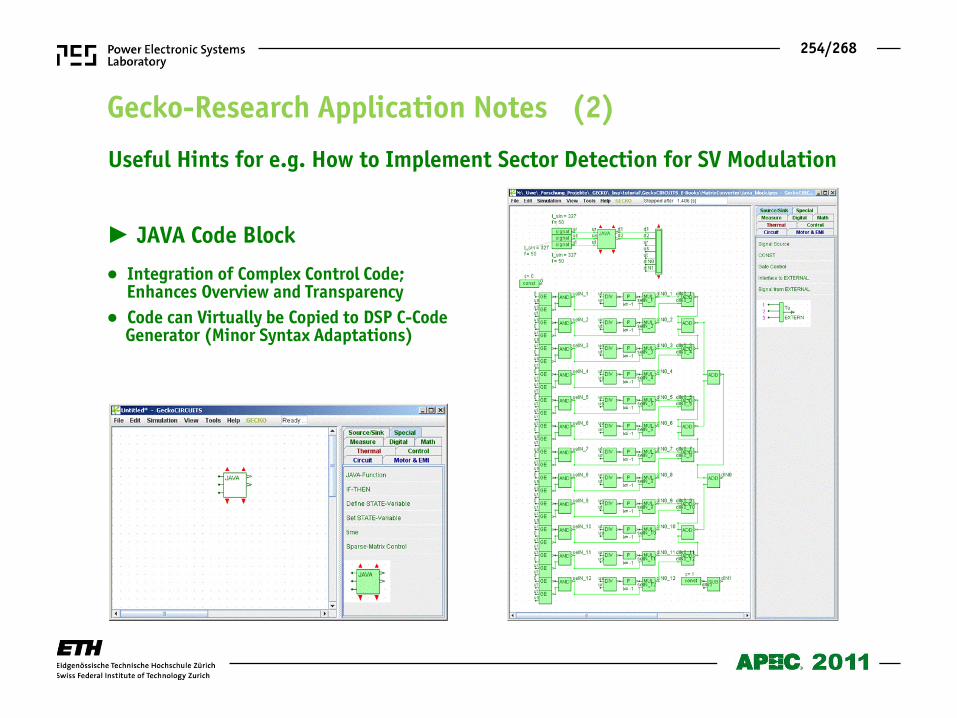
254/268
Gecko-Research Application Notes (2)
Useful Hints for e.g. How to Implement Sector Detection for SV Modulation
JAVA Code Block Integration of Complex Control Code; Enhances Overview and Transparency
Code can Virtually be Copied to DSP C-Code Generator (Minor Syntax Adaptations)
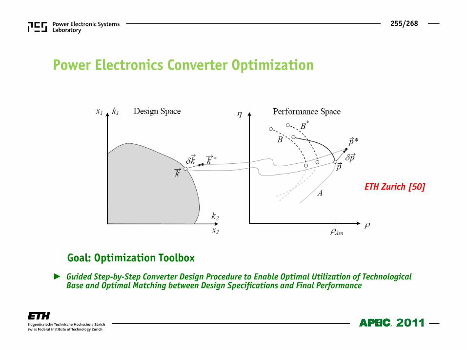
255/268
Power Electronics Converter Optimization
Goal: Optimization Toolbox Guided Step-by-Step Converter Design Procedure to Enable Optimal Utilization of Technological Base and Optimal Matching between Design Specifications and Final Performance
ETH Zurich [50]
256/268
Conclusions
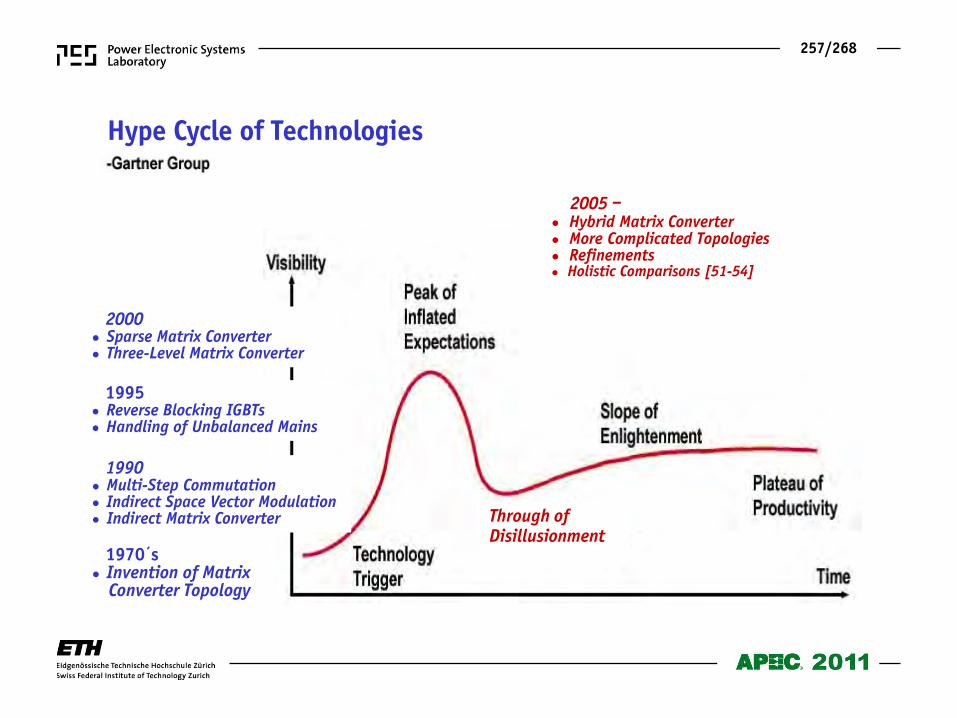
257/268
Through of Disillusionment
1970´s Invention of Matrix Converter Topology
1990 Multi-Step Commutation Indirect Space Vector Modulation Indirect Matrix Converter
1995 Reverse Blocking IGBTs Handling of Unbalanced Mains
2000 Sparse Matrix Converter Three-Level Matrix Converter
2005 – Hybrid Matrix Converter More Complicated Topologies Refinements Holistic Comparisons [51-54]
Hype Cycle of Technologies
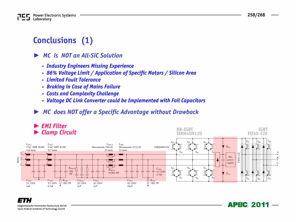
258/268
RB-IGBT IXRH40N120
IGBT FII50-12E
EMI Filter Clamp Circuit
Conclusions (1) MC is NOT an All-SiC Solution
- Industry Engineers Missing Experience - 86% Voltage Limit / Application of Specific Motors / Silicon Area - Limited Fault Tolerance - Braking in Case of Mains Failure - Costs and Complexity Challenge - Voltage DC Link Converter could be Implemented with Foil Capacitors MC does NOT offer a Specific Advantage without Drawback
CCM,1Y2 250V4.7nF
A
B
C
CDM,1X2 250V
CDM,2X2 250V
CCM,3Y2 250V1nF
CDM,2d
X2 250V
LDM,1Micrometals T132-2632 turns
LDM,1d
Micrometals T94-2622 turns
LCM,2VAC 500F W3803x7 turns
LCM,3VAC 500F W4903x4 turns
RDM,1d
RDM,2d
1W
Ma
ins
a
b
c
IXRH40N120
Sap Sbp Scp
SpcSpb
Sna Snb Snc
ScnSbnSan
FII5
0-12
E
SpA SpB SpC
SAn SBn SCn
Spa
Aux.
power
supply
Drt,n
Drt,p
RCM,1RCM,2CCM,2Y2 250V4.7nF
18 1W 18 1W
18 0.68 4W
1 F 1 F 10 F
259/268
Research MUST Address Comprehensive System Evaluations
- MC Promising for High Switching Frequency - Consider Specific Application Areas - Consider Life Cycle Costs - etc. V-BBC is a Tough Competitor F3E Might Offer a Good Compromise Most Advantageous Converter Concept Depends on Application and on whether a CUSTOM Drive Design is Possible
Integration of Multiple Functions (as for MC) Nearly ALWAYS Requires a Trade-off
Conclusions (2)
260/268
End of Part 2
261/268
Thank You !
262/268
[1] I. Takahashi and Y. Itoh, “Electrolytic Capacitor-Less PWM Inverter,“ in Proc. IPEC, Tokyo, Japan, April 2-6, 1990, pp. 131-138. [2] K. Kuusela, M. Salo, and H. Tuusa, “A Current Source PWM Converter Fed Permanent Magnet Synchronous Motor Drive with Adjustable DC-Link Current,“ in Proc. NORPIE, Aalborg, Denmark, June 15-16, 2000, pp. 54-58. [3] M.H. Bierhoff and F.W. Fuchs, “Pulse Width Modulation for Current Source Converters – A Detailed Concept,“ in Proc. IEEE Industrial Electronics Conference IECON’06, Paris, France, Nov. 7-10, 2006. [4] R.W. Erickson and O.A. Al-Naseem, “A New Family of Matrix Converters,“ in Proc. IEEE Industrial Electronics Conference IECON’01, Denver, CO, Nov. 29-Dec. 2, 2001, vol. 2, pp. 1515-1520. [5] C. Klumpner and C.I. Pitic, “Hybrid Matrix Converter Topologies: An Exploration of Benefits,“ in Proc. IEEE Power Electronics Specialists Conference PESC’08, Rhodos, Greece, June 15-19, 2008, pp. 2-8. [6] C. Klumpner, “Hybrid Direct Power Converters with Increased/Higher than Unity Voltage Transfer Ratio and Improved Robustness against Voltage Supply Disturbances,“ in Proc. IEEE Power Electronic Specialists Conference PESC’05, Recife, Brazil, June 12-16, 2005, pp. 2383-2389. [7] L. Gyugyi and B.R. Pelly, “Static Power Frequency Changers – Theory , Performance, & Application,“ New York: J. Wiley, 1976. [8] W.I. Popow, “Der zwangskommutierte Direktumrichter mit sinusförmiger Ausgangsspannung,“ Elektrie 28, no. 4, pp. 194-196, 1974. [9] K.K. Mohapatra and N. Mohan, “Open-End Winding Induction Motor Driven with Matrix Converter for Common-Mode Elimination,“ in Proc. PEDES, New Delhi, India, Dec. 12-15, 2006. [10] M. Braun and K. Hasse, “A Direct Frequency Changer with Control of Input Reactive Power,“ in Proc. 3rd IFAC Symp., Lausanne, Switzerland, 1983, pp. 187-194. [11] D.H. Shin, G.H. Cho, and S.B. Park, “Improved PWM Method of Forced Commutated Cycloconverters,“ in Proc. IEE, vol. 136, pt. B, no. 3, pp. 121-126, 1989. [12] P.D. Ziogas, Y. Kang, and V.R. Stefanovic, “Rectifier-Inverter Frequency Changers with Suppressed DC Link Components,“ IEEE Transaction on Industry Applications, vol. IA-22, no. 6, pp. 1027-1036, 1986. [13] S. Kim, S.K. Sul, and T.A. Lipo, “AC/AC Power Conversion Based on Matrix Converter Topology with Unidirectional Switches,“ IEEE Transactions on Industry Applications, vol. 36, no. 1, pp. 139-145, 2000. [14] K. Göpfrich, C. Rebbereh, and L. Sack, “Fundamental Frequency Front End Converter (F3E),“ in Proc. PCIM, Nuremberg, Germany, May 20-22, 2003, pp. 59-64.
AC-AC Converter Systems (1)
263/268
[15] B. Piepenbreier and L. Sack, “Regenerative Drive Converter with Line Frequency Switched Rectifier and Without DC Link Components,“ in Proc. IEEE Power Electronic Specialists Conference PESC’04, Aachen, Germany, June 20-25, 2004, pp. 3917-3923. [16] J. Holtz and U. Boelkens, “Direct Frequency Converter with Sinusoidal Line Currents for Speed-Variable AC Motors,“ IEEE Transactions on Industrial Electronics, vol. 36, no. 4, pp. 475-479, 1989. [17] K. Shinohara, Y. Minari, and T. Irisa, “Analysis and Fundamental Characteristics of Induction Motor Driven by Voltage Source Inverter without DC Link Components (in Japanese),“ IEEJ Transactions, vol. 109-D, no. 9, pp. 637-644, 1989. [18] L. Wei and T.A. Lipo, “A Novel Matrix Converter Topology with Simple Commutation,“ in Proc. IEEE Annual Meeting of the Industry Application Society IAS’01, Chicago, IL, Sept. 30-Oct. 4, 2001, vol. 3, pp. 1749-1754. [19] J.W. Kolar, M. Baumann, F. Stögerer, F. Schafmeister, and H. Ertl, “Novel Three-Phase AC-DC-AC Sparse Matrix Converter, Part I - Derivation, Basic Principle of Operation, Space Vector Modulation, Dimensioning, Part II - Experimental Analysis of the Very Sparse Matrix Converter,“ in Proc. IEEE Applied Power Electronic Conference APEC’01, Dallas, TX, March 10-14, 2002, vol. 2, pp. 777-791. [20] L. Wei, T.A. Lipo, and H. Chan, “Matrix Converter Topologies with Reduced Number of Switches,“ in Proc. VPEC, Blacksburg, VA, April 14-18, 2002, pp. 125-130. [21] F. Schafmeister, “Sparse und Indirekte Matrix Konverter,“ PhD Thesis no. 17428, ETH Zurich, 2007. [22] J.W. Kolar, F. Schafmeister, S.D. Round, and H. Ertl, “Novel Three-Phase AC-AC Sparse Matrix Converters,“ Transactions on Power Electronics, vol. 22, no. 5, pp. 1649-1661, 2007. [23] M.Y. Lee, P. Wheeler, and C. Klumpner, “A New Modulation Method for the Three-Level-Output-Stage Matrix Converter,“ in Proc. IEEE/IEEJ PCC, Nagoya, Japan, Apr. 2-5, 2007. [24] C. Klumpner, M. Lee, and P. Wheeler, “A New Three-Level Sparse Indirect Matrix Converter,“ in Proc. IEEE Industrial Electronics Conference IECON’06, 2006, pp. 1902-1907. [25] M. Baumann and J.W. Kolar, “Comparative Evaluation of Modulation Methods for a Three Phase / Switch Buck Power Factor Corrector Concerning the Input Capacitor Voltage Ripple,“ in Proc. IEEE Power Electronic Specialist Conference PESC’01, Vancouver, Canada, Jun. 17-21, 2001, vol. 3, pp. 1327-1333. [26] J.W. Kolar, H. Ertl, and F.C. Zach, “Power Quality Improvement of Three-Phase AC-DC Power Conversion by Discontinuous- Mode ’Dither’-Rectifier Systems,“ in Proc. International (2nd European) Power Quality Conference (PQ), Munich, Germany, Oct. 14-15, 1992, pp. 62-78. [27] J. Oyama, T. Higuchi, E. Yamada, T. Koga, and T.A. Lipo, “New Control Strategy for Matrix Converter,“ in Proc. IEEE Power Electronic Specialists Conference PESC’89, Milwaukee, WI, June 26-29, 1989, vol. 1, pp. 360-367.
AC-AC Converter Systems (2)
264/268
[28] N. Burany, “Safe Control of Four-Quadrant Switches,“ in Proc. IEEE Annual Meeting of Industry Application Society IAS’89, San Diego, CA, Oct. 1-5, 1989, pp. 1190-1194. [29] M. Ziegler and W. Hofmann, “A New Two Steps Commutation Policy for Low Cost Matrix Converter,“ in Proc. PCIM, Nuremberg, Germany, Jun. 6-8, 2000, pp. 445-450. [30] W. Hofmann and M. Ziegler, “Schaltverhalten und Beanspruchung bidirektionaler Schalter in Matrixumrichtern,“ ETG/VDE Fachbericht 88 der Fachtagung Bauelemente der Leistungselektronik, Bad Nauheim, Germany, Apr. 23-24, 2002, pp. 173-182. [31] M. Venturini, “A New Sine Wave In, Sine Wave Out Conversion Technique Eliminates Reactive Elements,“ in Proc. Powercon 7, San Diego, CA, 1980, pp. E3-1-E3-15. [32] J.W. Kolar and F.C. Zach, “A Novel Three-Phase Utility Interface Minimizing Line Current Harmonics of High-Power Telecommunications Rectifier Modules,“ Transactions on Industrial Electronics, vol. 44, no. 4, 1997, pp. 456-467. [33] J.W. Kolar, U. Drofenik, and F.C. Zach, “VIENNA Rectifier II - A Novel Single-Stage High-Frequency Isolated Three-Phase PWM Rectifier System,“ Transactions on Industrial Electronics, vol. 46, no. 4, pp. 674-691, 1999. [34] K. Mino, Y. Okuma, and K. Kuroki, “Direct-Linked-Type Frequency Changer Based on DC-Clamped Bilateral Switching Circuit Topology,“ Transactions on Industrial Electronics, vol. 34, no. 6, pp. 1309-1317, 1998. [35] D. Casadei, G. Serra, A. Tani, and P. Nielsen, “Performance of SVM Controlled Matrix Converter with Input and Output Unbalanced Condition,“ in Proc. European Conference on Power Electronics and Applications EPE’95, Sevilla, Spain, Sept. 19-21, 1995, vol. 2, pp. 628-633. [36] F. Schafmeister, M. Baumann, and J.W. Kolar, “Analytically Closed Calculation of the Conduction and Switching Losses of Three-Phase AC-AC Sparse Matrix Converters,” in Proc. International Power Electronics and Motion Control Conference, Dubrovnik, Croatia, Sept. 9-11, 2002, CD-ROM, ISBN: 953-184-047-4. [37] F. Schafmeister, S. Herold, and J.W. Kolar, “Evaluation of 1200V-Si-IGBTs and 1300V-SiC-JFETs for Application in Three- Phase Very Sparse Matrix AC-AC Converter Systems,” in Proc. IEEE Applied Power Electronics Conference and Exposition, Miami Beach, USA, Feb. 9-13, vol. 1, pp. 241-255, 2003. [38] J.W. Kolar and F. Schafmeister, “Novel Modulation Schemes Minimizing the Switching Losses of Sparse Matrix Converters,” in Proc. IEEE Industrial Electronics Society Conference IECON’03, Roanoke, USA, Nov. 2-6, 2003, pp. 2085-2090. [39] M.L. Heldwein, T. Nussbaumer, and J.W. Kolar, “Differential Mode EMC Input Filter Design for Three-Phase AC-DC-AC Sparse Matrix PWM Converters,” in Proc. IEEE Power Electronics Specialists Conference, Aachen, Germany, June 20-25, 2004, CD-ROM, ISBN: 07803-8400-8.
AC-AC Converter Systems (3)
265/268
[40] M.L. Heldwein, T. Nussbaumer, F. Beck, and J.W. Kolar, “Novel Three-Phase CM/DM Conducted Emissions Separator,” in Proc. IEEE Applied Power Electronics Conference and Exposition, Austin (Texas), USA, March 6-10, 2005, vol. 2, pp. 797-802. [41] T. Friedli, M.L. Heldwein, F. Giezendanner, and J.W. Kolar, “A High Efficiency Indirect Matrix Converter Utilizing RB-IGBTs,” in Proc. IEEE Power Electronics Specialists Conference PESC’06, Jeju, Korea, Jun. 18-22, 2006, CD-ROM, ISBN: 1-4244-9717-7. [42] S. Round, F. Schafmeister, M.L. Heldwein, E. Pereira, L. Serpa, and J.W. Kolar, “Comparison of Performance and Realization Effort of a Very Sparse Matrix Converter to a Voltage DC Link PWM Inverter with Active Front End,” IEEJ Transactions of the Institute of Electrical Engineers of Japan, vol. 126-D, no. 5, May 2006, pp. 578-588. [43] T. Friedli, S.D. Round, D. Hassler, J.W. Kolar, “Design and Performance of a 200 kHz All-SiC JFET Current DC-Link Back- to-Back Converter”, IEEE Transactions on Industry Applications, vol. 45, no. 5, Sept./Oct. 2009, pp.1868-1878. [44] F.Z. Peng, A. Joseph, J. Wang, M. Shen, L. Chen, Z. Pan, E. Ortiz-Rivera, Y. Huang, “Z-Source Inverter for Motor Drives”, IEEE Transactions on Power Electronics, vol. 20, no. 4, Jul. 2005, pp. 857-863. [45] L. Sack, B. Piepenbreier, M. von Zimmermann, “Dimensioning of the Z-Source Inverter for General Purpose Drives with Three-Phase Standard Motors”, in Proc. Power Electronic Specialist Conference, Rhodes, Greece, Jun. 5-19, 2008, pp. 1808-1813. [46] R. Strzelecki, M. Adamowicz, N. Strzelecka, W. Bury, “New Type T-Source Inverter”, in Proc. Power Quality Alternative Energy and Distributed Systems, Badajoz, Spain, May 20-22, 2009, pp. 191-195. [47] D. Cottet, U. Drofenik, J.-M. Meyer, “A Systematic Design Approach to Thermal-Electrical Power Electronics Integration”, Electronics System Integration Conference ESTC’08, Greenwich, UK, Sept. 1-4, 2007, pp. 219-224. [48] W. Qian, F.Z. Peng, H. Cha, “Trans-Z-Source Inverters”, Proc. IEEE/IEEJ International Power Electronics Conference (ECCE Asia) IPEC’10, Sapporo, Japan, Jun. 21-24, 2010, pp. 1874-1881. [49] T. Friedli and J.W. Kolar, “A Semiconductor Area Based Assessment of AC Motor Drive Converter Topologies”, Proc. IEEE Applied Power Electronic Conference and Exhibition APEC’09, Washington DC, USA, Feb. 15-19, pp. 336-342. [50] J.W. Kolar, J. Biela, and J. Miniböck, “Exploring the Pareto Front of Multi-Objective Single-Phase PFC Rectifier Design Optimization – 99.2% Efficiency vs. 7 kW/dm3 Power Density”, in Proc. IEEE International Power Electronics and Motion IPEMC’09, Wuhan, China, May 17-20, 2009, CD-ROM.
AC-AC Converter Systems (5)
266/268
[51] S. Bernet, S. Ponnaluri, and R. Teichmann , “Design and Loss Comparison of Matrix Converters and Voltage-Source Converters for Modern AC Drives”, IEEE Transactions on Industrial Electronics, vol. 49, no. 2, April 2002, pp. 304-314. [52] R. Lai, Y. Pei, F. Wang, R. Burgos, D. Boroyevich, T.A. Lipo, V. Immanuel, K. Karimi, “A Systematic Evaluation of AC- Fed Converter Topologies for Light Weight Motor Drive Applications Using SiC Semiconductor Devices”, in Proc. Electric Machines and Drives Conference IEMDC’07, Antalya, Turkey, May 3-5, 2007, pp. 1300-1305. [53] T. Friedli and J.W. Kolar, “Comprehensive Comparison of Three-Phase AC-AC Matrix Converter and Voltage DC-Link Back-to- Back Converter Systems”, Invited Paper, Proc. IEEE/IEEJ International Power Electronics Conference (ECCE Asia) IPEC’10, Sapporo, Japan, Jun. 21-24, 2010, pp. 2789-2798. [54] M. Schweizer, I. Lizama, T. Friedli, and J.W. Kolar, “Comparison of the Chip Area Usage of 2-level and 3-level Voltage Source Converter Topologies”, Proc. IEEE Industrial Electronics Conference IECON’10, Glendale, USA, Nov. 7-11, 2010.
AC-AC Converter Systems (6)
267/268
Johann W. Kolar (F´10) received his Ph.D. degree (summa cum laude / promotio sub auspiciis praesidentis rei publicae) from the University of Technology Vienna, Austria. Since 1984 he has been working as an independent international consultant in close collaboration with the University of Technology Vienna, in the fields of power electronics, industrial electronics and high performance drives. He has proposed numerous novel PWM converter topologies, and modulation and control concepts, e.g., the VIENNA Rectifier and the Three-Phase AC-AC Sparse Matrix Converter. Dr. Kolar has published over 350 scientific papers in international journals and conference proceedings and has filed 75 patents. He was appointed Professor and Head of the Power Electronic Systems Laboratory at the Swiss Federal Institute of Technology (ETH) Zurich on Feb. 1, 2001.
The focus of his current research is on AC-AC and AC-DC converter topologies with low effects on the mains, e.g. for power supply of data centers, More-Electric-Aircraft and distributed renewable energy systems. Further main areas of research are the realization of ultra-compact and ultra-efficient converter modules employing latest power semiconductor technology (SiC), novel concepts for cooling and EMI filtering, multi-domain/multi-scale modeling / simulation and multi-objective optimization, physical model based lifetime prediction, pulsed power, bearingless motors, and Power MEMS.
He received the Best Transactions Paper Award of the IEEE Industrial Electronics Society in 2005, the Best Paper Award of the ICPE in 2007, the 1st Prize Paper Award of the IEEE IAS IPCC in 2008, and the IEEE IECON Best Paper Award of the IES PETC in 2009. He also received an Erskine Fellowship from the University of Canterbury, New Zealand, in 2003. He initiated and/or is the founder / co-founder of 4 Spin-off Companies targeting ultra high speed drives, multi-domain/level simulation, ultra-compact/efficient converter systems and pulsed power/electronic energy processing. In 2006, the European Power Supplies Manufacturers Association (EPSMA) awarded the Power Electronics Systems Laboratory of ETH Zurich as the leading academic research institution in Power Electronics in Europe.
Dr. Kolar is a Fellow of the IEEE and a Member of the IEEJ and of International Steering Committees and Technical Program Committees of numerous international conferences in the field (e.g. Director of the Power Quality Branch of the International Conference on Power Conversion and Intelligent Motion). He is the founding Chairman of the IEEE PELS Austria and Switzerland Chapter and Chairman of the Education Chapter of the EPE Association. From 1997 through 2000 he has been serving as an Associate Editor of the IEEE Transactions on Industrial Electronics and since 2001 as an Associate Editor of the IEEE Transactions on Power Electronics. Since 2002 he also is an Associate Editor of the Journal of Power Electronics of the Korean Institute of Power Electronics and a member of the Editorial Advisory Board of the IEEJ Transactions on Electrical and Electronic Engineering.
About the Instructors
268/268
Thomas Friedli (M’09) received his M.Sc. degree in electrical engineering and information technology (with distinction) and his Ph.D. from the Swiss Federal Institute of Technology (ETH) Zurich, in 2005 and 2010, respectively. From 2003 to 2004 he worked as a trainee for Power-One in the R&D centre for telecom power supplies. His Ph.D. research from 2006 to 2009 involved the further development of current source and matrix converter topologies in collaboration with industry using silicon carbide JFETs and diodes and a comparative evaluation of three-phase ac-ac converter systems. He received the 1st Prize Paper Award of the IEEE IAS IPCC in 2008 and the IEEE IAS Transactions Prize Paper Award in 2009.
Michael Hartmann (M’09) was born in Feldkirch, Austria, on May 26, 1978. After he finished the HTL-Rankweil (Telecommunications), he started to work at Omicron Electronics in Klaus (Austria) as a hardware development engineer. There, his work was focused on measurements techniques for power system testing.
In October 2001, he began to study electrical engineering at the University of Technology Vienna, Austria. His diploma thesis deals with the design and implementation of a multi-cell switch mode power amplifier with zero-voltage switching DC-links employing a digital modulator. He received his M.Sc. degree with honors in November 2006, and he has been a Ph.D. student at the Power Electronic Systems Laboratory, ETH Zürich, since March 2007.