Thin Film Polycrystalline Silicon Nanowire Biosensors · PDF fileare needed and 100 nm...
5
Thin Film Polycrystalline Silicon Nanowire Biosensors Mohammad M. A. Hakim,* ,†,⊥ Marta Lombardini,* ,†,‡,⊥ Kai Sun, † Francesco Giustiniano, § Peter L. Roach, § Donna E. Davies, ∥ Peter H. Howarth, ∥ Maurits R. R. de Planque, †,‡ Hywel Morgan, †,‡ and Peter Ashburn † † School of Electronics & Computer Science, University of Southampton, Southampton, SO17 1BJ, U.K. ‡ Institute for Life Sciences, University of Southampton, Southampton, SO17 1BJ, U.K. § School of Chemistry, University of Southampton, Southampton, SO17 1BJ, U.K. ∥ Clinical and Experimental Sciences, Faculty of Medicine, University of Southampton, Southampton General Hospital, Southampton, SO16 6YD, U.K. * S Supporting Information ABSTRACT: Polysilicon nanowire biosensors have been fabricated using a top-down process and were used to determine the binding constant of two inflammatory biomarkers. A very low cost nano- fabrication process was developed, based on simple and mature photolithography, thin film technology, and plasma etching, enabling an easy route to mass manufacture. Antibody-functionalized nanowire sensors were used to detect the proteins interleukin-8 (IL-8) and tumor necrosis factor-alpha (TNF-α) over a wide range of concentrations, demonstrating excellent sensitivity and selectivity, exemplified by a detection sensitivity of 10 fM in the presence of a 100 000-fold excess of a nontarget protein. Nanowire titration curves gave antibody−antigen dissociation constants in good agreement with low-salt enzyme-linked immunosorbent assays (ELISAs). This fabrication process produces high-quality nanowires that are suitable for low-cost mass production, providing a realistic route to the realization of disposable nanoelectronic point-of-care (PoC) devices. KEYWORDS: Nanowires, silicon, cytokines, binding constant, immunoassay, point of care O ver the past decade, silicon nanowires have emerged as important candidates for biochemical sensors. 1−6 There are many reasons why silicon nanowires are of interest, including high surface-to-volume ratio, high sensitivity, and real-time, label-free detection without expensive optical components. 1 Although nanowire field effect transistors have been used to sense ions, proteins, DNA, and viruses, outstanding issues remain, most notably the cost and practicality of fabrication. Therefore, the development of a very low-cost and simple fabrication route suitable for mass manufacture of disposable nanowire sensors would accelerate their uptake as point-of-care (PoC) devices. Validation of nanowire biosensors against standard enzyme-linked immuno- sorbent assays (ELISAs), including a characterization of binding kinetics, is an additional requirement for further development of these systems. 2,7 There are two major approaches for fabricating nanowire biosensors, namely, top-down and bottom-up. Bottom-up approaches usually involve metal-catalytic nanowire growth, 8 which is simple and cheap and produces uniformly sized single- crystal nanowires, followed by an integration step such as electric field or fluid-flow-assisted nanowire positioning between lithographically defined source and drain electrodes. 9 However, this introduces an additional (non-CMOS) device fabrication step and does not provide the precise control over nanowire position provided by lithographically defined nano- wires. 9 Top-down approaches overcome these shortcomings, and several groups have used nanopatterning techniques such as deep-UV 10 lithography (steppers) and electron beam lithography 11,12 to fabricate silicon nanowires on silicon-on- insulator (SOI) substrates. This has the advantage of CMOS compatibility, but a serious disadvantage is the high cost associated with these advanced lithography techniques and expensive SOI wafers. To achieve a minimum feature size below 90 nm on a wafer scale, an enormous engineering effort has been expended to evolve stepper technology from the 365 nm mercury lamp to the 13.4 nm extreme ultraviolet regime. 13−15 However, each successive stepper technology is more costly due to the requirement for more expensive optics and light sources. Furthermore, the cost of mask manufacture is also escalating, forcing chip designers to amortize design and mask expenses across the largest possible volume. Wet etch of SOI wafers has also been researched as a means of creating Received: December 1, 2011 Revised: February 22, 2012 Published: March 20, 2012 Letter pubs.acs.org/NanoLett © 2012 American Chemical Society 1868 dx.doi.org/10.1021/nl2042276 | Nano Lett. 2012, 12, 1868−1872
Transcript of Thin Film Polycrystalline Silicon Nanowire Biosensors · PDF fileare needed and 100 nm...

Thin Film Polycrystalline Silicon Nanowire BiosensorsMohammad M. A. Hakim,*,†,⊥ Marta Lombardini,*,†,‡,⊥ Kai Sun,† Francesco Giustiniano,§
Peter L. Roach,§ Donna E. Davies,∥ Peter H. Howarth,∥ Maurits R. R. de Planque,†,‡ Hywel Morgan,†,‡
and Peter Ashburn†
†School of Electronics & Computer Science, University of Southampton, Southampton, SO17 1BJ, U.K.‡Institute for Life Sciences, University of Southampton, Southampton, SO17 1BJ, U.K.§School of Chemistry, University of Southampton, Southampton, SO17 1BJ, U.K.∥Clinical and Experimental Sciences, Faculty of Medicine, University of Southampton, Southampton General Hospital, Southampton,SO16 6YD, U.K.
*S Supporting Information
ABSTRACT: Polysilicon nanowire biosensors have been fabricatedusing a top-down process and were used to determine the bindingconstant of two inflammatory biomarkers. A very low cost nano-fabrication process was developed, based on simple and maturephotolithography, thin film technology, and plasma etching, enablingan easy route to mass manufacture. Antibody-functionalized nanowiresensors were used to detect the proteins interleukin-8 (IL-8) and tumornecrosis factor-alpha (TNF-α) over a wide range of concentrations,demonstrating excellent sensitivity and selectivity, exemplified by adetection sensitivity of 10 fM in the presence of a 100 000-fold excess ofa nontarget protein. Nanowire titration curves gave antibody−antigendissociation constants in good agreement with low-salt enzyme-linkedimmunosorbent assays (ELISAs). This fabrication process produceshigh-quality nanowires that are suitable for low-cost mass production, providing a realistic route to the realization of disposablenanoelectronic point-of-care (PoC) devices.
KEYWORDS: Nanowires, silicon, cytokines, binding constant, immunoassay, point of care
Over the past decade, silicon nanowires have emerged asimportant candidates for biochemical sensors.1−6 There
are many reasons why silicon nanowires are of interest,including high surface-to-volume ratio, high sensitivity, andreal-time, label-free detection without expensive opticalcomponents.1 Although nanowire field effect transistors havebeen used to sense ions, proteins, DNA, and viruses,outstanding issues remain, most notably the cost andpracticality of fabrication. Therefore, the development of avery low-cost and simple fabrication route suitable for massmanufacture of disposable nanowire sensors would acceleratetheir uptake as point-of-care (PoC) devices. Validation ofnanowire biosensors against standard enzyme-linked immuno-sorbent assays (ELISAs), including a characterization of bindingkinetics, is an additional requirement for further developmentof these systems.2,7
There are two major approaches for fabricating nanowirebiosensors, namely, top-down and bottom-up. Bottom-upapproaches usually involve metal-catalytic nanowire growth,8
which is simple and cheap and produces uniformly sized single-crystal nanowires, followed by an integration step such aselectric field or fluid-flow-assisted nanowire positioningbetween lithographically defined source and drain electrodes.9
However, this introduces an additional (non-CMOS) device
fabrication step and does not provide the precise control overnanowire position provided by lithographically defined nano-wires.9 Top-down approaches overcome these shortcomings,and several groups have used nanopatterning techniques suchas deep-UV10 lithography (steppers) and electron beamlithography11,12 to fabricate silicon nanowires on silicon-on-insulator (SOI) substrates. This has the advantage of CMOScompatibility, but a serious disadvantage is the high costassociated with these advanced lithography techniques andexpensive SOI wafers. To achieve a minimum feature sizebelow 90 nm on a wafer scale, an enormous engineering efforthas been expended to evolve stepper technology from the 365nm mercury lamp to the 13.4 nm extreme ultravioletregime.13−15 However, each successive stepper technology ismore costly due to the requirement for more expensive opticsand light sources. Furthermore, the cost of mask manufacture isalso escalating, forcing chip designers to amortize design andmask expenses across the largest possible volume. Wet etch ofSOI wafers has also been researched as a means of creating
Received: December 1, 2011Revised: February 22, 2012Published: March 20, 2012
Letter
pubs.acs.org/NanoLett
© 2012 American Chemical Society 1868 dx.doi.org/10.1021/nl2042276 | Nano Lett. 2012, 12, 1868−1872

triangular nanowires without the need for advanced litho-graphy,16,17 but as wet etching is not favored by industry, thisapproach does not provide a clear route to manufacturing.Recently, a low cost, top-down approach to nanowirefabrication has been reported that uses thin film technologyand the spacer etch technique.18−20 This approach isparticularly attractive because it produces polysilicon nanowireswith nanoscale dimensions using mature lithography incombination with standard deposition and spacer etch
techniques that are widely available in industry. However, themain disadvantage is that the nanowires are shaped as a quartercircle due to the absence of mask protection, which makes itdifficult to control the cross-sectional area and hence thesensitivity of the nanowires.In this paper, rectangular nanowires are fabricated using a
novel spacer etch process with a thin film technology similar tothat used for the manufacture of thin film transistor (TFT)displays. Using this approach, no expensive lithography tools
Figure 1. Schematic illustrations of polysilicon nanowire biosensor fabrication after (a) oxide pillar formation, (b) nanowire plasma etch, (c) metalcontact formation, and (d) sensor window opening. The biasing configuration for the biosensor electrical measurements is also shown: (e) cross-sectional SEM image of a fabricated polysilicon nanowire; (f) cross-sectional SEM micrograph of polysilicon nanowires at the corner of a pillar; (g)optical image of a completed nanowire biosensor wafer; (h) high magnification optical image of a fabricated nanowire biosensor through a sensorwindow.
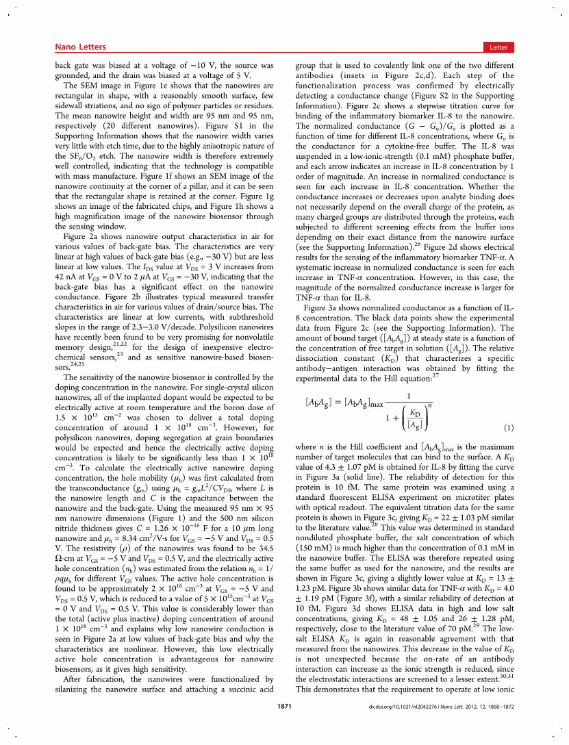
Figure 2. Polysilicon nanowire electrical characterization in air and in solution: (a) polysilicon nanowire output characteristic (IDS as a function ofVDS for different VGS values) measured in air; (b) polysilicon nanowire transfer characteristic (ln IDS as a function of VGS for different VDS values)measured in air; (c) normalized conduction change as a function of time showing the real-time detection of different concentrations of IL-8; (d)normalized conduction change as a function of time showing the real-time detection of different concentrations of TNF-α . The numbers 1−7indicate the time at which the concentration of IL-8 or TNF-α is increased by 1 order of magnitude, starting from 10 fM.
Nano Letters Letter
dx.doi.org/10.1021/nl2042276 | Nano Lett. 2012, 12, 1868−18721869

are needed and 100 nm nanowires can be fabricated using asimple thin film technology. Rectangular polycrystalline silicon(polysilicon) nanowires are defined by deposition andanisotropic etch using low cost reactive ion etch (RIE)equipment and mature 3 μm lithography, delivering excellentcontrol of the nanowire width and shape. Furthermore, theprocess can be up-scaled to produce nanowires on a very largescale similar to the production of flat screen displays. Antibody-functionalized nanowire sensors are fabricated and used togenerate titration curves for the proteins interleukin-8 (IL-8)and tumor necrosis factor-alpha (TNF-α) over a wide range ofconcentrations.The nanowire biosensor fabrication starts with deposition of
a 100 nm low pressure chemical vapor deposited (LPCVD)amorphous silicon (α-Si) film over a silicon dioxide pillar. Theoxide pillars are created by depositing a plasma enhancedchemical vapor deposited (PECVD) oxide layer, patterning
using 3 μm photolithography and anisotropic etching (Figure1a). The α-Si film was deposited at 560 °C and doped by boronimplantation at a dose of 1.5 × 10¹³/cm2 and an energy of 25keV. Nanowires were formed (Figure 1b) using an OxfordInstruments Plasma Technology system 80+ reactive ion etcherusing a highly anisotropic etch, with a SF6 flow of 12 sccm, anO2 flow of 12 sccm, a pressure of 30 mT, and an RIE power of160 W. A 10 nm gate oxide was then grown at 900 °C to createa stable surface for nanowire functionalization, to crystallize theamorphous silicon to polycrystalline silicon, and to activate theimplanted dopant. Aluminum contacts (Figure 1c) to eitherend of the polysilicon nanowire were made via heavily dopedsource/drain pads, and a sensing window was opened over thenanowires in a deposited insulator (Figure 1d). The siliconsubstrate acts as a back gate, allowing the nanowire conductivityto be modulated through the application of a back gate bias(Figure 1d). When performing biosensor measurements, the
Figure 3. Polysilicon nanowire biosensor results: (a) titration curve of the reaction of IL-8 in a polysilicon nanowire biosensor (the extracted value ofKD is 4.3 pM); (b) titration curve of the reaction of TNF-α in a polysilicon nanowire biosensor (the extracted value of KD is 4.0 pM); (c) detectionof IL-8 using an ELISA assay at two different salt concentrations (the KD obtained from the titration curve of the standard ELISA (square symbols) is23 pM, while that obtained from the low salt ELISA (round symbols) gives 13 pM); (d) the detection of TNF-α using an ELISA assay at twodifferent salt concentrations (the KD obtained from the titration curve of the standard ELISA (square symbols) is 48 pM, while that obtained fromthe low-salt ELISA (round symbols) gives 26 pM); (e) comparison of the sensitivity of an anti-IL-8 functionalized nanowire when detecting a lowconcentration (10 fM) of its specific target IL-8 and a high concentration of a nonspecific protein (1 nM TNF-α); (f) comparison of the sensitivityof an anti-TNF-α functionalized nanowire when detecting a low concentration (10 fM) of its specific target TNF-α and a high concentration of anontarget protein (1 nM IL-8).
Nano Letters Letter
dx.doi.org/10.1021/nl2042276 | Nano Lett. 2012, 12, 1868−18721870
back gate was biased at a voltage of −10 V, the source wasgrounded, and the drain was biased at a voltage of 5 V.The SEM image in Figure 1e shows that the nanowires are
rectangular in shape, with a reasonably smooth surface, fewsidewall striations, and no sign of polymer particles or residues.The mean nanowire height and width are 95 nm and 95 nm,respectively (20 different nanowires). Figure S1 in theSupporting Information shows that the nanowire width variesvery little with etch time, due to the highly anisotropic nature ofthe SF6/O2 etch. The nanowire width is therefore extremelywell controlled, indicating that the technology is compatiblewith mass manufacture. Figure 1f shows an SEM image of thenanowire continuity at the corner of a pillar, and it can be seenthat the rectangular shape is retained at the corner. Figure 1gshows an image of the fabricated chips, and Figure 1h shows ahigh magnification image of the nanowire biosensor throughthe sensing window.Figure 2a shows nanowire output characteristics in air for
various values of back-gate bias. The characteristics are verylinear at high values of back-gate bias (e.g., −30 V) but are lesslinear at low values. The IDS value at VDS = 3 V increases from42 nA at VGS = 0 V to 2 μA at VGS = −30 V, indicating that theback-gate bias has a significant effect on the nanowireconductance. Figure 2b illustrates typical measured transfercharacteristics in air for various values of drain/source bias. Thecharacteristics are linear at low currents, with subthresholdslopes in the range of 2.3−3.0 V/decade. Polysilicon nanowireshave recently been found to be very promising for nonvolatilememory design,21,22 for the design of inexpensive electro-chemical sensors,23 and as sensitive nanowire-based biosen-sors.24,25
The sensitivity of the nanowire biosensor is controlled by thedoping concentration in the nanowire. For single-crystal siliconnanowires, all of the implanted dopant would be expected to beelectrically active at room temperature and the boron dose of1.5 × 1013 cm−2 was chosen to deliver a total dopingconcentration of around 1 × 1018 cm−3. However, forpolysilicon nanowires, doping segregation at grain boundarieswould be expected and hence the electrically active dopingconcentration is likely to be significantly less than 1 × 10¹⁸
cm−3. To calculate the electrically active nanowire dopingconcentration, the hole mobility (μh) was first calculated fromthe transconductance (gm) using μh = gmL
2/CVDS, where L isthe nanowire length and C is the capacitance between thenanowire and the back-gate. Using the measured 95 nm × 95nm nanowire dimensions (Figure 1) and the 500 nm siliconnitride thickness gives C = 1.26 × 10⁻¹⁶ F for a 10 μm longnanowire and μh = 8.34 cm2/V·s for VGS = −5 V and VDS = 0.5V. The resistivity (ρ) of the nanowires was found to be 34.5Ω·cm at VGS = −5 V and VDS = 0.5 V, and the electrically activehole concentration (nh) was estimated from the relation nh = 1/ρqμh for different VGS values. The active hole concentration isfound to be approximately 2 × 1016 cm−3 at VGS = −5 V andVDS = 0.5 V, which is reduced to a value of 5 × 1015cm−3 at VGS= 0 V and VDS = 0.5 V. This value is considerably lower thanthe total (active plus inactive) doping concentration of around1 × 1018 cm−3 and explains why low nanowire conduction isseen in Figure 2a at low values of back-gate bias and why thecharacteristics are nonlinear. However, this low electricallyactive hole concentration is advantageous for nanowirebiosensors, as it gives high sensitivity.After fabrication, the nanowires were functionalized by
silanizing the nanowire surface and attaching a succinic acid
group that is used to covalently link one of the two differentantibodies (insets in Figure 2c,d). Each step of thefunctionalization process was confirmed by electricallydetecting a conductance change (Figure S2 in the SupportingInformation). Figure 2c shows a stepwise titration curve forbinding of the inflammatory biomarker IL-8 to the nanowire.The normalized conductance (G − Go)/Go is plotted as afunction of time for different IL-8 concentrations, where Go isthe conductance for a cytokine-free buffer. The IL-8 wassuspended in a low-ionic-strength (0.1 mM) phosphate buffer,and each arrow indicates an increase in IL-8 concentration by 1order of magnitude. An increase in normalized conductance isseen for each increase in IL-8 concentration. Whether theconductance increases or decreases upon analyte binding doesnot necessarily depend on the overall charge of the protein, asmany charged groups are distributed through the proteins, eachsubjected to different screening effects from the buffer ionsdepending on their exact distance from the nanowire surface(see the Supporting Information).26 Figure 2d shows electricalresults for the sensing of the inflammatory biomarker TNF-α. Asystematic increase in normalized conductance is seen for eachincrease in TNF-α concentration. However, in this case, themagnitude of the normalized conductance increase is larger forTNF-α than for IL-8.Figure 3a shows normalized conductance as a function of IL-
8 concentration. The black data points show the experimentaldata from Figure 2c (see the Supporting Information). Theamount of bound target ([AbAg]) at steady state is a function ofthe concentration of free target in solution ([Ag]). The relativedissociation constant (KD) that characterizes a specificantibody−antigen interaction was obtained by fitting theexperimental data to the Hill equation:27
=
+⎛⎝⎜⎜
⎞⎠⎟⎟
A A A A[ ] [ ]1
1KA
nb g b g max
[ ]D
g (1)
where n is the Hill coefficient and [AbAg]max is the maximumnumber of target molecules that can bind to the surface. A KDvalue of 4.3 ± 1.07 pM is obtained for IL-8 by fitting the curvein Figure 3a (solid line). The reliability of detection for thisprotein is 10 fM. The same protein was examined using astandard fluorescent ELISA experiment on microtiter plateswith optical readout. The equivalent titration data for the sameprotein is shown in Figure 3c, giving KD = 22 ± 1.03 pM similarto the literature value.28 This value was determined in standardnondiluted phosphate buffer, the salt concentration of which(150 mM) is much higher than the concentration of 0.1 mM inthe nanowire buffer. The ELISA was therefore repeated usingthe same buffer as used for the nanowire, and the results areshown in Figure 3c, giving a slightly lower value at KD = 13 ±1.23 pM. Figure 3b shows similar data for TNF-α with KD = 4.0± 1.19 pM (Figure 3f), with a similar reliability of detection at10 fM. Figure 3d shows ELISA data in high and low saltconcentrations, giving KD = 48 ± 1.05 and 26 ± 1.28 pM,respectively, close to the literature value of 70 pM.29 The low-salt ELISA KD is again in reasonable agreement with thatmeasured from the nanowires. This decrease in the value of KDis not unexpected because the on-rate of an antibodyinteraction can increase as the ionic strength is reduced, sincethe electrostatic interactions are screened to a lesser extent.30,31
This demonstrates that the requirement to operate at low ionic
Nano Letters Letter
dx.doi.org/10.1021/nl2042276 | Nano Lett. 2012, 12, 1868−18721871

strength is not perturbing the antibody binding constant in asignificant way.The selectivity of this nanowire assay was investigated by
comparing the cross-reactivity of two nanowires functionalizedwith the two different antibodies against nontarget cytokines.The normalized conductance of a functionalized nanowire wasmeasured when exposed to 1 nM nonspecific target protein.Anti-IL-8 functionalized nanowires were exposed to 1 nMTNF-α (Figure 3e) and anti-TNF-α functionalized nanowiresto 1 nM IL-8 (Figure 3f). In both cases, the conductancechange in the presence of high concentrations of thenonspecific target is at least 0.03% smaller than the equivalentresponse for a 10 fM concentration of target antibody. Theseresults indicate that the nanowire biosensor has high specificityand sensitivity to the target proteins even in the presence of alarge concentration of a nonspecific target.In conclusion, we have developed a novel and simple top-
down fabrication process to manufacture high quality nano-wires from polysilicon. This process is compatible with massmanufacture and produces rectangular nanowires with excellentcontrol of nanowire width. The polysilicon nanowire biosensorshave been evaluated with two different cytokines, IL-8 andTNF-α, giving dissociation constants that are in agreement withELISA measurements in low ionic strength buffers. Thisvalidates the original concept of developing nanoscale fieldeffect transistors for low-cost parallel biochemical assaysincluding point-of-care disposable systems.
■ ASSOCIATED CONTENT
*S Supporting InformationAdditional description of the system and experimentalprocedure. This material is available free of charge via theInternet at http://pubs.acs.org.
■ AUTHOR INFORMATION
Corresponding Author*E-mail: [email protected] (M.M.A.H.); [email protected] (M.L.).
Author Contributions⊥These authors contributed equally to the work.
NotesThe authors declare no competing financial interest.
■ ACKNOWLEDGMENTSThe authors acknowledge the support of the Engineering andPhysical Sciences Research Council (EPSRC).
■ REFERENCES(1) Chen, K.; Li, B.; Chen, Y. Nano Today 2011, 6, 131−154.(2) Ramgir, N. S.; Yang, Y.; Zacharias, M. Small 2010, 6, 1705−1722.(3) Lee, M.; Baik, K. Y.; Noah, M.; Kwon, Y.-K.; Lee, J.-O. Lab Chip2009, 9, 2267−2280.(4) Curreli, M.; Zhang, R.; Ishikawa, F. N.; Chang, H.-K.; Cote, R. J.;Zhou, C.; Thompson, M. E. IEEE Trans. Nanotechnol. 2008, 7, 651−667.(5) Zheng, Z; Patolsky, F.; Cui, Y.; Wang, W. U.; Lieber, C. M. Nat.Biotechnol. 2005, 23, 1294−1301.(6) Stern, E.; Klemic, J. F.; Routenberg, D. A.; Wyrembak, P. M.;Turner-Evans, D. B.; Hamilton, A. D.; LaVan, D. A.; Fahmy, T. M.;Reed, M. A. Nature 2007, 445, 519−522.(7) Arlett, J. L.; Myers, E. B.; Roukes, M. L. Nat. Nanotechnol. 2011,6, 203−215.
(8) McAlpine, M. C.; Friedman, R. S.; Jin, S.; Lin, K. H.; Wang, W.U.; Lieber, C. M. Nano Lett. 2003, 3, 1531−1535.(9) Lu, W.; Xie, P.; Lieber, C. M. IEEE Trans. Elecron. Dev. 2008, 55,2859−2876.(10) Gao, Z.; Agarwal, A.; Trigg, A. D.; Singh, N.; Fang, C.; Tung, C.H.; Fan, Y.; Buddharaju, K. D.; Kong, J. Anal. Chem. 2007, 79, 3291−3297.(11) Park, I. Z.; Li, Z.; Pisano, A. P; Williams, R. S. Nanotechnology2010, 21, 1−9.(12) Bunivomich, Y. L.; Shin, Y. S.; Yeo, W. S.; Amori, M.; Kwong,G.; Heath, J. R. J. Am. Chem. Soc. 2006, 128, 16323−16331.(13) Schellenberg, F. IEEE Spectrum 2003, 40, 34−39.(14) Nowak, E. IBM J. Res. Dev. 2002, 46, 169−180.(15) Miller, R. E.; Bischoff, P. M.; Sumner, R. C.; Bowler, S. W.;Flack, W. W.; Fong, G. Proc. SPIE 2000, 4000, 567−578.(16) Chen, S.; Bomer, J. G.; Wiel, W. G. V.; Carlen, E. T; Berg, A. V.ACS Nano 2009, 3, 3485−3492.(17) Lee, M. H.; Lee, K. N.; Jung, S. W.; Kim, W. H.; Shin, K. S.;Seong, W. K. Int. J. Nanomed. 2008, 3, 117−124.(18) Lin, H.-C.; Lee, M. H.; Su, C. J.; Huang, T. Y.; Lee, C. C.; Yang,Y. S. IEEE Electron Device Lett. 2005, 26, 643−645.(19) Hsiao, C. Y.; Lin, C. H.; Hung, C. H.; Su, C. J.; Lo, Y. R.; Lee, C.C.; Lin, H. C.; Ko, F. H.; Huang, T. Y.; Yang, Y. S. Biosens. Bioelectron.2009, 24, 1223−129.(20) Su, C. J.; Lin, H. C.; Tsai, H. H.; Hsu, H. H.; Wang, T. M.;Huang, T. Y.; Ni, W. X. Nanotechnology 2007, 18, 215205.(21) Hung, M. F.; Wu, Y. C.; Tang, Z. Y. Appl. Phys. Lett. 2011, 98,162108.(22) Wu, Y.-C.; Hung, M.-F; Su., P.-W. J. Electrochem. Soc. 2011, 158,H578−H582.(23) Chen, H. Y.; Lin, C. Y.; Chen, M. C.; Huang, C. C.; Chien, C.H. Jpn. J. Appl. Phys. 2011, 50, 04DL05.(24) Lin, C.-H.; Hung, C. H.; Hsiao, C. Y.; Lin, H. C.; Ko, F. H.;Yang, Y. S. Biosens. Bioelectron. 2009, 24, 3019−3024.(25) Lu, M. P.; Hsiao, C. Y.; Lai, W. T.; Yang, Y. S. Nanotechnology2010, 21, 425505.(26) Vico, L. De.; Iversen, L.; Sorensen, M. H.; Brandbyge, M.;Nygard, J.; Martinez, K. L.; Jensen, J. H. Nanoscale 2011, 3, 3635−3640.(27) Jiang, X.; Weise., S.; Hafner, M.; Rocker, C.; Zhang, F.; Parak,W. J.; Nienhuas, G. U. J. R. Soc., Interface 2010, 7, S5−S13.(28) Kurdowska, A.; Miller, E. J.; Noble, J. M.; Baughman, R. P.;Matthay, M. A.; Brelsford, W. G.; Cohen, A. B. Immunology 1996, 157,2699−2706.(29) Weinberg, J. M.; Buchholz, R. Medical 2006, 28−29.(30) Squires, T. M.; Messinger, R. J.; Manalis, S. R. Nat. Biotechnol.2008, 26, 417−426.(31) Schreiber, G. Curr. Opin. Struct. Biol. 2002, 12, 41−47.
Nano Letters Letter
dx.doi.org/10.1021/nl2042276 | Nano Lett. 2012, 12, 1868−18721872