Biomedical Nanomagnetics a Spin Through Possibilities in Imaging,

Theme IV – Nanomagnetics
eBook

Acknowledgements This eBook was written by faculty, postdoctoral researchers, students, and staff of the Center for Energy Efficient Electronics Science (E3S), a Science and Technology Center funded by the U. S. National Science Foundation (Award 0939514). The Center is a consortium of five world-class academic institutions: University of California at Berkeley, Massachusetts Institute of Technology, Stanford University, University of Texas at El Paso, and Florida International University. Researchers at E3S are working in a collaborative and innovative environment to make fundamental and conceptual breakthroughs in the underlying physics, chemistry, and materials science of electronic systems, breakthroughs needed to reduce these systems’ energy consumption by orders of magnitude.
The goal of the Nanomagnetics team is to use current-driven magnetic elements for electrical communication and switching at sub-femtojoule energies, and with fast switching speeds as low as <10 picoseconds. The team is led by UC Berkeley Professor Jeffrey Bokor.
Thank you to Dr. Mahnaz Firouzi and Dr. Leonard Filane for their thorough review of this book. Dr. Firouzi is a Professor of Science, Mathematics, and Engineering at Chabot College and Diablo Valley College. Dr. Filane is a Professor of Physics and Mathematics at Chabot College and the College of Marin. Both are participants of the E3S Research Experiences for Teachers program. We appreciate their ongoing support of our work.

Table of Contents
Chapter 1: Introduction To Magnetism........................................................................................... 1 1.0 What are Magnets? ................................................................................................................ 1 1.1 Basic Properties of Magnets .................................................................................................. 1 1.2 Magnetic Fields, Magnetization and Spin ............................................................................. 4 1.3. Types of Magnetic Materials.............................................................................................. 11 1.4 Hysteresis Loop of Ferromagnet ......................................................................................... 14 References ................................................................................................................................. 19
Chapter 2: Fundamentals of Spintronics ....................................................................................... 20 2.0 Introduction ......................................................................................................................... 20 2.1 Magnetic Tunnel Junctions and Tunnel Magnetoresistance ............................................... 21 2.2 Spin Current ........................................................................................................................ 24 2.3 Spin Transfer Torque .......................................................................................................... 25 2.4 Spin-Orbit Torque ............................................................................................................... 27 References ................................................................................................................................. 32
Chapter 3: Magnetic Systems for Non-Volatile Memories .......................................................... 34 3.0 Introduction ......................................................................................................................... 34 3.1 Magnetic Random-Access Memory (MRAM) ................................................................... 36 3.2 Field-Driven MRAM........................................................................................................... 41 3.3 STT-MRAM ........................................................................................................................ 43 3.4 SOT-MRAM ....................................................................................................................... 45 References ................................................................................................................................. 47
Chapter 4: Beyond Conventional Spintronics............................................................................... 49 4.0 Introduction ......................................................................................................................... 49 4.1 Multiferroics ........................................................................................................................ 49 4.2 Voltage-Controlled MRAM ................................................................................................ 55 References ................................................................................................................................. 58

1
Chapter 1: Introduction to Magnetism
Jyotirmoy Chatterjee1, Brayan Navarrete2, Akshay Pattabi1, and Ingrid Torres2
1Department of Electrical Engineering and Computer Sciences
University of California, Berkeley
2Department of Electrical and Computer Engineering Florida International University
1.0 WHAT ARE MAGNETS? Scientifically speaking, a magnet is any object or material that produces magnetic fields. A magnetic field is a type of invisible force that governs how different magnets interact with each other. We will cover magnetic fields and different types of magnetic materials in more detail in subsequent sections. 1.1 BASIC PROPERTIES OF MAGNETS The most commonly recognized property of magnets is that magnets have two poles – the North Pole and the South Pole. Like poles of different magnets repel each other and opposite poles attract. Magnets are capable of attracting everyday metallic objects such as nails, paperclips and the door of your refrigerator. These properties are visually illustrated in Figure 1.1.
Figure 1.1. a) A schematic of a bar magnet with north and south poles. b) Like poles of a magnet repel each other, and opposite poles attract. c) A magnet can attract other magnetic materials like an iron nail.

2
1.1.1 EXAMPLES OF COMMONLY USED MAGNETIC MATERIALS The word magnet used in real-world applications typically refers to only a certain class of magnetic materials called ferromagnets. The different classes of magnetic materials will be covered in an upcoming session. Unless otherwise mentioned, the word “magnet” used to refer to a magnetic material in this and subsequent sections must be assumed to mean ferromagnets. Metals such as iron (Fe), cobalt (Co) and nickel (Ni) naturally occur as magnets in their ores. For example, the iron ores, magnetite and lodestone, are magnetic in their extracted form. Rare earth elements like gadolinium (Gd) and Terbium (Tb) are also magnetic in their elemental form at very low temperatures. Iron, nickel and cobalt are closely related metals that appear next to each other in the 3d transition elements block of the periodic table. Most of the permanent magnets known to humankind contain one or more of these three elements, either by themselves, or as alloys or compounds with other elements. Cheap permanent magnets, like refrigerator magnets, are made of powdered ferrite (Fe3O4) bound with a carbonate-based ceramic. Early versions of strong permanent magnets were made of an iron alloy composed of aluminum, nickel and cobalt called alnico. Strong permanent magnets found today are made up of alloys of rare earth elements like neodymium (Nd) and samarium (Sm). Neodymium magnets are composed of an alloy of neodymium, iron and boron. They are the most commonly used rare-earth permanent magnets today. 1.1.2 COMMON EXAMPLES & TYPES OF MAGNETS Typically, magnets that we see in everyday life can be classified into two types. The first kind are permanent magnets. Bar magnets (like the one as shown in Figure 1.1a), horseshoe magnets—where the two ends of the horseshoe act as the two poles, and refrigerator magnets are common examples of permanent magnets. These magnets are permanent in the sense that their north and south poles remain fixed within their conventional range of operation. Strictly speaking, it should be possible to (i) destroy the magnetic order of a permanent magnet by subjecting it to a strong enough perturbation like heat or mechanical shock and (ii) swap the north and south poles of a permanent magnet by subjecting it to a high enough magnetic field. The way a permanent magnet (or any other magnet for that matter) behaves—including the switching of its poles—under a magnetic field will be described in the next section. The second type of magnets we commonly come across are electromagnets. An electromagnet usually consists of an electrical wire wound into a coil, typically around a core made of a magnetic material such as soft iron in order to enhance the magnetic field produced. As a current is passed through the coil, a magnetic field is generated along the center of the coil, turning the two opposite faces of the coil into the two poles of the electromagnet as shown in Figure 1.2. As the current through the coil is increased, the strength of the magnetic field increases. Reversing the direction of the current reverses the Figure 1.2. Schematic of a
simple electromagnet.

3
direction of this field, analogous to switching the poles of a permanent magnet. 1.1.3 THE EARTH AS A MAGNET The earth itself is a giant magnet, tilted at an angle of 11o with its axis of rotation. The south pole of this magnet is in the Ellesmere Island in Canada close to the geographic North Pole, and the north pole is located near the Vostok station in Antarctica close to the geographic South Pole. This leads the north pole of the magnet in a compass to point towards the geographic north. The earth can be considered to be a large electromagnet—the magnetic field of the earth is generated by electric currents arising from the convection of the molten iron in the outer core. We note that the earth’s magnetic poles shift slowly over long geological timescales. Occasionally, in timescales of around a million years, the earth’s magnetic poles switch places abruptly and randomly. 1.1.4 HISTORICAL APPLICATIONS OF MAGNETS The use of lodestone and other magnetic ores by mankind dates back to at least the 4th century BC. Magnets have historically been used in navigation through the use of compasses that use the earth’s magnetic field as described above. In 1819, Hans Christian Orsted discovered that a current carrying wire generated a magnetic field strong enough to deflect a nearby compass. Following this, the field of electromagnetism emerged as the relation between electricity and magnetism was studied by Andre-Marie Ampere, Carl Friedrich Gauss, Michael Faraday and other scientists. Magnetism and magnets have been used for a variety of applications. These range from magnetic chucks in metalworking and magnetic separators in large junkyards, to magnetic levitation and characterization of chemical compounds with nuclear magnetic resonance (NMR). The principle of NMR is also used in medical resonance imaging (MRI). Extremely tiny nanomagnets are used in medical applications including the selective destruction of cancer cells. Electromagnetism – the interaction of electric and magnetic fields – enables a wide array of applications. Some of these, to name a few, are motors, generators, transformers, electric guitars and speakers. 1.1.5 APPLICATION OF MAGNETS IN STORAGE AND OTHER ELECTRONIC MEDIA The direction of orientation of the poles in a tiny, nanometer scale magnet (a nanomagnet) has been used to store and process information for decades. Magnets that are used as bits to store information in magnetic storage devices typically have two opposite directions their magnetization (this term will be defined in the next section) can point. This means that the poles of these magnetic bits can orient in two opposite directions, and can be used to store the 0s and 1s of binary data. Credit and debit cards and magnetic card keys encode user-specific information in a magnetic strip or a magnetic film. Magnetic recording media have evolved from magnetic tape recorders in the 1920s and 30s to magnetic random access memory (MRAM) in the 2010s. Magnetic tape cassettes were used in music systems and VHS, and composed of a thin strip of a magnet that could be manipulated to store media. Floppy disks, used for data storage for personal computers till the 1990s, were comprised of a thin and flexible magnetic storage medium. Hard disk drives (HDDs) utilize billions of nanomagnets to store information in cloud servers and personal computers. An electromagnet head attached to an actuator arm reads and writes the data on these nanomagnets.

4
Figure 1.3. a) 3.5 inch floppy disks. b) VHS magnetic tape cassette. c) Opened 2.5 inch hard-disk drive. d) Everspin 256 MB MRAM.
The state-of-the-art in magnetic data storage is magnetic random access memory (MRAM). These devices operate at high speeds and low energies compared to older magnetic storage devices. They are touted as potential energy-efficient alternatives to silicon-based RAM and storage devices in the complex, energy-hungry electronic devices of today. Different types of MRAM, based on the mechanism that drives magnetic switching, will be explored in subsequent sections. 1.2 MAGNETIC FIELDS, MAGNETIZATION AND SPIN In the previous section, we learned about magnets, magnetic materials, some basic properties of magnets and magnetic materials, and introduced the term magnetic field. In this section we will define and learn about the terms magnetic field, magnetic moment, spin and magnetization. We will use the example of magnetizing an iron nail with a permanent magnet to understand these terms. 1.2.1 IS AN IRON NAIL A MAGNET? As mentioned in section 1.1, an iron nail is an example of a (ferro)magnetic material as it gets attracted to a permanent magnet. But two random iron nails pulled out of a tool box or bought at a hardware shop most likely will neither attract nor repel each other. This might, rightly, lead one to conclude that, as is, an iron nail is not technically a magnet. 1.2.2 ATOMIC ORIGINS OF MAGNETISM: ORBITAL MAGNETIC MOMENT AND SPIN MAGNETIC MOMENT Atomically, magnetism and other magnetic properties in materials arise from the angular momentum (a type of momentum arising from circular or rotational motion of objects) of the electrons in the atoms of these materials. This angular momentum leads to a magnetic moment m, sometimes also referred to as the magnetic dipole moment, in the atoms which consists of two

5
contributions. The first is the orbital angular momenta of the electrons circulating around the nucleus. This is analogous to current circulating in a coiled electrical wire leading to the generation of a magnetic field in an electromagnet. The orbital magnetic moment of a single electron in an atom is given by
ml.e = IA Equation 1.1
where I is the current due to the circular motion of the electron and A is the area of the loop of the electron around the nucleus. The orbital magnetic moment ml of the atom is the vector sum of the orbital magnetic moments of all the electrons in that atom. The second contributor to the magnetic moment m of an atom is the spin angular momentum, simply referred to as “spin”, of its electrons. The spin of an electron is an intrinsic, quantum mechanical property that can be understood if we visualize the electrons to be spinning around a central axis, akin to the rotation of the earth around an axis. In reality, the origin of spin is purely quantum mechanical and does not arise from any observable physical property of the electron. In the presence of a magnetic field, the spin of an electron is quantized as either “up” (parallel to the field) or “down” (antiparallel to the field). The spin of electrons leads to a spin magnetic moment ms in an atom, which is derived from the vector sum of the spins of all the electrons in that atom. The net magnetic moment m of an atom is then given by
m = ml + ms Equation 1.2
Non-magnetic materials (called diamagnetic materials, to be discussed in the next section), have atoms with zero magnetic moment m. Different classes of magnetic materials (like paramagnets and the ferromagnets discussed so far) comprise of atoms that have non-zero magnetic moments. The magnetic moments of these atoms typically arise from unpaired electrons in their outer shells. It turns out that the contribution of the orbital magnetic moment in most of the commonly used magnetic materials is negligibly small compared to the contribution of the spin magnetic moment. Henceforth, unless explicitly mentioned, the terms “moment”, “magnetic moment” and “spins” will be used interchangeably to describe the atomic magnetic moment. The unit of magnetic moment is Am2 (Ampere-meter2) in the SI system and emu in the CGS system. The magnetic moment of a single isolated electron spin is approximately 1 Bohr magneton (symbol μB). 1 μB = 9.274 × 10⁻²⁴ Am2 = 9.274 × 10⁻²¹ emu. 1.2.3 MAGNETIZATION: TRANSFORMING AN IRON NAIL INTO A MAGNET An iron nail is a (ferro)magnetic object as it is attracted to the magnetic field of a permanent magnet or an electromagnet. In such a material, the neighboring spins (magnetic moments) prefer to align parallel to each other due to the presence of an interaction between neighboring spins called the exchange interaction or exchange energy. The exchange interaction is a short-range interaction, and the parallel alignment of spins in a magnetic material is only seen in small regions called magnetic domains. In a randomly picked iron nail, the magnetic moment of each of its several magnetic domains are all oriented randomly, as shown in Figure 1.4a where each of the tiny magnet cartoons represent an individual magnetic domain. Since moments are vectors as previously discussed, the net magnetic moment of the iron nail is the vector sum of all its randomly oriented

6
domain moments, and is zero. This iron nail is said to be unmagnetized, and cannot attract another unmagnetized iron nail. In the presence of a magnetic field, such as the one from a permanent bar magnet, the moments of the domains in an iron nail will start aligning along the direction of the magnetic field. The iron nail is now said to be magnetized along the direction of the applied magnetic field, with its South Pole – North Pole axis parallel to the field as shown in Figure 1.4b. The iron nail behaves as a magnet, and a second unmagnetized iron nail can get attracted to the first one, as shown in Figure 1c. In most cases, these nails go back to their unmagnetized states – they get demagnetized – once the field is switched off (by removing the permanent magnet), as small internal thermal fluctuations cause the domains to revert to their random states. One way to keep the iron nail magnetized for longer in this experiment is to repeatedly rub one of the poles of the permanent magnet on the nail along only one direction to more strongly “set” the direction of the moments of the domains. A magnetized iron nail (or any magnet including permanent magnets) can be demagnetized either by heating it up to help increase the internal thermal fluctuations that cause demagnetization, or by subjecting it to mechanical force (say by hitting it repeatedly with a hammer) to help the domains reorient randomly.
Figure 1.4. a) An unmagnetized iron nail. The cartoons of magnets represent the randomly magnetic domains in the iron nail. b) Magnetizing the iron nail with a permanent bar magnet. The domains align along the direction of the magnetic field of the permanent magnet, magnetizing the iron nail such that it forms well-defined North and South poles. c) The magnetized iron nail can now attract (and magnetize) a second nail.
The density of magnetic moments in a magnetic material or object is a property known as its magnetization. The magnetization M of a magnetic material or object is therefore the vector sum of the magnetic moment m of all its atoms divided by its volume V given by
M = Σm/V Equation 1.3
The magnetization of a magnet is typically indicated by an arrow pointing from the South Pole to the North Pole. The SI unit of magnetization is A/m and the CGS unit is emu/cc. An unmagnetized iron nail has M = 0. Permanent neodymium magnets have magnetization of the order of 106 A/m or 103 emu/cc. 1.2.4 MAGNETIC ANISOTROPY Magnetic anisotropy refers to the dependence of magnetic properties on the direction along which they are measured. Ferromagnetic objects typically have directions or axes along which their

7
magnetic moments (and therefore their magnetization) prefer to align. The direction which is energetically favorable for the magnetization of a magnet to orient is called the easy axis of that magnet, and a direction where it is energetically unfavorable for magnetization alignment is called a hard axis. Magnetic thin films that are used as bits to store information in magnetic devices are usually engineered to have only one easy axis, such that the magnetization prefers to orient along only two opposite directions on that axis. These two directions of magnetization act as the 0 and 1 in binary data storage. Magnetic anisotropy is governed by factors such as the crystalline structure of the magnetic material, the shape of the magnet, and temperature. In magnetic thin films, it can also be influenced by interfacial interactions of the thin film with its adjacent films. Such interactions can lead to tipping the easy axis of the magnetization to a direction that is perpendicular to the film plane. Such magnets are said to have out-of-plane magnetization or out-of-plane anisotropy, and are of particular interest for data storage applications. The magnetic anisotropy is also a measure of the ease of switching a magnet between two directions. For example, the anisotropy of a permanent magnet along its easy axis is very high, meaning that its magnetization remains unchanged unless a considerably large perturbation (say, in the form of a very large magnetic field or a strong physical force) is applied. On the other hand, the anisotropy of a soft iron core in an electromagnet is low, allowing its magnetization to switch easily between two opposite directions as the current directions in the electromagnet coil is switched. A magnet with no anisotropy in any direction is said to be isotropic, and can have its magnetization point along any direction with equal ease. 1.2.5 MAGNETIC FIELDS A magnetic field is a vector force field that affects magnetized materials and moving electrical charges. The magnetization of an unmagnetized iron nail using a permanent magnet, the repulsion of opposite poles and attraction of like poles of two permanent magnets, and several other phenomena are some effects of the magnetic field around the magnet. The magnetic field of a permanent magnet is generated by the circulating orbital motion and the spin angular momentum of the electrons. The magnetic field of an electromagnet is generated by circulating electric currents. Magnetic fields may be represented by using arrowed lines (vectors) on paper or screen, called magnetic lines of force or magnetic field lines. Magnetic field lines are parallel to the direction of the field. In a permanent magnet, the magnetic field lines originate at the North Pole and end at the South Pole, as shown in Figure 1.5a. The density of the field lines in a given region is a measure of the magnitude of the magnetic field at that point. This can be used to understand intuitively the attraction and repulsion between two magnets. When opposite poles of two magnets are brought close to each other, the field lines that begin at the North Pole of one magnet terminate at the South Pole of the second, creating a large density of lines (or a high magnetic field) in the region between the magnets that attracts the two magnets towards each other (Figure 1.5b). When like poles of the two magnets are brought together, the field lines are pushed away from the region between the two magnets, repelling the magnets away from each other (Figure 1.5c).

8
Figure 1.5. a) Magnetic lines of force (field lines) representing the magnetic field around a permanent bar magnet. b) Magnetic field of two magnets when opposite poles are brought together, causing attraction. c) Magnetic field of two magnets when like poles are brought together, causing repulsion. Printed with permission from [1].
A circular magnetic field is created around a current carrying wire. This is represented by concentric circular field lines around the wire, as shown by the red arrows in Figure 1.6a. The direction of this field is given by the right hand grip rule, which states that if you place your right hand in "thumbs up" position, with the thumb pointing in the direction of the current, then the remaining fingers will give you the direction of the magnetic field around the current carrying conductor. As one can deduce, the direction of the magnetic field reverses with a reversal of the current direction. The strength of this magnetic field is proportional to the strength of the current, and decreases with distance from the conductor. The magnetic field of an electromagnet is shown in Figure 1.6b. The direction of the field can also be found by the right hand grip rule stated above, and is dependent on the current direction. The strength of the field is proportional to the strength of the current and to the number of turns of wire for a given length of the coil. As mentioned before, the earth is also a magnet with its North Pole in the geographic South and vice-versa. The magnetic field of the earth is depicted in Figure 1.6c. There are two closely related types of magnetic fields—the H-field and the B-field. The H-field is called the magnetic field strength or often simply the magnetic field. The B-field is called the magnetic flux density or magnetic induction, and sometimes also just the magnetic field. These H and B fields are closely related, and can be used interchangeably as long as one knows the environment and materials these fields are acting on as we will learn soon. As a rule of thumb, taking the example of magnetizing an iron nail, the H-field can be thought of as the magnetizing field arising from the permanent magnet or the electromagnet used. For example, the magnitude of the H-field at the center of an electromagnet is given by

9
H = nI Equation 1.4
where I is the current through the coil and n is its number of turns per unit length. The B-field can be thought of as the resultant internal magnetic field within the magnetic iron nail, which includes the magnetization M of the magnetized iron nail.
1.2.6 RELATIONSHIP BETWEEN B, H AND M The magnetic flux density B in a material is given by
B = Φ/A Equation 1.6
where is the Φ magnetic flux inside the medium through a cross-sectional area A. Qualitatively, the magnetic flux Φ is a measure of the number of magnetic force lines, and is measured in Wb (weber) in SI units and Maxwell in CGS units. The unit of B is T (tesla) and G (gauss) in SI and CGS systems respectively. 1T = 1Wb/m2 and 1G = 10000T. The unit of H is A/m and Oe (oersted) in SI and CGS systems respectively. In vacuum or free space, the H and B fields are the same and differ only by a proportionality factor μ0 when working with SI units. μ0 is a constant called the magnetic permeability of free space or vacuum, and its value is 4π × 10-7 Vs/Am (volt-second/ampere-meter) or H/m (henry/m).
Figure 1.6. a) Magnetic field around a wire carrying a current I indicated by red arrows. The direction of the magnetic field is found by the right hand grip rule. b) The magnetic field of an electromagnet carrying a current I. c) The magnetic field of the earth.

10
B = μ0H Equation 1.6
In CGS units B = H in free space or vacuum. In the case of a magnetic material, the B-field within the material depends on the magnetization M of the material as
B = μ0(H + M) (SI units) Equation 1.7 B = H + 4πM (CGS units) Equation 1.8
The magnetization, say of an iron bar in an external field H, increases the internal field B within the bar. Magnetization M of a material increases with the applied magnetic field H as
M = χH Equation 1.9
where χ, the magnetic susceptibility of the material, is a measure of how easy it is to magnetize it in a given applied magnetic field. It is a dimensionless quantity in SI units and its unit in CGS is emu/cc-Oe. From the above equations we can arrive at
B = μ0(1 + χ)H (SI units) Equation 1.10
B = (1 + 4πχ)H (CGS units) Equation 1.11
or
B = μH Equation 1.12
where μ = B/H is the permeability of the material. In the SI system μ = μ0(1+χ) = μ0μr and its unit is H/m. μr = 1+χ = μ/μ0 is the relative permeability of the material. The relative permeability of a soft iron, used as cores of electromagnets, is ~1000. This leads to ~1000 times increase in the field produced at the center of the electromagnet coil as compared to the field of an electromagnet with an air core. In the CGS system μ = (1 + 4πχ) and it G/Oe. The Earth’s magnetic field at the surface is ~50 μT (50 micro-tesla) (~40 A/m; 0.5 G or 0.5 Oe in CGS). The magnetic field of a strong refrigerator magnet is ~10 mT (10 milli-tesla) (~10000 A/m; 100 G or 100 Oe in CGS). The strongest neodymium permanent magnets can generate fields up to ~0.5 T (~4 × 10⁵ A/m; 5000 Oe or 5000 G in CGS) at their surface. Strong table-top electromagnets can generate fields up to ~1.5 T (~1.2 × 10⁶ A/m; 15000 Oe or 15000 G in CGS). 1.2.7 SWITCHING A MAGNET Magnetic devices used for data storage and processing applications consist of tiny nanomagnets that act as bits. A nanomagnet is a very tiny magnet with size of the order of a few tens of nanometers, more than 1000 times smaller than the width of a human hair (1 nanometer = 1 nm = 10-9 m, a billionth of a meter). As mentioned previously, these nanomagnets have two opposite magnetic field directions along a single axis, corresponding to the storage of the 0 and 1 of binary

11
data. This means that these nanomagnets have a single easy axis of magnetization. As one might imagine, writing 0s and 1s into a magnetic bit involves switching of the magnetic state of a nanomagnet between two opposite directions. One way of achieving such switching is by applying a magnetic field. The magnetization of a magnet prefers to align along the direction of an applied magnetic field. If a field applied opposite to the magnetization of a nanomagnet is high enough to overcome the anisotropy of that nanomagnet, the magnet switches its magnetization direction, changing a 0 to a 1 or vice-versa. The response of the magnetization of a magnet to an applied magnetic field will be discussed in detail in the section on hysteresis in ferromagnets. Modern state-of-the-art magnetic devices are often called spintronic devices. Such devices generally use a spin current, rather than an external magnetic field, to switch the magnetization of a nanomagnetic bit. A spin current is a current in which the spins of the electrons have a net direction, and will be explored in detail in a later section. 1.3. TYPES OF MAGNETIC MATERIALS Before classifying magnetic materials, know that all matter exhibits magnetic properties, hence their classification is mainly based on their behavior under a magnetic field. The magnetic response of a substance depends on its electron motions, spin and orbital, as well as their interaction with its neighboring electrons. Since this reaction to a magnetic field is on the atomic level, it goes unnoticeable to the naked eye. All substances are made of atoms that consist of a finite number of electrons, where each spins and moves along an orbit. Additionally, each of these electron motions has associated magnetic moments as a vector quantity. The moment connected to the spin motion is parallel to its axis of rotation, and the moment linked to its orbital motion is normal to its plane [2]. The total vector sum of these electron moments is the resultant magnetic moment of the atom. Consequently, only two possible scenarios are likely to happen: one where the atom has no net magnetic moment; the other one when the atom has a residual magnetic moment, in which case is denoted as a magnetic atom [2]. From the scenarios above, materials are classified into different groups. 1.3.1 DIAMAGNETISM Diamagnetism is elements composed of atoms that have no net magnetic moment under the absence of an external magnetic field since the magnetic moments of its electrons are oriented in a way that cancels each other out. Nonetheless, when a magnetic field is applied, all the electrons produce a magnetization opposite to the direction of that field. This interaction is seen when the paired electrons in filled orbitals yield a magnetic moment of opposite direction to the magnetic field they are exposed to. Consequently, these materials display negative magnetism. Since this force is weak, empirically, elements that only show diamagnetic behavior are considered “non-magnetic.” Silver, gold, copper, lead, water, and multiple forms of carbon are known to be diamagnetic. 1.3.2 PARAMAGNETISM Paramagnetic materials consist of atoms that display a magnetic moment since its electrons have a spin and an orbital moment that do not cancel each other out. When there is no magnetic field, the net magnetization of an element is zero because the magnetic moments of all atoms point randomly, causing to eliminate each other’s effect. In the presence of a magnetic field, the atomic

12
moments reorient towards the direction of the field, creating a net positive magnetization in the element. However, this alignment is only partial due to thermal agitation. The thermal agitation of the atoms forcibly keeps some of the atomic moments at random, decreasing the net magnetization. Noteworthy examples of paramagnetic materials are oxygen, aluminum, chromium, and manganese. 1.3.3 FERROMAGNETISM A better understanding of the ferromagnetism phenomenon was possible thanks to Pierre Weiss and his theory about the molecular field in 1906. Weiss made two significant assumptions. In his first assumption, he hypothesizes about the existence of a molecular field strong enough to magnetize a substance to saturation without the presence of an applied field [2]. This behavior happens below as well as above the Curie temperature, and it is an essential characteristic of ferromagnetic materials. This postulate is known today as Spontaneous Magnetization. On his second assumption, he explains that a ferromagnet is divided into domains, which are small regions where atomic magnetic moments are present, and each spontaneously magnetized to saturation [2]. When the ferromagnet is demagnetized, the magnetic moment of each area is lined up in such a way that there is zero net magnetization. The magnetization occurs when these domains react to an applied field by transforming the material from a multi-domain state to a single-domain and aligning its magnetic moment in the same direction as the applied field [2]. It is imperative to point out that during this process, the magnitude of magnetization of the domains does not change but only the direction of magnetization. Ferromagnets are what we colloquially know as magnets, and the main ferromagnetic elements are iron (Fe), nickel (Ni), and cobalt (Co). Ferromagnets behave similarly to paramagnets in the sense that both produce a positive net magnetic moment. However, the magnetic interactions between atoms in a ferromagnetic material are much stronger. Due to exchange forces, the magnetic atoms in a ferromagnet are aligned in parallel, which results in very large magnetization. Ferromagnetic materials are classified into two categories: Hard Ferromagnets and Soft Ferromagnets. Only by performing magnetic characterization measurements is it possible to see their magnetic behavior represented in a hysteresis curve. To better understand the difference between them, it is useful to visualize them as being capable of storing energy within.
• Hard Magnets: Hard magnets are usually referred to as permanent magnets since they can maintain their magnetism, even after removing the applied magnetic field. Nonetheless, they are tough to demagnetize. These magnets are characterized by having a wide hysteresis loop, which means that it takes a lot more energy to switch a hard magnetic material entirely. Once this material has been fully switched, it keeps that energy for a very long time. The ability to retain their magnetic state is an incredible property that is used in a variety of applications such as Permanent Magnets, Hard Drives, Electric Motors, and loudspeakers.
• Soft Magnets: These magnets are easily magnetized and demagnetized, but do not keep as much magnetic energy compared to Hard Ferromagnets. Soft magnets do not need a large field to magnetize fully. Although these magnets have a low magnetism retention property, they are capable of transferring magnetic fields efficiently, a very advantageous ability for

13
hard magnet applications. For example, a soft magnet is used to transfer the magnetic field more effectively to an electric motor, which uses a permanent magnet. The most significant application soft magnets have are on power transformers; these are big cylinders and blocks seen on top of power lines. Very high power, above 13KV, is necessary to deliver electricity to far distances. However, this high power not only is unsafe but also is too high for everyday applications. So transformers are used to convert the voltage to smaller values when going into households, as well as transforming the voltage again back to their original value and feed it into the power lines to continue the distribution of electricity.
1.3.4 FERRIMAGNETISM Ferrimagnetism is another type of magnetic ordering resulting from complex crystal structures detected only on ionic compounds. Ferrimagnetism has a very similar magnetic behavior as Ferromagnetism, yet the difference lies in their magnetic ordering. Ferrites are key ferromagnetic elements which consist of blending two oxides like iron and other metal. Therefore, ferrites are composed of two crystallographic positions, sublattice A and sublattice B. Ions located on lattice A spontaneously magnetized in one direction, while ions on lattice B magnetize in the opposite direction [2]. Nonetheless, the sum of their magnetizations doesn’t cancel each other out, leaving a remaining magnetization value. Table 1.1 below summarizes the different types of magnetic materials and illustrates the atomic behavior as well as their magnetization under an applied field.
Table 1.1: Types of magnetic material and magnetization.

14
1.4 HYSTERESIS LOOP OF FERROMAGNET The ferromagnetic material exhibits an irreversible nonlinear response of its magnetization (M) as a function of applied magnetic field (H). This particular characteristic of ferromagnetic material is called as hysteresis loop or magnetization curve or M(H) loop. This is the most common characterization method of ferromagnetic materials and of other magnetic materials such as ferrimagnets as well as different magnetic heterostructures. Therefore, it is important to discuss hysteresis loops and few important magnetic parameters defined from the hysteresis curve. A schematic of hysteresis loop of a ferromagnetic material is shown in Figure 1.7, the x-axis of which is H and the y-axis is the component of magnetization along H.
Figure 1.7. Hysteresis loop of a ferromagne. The illustration on the right explains the microstructures of domains at various stages of hysteresis loop. The magnetization curve is generally explained by nucleation and propagation of domains and coherent rotation of magnetizations. Initially the magnet is in a demagnetized state, “a” where all the domains are randomly oriented. Upon application of the field, the magnetization curve from a “b” is governed by reversible domain wall motion. At this point, if the field is removed then the magnetization will be zero. After “b”, the magnetization grows sharply due to irreversible domain growth. In this process, the energetically favorable domains grow in size at the expense of unfavorable domains. One can understand from the Zeeman energy term, 𝐸𝐸𝑧𝑧 = −𝜇𝜇0𝑴𝑴.𝐇𝐇, that the domains, magnetization of which are closely pointing along the direction of H are the energetically favorable domains as they have minimum energy. Eventually, after “c”, the material possesses a single domain with the moment aligned closely parallel to H. Finally, the domain undergoes reversible rotation and at sufficient field the magnetization is completely saturated along the direction of applied field (x-direction).
• The magnetization cannot be increased more than the saturation magnetization (Ms), because all the dipole moments are aligned along H. Ms is an element specific parameter and can be measured from the hysteresis loop. As for example, the Ms of Fe, Co and Ni ferromagnetic metals are respectively 1714, 1422 and 484.1 kA/m at 20°C.

15
• The initial magnetization curve also called as virgin curve essentially indicates that the differential susceptibility (𝜒𝜒 = 𝑑𝑑𝑑𝑑/𝑑𝑑𝑑𝑑) ferromagnet is a nonlinear function of H. It starts from an initial value (𝜒𝜒𝑖𝑖) reaches maximum (𝜒𝜒𝑚𝑚) and then gradually is reduced to zero at the saturation field. Note that the nonlinear susceptibility is a signature of ferromagnetic material. For diamagnet, 𝜒𝜒 < 0 and paramagnet 𝜒𝜒 > 0 and has a constant value at a fixed temperature.
After saturation, when the field is decreased the magnetization does not follow the initial curve. Rather it follows the path d-e and does not become zero at zero field, which is an irreversible phenomenon. The magnetization retained at zero field is called remanent magnetization or residual magnetization (Mr). The applied field is then reversed to reduce the magnetization of the ferromagnetic material. The magnetization becomes zero at a field called as coercive field or coercivity (Hc). Along the trajectory d-e-f, the magnetization is controlled by reverse-domain nucleation and propagation. This means that, from single saturated domain along x-direction, small domains with magnetization along the reverse directions are formed. Eventually a multidomain state is created in the material. Upon increasing the magnitude of the reversed field, eventually the magnetization is saturated along reverse direction (-x direction) after the saturation field (Hs). If the field is reduced to zero and applied to +x direction the magnetization follows as -Ms-Mr0Ms and trace a loop. Therefore, the magnetization curve is called as hysteresis loop exhibiting the memory effect of ferromagnetic materials. Once a ferromagnetic material is magnetized, it will never follow the initial magnetization curve. The material has to be thermally demagnetized by heating it above the Curie temperature and then cooling down to room temperature. Above Curie temperature ferromagnet will become paramagnetic. Cooling down to room temperature will again convert the material from paramagnetic to ferromagnetic phase with random domain orientations resulting in a zero magnetization at zero field.
• The remnant nature of ferromagnetic materials suggests that once a material is magnetized it retains some magnetization when external field is removed. This is nothing but a memory effect. The two remnant states can be understood as “0” and “1” digital bits. Two memory states can be written by external magnetic field for magnetic memory devices (example: magnetic tape recording, hard disk and field MRAM etc.), and by spin-polarized current for spintronic memory devices (example: STT-MRAM, SOT-MRAM, voltage controlled MRAM etc.). Different types of memory devices will be further discussed in Chapter 3 and 4.
• The hard and soft magnets are characterized by large and small coercivity. The application of for both types of magnets have already been explained in section 1.3.
• The square shape of the hysteresis loop defines how close the loop is to a rectangle. The remanent squareness, S=Mr/Ms describes whether the top and bottom traces of the loop is close to horizontal or not. The coercive square shapes S*, is expressed by the equation
𝑑𝑑𝑑𝑑𝑑𝑑𝑑𝑑�𝑑𝑑=𝑑𝑑𝑐𝑐
= 𝑑𝑑𝑟𝑟𝑑𝑑𝑐𝑐(1−𝑆𝑆∗)
. Equation 1.13

16
S* expresses how close is the slope of the magnetization curve to a vertical line at the coercive field. When S* is close to 1, the switching is very sharp.
• The hysteresis loop is also expressed as B(H) loop, where y-axis is the magnetic induction and x-axis is the applied magnetic field. The difference between M(H) and B(H) loop can be understood from the Figure 1.8.
1.4.1 HYSTERSIS LOOP FROM ENERGY MINIMIZATION—AN EXAMPLE The hysteresis loop is merely a representation of energy minimization. The total free energy of a magnetic system consists of several energy terms such as: a) exchange energy, b) anisotropy energy (magnetocrystalline anisotropy, interfacial anisotropy, magneto-elastic anisotropy), c) demagnetizing energy or shape anisotropy energy and d) Zeeman energy due to applied field.
Here, for the sake of simplicity, we will only consider the contribution of uniaxial magnetocrystalline anisotropy and the Zeeman energy terms for a single domain magnetic system. The purpose here is to qualitatively explain how energy minimization leads to different shapes of hysteresis loops.
Case-1: Field applied along easy axis The total energy density of the magnetic system described in Figure 1.9 (a) is
𝐸𝐸 = 𝐸𝐸𝑎𝑎 + 𝐸𝐸𝑧𝑧 Equation 1.14
𝐸𝐸 = 𝐾𝐾𝐾𝐾 sin2 𝜃𝜃 − 𝜇𝜇0𝑑𝑑𝑠𝑠𝑑𝑑𝐾𝐾 cos(𝜋𝜋 − 𝜃𝜃)
In this equation, Ea is uniaxial anisotropy energy and Ez is Zeeman energy due to the magnetic field applied along easy axis direction. K is the anisotropy constant and V is the volume of the single domain magnetic system. The angle between the easy axis and the magnetization is θ as described in Fig. 1.9(a).
H
M
B
Figure 1.8. The response of a magnetic material as a function of applied field is plotted in terms of magnetization and magnetic induction B. Note that B=µ0(H+M) in SI unit.

17
𝑑𝑑𝑑𝑑𝑑𝑑𝑑𝑑
= 2𝐾𝐾𝐾𝐾 sin𝜃𝜃 cos 𝜃𝜃 − 𝜇𝜇0𝑑𝑑𝑠𝑠𝑑𝑑𝐾𝐾 sin𝜃𝜃 Equation 1.15
𝑑𝑑2𝐸𝐸𝑑𝑑𝜃𝜃2
= 2𝐾𝐾𝐾𝐾(2cos2 𝜃𝜃 − 1) − 𝜇𝜇0𝑑𝑑𝑠𝑠𝑑𝑑𝐾𝐾 cos 𝜃𝜃
When, 𝑑𝑑𝑑𝑑𝑑𝑑𝑑𝑑
= 0, a) sin 𝜃𝜃 = 0, So 𝜃𝜃 = 0 𝑜𝑜𝑜𝑜 𝜋𝜋 and b) cos 𝜃𝜃𝑚𝑚 = 𝜇𝜇𝑑𝑑𝑠𝑠𝑑𝑑2𝐾𝐾
𝑑𝑑2𝑑𝑑𝑑𝑑𝑑𝑑2
�𝑑𝑑=0
= 2𝐾𝐾𝐾𝐾 − 𝜇𝜇0𝑑𝑑𝑠𝑠𝑑𝑑𝐾𝐾 Equation 1.16
𝑑𝑑2𝐸𝐸𝑑𝑑𝜃𝜃2
�𝑑𝑑=𝜋𝜋
= 2𝐾𝐾𝐾𝐾 + 𝜇𝜇0𝑑𝑑𝑠𝑠𝑑𝑑𝐾𝐾
𝑑𝑑2𝐸𝐸𝑑𝑑𝜃𝜃2
�𝑑𝑑=𝑑𝑑𝑚𝑚
= 2𝐾𝐾𝐾𝐾 ��𝜇𝜇0𝑑𝑑𝑠𝑠𝑑𝑑
2𝐾𝐾�2
− 1� > 0 𝑤𝑤ℎ𝑒𝑒𝑒𝑒 𝑑𝑑 >2𝐾𝐾𝜇𝜇0𝑑𝑑𝑠𝑠
Fig. 1.9. a) Schematic of a single domain magnetic particle with field applied along easy axis and the magnetization making an angle θ with the easy axis. b) Hysteresis loop of such a hypothetical magnetic system when magnetic field is swept from +H to -H along easy axis(x-axis). Different metastable energy landscapes (E(θ)) depicted above the M(H) loop (c) At H=0, (d) H=Hc/2 and (e) H=Hc.

18
The minimization of energy requires to satisfy 𝑑𝑑2𝑑𝑑
𝑑𝑑𝑑𝑑2> 0. Depending upon the applied field, there
can be either two or one minima in the E-θ energy landscapes described in Figure 1.4.3 (c-e). When the applied field, 𝑑𝑑 < 2𝐾𝐾
𝜇𝜇0𝑑𝑑𝑠𝑠 the energy minima are at θ=0 and π. Between, these two stable
conditions, there is an energy barrier, ∆𝐸𝐸 = 𝐸𝐸𝑚𝑚𝑎𝑎𝑚𝑚 − 𝐸𝐸𝑑𝑑=0. If, initially the magnetization is along θ=0, then it does not reverse unless the applied field, 𝑑𝑑 = 𝑑𝑑𝑐𝑐 = 2𝐾𝐾
𝜇𝜇0𝑑𝑑𝑠𝑠. At the coercive field, 𝑑𝑑 =
𝑑𝑑𝑐𝑐, ∆𝐸𝐸 = 0, and there is only one minimum at θ=π. Therefore, the magnetization is reversed along opposite direction (θ=π).
Case-2: Field applied along hard axis The magnetic system in which the field is applied along hard-axis is depicted in Figure 1.10(a).
The total energy can be written as
𝐸𝐸 = 𝐾𝐾𝐾𝐾 sin2 𝜃𝜃 − 𝜇𝜇0𝑑𝑑𝑠𝑠𝑑𝑑𝐾𝐾 cos(𝜋𝜋/2 − 𝜃𝜃) Equation 1.17
𝐸𝐸 = 𝐾𝐾𝐾𝐾 sin2 𝜃𝜃 − 𝜇𝜇0𝑑𝑑𝑠𝑠𝑑𝑑𝐾𝐾 sin𝜃𝜃
𝑑𝑑𝐸𝐸𝑑𝑑𝜃𝜃
= 2𝐾𝐾𝐾𝐾 sin𝜃𝜃 cos 𝜃𝜃 − 𝜇𝜇0𝑑𝑑𝑠𝑠𝑑𝑑𝐾𝐾 cos𝜃𝜃
𝑑𝑑2𝐸𝐸𝑑𝑑𝜃𝜃2
= 2𝐾𝐾𝐾𝐾(1 − 2 sin2 𝜃𝜃) + 𝜇𝜇0𝑑𝑑𝑠𝑠𝑑𝑑𝐾𝐾 sin 𝜃𝜃
When, 𝑑𝑑𝑑𝑑𝑑𝑑𝑑𝑑
= 0, a) cos 𝜃𝜃 = 0, So 𝜃𝜃 = ±𝜋𝜋/2 and b) sin 𝜃𝜃𝑚𝑚 = 𝜇𝜇𝑑𝑑𝑠𝑠𝑑𝑑2𝐾𝐾
𝑑𝑑2𝐸𝐸𝑑𝑑𝜃𝜃2
�𝑑𝑑=±𝜋𝜋/2
= −2𝐾𝐾𝐾𝐾 ± 𝜇𝜇0𝑑𝑑𝑠𝑠𝑑𝑑𝐾𝐾 > 0 𝑓𝑓𝑜𝑜𝑜𝑜 𝜃𝜃 = 𝜋𝜋/2 𝑤𝑤ℎ𝑒𝑒𝑒𝑒 𝑑𝑑 >2𝐾𝐾𝜇𝜇0𝑑𝑑𝑠𝑠
𝑑𝑑2𝐸𝐸𝑑𝑑𝜃𝜃2
�𝑑𝑑=𝑑𝑑𝑚𝑚
= 2𝐾𝐾𝐾𝐾 �1 − �𝜇𝜇0𝑑𝑑𝑠𝑠𝑑𝑑
2𝐾𝐾�2
� > 0 𝑤𝑤ℎ𝑒𝑒𝑒𝑒 𝑑𝑑 <2𝐾𝐾𝜇𝜇0𝑑𝑑𝑠𝑠
Initially, when the applied field is zero, sin𝜃𝜃𝑚𝑚 = 0. This suggests that the magnetization is aligned along easy-axis (x-axis). Hence, magnetization along y-axis is zero as shown in the hysteresis loop of Figure 1.10(b). When the magnetic field is on, and is gradually increased in the range 0 < 𝑑𝑑 <2𝐾𝐾𝜇𝜇0𝑑𝑑𝑠𝑠
, the energy minimum follows the condition sin𝜃𝜃𝑚𝑚 = 𝜇𝜇𝑑𝑑𝑠𝑠𝑑𝑑2𝐾𝐾
. Therefore, the magnetization gradually rotates from easy axis towards the hard axis following the linear trajectory of the hysteresis loop. When the magnitude of the applied field becomes equal to the saturation field (Hs), 𝑑𝑑 = 𝑑𝑑𝑠𝑠 = 2𝐾𝐾
𝜇𝜇0𝑑𝑑𝑠𝑠, sin𝜃𝜃𝑚𝑚 = 1. Therefore, 𝜃𝜃 = 𝜃𝜃𝑚𝑚 = 𝜋𝜋/2, which means that the magnetization is
aligned along hard axis to the saturation value Ms.

19
Fig. 1.10. a) Schematic of a single domain magnetic particle with field applied along hard axis and the magnetization making an angle θ with the easy axis. b) Hysteresis loop of such a hypothetical magnetic system when magnetic field is swept from +H to -H along hard axis (y-axis). Different metastable energy landscapes (E(θ)) depicted above the M(H) loop (c) At H=0, (d) H=Hs/2 and (e) H=Hs.
REFERENCES [1] Magnetism, Electronics Tutorials, Available: https://www.electronics-tutorials.ws/electromagnetMagnetism, Magnetic Flux and Magnetic Materials [2] B. D. Cullity and C. D. Graham, Introduction to magnetic materials, 2nd ed. Hoboken, N.J: IEEE/Wiley, 2009. [3] J. M. D Coey, “Magnetism and Magnetic Materials”, Cambridge University Press, 2009. [4] D. J. Griffiths, “Introduction to Electrodynamics”, Cambridge University Press, 2017. [5] N. Spaldin, “Magnetic Materials: Fundamentals and Applications”, Cambridge University Press, 2011.

20
Chapter 2: Fundamentals of Spintronics
Sakhrat Khizroev1, Brayan Navarrete1, Sayeef Salahuddin2, Shehrin Sayed2, Dennis Toledo1, and Ingrid Torres1
1Department of Electrical and Computer Engineering
Florida International University
2Department of Electrical Engineering and Computer Sciences University of California, Berkeley
2.0 INTRODUCTION Spintronics is the emerging technology in which they use both the electron charge and spin to process and store information [1]. For comparison,the current CMOS based electronics use only charge for this purpose. Given this additional spin degree of freedom, spintronics has a great potential to bring information processing to the next level. In a trivial spintronic circuit, information is coded as one of the two possible electron spin orientations, “up” or “down”, respectively. When electrons move along a wire, they carry (transfer) the spin along the wire. Under equivalent conditions, one half of the electrons have the spin “up” and the other half have the spin “down”. However, in a traditional electronic circuit, we cannot distinguish between the two different spin orientations and thus do not take advantage of the spin information (Figure 2.1). In contrast, in a spintronic circuit, we can distinguish these two current channels by using magnetic materials with desired magnetic moment orientations. For example, we can use a ferromagnet with a certain magnetization orientation to filter out electrons with one of the two spin orientations. Due to the new degree of freedom, spintronics offers many more ways to control information compared to the traditional field of electronics. The field of spintronics has a great potential for next-generation information processing because the electron spin does not decay instantaneously. In traditional spintronic materials, it takes a few nanoseconds for the spin to decay, which is a relatively long time considering how fast information is processed today. Furthermore, owing to this relatively long spin decay time, spintronics is considered as a main contender for enabling quantum computing (QC) – arguably, a holy grail of next generation computing [2]. In this case, spins would serve as quantum bits of information known as qubits. Today, scientist explore different physical mechanisms to further increase this spin decay time. One of the most popular approaches is to learn to control the spin-orbit interaction in novel materials. To write information in spintronic devices, they usually use the phenomenon called Spin-Transfer Torque (STT) [3]. In this case, a spin polarized current is used to orient spins in a memory element. To explain what the spin polarized current means, it is worth reminding about the physics of a traditional current, i.e., a current with no spin polarization. In this case, one half of the electrons making up the net electron current has the spin orientation “up” (+1/2) and the other half has the spin orientation “down” (-1/2). The values of “1/2” and “-1/2” stand for the two possible quantum values for the electron spin, respectively. The preferred direction with respect to which we define the spin direction is chosen depending on the symmetry of the problem. Because in this traditional case, the number of electrons with spin “up” is equal to the number of

21
electrons with spin “down”, the net magnetic spin of the electron current at any moment is zero. Therefore, this traditional current is not spin polarized. However, if the numbers of electrons with spin “up” and “down” differ, the current becomes spin polarized. To quantify the spin polarization effect, one can introduce the spin polarization parameter, p= (n↑-n↓)/n↑, where n↑ and n↓ stand for the numbers of electrons with spin “up” and “down”, respectively. This parameter varies between 0 and 1. If p=0, the current is not polarized; if p=1, the current is fully polarized. One way to polarize a current is to make it flow through a terminal made of a permanent magnet with a moment oriented in a perpendicular to the current orientation. Then, the current becomes polarized in the same orientation. According to the STT effect, when this polarized current passes through another terminal with the opposite orientation of the magnetic moment, the current switches the magnetic moment orientation of this terminal. To read back the information, they use the phenomenon known as Giant MagnetoResistance (GMR) [4]. In this case, the resistance of a multilayered material depends on the relative spin orientation in adjacent magnetic layers. With the above said, the future of spintronics strongly depends on an interdisciplinary research to advance our understanding of magnetic materials and nanostructures.
Figure 2.1. (top) Illustration showing an electron current flowing between two terminals in a traditional electronic circuit. This circuit cannot distinguish between the two electron spin orientations. (bottom) Illustration showing an electron current in a spintronic circuit. A ferromagnet can be used to filter out electrons with a certain spin orientation.
2.1 MAGNETIC TUNNEL JUNCTIONS AND TUNNEL MAGNETORESISTANCE
2.1.1 GIANT MAGNETORESISTANCE (GMR) Peter Grünberg and his group initially built magnetic multilayers to study the effects of thin nonmagnetic metal films placed in between ferromagnetic layers. The structure consisted of a

22
simple trilayer system, where a thin film of chrome (Cr) was sandwiched in between two Iron (Fe) films. However, they discovered that there is a strong antiferromagnetic interaction between the magnetic layers in which a spontaneous magnetization in antiparallel fashion was observed [5]. Additionally, they were also able to align the layers in parallel with a large external field [5]. This discovery intrigued other research groups to experiment and further analyze this behavior; the most notorious were Fert et al., Binasch et al., and Baibich et al. All of them independently observed changes of resistance in Fe/Cr/Fe structures due to its magnetic behavior. This change of resistance in the structure, which was defined by the magnetization direction of the magnetic layers with respect to one another is the effect known as Giant Magnetoresistance (GMR). A phenomenon that occurs due to the uneven scattering of the spin electrons, which are governed by the magnetization direction of the magnetic layers [6]. When both magnetic layers have the same magnetization direction (parallel), the spin-up electrons travel through with ease, reducing the scattering, and consequently generating a low resistance value [7]. But, when the magnetic layers have opposite magnetization direction (antiparallel), then the spin-up and the spin-down electrons endure collisions on both of the magnetic layers, causing a high resistance value [7]. The picture below shows the basic structure of metallic multilayers and the GMR effect.
Figure 2.2. Summary of GMR Effect
2.1.2 TUNNEL MAGNETORESISTANCE (TMR) AND MAGNETIC TUNNEL JUNCTION (MTJ) Prior to the discovery of GMR, Julliere in 1975, initiated conductance studies on Fe/Ge/Fe junctions. This structure is very similar to the metallic multilayers for GMR, yet, the difference is in using a thin insulator film instead of a nonmagnetic metal as a spacer. When two ferromagnetic layers are separated by a thin insulator film, a tunnel effect takes place, and electrons travel from one magnetic layer to another while conserving their spin. This phenomenon is known as Tunnel Magnetoresistance (TMR). If the two magnetic layers are aligned in parallel, then the majority spin electrons from one magnetic layer tunnel through the spacer and fill the majority states

23
available on the other magnetic layer, doing the same with minority spin electrons going into minority states; which causes a large conductance, and then lower resistance. This is illustrated in Figure 2.3. On the other hand, if the two magnetic layers are aligned in antiparallel, then the majority spin electrons from one magnetic layer tunnel through the spacer and fill the minority states available on the other magnetic layer, doing the same reverse process with minority spin electrons going into majority states; which causes a small conductance, and then higher resistance. Although this was a remarkable accomplishment, observable resistance effects, as well as experimental reproducibility, were very challenging in the late ’70s, and it did not get enough attention to be carried out. Below is a schematic representation of the TMR effect as well as its multilayers structure.
Figure 1.3. Summary of TMR Effect
With the triumph of GMR, it encouraged scientists to retake and reconsider Julliere’s study for scrutiny. These magnetic multilayer structures made with thin insulator layers are Magnetic Tunnel Junctions (MTJ), and it was only after 1995 that revolutionary results were achieved. Miyazaki and Tezuka, as well as Moodera et al., were two independent groups that reported outstanding magnetoresistance measurements at room temperature by using Aluminum Oxide (Al2O3) as the insulator layer. Miyazaki and Tezuka built Fe/Al2O3/Fe junctions and reported magnetoresistance ratios of 30% at 4.2K◦ and 18% at 300K◦ [9]. Simultaneously, Moodera et al., prepared CoFe/Al2O3/Co junctions and observed magnetoresistances of 24% at 4.2K◦, 20% at 77K◦, and 11.8% at 295K◦ [9]. Certainly, fabrication techniques and film uniformity and structure played a central role in the increase of magnetoresistance ratios at room temperature. Another significant development was the usage of crystal Magnesium Oxide (MgO) as the insulator spacer, which was initially predicted in 2001 to provide extremely high TMR ratios at room temperature [10], [11]. The first successful experiments were performed by Yuasa et al., where they prepared single-crystal Fe/MgO/Fe MTJs and observed a dramatic magnetoresistance ratio increase, above 100%, at room temperature due to coherent tunneling taking place at the insulator barrier [12].

24
2.2 SPIN CURRENT Spin current can be defined as the polarization of individual spin of an electron as electrons flow through or close to a Ferro/Ferri magnetic layer. In an electrical current that has no magnetic effect inside (say inside a regular copper wire) the collective orientation of the individual spin of an electron has no net positive direction. In other words, for each spin in one direction, there must be another spin in the other to cancel each other out. In Figure 2.4, a simple model of spin current is shown, more complicated spin currents will be shown later in this chapter. First, simple spin current will be explained in order to get a grasp of the concept. Figure 2.4 consist of two materials next to each other, the layer in (1) is a regular conducting layer such as Cooper. This layer conducts electricity as normally known and understood, when we apply a current source to the copper electrons start to flow away from the ground (negative charge). These electrons show no sign of collective spin orientation, having half the electrons in the “up” direction and the other half in the “down”. The material in (2) is known as a Ferromagnet, this Ferromagnet has a magnetic orientation in the direction towards “up”. As the electrons flow towards this layer, their electron spin begins to change toward the same direction as the magnetic layer’s orientation. In this case it’s toward the “up” direction. Once the electron’s spin has stabilized to the “up” direction, this is considered as spin current. Later in the chapter it will be seen how perfect spin current will not always be achieved. As well as other issues that arise toward creating and maintaining spin currents. This explanation of spin current is the ideal case and is used to explain the concept before go ing into more complex concepts of spin devices.
Figure 2.4. Simple Diagram of Spin Current

25
2.3 SPIN TRANSFER TORQUE As described in the previous chapter, magnetic multilayers show giant magnetoresistance (GMR). This effect demonstrates that the electrical resistance of a ferromagnet (and therefore the current flow across it) depends on the orientation of its magnetization vector [13-15]. In 1996, both Slonczewski and Berger independently discovered Spin Transfer Torque (STT) [14]. This is an effect analogous to GMR as it demonstrates that a large current can reorient a ferromagnet’s magnetization and thereby change its electrical resistance [13]. Before moving on consider a well-known example from classical physics, a collision between two billiard balls. This is an excellent example of Newton’s third law. At the specific moment that the collision occurs, according to the third law, the force experienced by one ball is equal and opposite to the force experienced by the other ball. Perhaps surprisingly, STT can be well described by Newton’s third law as well. Now consider a magnetic trilayer consisting of a non-magnetic spacer (NM) sandwiched between two ferromagnetic layers (FM1 and FM2). The direction of the magnetization of one of these ferromagnetic layers is fixed and this layer is called the fixed layer [13-15]. Meanwhile, the direction of the magnetization of the other ferromagnetic layer can rotate and this is the free layer [13-15]. If the magnetization of FM1 points in the same direction as the magnetization of FM2, then there will be a very low resistance between the magnetic layers [13-15]. This configuration is known as parallel, and the magnetization vectors are said to be parallel to one another [13-15]. There is also the opposite configuration—the antiparallel configuration [13-15]. In this case, if the magnetization of FM1 is oriented opposite to the direction of the magnetization of FM2 then there will be a very high resistance between the magnetic layers [13-15]. Naturally, the switching of the configurations, either from antiparallel to parallel or vice versa is a topic of interest. This can be done through a magnetic field or through STT [13-15]. The energy required for switching through STT is lower than that required for switching through a magnetic field, and this highlights the usefulness of STT [13-15].
Figure 2.5. Illustrates Antiparallel to Parallel switching.

26
To describe the switching from an antiparallel configuration to a parallel configuration, suppose that a current is driven from the free layer to the fixed layer. This means that the electron flow is from the fixed layer to the free layer. In the fixed layer, the electrons experience a torque which leads their spin magnetic moments to become aligned with the magnetization of the fixed layer [13-15]. In other words, the current becomes spin polarized along the direction of the fixed layer’s magnetization [13-15]. The magnetization of the fixed layer, according to Newton’s third law, experiences an equal and opposite torque, however, as the magnetization in this layer is fixed, this torque does not appreciably alter the magnetization of the layer [13-15]. Next, this spin polarized current traverses the spacer layer and enters the free layer. At this point, the polarization of the current experiences a torque which changes it to match the magnetization of the free layer [13-15]. Simultaneously, the magnetization in the free layer experiences an equal and opposite torque which orients it in the same direction as that of the fixed layer [13-15]. Thus, this process involves the transfer of torque between spins, and, specifically, the torque experienced by the free layer as a result of the spin polarized current is known as the STT [13-15].
Figure 2.6. Demonstrates Parallel to Antiparallel switching.
Moving on to the switching from a parallel configuration to an antiparallel configuration. In this case, the polarity of the voltage source must be reversed so that the current flows from the fixed layer to the free layer which means that the electrons flow from the free layer to the fixed layer [13-15]. When the electrons enter the free layer, their spin magnetic moments line up along the same direction as the magnetization of the free layer [13-15]. They then traverse the spacer layer before entering the fixed layer. Owing to the fixed nature of the magnetization in this layer, the torque exerted by the spin polarized current on the layer has no appreciable effect on the magnetization of the layer [13-15]. Instead, a torque equal and opposite to the torque required to polarize the current acts on the free layer and eventually flips the magnetization of the free layer [13-15]. This results in the two layers becoming antiparallel to one another. Furthermore, as described in the previous chapters, ferromagnets can acquire a permanent net magnetization based on the alignment of their domains [14]. Additionally, they always possess an internal magnetic field [13-15]. Typically, a ferromagnet’s magnetic field and its magnetization are not aligned, and this results in two torques being applied to its magnetization vector [13, 15]. One torque causes the magnetization vector to rotate (or precess) around the magnetic field vector [13, 15]. The other torque is a damping torque and it is directed to bring the magnetization vector

27
into alignment with the magnetic field vector [13, 15]. STT applies an additional torque to the magnetization vector [13, 15]. Moreover, depending on the polarization of the spin polarized current the STT serves to increase or to decrease the damping torque [13, 15]. If the STT is directed to decrease the damping torque then there is a value for the spin polarized current at which the STT is equivalent to the damping torque, and, at this threshold value, STT can be used for indefinite precession [13, 15]. When the spin current is increased beyond this threshold value, the STT becomes greater than the damping and the magnetization vector will switch its orientation [13, 15]. In summary, STT allows for the transfer of magnetization direction between ferromagnetic layers provided that a sufficiently large current is applied. Also, it is important to be aware that, strictly speaking, for STT to exist the magnetization of the two layers cannot be collinear because a torque cannot exist between collinear vectors [13]. In practice, the two layers are often not collinear because the magnetization vectors in the parallel configuration and in the antiparallel configuration are generally not perfectly parallel or antiparallel to one another [13]. Additionally, the dimensions of the spacer layer as well as its specific material properties determine the extent to which the polarization of the spin current is preserved, as it traverses the spacer [13-14].
Figure 2.7. Shows the motion of the magnetization vector.
2.4 SPIN-ORBIT TORQUE In the previous section, we have discussed the spin-transfer torque (STT) driven magnetization switching. An unpolarized current is applied through a magnetic tunnel junction (MTJ), where a fixed magnet polarizes the current partially in a way that most of the electrons in the current have their spins aligned to the magnetic polarization of the fixed magnet. As the current reaches the other magnet (often called the soft magnet) of the MTJ, the polarized spins exert a torque (this is what we call the STT), that tries to align the soft magnet with the direction of spin polarization, if the torque exceeds a threshold. Spin transfer torque effect is currently used in an emerging memory technology that can be directly integrated with the arithmetic-logic unit (ALU) of a computer.

28
In this section, we will discuss another mechanism to create a spin-polarized current using a relativistic effect known as the spin-orbit coupling. In this case the torque is referred to as the spin-orbit torque (SOT). This new phenomenon is of great current interest for another possible non-volatile memory technology called SOT Magnetic Random Access Memory. We know that when we apply a battery across a conductor, electrons flow through the conductor from the negative terminal to the positive terminal of the battery. The electrons flowing through the conductor are unpolarized, i.e., there are on average equal number of up and down spin polarized electrons. This unpolarized current corresponds to a net flow of charge from the negative to the positive terminals of the battery. The charge current per unit cross-sectional area of the conductor is called the current density (Jc), see Fig. 2.8. Many conductors exhibit a phenomenon where the unpolarized current density (Jc) flowing in the x-direction, creates a spin-polarized current density (Js) in the perpendicular direction (in this discussion y-direction). This phenomenon is known as the spin Hall effect. A spin-polarized current in the +y-direction means that equal number of majority (up) and minority (down) spin-polarized electrons are flowing in the +y and -y directions respectively. Hence, there is no net charge flowing in the y-direction. When the direction of Jc is reversed, the spin-polarization of Js reverses as well i.e. down spins become majority spins and up spins become minority spins. The amplitude of Jc and Js are related by the spin Hall angle (θsh), as
𝐽𝐽𝑠𝑠 = 𝜃𝜃𝑠𝑠ℎ𝐽𝐽𝑐𝑐. Equation 2.1
If we place a magnet on top of the conductor as shown in Figure 2.8, the spin-polarized current (𝐽𝐽𝑠𝑠 = 𝐽𝐽𝑠𝑠𝑦𝑦�) will be injected into the magnet and apply a torque to it. The components of the torque along the 𝑚𝑚� × 𝑚𝑚� × 𝐽𝐽𝑠𝑠 and 𝑚𝑚� × 𝐽𝐽𝑠𝑠 directions are known as the damping-like torque and the field-like torque, respectively. Here, × represents the cross-product between two vectors. Many different materials show this effect, including many transition metals (e.g. Pt, Ta, W, Ir, etc.), topological insulators (Bi2Se3, Bi2Te3, BixSb1-x, etc.), topological semimetals (WTe2, WSe2, etc.), semiconductors (InAs, GaAs, etc.), oxides (LaAlO3/SrTiO3, SrIrO3, etc.), etc. The spin Hall angle of transition metals like Pt, Ta and W have been reported to be ~7%, 15%, and 33%, respectively. In the following we shall briefly discuss the underlying mechanism of spin orbit torque starting from relativistic considerations.

29
Figure 2.8. Spin-orbit torque on ferromagnet from materials with spin-orbit coupling. 2.4.1 RELATIVISTIC EFFECT AND SPIN-MOMENTUM LOCKING IN A SOLID In its simplest form, Einstein’s theory of relativity describes the relationship between the momentums of two moving bodies. One of the implications of the theory of relativity in electromagnetism is that an observer moving at velocity �⃗�𝑣 within a stationary electric-field 𝐸𝐸�⃗ (stationary reference frame) will feel a relativistic magnetic-field 𝐵𝐵�⃗ , given by
𝐵𝐵�⃗ = 𝛾𝛾𝑐𝑐2𝐸𝐸�⃗ × �⃗�𝑣 Equation 2.2
where 𝛾𝛾 = 1
�1−𝑣𝑣2
𝑐𝑐2
is the Lorentz factor, and 𝑐𝑐 is the speed of light. Note that the sign of the
relativistic magnetic-field reverses when the velocity of the electron reverses, given that the polarity of the electric-field stays the same. In a solid, when an electron moves (moving reference frame) through a stationary electric field (stationary reference frame), the electron feels a relativistic magnetic field. A possible source of such high intrinsic electric field in a solid can be a crystal containing atoms having high atomic number. In an atom with large atomic number, there is a large electric field between the positive nucleus and the negative electron cloud. Another source of such high intrinsic electric field in a solid could be an interface between two dissimilar materials. Such interfaces often lead to a bending of the conduction band near the interface and lead to a large interfacial electric field. These interfaces are often known as Rashba interfaces, named after the scientist Emmanuel I. Rashba who predicted this effect. Irrespective of the origin of the intrinsic electric field and the underlying mechanism of the relativistic effect in a solid, one general observation from Equation 2.2 is that the spin of the electron (determined by 𝐵𝐵�⃗ ) is locked to the momentum of the electron (�⃗�𝑝 = 𝑚𝑚�⃗�𝑣) -- this is why often the term spin-momentum locking is used to describe the phenomenon.

30
2.4.2 SPIN-MOMENTUM LOCKING AND SPIN POTENTIAL The unpolarized current flow in a solid can be described by the diagram shown in Figure 2.9a—current results from more electrons flowing in the forward-direction than those flowing in the backward-direction. The equation for current can be written as:
𝐼𝐼 = 𝑞𝑞ℎ𝑑𝑑(𝜇𝜇+ − 𝜇𝜇−) Equation 2.3
where 𝜇𝜇+ is the potential of the group of electrons flowing in the forward-direction, 𝜇𝜇− is the potential of the group of electrons flowing in the backward-direction, q is the electron charge and h is the Planck’s constant. Here, 𝑑𝑑 is the number of channels or number of modes through which electrons flow. It is often instructive to think of the modes as if they were the lanes in a highway. The higher the number of lanes, it is easier for the “electron traffic” to flow. When we have a spin-momentum locking in the channel due to the relativistic effect as described above, electrons flowing in the forward-direction are up spin-polarized and electrons flowing in the backward-direction are down spin-polarized. The potential for the group of electrons flowing in the forward-direction now represents up-spin polarized electrons (i.e. 𝜇𝜇+ → 𝜇𝜇𝑢𝑢𝑢𝑢). Similarly, 𝜇𝜇− → 𝜇𝜇𝑑𝑑𝑑𝑑. t 𝜇𝜇𝑢𝑢𝑢𝑢 − 𝜇𝜇𝑑𝑑𝑑𝑑 is known as the spin potential 𝜇𝜇𝑆𝑆 in the channel and
𝜇𝜇𝑆𝑆 = 𝜇𝜇𝑢𝑢𝑢𝑢 − 𝜇𝜇𝑑𝑑𝑑𝑑 = 𝜉𝜉(𝜇𝜇+ − 𝜇𝜇−) Equation 2.4
where 𝜉𝜉 < 1 accounts for the fact that not all the electrons flowing in the solid becomes spin polarized.
Figure 2.9. Mesoscopic view of spin-momentum locking and consequence to spin accumulation or spin potential.
2.4.3. MECHANISMS THAT GOVERN SPIN-MOMENTUM LOCKING Spin Hall effect. In ordinary Hall effect, we know that electrons moving at velocity �⃗�𝑣 , in the presence of a magnetic field 𝐵𝐵�⃗ develops a transverse charge voltage due to the Lorentz force 𝑞𝑞�⃗�𝑣 ×𝐵𝐵�⃗ . The spin Hall effect occurs when a group of unpolarized electrons enters (i.e. charge current) a material with strong spin-orbit coupling, the electrons get deflected in the transverse direction.

31
Because this phenomenon is determined by the intrinsic spin-orbit coupling in the material, which in turn is a result of its band structure of the material, this mechanism is known as the intrinsic spin Hall effect. A scattering event can also give rise to a spin Hall effect if a defect can cause different deflections for up and down spin-polarized electrons. There are two types of scattering mechanisms can cause an extrinsic spin Hall effect. (1) A defect can create an effective magnetic field gradient that will deflect one type of spin away from the defect center while the other type of spin will be deflected towards the defect center. This mechanism is known as the spin skew scattering. (2) A defect can create an effective force, that will accelerate one type of spin polarized electrons while decelerate the other type of spin polarized electrons. This mechanism is known as the side jump scattering. Because these mechanisms rely on defects in the solid, spin Hall effect resulting from such origin is referred to as the extrinsic spin Hall effect.
Figure 2.10. Spin Hall effect.
Rashba effect. Most conductors have a conduction band and a valence band which obey the parabolic dispersion relation in the energy range of interest
𝐸𝐸 = 𝑢𝑢2
2𝑚𝑚∗ Equation 2.5
where 𝐸𝐸 is the energy, 𝑝𝑝 is the momentum, and 𝑚𝑚∗ is the effective mass. In this case, the up and down spin-polarized bands are degenerate. The relativistic magnetic field in Equation 2.2 felt by an electron in a strong electric field adds a linear term to the parabolic energy-momentum relation which is proportional to a parameter 𝑣𝑣𝑅𝑅 related to the spin-orbit coupling, typically known as the Rashba coefficient:
𝐸𝐸 = 𝑢𝑢2
2𝑚𝑚∗ ∓ 𝑣𝑣𝑅𝑅𝑝𝑝 Equation 2.6
This linear term causes a spin-splitting of the degenerate parabolic bands as shown in Figure 2.11.

32
Figure 2.11. Rashba channel and topological insulator surface states.
Topological insulator. A topological insulator is a special phase of material where the bulk of the material is an insulator i.e. the gap between the conduction and the valence bands are reasonably large. However, there are unique states at the surface which shows a linear energy-momentum relation, as given by
𝐸𝐸 = ∓𝑣𝑣𝐹𝐹𝑝𝑝 Equation 2.7
where 𝑣𝑣𝐹𝐹 is the slope of the linear energy momentum relation, which correspond to the group velocity of the electrons occupying the energy states. The forward-moving states are all up spin-polarized and the backward-moving states are all down spin-polarized. This corresponds to 𝜉𝜉 = 1 in Equation 2.3.
REFERENCES [1] M. Johnson and R. H. Silsbee, “Interfacial charge-spin coupling: Injection and detection of
spin magnetization in metals”, Physical Review Letters, vol. 55, no. 17, pp. 1790–1793, 1985.
[2] P. Benioff, “The computer as a physical system: A microscopic quantum mechanical Hamiltonian model of computers as represented by Turing machines”, Journal of Statistical Physics, vol. 22, no. 5, pp. 563–591, 1980.
[3] J. C. Slonczewski, “Current-driven excitation of magnetic multilayers”, Journal of Magnetism and Magnetic Materials, vol. 159, no. 1-2, L1-L7, 1996.
[4] M. N. Baibich, J. M. Broto, A. Fert, v.D. Nguyen, F. F. Petroff, P. Etienne, G. Creuzet, A. Friederich, and J. Chazelas, “Giant Magnetoresistance of (001)Fe/(001)Cr Magnetic Superlattices”, Physical Review Letters, vol. 61, no. 21, pp. 2472–2475, 1988.
[5] T. Shinjo, Ed., Nanomagnetism and Spintronics, Second Edition. Oxford: Elsevier, 2014. [6] A. Makarov, T. Windbacher, V. Sverdlov, and S. Selberherr, “CMOS-compatible spintronic
devices: a review,” Semicond. Sci. Technol., vol. 31, no. 11, p. 113006, Nov. 2016, doi: 10.1088/0268-1242/31/11/113006.

33
[7] C. Chappert, A. Fert, and F. N. Van Dau, “The emergence of spin electronics in data storage,” Nat. Mater., vol. 6, p. 813, Nov. 2007.
[8] T. Miyazaki and N. Tezuka, “Giant magnetic tunneling effect in Fe/AlzO3/Fejunction,” J. Magn. Magn. Mater., p. 4, 1995.
[9] J. S. Moodera, L. R. Kinder, T. M. Wong, and R. Meservey, “Large Magnetoresistance at Room Temperature in Ferromagnetic Thin Film Tunnel Junctions,” Phys. Rev. Lett., vol. 74, no. 16, pp. 3273–3276, Apr. 1995, doi: 10.1103/PhysRevLett.74.3273.
[10] W. H. Butler, X.-G. Zhang, T. C. Schulthess, and J. M. MacLaren, “Spin-dependent tunneling conductance of Fe | MgO | Fe sandwiches,” Phys. Rev. B, vol. 63, no. 5, p. 054416, Jan. 2001, DOI: 10.1103/PhysRevB.63.054416.
[11] J. Mathon and A. Umerski, “Theory of tunneling magnetoresistance of an epitaxial Fe/MgO/Fe(001) junction,” Phys. Rev. B, vol. 63, no. 22, p. 220403, May 2001, DOI: 10.1103/PhysRevB.63.220403.
[12] S. Yuasa, T. Nagahama, A. Fukushima, Y. Suzuki, and K. Ando, “Giant room-temperature magnetoresistance in single-crystal Fe/MgO/Fe magnetic tunnel junctions,” Nat. Mater., vol. 3, no. 12, pp. 868–871, Dec. 2004, doi: 10.1038/nmat1257.
[13] M. Tsoi, Spin Torque Effects in Magnetic Systems: Experiment, in: E. Y. Tsymbal and I. Zutic (Eds.), Handbook of Spin Transport and Magnetism, CRC Press, Boca Raton, 2012, pp. 137-156.
[10] S. Bandyopadhyay and M. Cahay, Introduction to Spintronics, CRC Press, Boca Raton, 2016 [11] B. K. Kaushik and S. Verma, Spin Transfer Torque Based Devices, Circuits, and Memory,
Artech House, Boston, 2016 J. Sinova, S. O. Valenzuela, J. Wunderlich, C. H. Back, and T. Jungwirth, “Spin Hall effects”,
Reviews of Modern Physics, 87, 1213-1259, 2015. A. Hoffmann, "Spin Hall Effects in Metals," in IEEE Transactions on Magnetics, vol. 49, no. 10,
pp. 5172-5193, 2013. Li, Y., Edmonds, K.W., Liu, X., Zheng, H. and Wang, K., “Manipulation of Magnetization by
Spin–Orbit Torque”. Adv. Quantum Technol., 2: 1800052, 2019. M. Z. Hasan and C. L. Kane, “Colloquium: Topological insulators”, Rev. Mod. Phys.82, 3045,
2010. Xiao-Liang Qi and Shou-Cheng Zhang, “Topological insulators and superconductors”, Rev.
Mod. Phys.83, 1057, 2011. S. Sayed, S. Hong, and S. Datta, “Transmission-Line Model for Materials with Spin-Momentum
Locking”, Phys. Rev. Applied 10, 054044, 2018.

34
Chapter 3: Magnetic Systems for Non-Volatile Memories
Jyotirmoy Chatterjee1, Xiang (Shaun) Li2, Brayan Navarrete3, and Shan. X. Wang2
1Department of Electrical Engineering and Computer Sciences University of California, Berkeley
2Department of Materials Science and Engineering, and Department of Electrical Engineering Stanford University
3 Department of Electrical and Computer Engineering
Florida International University
3.0 INTRODUCTION Based on the concepts introduced in the previous two chapters, one can build complex magnetic systems for a wide range of applications, including non-volatile memory and logic devices. In the past few decades, there have been great efforts in research and development of new magnetic random-access memory (MRAM), including field-driven, spin-transfer torque (STT), and spin-orbit torque (SOT) MRAM. To understand the motivation behind commercializing these different types of MRAM, we need to examine first the concept of memory hierarchy and the challenge of memory wall in addressing the demand for big data storage and processing in our modern society. In the present memory market, there exist a wide range of memory technologies each occupying different application spaces based on their different performance attributes, as shown in Figure 3.1. This hierarchy of different memory technologies is also called the memory hierarchy. To fully utilize this hierarchy, computer systems usually store a small amount of data that are frequently used in the fast SRAM caches, while the large amount of data that are only used once in a while in the slow hard disk drive. In this manner, one can combine the best of both worlds, namely the high speed of the fastest cache memory, and the low cost of the hard disk drive.
Figure 3.1. Memory hierarchy in a conventional computer architecture [1].

35
Typically, static random access memory (SRAM) serves as CPU register and cache (L1-L3), (in some applications eDRAM might also be used as L2/L3 or an additional L4 cache), dynamic random access memory (DRAM) as the main working memory, flash as portable and integrated storage for consumer electronics, and magnetic hard disk as high-density storage used in data centers. At one end of this spectrum, SRAM possesses the fastest access speed and lowest dynamic power consumption (write energy per bit). However, it consumes high static leakage power as well as data refreshing power due to its volatile nature. While at the other end of the spectrum, flash and hard disk drive demonstrate non-volatility and thus can retain data when powered off, but they show much lower access speed and larger energy consumption for read and write operations. Apart from power-delay considerations, cost and capacity are equally important factors in considering the memory hierarchy. As SRAM and DRAM are rather expensive to manufacture and usually offered in a rather low density, they normally are utilized as on-chip cache or working memory. On the other hand, the flash drive and hard disk drive can achieve low cost as well as high density thus becoming premium for long-term data storage. The past few decades have witnessed the immense growth of electronic devices ranging from desktop and laptop to handheld and wearable devices. This is mainly driven by the ever-increasing logic computation capabilities which result in doubling of computer chip transistor density every 18 months. This concept is known as Moore’s Law. However, the memory performance has not kept up the pace with the logic processing unit, thus creating the processor-memory gap, memory wall, or memory bottleneck, both in terms of memory bandwidth, as well as memory access latency, as shown in Figure 3.2. The main cause of this memory wall is that no technology can fulfill the requirements for high speed, bandwidth, and energy efficiency at the same time. However, very few new technologies have emerged other than the existing SRAM, DRAM, NAND, and hard disk drives. The system level performance gaps between cache, main memory, and storage restrained by the limitations of these technologies thus inhibit the overall performance of the memory subsystem from catching up with other electronic subsystems.
Figure 3.2. (Bottom) Performance improvement of processor memory requests (for a single processor or core) compared with that of the speed of a DRAM access, from 1980 to 2010 [2].

36
Recently, a new trend of intelligent electronic devices and systems are quickly emerging. Machine learning, artificial intelligence, and big data processing have opened a new wealth of applications for computers to do pattern recognition utilizing the enormous amount of data generated around the globe every second. Though the machine learning training and inferencing of data has started with cloud level GPUs and CPUs clusters, more and more inferencing tasks are required to be executed real time on edge devices such as smartphones, drones, autonomous vehicles, security cameras, robots, etc., to ensure smooth, safe, and autonomous user experience. These applications inherently need many fitting parameters to learn the patterns embedded in the data. Thus, memory is again needed to store the learning data, the machine learning model parameters, and supply these data to computation units in a fast and power-efficient way. While the energy efficiency requirement is especially critical for edge devices with limited battery lifetime. In order to supply memory with high speed, bandwidth, and energy efficiency for this IoT era, the whole memory hierarchy needs to be drastically improved with more innovative technologies to fulfill the performance gap between cache and main memory, as well as between main memory and storage. One method to close the gap between cache and main memory is to implement a fast on-chip cache. However, as the SRAM and eDRAM cell size keep skyrocketing with smaller nodes, the density becomes limited and SRAM/eDRAM must occupy more silicon real estate for larger capacity. Nowadays, SRAM caches take up around 50% of the total chip area in system-on-chips (SoCs)[3], while consuming 25-50% of the processor power for personal mobile devices. Hence, it is critical for the whole electronics industry to search for SRAM/eDRAM alternatives. To resolve this memory wall issue, various approaches have been explored, including further scaling down of existing technologies, various emerging non-volatile memory (NVM) technologies, and 3D stacking and packaging innovations over existing technologies to improve the memory bandwidth. In this chapter, we will first present MRAM’s opportunities in replacing SRAM, eDRAM, and eFlash as an embedded memory solution. Then we will briefly introduce the concept of field-driven MRAM, which is the first type of MRAM devices invented and in commercial production. Last, a more detailed examination of the advantages and disadvantages of spin-transfer torque (STT) MRAM and spin-orbit torque (SOT) MRAM are given. In the next Chapter, we will introduce and discuss two emerging types of magnetic memories beyond the conventional field-driven, STT, and SOT-MRAM, i.e., multiferroic memory, and voltage-controlled MRAM (VC-MRAM).
3.1 MAGNETIC RANDOM-ACCESS MEMORY (MRAM) Here, we first examine the performance attributes of different existing and emerging embedded memories based on the most recent published data, which imposes less stringent density requirement compared to the standalone counterparts. As illustrated in Table 3.1, existing embedded solutions mainly include eFlash, eDRAM, and SRAM. These three technologies are all based on CMOS transistors/capacitors, thus can be embedded into a CPU chip. They possess drastically different application space due to different performance attributes. Embedded Flash with rather fast read speed and low standby power due to non-volatility is widely used in low-power micro-controller units (MCUs) for automobile, industrial, smart card, Internet-of-Things (IoT), and other consumer applications. Note that the low endurance and write speed provided by eFlash actually suffices the application requirements because these MCUs are mostly being read

37
instead of write, thus write speed and write endurance is not as critical. While embedded SRAM and DRAM with much higher endurance and write speed are mostly employed as an on-chip cache memory for mobile, personal, and high-performance computing. The lower density and higher performance SRAM will act as L1 and L2 cache, while the higher density and lower performance eDRAM will act as L3 and/or L4 cache.
Existing Emerging Existing Prototype Emerging Emerging Existing
Technology eFlash eReRAM eDRAM STT-MRAM
SOT-MRAM
VC-MRAM
** SRAM
Endurance (Cycles) 105 105 1015 1015 1015 1015 1015
Read Time (ns) 10 3 - 10 1 - 2 1 - 5 1 - 5 1 - 5 1
Write/Erase Time (ns)
25μs/2ms
500 /100μs 1 - 2 5 - 10 < 1 < 1 1
Cell Size (area in F2) 40 - 100 15 - 30 40 - 100 40 - 50 50 - 70 20 - 30 > 150
Bit Density (Gb/cm2) 0.5 - 1 1.5 - 3 0.5 - 1 1 0.75 2 < 0.3
Read Energy/Bit
(fJ)* 106 1,000 100 10 - 20 10 - 20 1 - 5 1 - 5
Write/Erase Energy/Bit
(fJ)* 106 1,000
/106 1,000 100 - 200 < 100 < 10 1
Nonvolatile Yes Yes No Yes Yes Yes No
Standby Power None None Refresh None None None Leakage
Table 3.1. Comparison of existing, prototypical, and emerging embedded memory technologies. For each technology, data are averaged values based on several most advanced technology nodes of that technology. *Energy only refers to single cell, without considering the bit lines and peripheral circuits. **Data for VC-MRAM except with * are simulated array-level projections based on device-level data [4].
If we look at emerging NVMs including eReRAM, and variations of MRAM, i.e., STT-MRAM, SOT-MRAM, and VC-MRAM, MRAM in general possesses the best performance potential compared against SRAM and eDRAM for cache applications [5], [6]. The main advantage for MRAM is almost zero standby power enabled by its non-volatility. This will significantly reduce the power consumption for data-intensive applications in the next Intelligent Internet-of-Things (IIoT) era. In addition, MRAM also has much higher density compared with SRAM in advanced nodes and about 2x density improvement over eDRAM, while possessing similar speed performance. Its high endurance can satisfy the requirements for replacing both eFlash and SRAM/eDRAM. A potential future memory hierarchy considering MRAM, PCRAM, and ReRAM is shown in Figure 3.3.

38
As shown in Figure 3.3(a), nearly all of high density working memory, i.e. dynamic random access memory (DRAM) are off-chip with slow access speed and high energy cost, which becomes a limiting factor for today’s computing, also known as memory wall or von Neumann’s limit. With a much smaller cell size than SRAM, emerging high speed and endurance NVM technologies such as eMRAM and eReRAM thus have the potential to implement non-volatile on-chip cache with higher density, as shown in Figure 3.3(b). Another more aggressive solution would be to use NVM cells as storage elements with logic functionalities, i.e. in memory computing, thus eliminating standby power consumption and enabling instant-on operation as shown in Figure 3.3(c). This class of NVM thus will become a strong candidate to realize novel computing paradigms that are energy efficient, non-volatile, memory centric and highly parallel.
Figure 3.3. Computing systems architecture at present and in future, only including computation chip and main memory (RAM). The arrow width indicates the bandwidth of data communication between adjacent memory layers. The green arrows indicate higher on-chip bandwidth over off-chip bandwidth of the red arrows. (a) Present von Neumann architecture. (b) Use of NVM for high-density on-chip cache. The high bandwidth memory (HBM) is also included in the RAM. (c) Use of memory with logic functionalities for in memory computing paradigm. While HBM is envisioned to replace DRAM for main memory [4].
To make a fair comparison between different technologies and analyze which technology has the most potential to be adopted in future, it is important to consider the trend of scaling. A summary of all published memory prototypes data has been summarized in Figure 3.4. To outperform an existing technology, it is critical to demonstrate smaller or at least equal bit cell size. As the bit cell sizes of SRAM and eDRAM are increasing rapidly at nodes smaller than 28nm as shown below in Figure 3.4, and eFlash has faced high power consumption and high lithography cost beyond 28nm[7], the biggest opportunity for MRAM is to replace SRAM/eDRAM, and eFlash. In addition to the higher density advantage, SRAM continues to consume high static leakage power which consists of up to half of the processor power consumption for personal mobile devices, while eDRAM consumes significant refreshing energy. By adopting on-chip MRAM which is non-volatile, a large portion of processor power can thus be reduced. On the other hand, compared with

39
existing embedded flash, MRAM need fewer masks during processing, thus reducing the cost possibly [8]. Embedded flash also needs high gate voltage thus charge pumps which results in additional overhead, and embedded DRAM requires extremely high aspect-ratio capacitor to keep the cell capacitance. A more detailed comparison in terms of technology scaling is as follows. If using the standard CMOS foundry to fabricate embedded MRAM cells, the lowest limit of cell size of MRAM technology is plotted in Figure 3.4 using the dashed line, which is 1/6 of the standard 6T-SRAM cell size if a 1MTJ-1Transistor cell is used. On the other hand, a much lower cell size of 8F2
can be achieved using DRAM-like specialized manufacturing process, as indicated by the solid line and red data points indicated by the arrows [9], [10]. In view of the scaling trends across SRAM, eDRAM, eFlash, DRAM, eReRAM, and STT-MRAM, STT-MRAM already is entering mass production to replace eFlash beyond 28 nm node, while SOT-MRAM and VC-MRAM may replace eDRAM and SRAM in the future. While for DRAM replacement, it requires specialized manufacturing tool and process development to achieve the 8F2 cell size, and thus more distant.
Figure 3.4. Scaling trends of various existing, prototypical and emerging memory technologies, including SRAM, STT-MRAM, eDRAM, eFlash, and DRAM. Standalone Flash is not included due to its recent trend of 3D stacking. The bit cell size for different technologies is evaluated using the unit of F2, where F is the CMOS transistor technology node [11].
Before discussing the different modes of writing MRAM, we first introduce how MRAM read operation is conducted for MRAM arrays based on 1T1MTJ (one transistor-one magnetic tunnel junction) cell. As shown in Figure 3.5, MRAM arrays can be built by extending the 1T1MTJ cell in a two-dimensional manner. The transistor is used to isolate each cell from other cells during read and write operations, such that the write or read current will only pass through the selected cell. For read operation, the read current through the selected MTJ will be compared with a
10 20 30 40 50 60 70 80 905
50
500
SRAM STT-MRAM eDRAM eFlash DRAM eReRAM
Cell s
ize (F
2 )
Technology node (nm)

40
reference cell read current to determine its memory state. Usually the reference cell is constructed by two MTJs in parallel, with one MTJ in high resistance state and one MTJ in low resistance state. The comparison is conducted in the periphery circuitry using a sense amplifier.
Figure 3.5. Schematic of field-driven MRAM arrays with a 1T1MTJ cell [12].
Next, we will introduce the three types of MRAM devices: field-driven MRAM, STT-MRAM, and SOT-MRAM. Figure 3.6 below shows a schematic of the device structures for each type.
Figure 3.6. Evolution of MRAM categorized by writing mechanisms. FL refers to free layer, RL refers to reference layer, and SOC refers to spin-orbit coupling [13].

41
3.2 FIELD-DRIVEN MRAM Using a magnetic field to change the orientation of free layer magnetization in a magnetic tunnel junction (MTJ) is more intuitive compared with other effects arising from current-induced spin torques. Based on the simple Biot-Savart law, a current passing through a metal wire generates a magnetic field in its vicinity, which can change the MTJ free layer orientation. Thus, a field-driven MRAM cell consists of one MTJ adjacent to two orthogonally placed metal wires, as shown in Figure 3.7. When current is passed through the two orthogonal write lines, only the MTJ that sits at the junction of these two lines is written by the field (selected bits). To write the free layer into different bits, opposite polarity of at least one write current, thus write field is required. While all other MTJs along these two write lines (half-selected bits) cannot be written as the field perturbation is not large enough.
Figure 3.7. (Left) Schematic of field-driven MRAM cell. Two standalone write lines are used while the read path is separated to minimize parasitics and improve operation speed [14]. (Right) (a) Schematic of field-driven MRAM array. The colored dots indicate the selected (red) and half-selected (blue and green) bits. (b) Astroid switching field curve as a function of orthogonal magnetic fields. The ellipses are the shape of the MTJs while the arrows inside indicate the free layer orientation [12]. This is further illustrated in Figure 3.7 right panel, where only when the total field vector consisting of the two external magnetic fields are outside of the astroid-shaped region, the in-plane MTJ can be switched along the two easy-axis states. Here, the two easy-axis states (left and right) are determined by the shape anisotropy of the ellipse-shaped MTJs. If the total field vector is inside the asteroid-shaped region, the magnetization orientation will return to its original state after

42
removal of the write fields. Note that in real operation, a read operation is conducted before the write operation. If the information of the MRAM cell is correct, no write operation is needed. However, one major drawback for this astroid mode of field-driven MRAM is the write disturbance on the half-selected bits. This mainly results from the energy landscape of the free layer in the presence of orthogonal external fields. As illustrated in Figure 3.8 (a-c), the energy barrier between the two in-plane stable states decreases drastically for the half-selected bits. This is further exacerbated due to process variations in the pinning layers as shown in Figure 3-8 (a). The free layer might experience an in-plane bias field from unbalanced pinning layer, thus the astroid curve is shifted. While variations in the MTJ’s ellipse shape will also distort the astroid shape, further increasing the write errors in half-selected cells.
Figure 3.8. Schematic of field-driven MRAM switching by astroid mode and toggle mode. (a-c) In astroid mode, a single free layer in an MTJ as shown in (a) is switched when applying a current-driven external field outside of the astroid-shaped critical switching curve, as shown in (b). However, when a field is applied along the half-select directions, the energy barrier between two free layer orientations decreases rapidly as shown in (c). (d-f) In toggle mode, two free layers coupled in a synthetic antiferromagnetic manner as shown in (d) are switched when applying a current-driven external field outside of the rectangular L-shaped critical switching curve, as shown in (e). When a field is applied along the half-select direction, the energy barrier increases first, making the bit more stable, as shown in (f) [15].
One innovative design to avoid this challenge is the toggle mode MRAM invented by Leonid Savtchenko[14]. As shown in Figure 3.8 (d-f), the major innovation here is the use of synthetic antiferromagnetic (SAF) free layer-based MTJ rotated by 45 degrees with respect to the write lines. This operation scheme drastically changes the energy landscape of the free layer for the half-

43
selected bits as shown in Figure 3.8(f). Compared with the astroid case, the write fields increase the energy barrier for the toggle mode MRAM. Hence, the write disturbance issue can be greatly alleviated using this new scheme.
Figure 3.9. Schematic toggle mode of field-driven MRAM switching. The ellipse shaped MTJ as shown in (a) is rotated by 45 degrees with respect to the write lines compared with the astroid mode. When a field is applied along the easy axis as shown in (b), the moments start to spin-flop and then scissor together to saturation. In a process as shown in (c), the synthetic antiferromagnetic (SAF) free layer are rotated (toggled) by 180 degrees in a two-step manner [15].
3.3 STT-MRAM Spin Transfer Torque – Magnetic Random Access Memory or STT-MRAM, is a non-volatile form of Random Access Memory. Non-volatility has been for the longest one of the biggest factors keeping spintronics as a forerunner in research. Magnetic materials have the natural ability to keep energy stored; even when no energy is applied. Before Spin Transfer Torque was developed, spintronic devices were solely controlled through magnetic field or light stimulation. With recent developments of Magnetic Tunnel Junction and Spin Transfer Torque, a new generation of voltage/current controlled spintronic devices were developed. Instead of using magnetic field to control the switching of these devices, enough current can be applied in order to achieve the same level of switching. This allowed for an easy transition to the voltage-controlled semiconductor chips that are dominating the market today. STT-MRAM unlike regular MRAM allows for higher memory densities, lower power consumption, and reduced cost. STT-MRAM can be scaled in stacks due to its perpendicular magnetic anisotropy. In Figure 3.10, you can see a diagram of an STT-MRAM cell. It consists of a Transistor and Magnetic Tunneling Junction (MTJ), both of which have been discussed in past chapters. When a specific amount of current is applied to the MTJ through the bit line, it will change its free layer from one direction to the other (effectively changing the bit). The bit is then read through the transistor by detecting the voltage through the MTJ and detecting if it is either in the high resistance mode or low resistance mode. This allows for one bit of non-volatile memory, even when the transistor is not powered the MTJ itself will keep the bit. When the cells are combined together, the design is similar to Figure 3.11. This allows for the high-density packages

44
that are available today, some reaching similar densities to that of modern-day DRAM. You can see this trend displayed in Figure 3.12.
Figure 3.10. STT-MRAM cell [17].
Figure 3.11. Example of MTJ Write and Bit lines [18].

45
Figure 3.12. Memory Storage Capacity throughout the years of both DRAM (Red) and MRAM (Blue) [19].
STT-MRAM has surged in development as well as in the market. In 2017 it was a $36 Million business, with a projection to reach $325 million in 2020 [16]. This technology has all the potential to grow and succeed commercially. MRAM in general, and even more so STT-MRAM are very new technologies. Because of this, they suffer when trying to fabricate and sell commercially to the public. Standardized testing of each device has still not been developed and can cause a lot of failure as a final product. Also, many of the materials are new to the traditional fabrication techniques. This causes the fabrication side to learn and acquire new machines that were not needed before, and naturally there are not many experts for these machines. If the industry can overcome these challenges, then it has all the potential to replace the current leader in random access memory—becoming the universal memory that it has promised to become.
3.4 SOT-MRAM The third category of MRAM includes three terminal SOT-MRAM and domain-wall-MRAM. The domain-wall MRAM is out of the scope of this chapter. Hereafter, SOT-MRAM will be discussed in details. The schematics below describes the device structure of a SOT-MRAM cell. The storage layer or the free layer is on top of the high spin orbit coupling (SOC) material e.g. Ta, Pt and W etc. The reference magnetic layer and the storage layer are separated by a thin insulating magnesium oxide (MgO) tunnel barrier. The white arrows of the corresponding layers represent the relative magnetization orientation. The up and down arrows marked on the storage layer indicates that the magnetization of this layer is switched electrically from up to down or from down to up direction. The magnetization of the reference layer is fixed in the operating device and does not change upon the operation of memory cells. As described earlier, in section 2.1, the resistance of the device measured between terminal-1 and terminal-2/3 depends on the relative magnetization orientation of the storage layer with respect to the reference layer. The resistance is higher for anti-parallel and lower for parallel alignment respectively. When the memory cell needs to be read, a small

46
current is sent between terminal-1 and terminal-2/3 to determine whether the cell was in low or high resistance state. Notably the high and low resistance states correspond to “1” and “0” binary bits.
Figure 3.13: Schematic representation of SOT-MRAM device switched by transverse spin-current generated due to spin-Hall effect when and in-plane charge current flows thorough the high spin orbit coupling material. The white arrows represent the magnetizations of reference and storage layer.
The writing of the SOT-MRAM cell is performed by an in-plane charge current (Jc) sent between terminal-2 and -3, through the heavy meatal layers with high spin orbit coupling. Because of strong spin-orbit coupling of heavy metals, a transverse spin-current (𝐽𝐽𝑠𝑠 = 𝐽𝐽𝑠𝑠�̂�𝑠) is generated by spin-Hall effect (SHE) and accumulated at the surface and exert spin-orbit torque on the storage layer. One must know that there are various mechanisms for the spin-orbit torque generation when the charge current flows through the high spit-orbit coupling material, which is explained in section 2.4. The spin current (𝐽𝐽𝑠𝑠) generated because of SHE, exerts two types of torques among which the anti-damping torque is primarily responsible for switching of the storage layer. This anti-damping torque is ∝ 𝑚𝑚� × 𝑚𝑚� × 𝐽𝐽𝑠𝑠�̂�𝑠, also named as damping like torque or as Slonczewski-like torque. Only the damping like torque cannot deterministically switch the storage layer. An in-plane field is required to break the symmetry and deterministically switch the storage layer of the SOT-MRAM devices. This suggests that, when the direction of in-plane field is fixed, let’s say along +x-direction, either the positive or the negative charge-current will reverse the magnetization of the storage layer from up to down or from down to up direction. For example, if positive current reverses the magnetization from up to down, only negative current can reverse the magnetization from down to up direction. Therefore, the switching of the memory cell is deterministic. If the in-plane field is applied along -x direction, the convention of the current flow direction will have to be opposite from the case of applied field along +x direction. The positive current will reverse the magnetization from down to up and negative current from up to down direction.
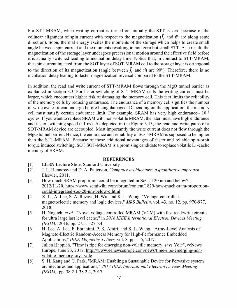
47
For STT-MRAM, when writing current is turned on, initially the STT is zero because of the colinear alignment of spin current with respect to the magnetization (𝐽𝐽𝑠𝑠 and 𝑚𝑚� are along same direction). Soon, thermal energy excites the moments of the storage which helps to create small angle between spin current and the moments resulting in non-zero but small STT. As a result, the magnetization of the storage layer undergoes precessional motion around the effective field before it is actually switched leading to incubation delay time. Notice that, in contrast to STT-MRAM, the spin current injected from the SOT layer of SOT-MRAM cell to the storage layer is orthogonal to the direction of its magnetization (angle between 𝐽𝐽𝑠𝑠 and 𝑚𝑚� are 90°). Therefore, there is no incubation delay leading to faster magnetization reversal compared to the STT-MRAM. In addition, the read and write current of STT-MRAM flows through the MgO tunnel barrier as explained in section 3.3. For faster switching of STT-MRAM cells the writing current must be larger, which encounters higher risk of damaging the memory cell. This fact limits the reliability of the memory cells by reducing endurance. The endurance of a memory cell signifies the number of write cycles it can undergo before being damaged. Depending on the application, the memory cell must satisfy certain endurance limit. For example, SRAM has very high endurance~ 1015 cycles. If you want to replace SRAM with non-volatile MRAM, the later must have high endurance and faster switching speed (~1 ns). As depicted in the Figure 3.13, the read and write paths of a SOT-MRAM device are decoupled. Most importantly the write current does not flow through the MgO tunnel barrier. Hence, the endurance and reliability of SOT-MRAM is supposed to be higher than the STT-MRAM. Because of these additional advantages of faster and reliable spin-orbit torque induced switching, SOT SOT-MRAM is a promising candidate to replace volatile L1-cache memory of SRAM.
REFERENCES [1] EE309 Lecture Slide, Stanford University [2] J. L. Hennessy and D. A. Patterson, Computer architecture: a quantitative approach.
Elsevier, 2011. [3] How much SRAM proportion could be integrated in SoC at 20 nm and below?
2012/11/20, https://www.semiwiki.com/forum/content/1829-how-much-sram-proportion-could-integrated-soc-20-nm-below-q.html
[4] X. Li, A. Lee, S. A. Razavi, H. Wu, and K. L. Wang, "Voltage-controlled magnetoelectric memory and logic devices," MRS Bulletin, vol. 43, no. 12, pp. 970-977, 2018.
[5] H. Noguchi et al., "Novel voltage controlled MRAM (VCM) with fast read/write circuits for ultra large last level cache," in 2016 IEEE International Electron Devices Meeting (IEDM), 2016, pp. 27.5.1-27.5.4.
[6] H. Lee, A. Lee, F. Ebrahimi, P. K. Amiri, and K. L. Wang, "Array-Level Analysis of Magneto-Electric Random-Access Memory for High-Performance Embedded Applications," IEEE Magnetics Letters, vol. 8, pp. 1-5, 2017.
[7] Julien Happich, "Time is ripe for emerging non-volatile memory, says Yole", eeNews Europe, June 23, 2017. http://www.eenewseurope.com/news/time-ripe-emerging-non-volatile-memory-says-yole
[8] S. H. Kang and C. Park, "MRAM: Enabling a Sustainable Device for Pervasive system architectures and applications," 2017 IEEE International Electron Devices Meeting (IEDM), pp. 38.2.1-38.2.4, 2017.

48
[9] S. W. Chung et al., "4Gbit density STT-MRAM using perpendicular MTJ realized with compact cell structure," in 2016 IEEE International Electron Devices Meeting (IEDM), 2016, pp. 27.1.1-27.1.4.
[10] K. Rho et al., "23.5 A 4Gb LPDDR2 STT-MRAM with compact 9F2 1T1MTJ cell and hierarchical bitline architecture," in 2017 IEEE International Solid-State Circuits Conference (ISSCC), 2017, pp. 396-397.
[11] C. Grezes, X. Li, K. Wong, F. Ebrahimi, P. Khalili Amiri, and K. L. Wang, "Voltage-controlled magnetic tunnel junctions with synthetic ferromagnet free layer sandwiched by asymmetric double MgO barriers," Journal of Physics D: Applied Physics, 2019/09/26 2019.
[12] W. J. Gallagher and S. S. P. Parkin, "Development of the magnetic tunnel junction MRAM at IBM: From first junctions to a 16-Mb MRAM demonstrator chip," IBM Journal of Research and Development, vol. 50, no. 1, pp. 5-23, 2006.
[13] X. Li, "Interface Engineering of Voltage-Controlled Embedded Magnetic Random Access Memory," PhD Thesis, University of California, Los Angeles, vol. Electrical and Computer Engineering, 2018.
[14] M. Durlam et al., "A 0.18 /spl mu/m 4Mb toggling MRAM," in IEEE International Electron Devices Meeting 2003, 2003, pp. 34.6.1-34.6.3.
[15] D. C. Worledge, "Single-domain model for toggle MRAM," IBM Journal of Research and Development, vol. 50, no. 1, pp. 69-79, 2006.
[16] S. Peng, "Rule deck compasion doesn't have to be difficult," Semiconductor Engineering, Jan 22 2015, Available: https://semiengineering.com/challenges-in-making-and-testing-mram/
[17] M. Imani, A. Rahimi, and T. Simunic, "A low-power hybrid magnetic cache architecture exploiting narrow-width values,” 2016 5th Non-Volatile Memory Systems and Applications Symposium, 2016, 10.1109/NVMSA.2016.7547174C.
[18] A. Fert, J.-M. George, H. Jaffrès, R. Mattana, and P. Seneor, "The new era of spintronics," Europhysics News, 2003, vol. 34 no. 6.
[19] K. Asifuzzaman, R. Sánchez Verdejo, P. Radojković, "Enabling a reliable STT-MRAM main memory simulation", In Proceedings of the International Symposium on Memory Systems (MEMSYS), October, 2017, Washington, DC, USA. Available: http://www.petarradojkovic.com/publications/MEMSYS-2017_Asifuzzaman.pdf
s[20] A. Fert, J-M. George, H. Jaffrès, R. Mattana, and P. Seneor, "The new era of spintronics", Europhysics News, vol. 34, no. 6, pp. 227-229, 2003. DOI: 10.1051/epn:2003609

49
Chapter 4: Beyond Conventional Spintronics
Xiang (Shaun) Li1, Sayeef Salahuddin2, and Shehrin Sayed2
1Department of Materials Science and Engineering, and Department of Electrical Engineering Stanford University
2Department of Electrical Engineering and Computer Sciences
University of California, Berkeley
4.0 INTRODUCTION Ferromagnetic materials are the key building blocks for spintronics due to its unique memory in the form of a long-range magnetization ordering. The magnetization can be switched with a magnetic field or a spin current induced torques (spin transfer or spin orbit torques). However, the large switching current in the existing magnetic memory devices is limiting the technological advancements in terms of the energy efficiency and the bit density. A possible route to address this technological limitation is to use a voltage or an electric-field based magnetization switching mechanism. There are many on-going parallel efforts to explore new materials and phenomena to enable such electric-field driven magnetization switching. In this chapter, we are going to discuss multiferroics materials and voltage controlled magnetic anisotropy, which are of great current interest to enable voltage controlled MRAM. 4.1 MULTIFERROICS Ferroic materials exhibit a long-range order in terms of a macroscopic property, and the order can be switched with an external field. Ferromagnets (FM) discussed in this book are a type of ferroic material, where the order arises from the spontaneous magnetization that can be switched with an external magnetic field. Other types of ferroic materials are ferroelectric (FE) and ferroelastic, which exhibit long-range ordering in terms of electric polarization and strain, respectively. The polarization of ferroelectric material can be switched with an electric-field, and the strain of the ferroelastic material can be switched with a uniaxial stress. Multiferroic refers to a material phase where more than one ferroic order coexists. In this book chapter, we restrict our discussion only in the material phase where both the ferromagnetic and the ferroelectric ordering coexists. Such materials are interesting for non-volatile memory like applications. A decoupled FM and FE orders imply the coexistence of a magnetic bit with an electric bit, giving rise to a four-state memory. However, if there is a coupling between the FM and the FE orders, it will allow us to switch the magnetic state just by switching the electric polarization using an electric field.

50
Figure 4.1. Ferroic materials and corresponding long-range ordering and switching fields.
4.1.1 FERROELECTRIC MATERIALS Before going into the details of the multiferroic materials, let us briefly discuss the ferroelectricity and their basic similarities with the ferromagnetism.
• Ferroelectric (FE) materials exhibit two polarization states, like the two magnetization states in ferromagnetic (FM) materials.
• The two polarization states are separated by an energy barrier as shown in Figure 4.2, like the anisotropy energy barrier in FM. The energy landscape of FE material is given by
𝑈𝑈 = 𝛼𝛼𝑃𝑃2 + 𝛽𝛽𝑃𝑃4 + 𝛾𝛾𝑃𝑃6 − 𝐸𝐸�⃗ ∙ 𝑃𝑃�⃗ Equation 4.1
where 𝑃𝑃�⃗ is the electric polarization vector with 𝑃𝑃 = �𝑃𝑃�⃗ � being its magnitude, 𝛼𝛼, 𝛽𝛽, and 𝛾𝛾 are the FE material constants. For BaTiO3, typical values of 𝛼𝛼, 𝛽𝛽, and 𝛾𝛾 are –1×10⁷ m-J/C2, –8.9×10⁸ m5-J/C4, and +4.5×10¹⁰ m9-J/C6, respectively.
• The FE polarization can be switched with an electric field, 𝐸𝐸�⃗ and the polarization direction (up or down) can be set by the polarity of the electric field. The time (𝑡𝑡) dependent switching dynamics is governed by the Landau-Khalatnikov (LK) equation, given by
𝜌𝜌 𝑑𝑑𝑑𝑑𝑑𝑑𝑑𝑑
+ ∇𝑑𝑑𝑈𝑈 = 0 Equation 4.2
where 𝑈𝑈 is given by Equation 4.1, 𝑃𝑃 is the magnitude of the electric polarization, and 𝜌𝜌 is an internal resistivity of the ferroelectric material. Here ∇𝑑𝑑= 𝑥𝑥� 𝜕𝜕
𝜕𝜕𝑚𝑚+ 𝑦𝑦� 𝜕𝜕
𝜕𝜕𝜕𝜕+ �̂�𝑧 𝜕𝜕
𝜕𝜕𝑧𝑧. Similar to
the M-H hysteresis loop observed in FM materials, we observe a P-E hysteresis loop in FE materials (Figure 4.1).
• Ferroelectricity is demonstrated below a certain phase transition temperature, called the Curie temperature, similar to that observed in ferromagnetism.

51
Figure 4.2. Energy landscape of a ferroelectric material without an external electric field.
Most ferroelectric materials are transition metal oxides. The positively charged transition metal ions (cations) have empty d-shells, which forms molecules with neighboring negative oxygen ions (anions). A collective shift of cations and anions inside a periodic crystal induces the net electric polarization. For example, see the ABO3 perovskite structure in Figure 4.3 which corresponds to the ferroelectric material BaTiO3. The unit cell of BaTiO3 comprises a Ti4+ cation (B-site) caged within a corner-linked network of O2- octahedra. The Ba2+ ions are situated on the A-sites. The polarization occurs due to a shift of the Ti4+ ion with respect to the O2- ions. The electronic configuration of a Ti atom is given by
Ti: [Ar] 3d2 4s2
where [Ar] represents the electronic configuration of noble gas argon1. It can be noted that the key element of the ferroelectricity, the Ti4+ ion corresponds to an empty d-shell as mentioned earlier. However, magnetism requires transition metal ions with partially filled d-shells and exchange interaction between the uncompensated spins of the ions give rise to a long-range magnetic order (see earlier chapters for details). Thus, these two conventional d-shell based mechanisms for ferroelectricity and ferromagnetism can not coexist in conventional FE and FM materials. Moreover, ferroelectric materials are usually insulating. Because if it was conducting like metals, the mobile electrons would have screened out the electric polarization. On the other hand, most materials with strong ferromagnetic order are metallic, although we can observe an anti-ferromagnetic order in various insulating materials.
1 1 Ar: 1s22s22p63s23p6

52
Figure 4.3. ABO3 perovskite structure of a ferroelectric e.g. BaTiO3.
4.1.2 COEXISTENCE OF THE FERROELECTRICITY AND THE FERROMAGNETISM The conventional d-shell based mechanisms for FE and FM are mutually exclusive, as explained above. In order to achieve both FE and FM ordering within the same material, either (i) a non-empty-d-shell based mechanism for the ferroelectricity or (ii) a non d-electron based mechanism for magnetism is required. The former strategy has been achieved in various material systems, where anti/ferromagnetism arises due to the partially filled d-shell in the transition metal ion, but the ferroelectricity arises due to a different origin (see Figure 4.4) as summarized below.
• The widely explored multiferroic material of ABO3 structure (see Figure 4.4a), BiFeO3 have a FE order due to the Bi3+ cations on the A-sites. but the long-range antiferromagnetic (AFM) order arises due to the 3d electrons in Fe cations on the B-site. Note that the electron configuration of Bi atom is given by
Bi: [Xe] 4f14 5d10 6s2 6p3
where [Xe] is the electronic configuration of the noble gas xenon2. The Bi3+ cation has a pair of electrons in the 6s orbital which do not go through sp hybridization and creates a local dipole with spontaneous polarization of ~100 μC/cm2. The FE ordering occurs below the Curie temperature of 1103 K and the AFM ordering occurs below the Néel temperature of 643 K, which makes BiFeO3 a room temperature multiferroic material.
• The ferroelectricity also arises due to a geometrical ionic shift due to the structural instabilities (see Figure 4.4b), as typically observed in hexagonal RMnO3 (R = Sc, Y, In,
2 Xe: 1s2 2s2 2p6 3s2 3p6 3d10 4s2 4p6 4d10 5s2 5p6

53
or Dy-Lu), hexagonal LuFeO3, and BaNiF4 (due to an asymmetry between Ba2+ and F- ions).
Figure 4.4. Various non-empty-d-shell based mechanisms for ferroelectricity in multiferroic materials. Ferroelectricity occurs due to (a) bond chemistry of a pair of valence electron in 6s orbital of Bi3+ ion in BiFeO3, (b) a geometrical instability induced ionic shift, and (c) charge ordering [A]. Another mechanism of ferroelectricity has been observed in LuFe2O4 due to the charge ordering of the alternating sequence of Fe2+ and Fe3+ ions (see Figure 4.4c).
The latter strategy has been observed in EuTiO3 or (Ba,Eu)TiO3 alloys, where the ferroelectricity arises from the conventional empty-d-shells in Ti cations. The magnetic order arises from the f-electrons in Eu2+. The electron configuration of Eu is given by
Eu: [Xe] 4f7 6s2
There are many on-going efforts to explore various independent mechanisms to achieve both of these ferroic ordering within the same phase of materials. Interested readers can study the review papers mentioned in Section 4.1.4 for further reading.

54
4.1.3 APPLICATION IN NON-VOLATILE MEMORY The room temperature multiferroic perovskite like BiFeO3 is promising to enable electric field controlled non-volatile magnetic memory. As mentioned above, the material exhibits a ferroelectric order due to the Bi ions and an antiferromagnetic order due to the Fe ions. The coupling between the ferroelectricity and the antiferromagnetism offers a non-volatile control on the antiferromagnetic axis with an external electric field. It has been discussed that in BiFeO3, as well as in many other multiferroics, a weak ferromagnetic moment arises due to the canting of the antiferromagnetically aligned Fe3+ spins caused by the Dzyaloshinskii-Moryia interaction. Although such weak ferromagnetic moment may not be interesting for memory applications by itself, but it is possible to couple it to an adjacent ferromagnetic layer through exchange coupling and switch the magnetic bit in the FM material by applying an electric field on the BiFeO3.
Figure 4.5. Electric-field controlled device with multiferroics
4.1.4 FURTHER READING ON MULTIFERROICS 1. M. Fiebig, T. Lottermoser, D. Meier, and M. Trassin, “The evolution of multiferroics”,
Nature Reviews Materials, 1, 16046, 2016. 2. R. Ramesh and N. A. Spaldin, “Multiferroics: progress and prospects in thin films”, Nature
Materials, 6, 21-29, 2007. 3. N. A. Spaldin and R. Ramesh, “Advances in magnetoelectric multiferroics”, Nature
Materials, 18, 203-212, 2019. 4. S.-W. Cheong and M. Mostovoy, “Multiferroics: a magnetic twist for ferroelectricity”,
Nature Materials, 6, 13-20, 2007. 5. C. Binek and B. Doudin, “Magnetoelectronics with magnetoelectrics”, Journal of Physics:
Condensed Matter, 17, L39–L44, 2005. 6. L. W. Martin “Engineering functionality in the multiferroic BiFeO3–controlling chemistry
to enable advanced applications”, Dalton Trans., 39, 10813–10826, 2010.

55
4.2 VOLTAGE-CONTROLLED MRAM The writing mechanisms of Oersted field, STT, and SOT mentioned in the last Chapter all utilize current-controlled means [2], [3] to write information into magnetic bits. However, the use of currents results in a memory cell size (i.e. bit density) limitation due to the large size of the required access transistors [4] and large dynamic switching energy due to Ohmic power dissipation. Another promising method to reduce the power consumption of MRAM is to use voltage instead of current to switch the magnetic free layer. In recent years, writing of information using the electric field in perpendicular magnetic tunnel junctions (MTJs) [5], [6], is being investigated intensively, with the goal of realizing energy-efficient and high-density voltage-controlled (VC) MRAM devices [7].
Figure 4.6. (a) Schematic of magnetoresistance curves of a perpendicular MTJ under an out-of-plane magnetic field, measured when different voltage is applied. (b) Schematic showing the process of magnetization switching using the VCMA effect. If the applied voltage is large enough to eliminate the energy barrier, under an in-plane bias magnetic field, precessional motion can happen. (c) Free layer magnetization 𝑚𝑚��⃗ precession trajectory during the VCMA pulse. 𝑑𝑑��⃗ 𝑒𝑒𝑒𝑒𝑒𝑒 refers to total effective magnetic field which mainly consists of the built-in or applied in-plane bias magnetic field. The magnetization direction can be controlled by precisely timing of the voltage pulse duration. The time difference between 𝑡𝑡1 and 𝑡𝑡2 is half of the free layer precession period. (d) Schematic of voltage-controlled MTJ resting on a metal electrode with high SOC, which can generate SOT onto the MTJ when a current is passed through [8].

56
Essentially, instead of using spin-polarized current, the charge accumulation and depletion at the tunnel barrier surface will modulate the magnetic anisotropy, which can drastically reduce the energy barrier for free layer reversal. The electric-field effect, or the voltage-controlled magnetic anisotropy (VCMA) effect, is utilized to temporarily lower the interfacial perpendicular magnetic anisotropy (PMA) of the free layer during the writing operation, thus reducing the writing energy required to overcome the energy barrier between the two stable magnetization states, as shown in Figure 4.6(a-b). In order to enhance the effect of VCMA and suppress the effect of STT, a thicker MgO barrier is usually used, resulting in a much smaller write and read current, thus lower power consumption. There are several different ways of utilizing this VCMA effect to switch the free layer. Because the VCMA effect temporarily lowers the energy barrier, any other switching mechanisms can be combined with the VCMA effect to reduce the energy consumption of that switching mechanism. Examples include Oersted field generated from a write wire, spin transfer torque [9], or spin orbit torques [10]. Thermal activation can also help achieve the switching when the energy barrier is sufficiently low. If the energy barrier is fully eliminated by the VCMA effect and there is an in-plane bias field built into the MTJ stack, the free layer will start precessional motion and oscillate between up and down directions until damping forces the free layer magnetization to align to the in-plane bias layer orientation, as shown in Figure 4.6(c) and Figure 4.7. In this precession process, removing the applied voltage pulse will recover the energy barrier and the magnetization will choose to stay at the closest local minima. Hence, a precise timing of the voltage pulse to be half of the precession period is essential to enable high switching probability and low write error rate (WER).
Figure 4.7. (Left) Experimental results of voltage controlled switching probability as a function of the voltage pulse width. (Right) Schematic of the voltage-induced precessional switching of MTJ free layer [11].

57
In order to achieve a low WER, good timing and pulse shape are required by the writing circuitry. It is also possible to utilize multiple read/write cycles to lower the total WER [12]. However, there are couple of device-level parameters that are critical in decreasing the WER, including damping factor, thermal stability, and external in-plane field strength. In addition to the write operation, the read operation of a memory device is also critical. VC-MRAM inherently has a thicker MgO tunnel barrier than the STT-MRAM, which will give rise to higher resistance-capacitance delay in the sensing circuit. However, there are some other factors that might remedy this high resistance-induced low read speed. First, as the MgO barrier in a VC-MRAM device is usually around 1.4 nm [13] compared with that of around 0.9 nm [14] for a STT-MRAM device, the TMR values will increase giving rise to a larger read margin. The cause of this is usually attributed to the better crystal quality of the barrier and/or the less shorting of the sidewall when the barrier is thicker. Secondly, as STT-MRAM uses positive and negative polarities to induce switching from anti-parallel to parallel and vice versa, if read current is large and close to the write current level, the read operation can induce switching of the memory bit, or the so-called read disturbance. Therefore, the read voltage needs to be relatively small to around 0.3-0.4V to avoid large read disturbance. While for VC-MRAM, only the positive polarity is used when writing. Hence one can use the negative polarity VDD value of around -1V for reading to achieve larger read margin as shown in Figure 4.8. In addition, due to the linear VCMA effect, the negative voltage applied to a VC-MRAM device can increase the thermal stability thus further reduce the read disturbance [12].
Figure 4.8. (Top) Schematic of STT-MRAM and MeRAM read voltage range with respect to the write voltage. (Bottom) Thermal stability and measured (circles) and simulated (squares) read disturbance rate as a function of sensing voltage for read pulses of 1, 10, 100, and 1000 ms for a MeRAM device [12].

58
Apart from embedded memory replacement, VC-MRAM cells can be utilized for a variety of logic circuits. One example is look-up tables (LUT), which are the core components in programmable logic circuits. By resting the voltage-controlled MTJ upon a spin-orbit torque (SOT) bus as shown in Figure 4.6(d), the VCMA pulse selects the device to program by lowering the energy barrier, while the SOT bus exerts spin torque onto the selected MTJ. This enables deterministic switching and parallel programming, where all bits that have the same to-be-written data can be written simultaneously [15]. Voltage-controlled MRAM cells can also serve as building blocks for novel computing paradigms. For example, stochastic computing processes information in the form of probabilities, represented in binary streams and has the advantages of parallelization, error resiliency, and area efficiency, making it beneficial for applications such as artificial intelligence (learning and recognition) and informatics (sensor and social networks). A main challenge in stochastic computing is the generation of the true-random bit stream with different probabilities. With the VCMA-on-SOT structure shown in Figure 4.6(d), as VCMA drives the MTJ into a meta-stable state, current flowing through the SOT material simultaneously injects spin torque into the MTJ, biasing the switching probability proportional to the amplitude and polarity of the current [16]. The integrated VC-MRAM structure with SOT assisted-writing has also been proposed to implement in-memory computing, where logic operations can be applied on the MTJ state without an intermediate readout of the device [17], [18].
REFERENCES [1] M. Fiebig, et al, "The evolution of multiferroics," Nature Reviews Materials, vol. 1,
2016, https://doi.org/10.1038/natrevmats.2016.46. [2] I. M. Miron et al., "Perpendicular switching of a single ferromagnetic layer induced by
in-plane current injection," Nature, vol. 476, no. 7359, pp. 189-93, Aug 11 2011. [3] L. Liu, O. J. Lee, T. J. Gudmundsen, D. C. Ralph, and R. A. Buhrman, "Current-Induced
Switching of Perpendicularly Magnetized Magnetic Layers Using Spin Torque from the Spin Hall Effect," Physical Review Letters, vol. 109, no. 9, p. 096602, 08/29/ 2012.
[4] P. Khalili and K. L. Wang, "The Computer Chip That Never Forgets," (in English), Ieee Spectrum, vol. 52, no. 7, pp. 30-35, Jul 2015.
[5] W. G. Wang, M. Li, S. Hageman, and C. L. Chien, "Electric-field-assisted switching in magnetic tunnel junctions," Nat Mater, vol. 11, no. 1, pp. 64-8, Jan 2012.
[6] Y. Shiota, T. Nozaki, F. Bonell, S. Murakami, T. Shinjo, and Y. Suzuki, "Induction of coherent magnetization switching in a few atomic layers of FeCo using voltage pulses," Nat Mater, vol. 11, no. 1, pp. 39-43, Jan 2012.
[7] P. Khalili Amiri et al., "Electric-Field-Controlled Magnetoelectric RAM: Progress, Challenges, and Scaling," Magnetics, IEEE Transactions on, vol. 51, no. 11, pp. 1-7, 2015.
[8] X. Li, A. Lee, S. A. Razavi, H. Wu, and K. L. Wang, "Voltage-controlled magnetoelectric memory and logic devices," MRS Bulletin, vol. 43, no. 12, pp. 970-977, 2018.

59
[9] S. Kanai et al., "Magnetization switching in a CoFeB/MgO magnetic tunnel junction by combining spin-transfer torque and electric field-effect," Applied Physics Letters, vol. 104, no. 21, p. 212406, 2014.
[10] L. Liu, C.-F. Pai, D. Ralph, and R. Buhrman, "Gate voltage modulation of spin-Hall-torque-driven magnetic switching," arXiv preprint arXiv:1209.0962, 2012.
[11] H. Noguchi et al., "Novel voltage controlled MRAM (VCM) with fast read/write circuits for ultra large last level cache," in 2016 IEEE International Electron Devices Meeting (IEDM), 2016, pp. 27.5.1-27.5.4.
[12] C. Grezes et al., "Write Error Rate and Read Disturbance in Electric-Field-Controlled Magnetic Random-Access Memory," IEEE Magnetics Letters, vol. 8, pp. 1-5, 2017.
[13] C. Grezes et al., "Ultra-low switching energy and scaling in electric-field-controlled nanoscale magnetic tunnel junctions with high resistance-area product," Applied Physics Letters, vol. 108, no. 1, p. 012403, 2016.
[14] K. Watanabe, B. Jinnai, S. Fukami, H. Sato, and H. Ohno, "Shape anisotropy revisited in single-digit nanometer magnetic tunnel junctions," Nature Communications, vol. 9, no. 1, p. 663, 2018/02/14 2018.
[15] H. Lee, F. Ebrahimi, P. K. Amiri, and K. L. Wang, "Low-Power, High-Density Spintronic Programmable Logic With Voltage-Gated Spin Hall Effect in Magnetic Tunnel Junctions," IEEE Magnetics Letters, vol. 7, pp. 1-5, 2016.
[16] H. Lee, A. Lee, F. Ebrahimi, P. K. Amiri, and K. L. Wang, "Analog to Stochastic Bit Stream Converter Utilizing Voltage-Assisted Spin Hall Effect," (in English), Ieee Electron Device Letters, vol. 38, no. 9, pp. 1343-1346, Sep 2017.
[17] H. Zhang, W. Kang, L. Z. Wang, K. L. Wang, and W. S. Zhao, "Stateful Reconfigurable Logic via a Single Voltage-Gated Spin Hall-Effect Driven Magnetic Tunnel Junction in a Spintronic Memory," (in English), Ieee Transactions on Electron Devices, vol. 64, no. 10, pp. 4295-4301, Oct 2017.
[18] S.-h. C. Baek et al., "Complementary logic operation based on electric-field controlled spin–orbit torques," Nature Electronics, vol. 1, no. 7, pp. 398-403, 2018/07/01 2018.