![Multi-objective Gain-Impedance Optimization of Yagi-Uda ... · better optimization technique for Yagi-Uda antenna designs, in [30]. In this paper, use of BBO, Blended BBO and NSPSO](https://static.fdocuments.net/doc/165x107/60b31a32028c620c9e76b00e/multi-objective-gain-impedance-optimization-of-yagi-uda-better-optimization.jpg)
The Yagi-Uda Antenna
25
The Yagi-Uda Antenna 12/15/2020 1 The Inventor-Uda
Transcript of The Yagi-Uda Antenna

The Yagi-Uda Antenna
12/15/2020 1
The Inventor-Uda

Presentation Agenda
Part 1• Introduction• Motivation• Description/Key Characteristics• Qualitative Theory of Operation• Conclusions
Part 2 (date TBD)
• Design Approaches• Yagi Impedance• Matching• Conclusions
Look For The bottom line
12/15/2020 2
Presenter-Tom KJ6PST

Introduction-The Yagi-Uda Antenna
• A Layman’s Curiosity For A Popular Ham Antenna
• Disclaimers
– I’m an electrical engineer, but
– I’m not an antenna engineer
• Don’t use a Yagi, wish I could (HOA would not approve)
• Have not analyzed or designed a Yagi
• Have searched on-line publications as the basis for this presentation
12/15/2020 3
I’m not an expert

“Tower of Yagi Arrays” on Preston Road
This arrays owner should be presenting!
12/15/2020 4
Yes, there are6 Yagi antennas

Introduction-A Few Yagi-Uda Antenna Uses
Commercial Antenna often used by utility companies
Commercial Ham Tri-bander
12/15/2020 5
The Yagi Antenna has found a number of applications
1950 rooftop TV antennaMilitary Search Radar

Some Commercial Ham Yagis
Cushcraft A3S Yagi HyGain TH3-MK3
• Electrical:– Gain (ave.) 5.8 dBd (8.0 dBi)
– Front-To-Back Ratio (max.) 25 dB
– Maximum Power 1500 Watts PEP
– VSWR at resonance Less than 1.5:1
– Input Impedance 50 ohms
– Matching System Beta (DC Ground)
• Mechanical:– Boom Length 14 ft. (4.3m)
– Boom Diameter 2 in. (51mm)
– Longest Element 27’ 5” (8.36m)
12/15/2020 6
Note key electrical characteristics: Directivity (Gain), F/B, SWR
dBi
2:1 SWR BW~ 3-4%

Units Specifying Yagi “Gain” and F/B• The dB = 10*log10 (P1/P2)
• If P1/P2=100, in dB , (P1/P2)dB =20 dB
• If (PF/PB)= 25dB, then (PF/PB)=316, a ratio of power densities
• The directive gain of an isotropic antenna is 0dBi (i for isotropic)
• The directive gain of a dipole antenna is ~2.15dBi=dBd
12/15/2020 7
Isotropic Antenna (theoretical)power density, Po/4pi is equal at
every point on the spherePo= antenna radiated power
Ideal Dipole AntennaPmax= 1.65 (Po/4pi)
dBd=10*log ((1.65 Po/4pi)/(Po/4pi))10log (1.65)=2.15dBi=dBd
Pmax
Po/4pi
An antenna’s directivity (gain) can be expressed in dBi or dBd
Isotropicpattern

Motivation
• MARC uses 20,15 &10 meter Yagis (mono-banders) for Field Day
• Yagi gain enhances opportunity for successful contacts
• Although widely used; operational principles sometimes
vaguely understood
12/15/2020 8
20 M Yagi Stacked 15 & 10 M Yagis
Presentation goal- to present basic Yagi operation and appreciate a remarkable antenna

Yagi Array Physical & Electrical Illustration
The Yagi construction is elegantly simple- one driven elementwith one or more parasitic elements. The Yagi operation is simply
complicated due to inter-element coupling
12/15/2020 9
Parasitic elements
The radiation patternis determined by allelement currents.

Yagi Key Characteristics
Primary
• Radiation Pattern
– Directive Gain
– Front-back Ratio
– Sidelobes
• SWR Bandwidth
Secondary (Part II Presentation)
• Input Impedance (Driving point impedance)
Designers select the pattern characteristic that is most
important to their operating requirements
12/15/2020 10

How Does The Yagi Work?
• The driven element (DE) current radiates an electric field
• That field induces currents on the passive (parasitic) elements (reflector and directors)- mutual coupling
• Those element currents in turn radiate fields
• All parasitic fields combine by phase adjustment with the DE field to create the radiation pattern with a beam (constructive and destructive interference)
The Yagi element fields add as vectors to produce the array’sgain, F/B ratio and sidelobes
12/15/2020 11

12/15/2020 12
Yagi Radiation Pattern Illustration
Back lobe Main lobe actslike a
“spatial filter”
Side lobes
What produces this pattern?-E-field Vector Addition
Desiredsignal
Interferingsignal
Interferingsignal
This pattern is the same for both Tx and Rx

12/15/2020 13
What’s A Vector And Vector Addition?
Vector addition includes both magnitude and direction (phase)
12/15/2020 13
Definition-A quantity with magnitude and direction. It can be represented by an arrow whose length indicates magnitude and whose tip represents direction
Roadmap Example Circuit Voltage Example
indicates phase lag of current i relative to V1
V1=V2+V3
V1
V2=R*i
V3=jXl*i
i
R
AssumeR=2, Xl=1V2=V1*(.8-j.4)V3=V1*(.2+j.4)
Map coordinates
X (re)
Y (j)
Vector Voltage coordinates
E (900)
N (00 or 3600)
W (2700)
S (1800)
~270
V1
V3V2
Y
X (use as reference)A
B
C
V1=2E
V2=.5E+1N
V1+V2= V3=2.5E+1N
~630
N
E
d~700
What’s About E-field Vector Addition?
E fields add as vectors
12/15/2020 14
The phase, , indicates that the vector magnitudes do not occur simultaneously
just as we observed with the circuit voltages
E-field Example
E1
E2
Here phase indicates relative direction or phase rotation between E1 and E2
E3=E1+E2
|E3|=[E12+E22+2E1E2cos ].5
X (re)
Y (j) See Casler,Vectors/phasors
Nov. 2020 QSTPage 34-37,
12/15/2020 15
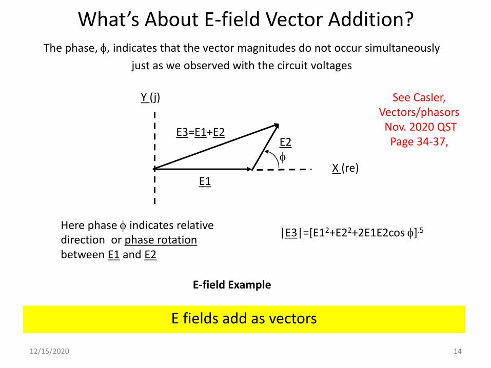
E1= 1*sin(2pi*f*x/c)
E2= 0.5*sin(2pi*f*x/c+ phi=0)
E1+E2, phi=0, Et=1.5
E1+E2, phi=90deg, Et=1.1
E1+E2, phi=180deg, Et=0.5
0deg 90deg 180deg
E2= 0.5*sin(2pi*f*x/c+ phi=90)
360deg
X
Phase angle indicates vector peak amplitude relationship
reference
In phase
900
shift
constructive
constructive
destructive
12/15/2020 16
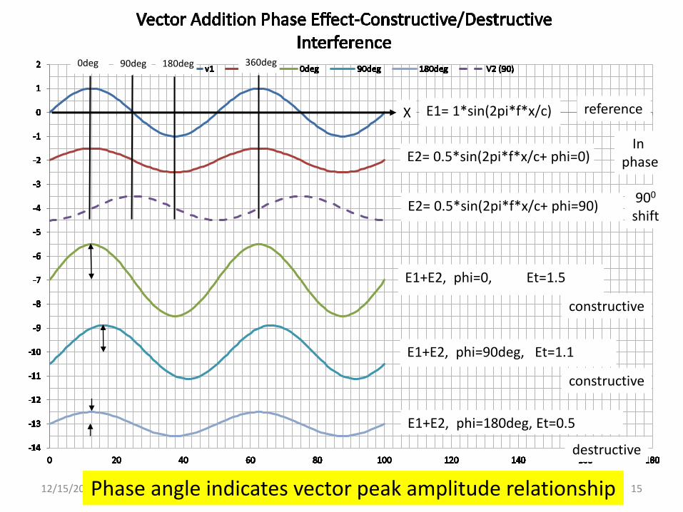
How Is A Beam Formed? 2-Driven Elements Example
A “beam’ is formed by constructive interference Its all in the phase
E1= 1 00
E2=1 -900
d= 900, pi/2
Propagation direction
Total E field=0 Destructive interference
Total E field=2 Constructive interference= a beam (yes, broad in this example)
Propagation direction
0
0.5
1
1.5
2
1
1
2
null
A B
C
D
A B
C
D

The Radiation Fields, Eq &H Of A Current Element
The electric field is proportional to element current amplitude and phase
12/15/2020 17
Eq= Iz * G(r, , q)Eq is directly proportional tothe magnitude and phase of Iz.G(r, , q) describes the radiationspatial pattern
Iz
Single element pattern
Where Iz=|Iz|ang(y), y= phase

The 1st of Two Critical Phases For Yagi Design
Phase 1 is the first design parameter to choose and vary
12/15/2020 18
V1
Port 1
Port 2 Short circuit
Driven elementL1~ l/2
Element Spacing=d11=2pd1/l
E1E1’=E1(-j1)
V2+V2’ =0
V2= Port 2 induced voltage By E1’, but Port2 is short circuitedthus there is a V2’ such thatV2+V2’=0, or V2’=-V2~-1
Port 2
Spacing=d1
Parasitic element

The 2nd Critical Phase, 2, Varies With Element Length
The designer iteratively varies 1 and 2 to achieve the best compromise between gain, F/B ratio and sidelobes
12/15/2020 19
Director length, L2L2< l/2 Port Z22=R+jXc, length dependent
2=atan (Xc/R)V2+V2’ =0
I2
I2
Port 2
E2
I2 is produced by V2’I2=V2’/Z22=-V1’/Z22i2 ~1+2
E2 is produced by i2Therefore, E2~1+2
inductive
capacitive

3 Element Array Mutual Coupling Illustration
All mutual coupling must be included to determine the array element currents
12/15/2020 20
V1 V2=0 V3=0I1 I2sc I3sc
Port 1 Port 2 Port 3
Driven element 2nd director1st director
primary
primary secondary
primary
secondary
secondary

Thiele’s Mutual Coupling Analysis Determined All Parasitic Element Current Amplitudes and Phases
12/15/2020 21
The DE current amplitude is the largest, the director current amplitudes are approximately equal. All the currents produce E
fields resulting in the radiation pattern (vector addition)
DE
Director spacing =0.33 l

The Maximum Radiated E Field Is Limited By Each Director’s Phase, Vector Addition
Note: Because each director’s E field has a different phase, the array’s max E field is less than the ideal (all in phase)!
12/15/2020 22
Ld=0.415l
Pattern Total E field
ThenIdeal maximum E field magnitude
DE D1 D3 D5D4D2 D6
Ideal : If all fields in phase
Vector addition of array element fields

Element Field Vector Phases Produce The F/B Ratio Example
The element electric field vector phases are key to make Ef>Eb
12/15/2020 23
Reflector
Driven Element
Director
Eb=Er+Ede+Edir Ef=Er+Ede+Edir
F/B ~ |Ef|2/|Eb|2
Ede
Er
EdirEf
Ede
ErEdirEb
destructiveconstructive

Conclusions-Part 1
• The Yagi Array:
– Provides gain with 1 driven element and several parasitic elements
– Relies on judicious element-element spacing and element length-directly affects E-field phase
– Pattern is a result of E-field vector addition
– Has a “beam” radiation pattern that provides spatial filtering;
– Is relatively simple to construct- only 1 driven element
• The Yagi performance:
– Is based on complex inter-element coupling
– Depends upon element length and inter-element spacing
– Depends on the choices of the critical phases (1 & 2)
12/15/2020 24
Bottom line : It is a winner

References1. Wikipedia, “Yagi-Uda Antenna”
2. Thiele, Gary A., Analysis of Yagi-Uda Type Antennas” IEEE Trans. On antennas & Propagation, Vol. AP-17, No.1, Jan., 1969
3. “Yagi Antenna/ Yagi-Uda Aerial”
4. Viezbricke, Peter, “Yagi Antenna Design”, Nat. Bur. Standards TN688, December, 1976
5. Ch25, “Coupled Antennas “ , http://eceweb1.rutgers.edu/~orfanidi/ewa/ch25.pdf
6. Steyer, Martin, DK7ZB, “ 3 Element-Yagi, 20m/15m/10m, 28Ohm Design”, www.qsl.net/dk7zb
7. Magliacane, John, KD2BD, “Thoughts on Perfect Impedance Matching of a Yagi”
8. Wortman, Bill, N6MW, “ The Hairpin Match”
9. vu2nsb.com/antenna/yagi-antennas/
10. ARRL Antenna Handbook
11. Casler, “Exploring Radio Math.”, QST, Nov.,20, pgs 34-37
12/15/2020 25