The UNIVERSITY of NORTH CAROLINA at CHAPEL HILL RAM Basics Anselmo Lastra.
56
The UNIVERSITY of NORTH CAROLINA at CHAPEL HILL RAM Basics Anselmo Lastra
-
Upload
jason-dorsey -
Category
Documents
-
view
216 -
download
2
Transcript of The UNIVERSITY of NORTH CAROLINA at CHAPEL HILL RAM Basics Anselmo Lastra.

The UNIVERSITY of NORTH CAROLINA at CHAPEL HILL
RAM Basics
Anselmo Lastra

The UNIVERSITY of NORTH CAROLINA at CHAPEL HILL
Topics
VGA timing projectDeadline Thursday
Class time changeSemester project topicsRAMs

The UNIVERSITY of NORTH CAROLINA at CHAPEL HILL
Class Time
Preference for keeping TThUnfortunately, no open time for all

The UNIVERSITY of NORTH CAROLINA at CHAPEL HILL
Projects
Some have project alreadyPolygon pipeline
Stopping points: Gouraud, texturing, etc.
Ray caster/tracerSimilar possible milestones
Can share common parts

The UNIVERSITY of NORTH CAROLINA at CHAPEL HILL
Simple Hdw View of RAM
Some capacity 2k
k bits of address linesOften multiplexed
Maybe have read line, clock, chip selectHave a write enable line

The UNIVERSITY of NORTH CAROLINA at CHAPEL HILL
Reading
Setup address linesActivate enable, read/write lineData available after specified amt of time

The UNIVERSITY of NORTH CAROLINA at CHAPEL HILL
WritingSetup address linesSetup data linesActivate write line

The UNIVERSITY of NORTH CAROLINA at CHAPEL HILL
Static vs Dynamic RAM
SRAM vs DRAMDRAM stores charge in what’s essentially capacitor
Disappears over short period of timeMust be refreshed (rewritten/recharged)
SRAM easier to useFasterMore expensive per bitSmaller sizes

The UNIVERSITY of NORTH CAROLINA at CHAPEL HILL
Structure of SRAM
Control logicOne memory cell per bit
Cell consists of one or more transistorsNot really a latch made of logic
Logic equivalent

The UNIVERSITY of NORTH CAROLINA at CHAPEL HILL
Bit Slice
Cells connected to form 1 bit positionWord Select gates one latch from address linesNote it selects Reads alsoB (and B not) set by R/W, Data In and BitSelectFunny thing here when you write. What is it?

The UNIVERSITY of NORTH CAROLINA at CHAPEL HILL
Bit Slice can Become Module
Basically bit slice is a X1 memoryNext

The UNIVERSITY of NORTH CAROLINA at CHAPEL HILL
16 X 1 RAM
Now shows decoder
The UNIVERSITY of NORTH CAROLINA at CHAPEL HILL
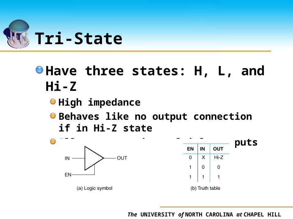
Tri-State
Have three states: H, L, and Hi-Z
High impedanceBehaves like no output connection if in Hi-Z stateAllows connecting multiple outputs

The UNIVERSITY of NORTH CAROLINA at CHAPEL HILL
Multiplexed with Hi-Z
Normal behavior is blue area

The UNIVERSITY of NORTH CAROLINA at CHAPEL HILL
Row/Column
If RAM gets large, there is a large decoderAlso run into chip layout issuesLarger memories usually “2D” in a matrix layoutNext Slide

The UNIVERSITY of NORTH CAROLINA at CHAPEL HILL
16 X 1 as 4 X 4 Array
Two decoders
RowColumn
Address just broken upNot visible from outside

The UNIVERSITY of NORTH CAROLINA at CHAPEL HILL
Change to 4 X 2 RAM
Minor change in logicAlso pinouts

The UNIVERSITY of NORTH CAROLINA at CHAPEL HILL
Realistic Sizes
Imagine 256K memory as 32K X 8One column layout would need 15-bit decoder with 32K outputs!Can make a square layout with 9-bit row and 6-bit column decoders

The UNIVERSITY of NORTH CAROLINA at CHAPEL HILL
SRAM Performance
Current ones have cycle times in low nanoseconds (say 2.5ns)Used as cache (typically offchip secondary cache)Sizes up to 8Mbit or so for fast chips

The UNIVERSITY of NORTH CAROLINA at CHAPEL HILL
Using SRAM on Spartan II
Recall block SRAM available on chip11 4Kb blocksConfigured in many ways (table)

The UNIVERSITY of NORTH CAROLINA at CHAPEL HILL
Using from Verilog
Instantiate a block (here called R1)
RAMB4_S8_S8 R1 (.DOA (data_a), .DOB (data_b), .ADDRA (addr_a), .ADDRB (addr_a), .CLKA (clk), .CLKB (clk), .DIA (data_in), .DIB (data_in), .ENA (ena), .ENB (enb), .RSTA (rsta), .RSTB (rstb), .WEA (wea), .WEB (web));

The UNIVERSITY of NORTH CAROLINA at CHAPEL HILL
Can Initialize
Have to do it two ways, one for simulator, another for hardware
//synthesis attribute INIT_00 of R1 is "08192A3B4C5... total of 256 bits (64 hex characters)..."
//synthesis attribute INIT_01 of R1 is "08192A3B4C5D6E7F08192A3B4C5D6E7F08192A3B4C5D6E7F08192A3B4C5D6E7F“
// Up to INIT_0F
Above is for hardware (next software)

The UNIVERSITY of NORTH CAROLINA at CHAPEL HILL
For Simulation
//synopsys translate_off
defparam R1.INIT_00 = 64'h08192A3B4C5D6E7F08192A3B4C5D6E7F08192A3B4C5D6E7F08192A3B4C5D6E7F; // 256-bit hex value
defparam R1.INIT_01 = 64'h08192A3B4C5D6E7F08192A3B4C5D6E7F08192A3B4C5D6E7F08192A3B4C5D6E7F; // 256-bit hex value
... defparam R1.INIT_0F = 64'h08192A3B4C5D6E7F08192A3B4C5D6E7F08192A3B4C5D6E7F08192A3B4C5D6E7F; // up to INIT_0F
//synopsys translate_on

The UNIVERSITY of NORTH CAROLINA at CHAPEL HILL
Look at Test Code
My RAM loading example from undergrad class
http://www.cs.unc.edu/~lastra/comp190/Assignments/block_ram_C.txt

The UNIVERSITY of NORTH CAROLINA at CHAPEL HILL
Dynamic RAM
Capacitor can hold chargeTransistor acts as gateNo charge is a 0Can add charge to store a 1Then open switch (disconnect)Can read by closing switch
Explanation next

The UNIVERSITY of NORTH CAROLINA at CHAPEL HILL
Precharge and Sense AmpsYou’ll see “precharge time”B is precharged to ½ VCharge/no-charge on C will increase or decrease voltageSense amps detect this

The UNIVERSITY of NORTH CAROLINA at CHAPEL HILL
DRAM Characteristics
Destructive ReadWhen cell read, charge removedMust be restored after a read
RefreshAlso, there’s steady leakageCharge must be restored periodically

The UNIVERSITY of NORTH CAROLINA at CHAPEL HILL
DRAM Logical Diagram

The UNIVERSITY of NORTH CAROLINA at CHAPEL HILL
DRAM Read Signaling
Lower pin count by using same pins for row and column addresses
Delay until data
available

The UNIVERSITY of NORTH CAROLINA at CHAPEL HILL
DRAM Write Timing

The UNIVERSITY of NORTH CAROLINA at CHAPEL HILL
DRAM Refresh
Many strategies w/ logic on chipHere a row counter

The UNIVERSITY of NORTH CAROLINA at CHAPEL HILL
CAS Before RAS
Set column addressApply CAS first (opposite of RW)Then toggle RAS enough times to cycle through row addressesOn-board refresh counter applies the row addresses

The UNIVERSITY of NORTH CAROLINA at CHAPEL HILL
Timing
Say need to refresh every 64msDistributed refresh
Spread refresh out evenly over 64msSay on a 4Mx4 DRAM, refresh every 64ms/4096=15.6 usTotal time spent is 0.25ms, but spread
Burst refreshSame 0.25ms, but all at onceMay not be good in a computer system
Refresh takes 1 % or so of total time

The UNIVERSITY of NORTH CAROLINA at CHAPEL HILL
Larger/Wider Memories

The UNIVERSITY of NORTH CAROLINA at CHAPEL HILL
Bidirectional Lines
One set of data pinsUsed as input for writeAs output for readTri-stateMakes sense because don’t need both at once

The UNIVERSITY of NORTH CAROLINA at CHAPEL HILL
Page Mode DRAM
DRAMs made to read & write blocksExample
Assert RAS, leave assertedAssert CAS multiple times to read sequence of data
Similar for writes

The UNIVERSITY of NORTH CAROLINA at CHAPEL HILL
Synchronous DRAM (SDRAM)
Common type in PCs late-90sBurst transfersMultiple banksPipelined
Start read in one bank after anotherCome back and read the resulting values one after another

The UNIVERSITY of NORTH CAROLINA at CHAPEL HILL
SDRAM on Xess Board
Relatively small at 128Mbits2M X 4 banks X 16 bitsRefresh every 64msSupports pipeliningBidirectional data linesDetailed info in a few slides

The UNIVERSITY of NORTH CAROLINA at CHAPEL HILL
DDR DRAM
Double Data Rate SDRAMTransfers data on both edges of the clockCurrently popular

The UNIVERSITY of NORTH CAROLINA at CHAPEL HILL
RAMBUS DRAM (RDRAM)
Another attempt to alleviate pinout limitsMany (16-32) banks per chipMade to be read/written in packetsUp to 400MHz bus speeds
But DDR doing very well also

The UNIVERSITY of NORTH CAROLINA at CHAPEL HILL
DRAM Controllers
Very common to have circuit that controls memory
Handles banksHandles refresh
Multiplexes column and row addresses
RAS and CAS timing
Northbridge on PC chip set

The UNIVERSITY of NORTH CAROLINA at CHAPEL HILL
Next: Specifics on Our Chip
Protocol for reading/writingActivate row firstThen read/write with column
InitializationSetting parameters

The UNIVERSITY of NORTH CAROLINA at CHAPEL HILL
Block Diagram

The UNIVERSITY of NORTH CAROLINA at CHAPEL HILL
Activate Row

The UNIVERSITY of NORTH CAROLINA at CHAPEL HILL
Read (Select column)

The UNIVERSITY of NORTH CAROLINA at CHAPEL HILL
Burst Reads

The UNIVERSITY of NORTH CAROLINA at CHAPEL HILL
Read with Autoprecharge

The UNIVERSITY of NORTH CAROLINA at CHAPEL HILL
Read w/o Autoprecharge

The UNIVERSITY of NORTH CAROLINA at CHAPEL HILL
Random Reads

The UNIVERSITY of NORTH CAROLINA at CHAPEL HILL
Alternating Banks

The UNIVERSITY of NORTH CAROLINA at CHAPEL HILL
Single Write

The UNIVERSITY of NORTH CAROLINA at CHAPEL HILL
Initializing
See P.9 of Micron datasheetJust NOP commands for 100 usPrecharge all banksTwo Auto Refresh commandsThen load mode register

The UNIVERSITY of NORTH CAROLINA at CHAPEL HILL
Mode Register
Several operating modes of SDRAM
Burst or single0
2 or 3 Order or accesses
1,2,4,8 or full page
The UNIVERSITY of NORTH CAROLINA at CHAPEL HILL
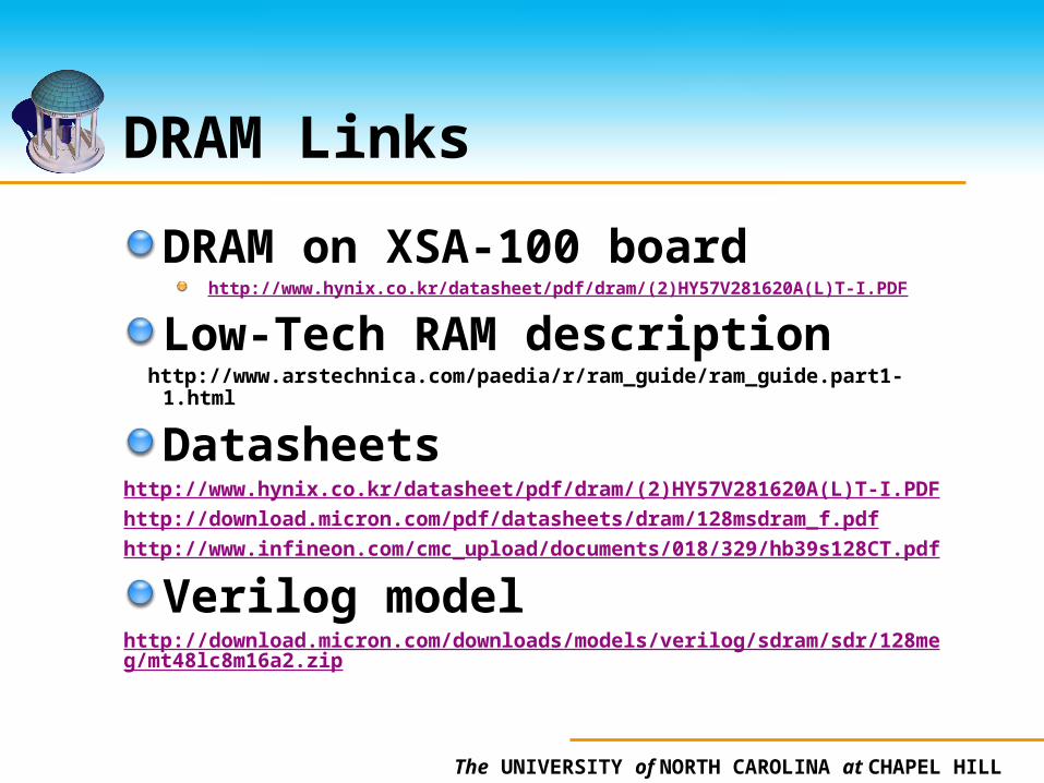
DRAM Links
DRAM on XSA-100 boardhttp://www.hynix.co.kr/datasheet/pdf/dram/(2)HY57V281620A(L)T-I.PDF
Low-Tech RAM description http://www.arstechnica.com/paedia/r/ram_guide/ram_guide.part1-
1.html
Datasheetshttp://www.hynix.co.kr/datasheet/pdf/dram/(2)HY57V281620A(L)T-I.PDFhttp://download.micron.com/pdf/datasheets/dram/128msdram_f.pdfhttp://www.infineon.com/cmc_upload/documents/018/329/hb39s128CT.pdf
Verilog modelhttp://download.micron.com/downloads/models/verilog/sdram/sdr/128meg/mt48lc8m16a2.zip

The UNIVERSITY of NORTH CAROLINA at CHAPEL HILL
Assignment
Try Block RAMMaybe to scan small stampsOr as character/sprite device
Make DRAM controller to refresh screenDeadline – end of next week

The UNIVERSITY of NORTH CAROLINA at CHAPEL HILL
Next Time
Thursday 9/11 read Kurt Akeley, "Reality Engine Graphics", SIGGRAPH 93
Link ishttp://doi.acm.org/
10.1145/166117.166131