THE STUDY OF CMOS BASED VCO WITH ACTIVE INDUCTOR AND …
72
THE STUDY OF CMOS BASED VCO WITH ACTIVE INDUCTOR AND ITS DESIGN METHODOLOGY By SY-MIN CHUENG A thesis submitted to the Graduate School-New Brunswick Rutgers, The State University of New Jersey in partial fulfillment of the requirements for the degree of Master of Science Graduate Program in Electrical and Computer Engineering written under the direction of Jeffrey Walling and approved by ________________________ ________________________ ________________________ ________________________ New Brunswick, New Jersey October 2012
Transcript of THE STUDY OF CMOS BASED VCO WITH ACTIVE INDUCTOR AND …
THE STUDY OF CMOS BASED VCO WITH ACTIVE INDUCTOR
AND ITS DESIGN METHODOLOGY
By
SY-MIN CHUENG
A thesis submitted to the
Graduate School-New Brunswick
Rutgers, The State University of New Jersey
in partial fulfillment of the requirements
for the degree of
Master of Science
Graduate Program in Electrical and Computer Engineering
written under the direction of
Jeffrey Walling
and approved by
________________________
________________________
________________________
________________________
New Brunswick, New Jersey
October 2012

© 2012
Sy-Min Chueng
ALL RIGHTS RESERVED
ABSTRACT OF THE THESIS
THE STUDY OF CMOS BASED VCO WITH ACTIVE INDUCTOR AND ITS DESIGN METHODOLOGY
By Sy-Min Chueng
Thesis director : Jeffery Walling
Active Inductors are useful in reducing the large chip area typically consumed by
spiral inductors, as well as providing larger inductance values and higher quality factors
that otherwise cannot be achieved by spiral inductors. Integrated inductors find
application in many radio frequency (RF) front end integrated circuits, including
impedance matching, filtering, biasing and in oscillator circuits. Nonetheless, because of
the interdependent relationship of the self-resonant frequency and quality factor it is
often difficult to meet desired circuit requirements. Additionally, active devices pose
problems of higher power consumption , noise figure and potential instability. This thesis
begins with the study of active inductors, the Wu active inductor in particular, and
considers tuning methods based on the Wu active inductor topology. Starting with the
small-signal model, the emulated inductance and quality factor expressions are derived.
Next, the operation of active inductors under large-signal is closely examined.
ii

Comparisons between a passive and an active VCO are made. The active inductor based
voltage-controlled oscillator (Active VCO) is studied extensively, and the methods of
improving the performance under large signal-behavior are discussed. Then a design
procedure based on gm/ID methodology is proposed. A Matlab script that can be applied to
gyrator-C based active inductors is developed to determine the sizing of the transistors for
a desired inductance and resonant frequency. Cadence Virtuoso is used for simulations,
and extraction based on an IBM 8RF technology file. Finally, a low power active VCO is
designed, simulated and laid out.
iii

Acknowledgements
I would like to thank my thesis advisor Prof. Jeffery Walling for his constant
guidance throughout the course of my thesis. His knowledge and insight into electrical
engineering are sources of inspiration. Most importantly, he has always been patient and
helpful when I encountered difficulty. He also contributed greatly to this work by sharing
his Ocean Script and Matlab codes for creating the technology file and the look-up
functions, as well as helping me revising the thesis thoroughly.
I would also like to thank Prof. Wei Jiang and Prof Predrag Spasojevic for being a
part of my thesis committee. I have taken both their classes when I was an undergraduate
student, and they are both very good professors. Special thanks to Prof. Wei. Jiang for
recommending me for graduate study at Rutgers. I hope my time spent in Rutgers ECE
program will help me become a competent engineer.
The appreciation is also given to the members of the group, Sumati Sehajpal and
Ilya Chigirev, for the discussion and help. Yi Huang also gave me many valuable inputs.
Finally, I want to thank my family and my parents for their moral and financial
support. Without them, I wouldn't have the opportunity to achieve this personal goal.
iv

Table of ContentsABSTRACT OF THE THESIS...........................................................................................iiAcknowledgements............................................................................................................iiiChapter 1..............................................................................................................................1
1.1 Introduction ..............................................................................................................1Chapter 2..............................................................................................................................3
2.1 Active Inductor..........................................................................................................32.2 Active Inductor Tuning.............................................................................................82.3 Negative Resistance Tuning....................................................................................11
Chapter 3............................................................................................................................163.1 Active VCO.............................................................................................................163.2 Voltage Swing.........................................................................................................203.3 Large Signal Analysis..............................................................................................233.4 Noise.......................................................................................................................353.5 Oscillator Phase Noise............................................................................................36
3.5.1 Injection Locked Active VCO.........................................................................363.5.2 Constant Q active Inductor..............................................................................37
Chapter 4............................................................................................................................394.1 Active Inductor Design...........................................................................................394.2 Active VCO Design.................................................................................................47
Chapter 5............................................................................................................................535.1 Conclusion and Further Work.................................................................................53
References..........................................................................................................................54Appendix A:The Derivation of equations 2.2~2.5 ............................................................58Appendix B: Matlab Code for Calculation of Active Inductor and VCO..........................60
v
List of FiguresFigure 1.1 Schematic diagram of a gyrator based active inductor.......................................2figure 2.1 Wu inductors with different types of feedback networks....................................3Figure 2.2 Small-Signal Model of an Active Inductor........................................................4Figure 2.3 Active Inductor and Its equivalent circuit..........................................................5Figure 2.4 Frequencies response of an active inductor........................................................7Figure 2.5 Schematic diagrams for active Inductors using negative feedbacks .................8Figure 2.6 (a) Inductance vs. frequency of Figure 2.5(a)..................................................10Figure 2.6 (b) Inductance vs. frequency of Figure 2.5(b)..................................................10Figure 2.7 Negative-resistance tuning...............................................................................11Figure 2.8 Active inductor with a negative-resistance circuit............................................12Figure 2.9 (a) Real part of the frequency response ...........................................................13Figure 2.9 (b) Imaginary part of the frequency response...................................................14Figure 2.10 Schematic for independent tuning..................................................................15Figure 3.1 Feedback system...............................................................................................16Figure 3.2 Frequency Selective network...........................................................................17Figure 3.3 Cross-coupled pairs..........................................................................................17Figure 3.4 Schematic for NMOS and PMOS voltage-controlled oscillators.....................18Figure 3.5 schematic for active VCO................................................................................19Figure 3.6 Typical output waveforms of PMOS and NMOS VCOs..................................20Figure 3.7 Large-signal voltage swing...............................................................................23Figure 3.8 Signal swing between regions of operation......................................................25Figure 3.9 Average Capacitance........................................................................................28Figure 3.10 An Active Inductor with Sine Wave at Its Input.............................................28Figure 3.11 Time-varying parameters under large-signal..................................................30Figure 3.12 Resonant frequency vs. time. The frequency of input sine-wave is 3GHz....34Figure 3.13 Equivalent noise circuit..................................................................................35Figure 3.14 A constant Q active inductor...........................................................................38Figure 4.1 (a) Vov vs. gm/Id.............................................................................................41Figure 4.1 (b) gm/Id vs. Id/W...........................................................................................41Figure 4.2 Schematic for creating technology file.............................................................42Figure 4.3 Active inductor ................................................................................................44Figure 4.4 Schematic for Active VCO...............................................................................49Figure 4.5 (a) Output voltage of Active VCO....................................................................50Figure 4.5 (b) Output current of active VCO.....................................................................51Figure 4.6 Complete layout................................................................................................52
vi
List of TablesTable 2.1 Sizing of the Transistors.......................................................................................8Table 3.1 Resonant frequency for Different Amplitudes and Sweeping Frequencies.......32Table 4.1 List of look up functions....................................................................................42Table 4.2 Transistors Sizing of Active VCO......................................................................50
vii
1
Chapter 1
1.1 Introduction Active inductors have gained great interests in low-power applications over the
last decade in an effort to reduce the need for large chip area required to fabricate spiral
inductors and transformers. Inductive impedances are essential in high speed application
due to their ability to improve bandwidth and boost gain, and to perform impedance
matching and frequency selection. Many architectures for active inductors have been
proposed [1-6]. Some of the unique advantages of active devices compared to those of
their passive counterparts are small layout area, larger inductance and quality factor with
the ability to tune either parameter, and full compatibility with digitally oriented CMOS
technologies. Nonetheless, active inductors have several drawbacks including: higher
power consumption for biasing the transistors, relatively low power handling capability
since the active inductors do not have the energy storage properties of physical inductors,
higher noise figure owing to active components and limited bandwidth due to the active
devices. Additionally, one side of the active inductor being always held at a constant DC
bias restricts the possible applications. All these make active inductors difficult to
integrate.
Active inductors are based on the gyrator principle. A symbol representing such
inductors is shown in Figure 1.1. The forward path transconductor, G, has a positive
transconductance while the transonductor in the feedback path, -G, has a negative
transconductance. Inductance is simulated by the capacitance C. For this reason, the

2
synthesized inductor is called a gyrator-C active inductor with an inductance value [7]
Figure 1.1 Schematic diagram of a gyrator based active inductor.
C/G2 (1.1)
where G is the gyration conductance. Cascading two ideal gyrators forms an ideal
transformer suggests that two active inductor can be electrically coupled to form an
active transformer. [8] The focus of this thesis is to study the Wu current-reuse active
inductor[9], as well as its applications; specifically, the CMOS differential LC oscillator
will be examined. First the small signal equivalent circuit will be examined, and then this
knowledge will be expanded to predict the large signal behavior of the active inductor in
an active-LC VCO. Finally, after considering many design issues, the goal is to create a
procedure to design the active VCO systematically.
G
-GC
Vin

3
Chapter 2
2.1 Active Inductor
(a) (b) (c)
figure 2.1 Wu inductors with different types of feedback networks.
Three types of shunt-feedback active inductors shown in (Figure 2.1) were
proposed in Wu's paper [9]. All operate in a similar manner. In Figure 2.1(a) the input
signal at the drain of M1 generates a current gm2vi , that charges Cgs1 through the feedback
path. The voltage vx then provides for the current gm1vgs1 and generates an inductive
loading effect. Shown in Figure 2.1(b), R , and current source, Ir , form a DC level shifter.
The shunt capacitance acts to short the resistor at high frequencies. In Figure 2.1(c),
transistors M3 and M4 are used as level shifter similar to (b). Another way to look at this
is that at low frequencies the impedance at the input node is low due to the shunt
feedback as the frequency increases, the current starts to flow through the gate-source
capacitance and causes the loop gain to reduce. Hence, the impedance increases as the
frequency increases, emulating the impedance of an inductor [10].
4
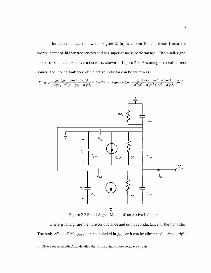
The active inductor shown in Figure 2.1(a) is chosen for this thesis because it
works better at higher frequencies and has superior noise performance. The small-signal
model of such an the active inductor is shown in Figure 2.2. Assuming an ideal current
source, the input admittance of the active inductor can be written as1:
(2.1)
Figure 2.2 Small-Signal Model of an Active Inductor
where gm and go are the transconductance and output conductance of the transistor.
The body effect of M2, gmb2, can be included in gm2 , or it can be eliminated using a triple
1 Please see Appendix A for detailed derivation using a more complete circuit
Y =go1gm1gm2go2 sCgd 1
sCgd 2sCgs1go2sCgd 1sCgs2gm2go2sCgd 1−
go2gm2go2sCgd1sCgd2sCgs1go2sCgd 1
gm2v2 go2cds2
cdg2
cgs2
v1
go1
cds1
cdg1
cgs1
+
-
go3
cdd3
v2
+
-VIn
IIN
5
well structure. Cdd3 and go3 are zero for an ideal current source and Cds1 and Cds2 are
neglected since they are likely to be small when the transistors are saturated. The input
impedance is given by [3]:
Z ln=b1 sbo
s22αsω02 (2.2)
b1=1
C gs2, b0=
go2
C gs1C gs2(2.3)
2α=go1C gs1go2 Cgs2gm2 C gs1go2Cgs1
C gs1 C gs2 (2.4)
ω02=
gm1 gm2gm1 go2go1 go2
Cgs1 C gs2
(2.5)
where ωo is the resonant frequency of the active inductor. The quality factor is defined by
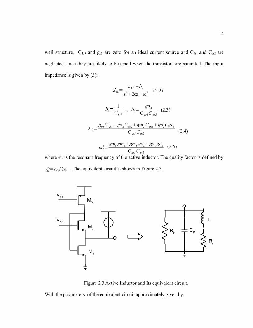
. The equivalent circuit is shown in Figure 2.3.
Figure 2.3 Active Inductor and Its equivalent circuit.
With the parameters of the equivalent circuit approximately given by:
L
Rs
CPRP
M1
M2
M3
Vb1
Vb2
Q=ωo/ 2α
6
C P=C gs2 (2.6)
RP=1
gm2(2.7)
RS=go2go3
gm1 gm2(2.8)
L=Cgs1Cgd1Cgd2
gm1 gm2(2.9)
From (6)-(9), it can readily be shown that changing the bias currents and aspect
ratios of the transistors, the inductance value, center frequency and quality factor can be
varied.
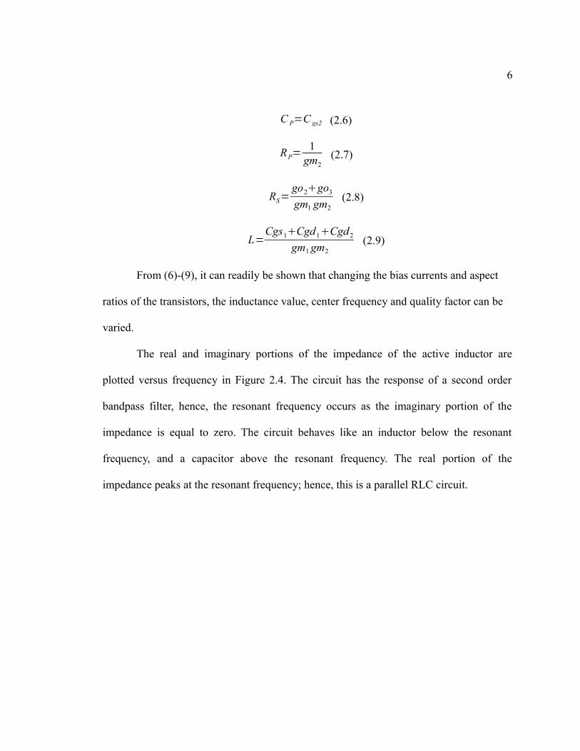
The real and imaginary portions of the impedance of the active inductor are
plotted versus frequency in Figure 2.4. The circuit has the response of a second order
bandpass filter, hence, the resonant frequency occurs as the imaginary portion of the
impedance is equal to zero. The circuit behaves like an inductor below the resonant
frequency, and a capacitor above the resonant frequency. The real portion of the
impedance peaks at the resonant frequency; hence, this is a parallel RLC circuit.

7
Figure 2.4 Frequencies response of an active inductor.
8
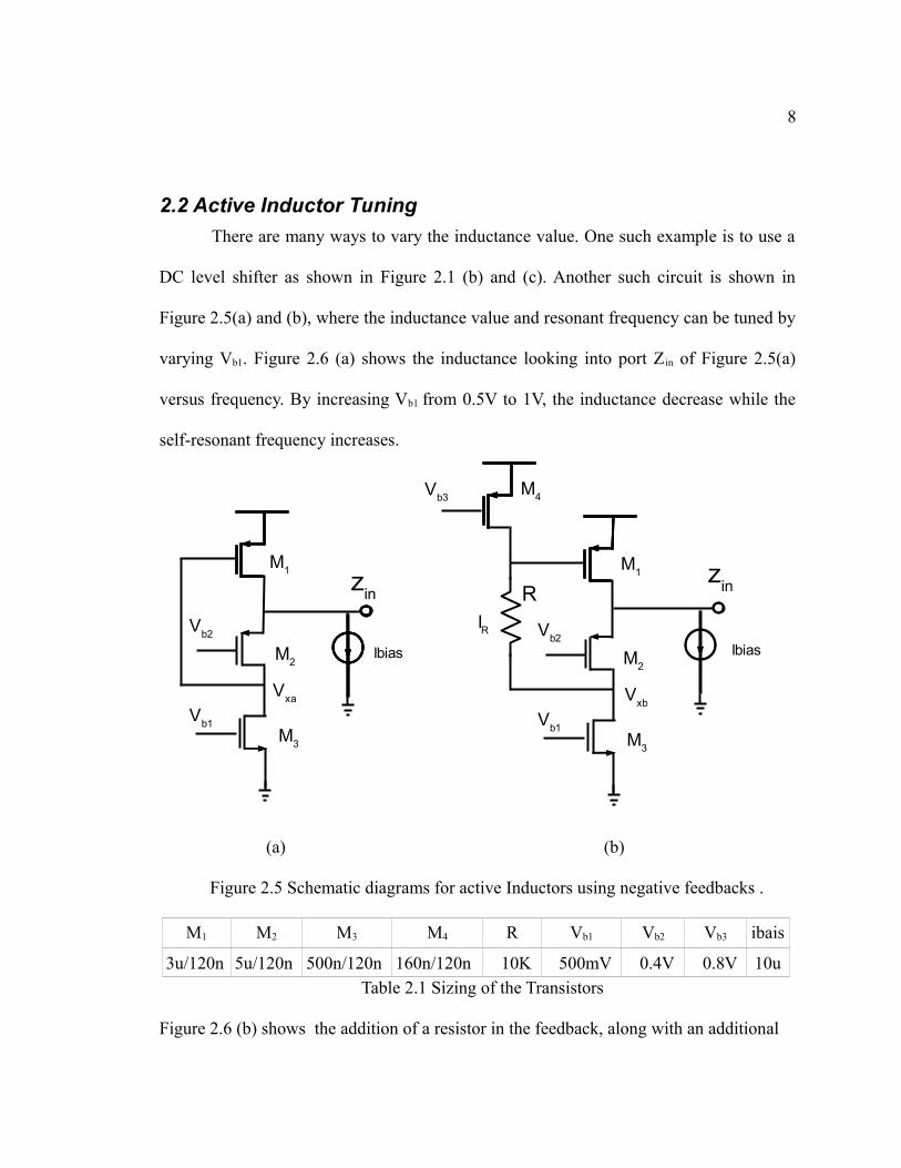
2.2 Active Inductor TuningThere are many ways to vary the inductance value. One such example is to use a
DC level shifter as shown in Figure 2.1 (b) and (c). Another such circuit is shown in
Figure 2.5(a) and (b), where the inductance value and resonant frequency can be tuned by
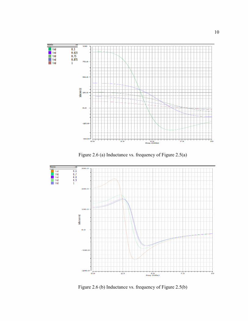
varying Vb1. Figure 2.6 (a) shows the inductance looking into port Z in of Figure 2.5(a)
versus frequency. By increasing Vb1 from 0.5V to 1V, the inductance decrease while the
self-resonant frequency increases.
(a) (b)
Figure 2.5 Schematic diagrams for active Inductors using negative feedbacks .
M1 M2 M3 M4 R Vb1 Vb2 Vb3 ibais
3u/120n 5u/120n 500n/120n 160n/120n 10K 500mV 0.4V 0.8V 10uTable 2.1 Sizing of the Transistors
Figure 2.6 (b) shows the addition of a resistor in the feedback, along with an additional
M3
M2
M1
Vb2
Vb1
M4Vb3
M3
M2
Vb2
Vb1
M1
Ibias Ibias
zinzin
IR
R
Vxa Vxb
9
current source;in this topology. the inductance can be greatly increased while marginally
reducing the resonant frequency.
In Figure 2.5(a), Vsg1 is given by VDD-Vxa , while in in Figure 2.5(b), Vsg1 is equal
to VDD -IR*R + Vxb, where
I R=12
μp C oxWLV sg−∣V T∣
2 (2.10)
ID1 in both cases is given by ibias+ID3, so gm remains constant if the region of operation does
not change. In Figure 2.5(a). ID2 = ID3, whereas in Figure 2.5(b), ID2=ID3-IR . This implies
that M2 need not provide as much current in the latter case as it does in the former case,
thus the gm2 in case 2 is reduced. From (2.9), we can see that this reduction in gm2 results
in an increased effective inductance L.
Additionally, passive capacitors and inductors can be used in combination with
the active inductor to enhance the circuit performance. For example, by adding a physical
inductor at Zin in series, the inductance increases by the value of the physical inductor, or
by adding a capacitance between source and gate of M1 , the increase in CGS1 also
increases the inductance value as it can be seen in (2.9). However, adding a passive
inductor in series with the active inductor tends to increase the voltage swing which
adversely affects the stability of the DC bias.
10
Figure 2.6 (a) Inductance vs. frequency of Figure 2.5(a)
Figure 2.6 (b) Inductance vs. frequency of Figure 2.5(b)
11
2.3 Negative Resistance TuningBy neglecting the output conductance from expressions (2.4) and (2.5), the
relations for resonant frequency and quality factor are attained:
ω0≈ gm1 gm2
Cgs1C gs2=ωt1ω t2
; Q0≈ gm1 C gs2
gm2C gs1= ωt1
ωt2
(2.10)
where ωt is the transition frequency of the transistor. If two transistors are of similar size,
the Q of the inductor is approximately unity. Because of the interdependence of these
two parameters in (2.10), one cannot be changed independently of the other. In practice,
the series parasitic resistance, RS, also serves to decrease the quality factor of inductor.
From (2.8), it can be seen that by maintaining high transistor output resistance (e.g. ,
go2=go3=0.) the series resistance can be reduced. However, as the bias current increases
the resonant frequency, the output resistance similarly increases [11].
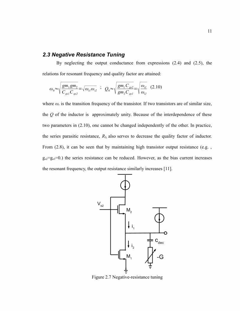
Figure 2.7 Negative-resistance tuning
M1
M2
Vb2
i1
i2cdec
-G
12
Use of a negative resistance, as shown in Figure 2.7, improves the Q of the active
inductor.
As shown in Figure 2.7, Cdec is a decoupling capacitance, it should be large enough
to not adversely affect the frequency response, while decoupling the negative
transconductance -G from the DC bias of the active inductor. While the negative
resistance strongly increases the quality factor, the resonant frequency decreases at the
same time. Expressions (4) and (5) now become [12]:
2α=go1C gs1go2 Cgs2gm2 C gs1go2Cgs1−G Cgs1
C gs1 C gs2(11)
ω02=
gm1 gm2gm1 go2go1 go2−G go2
Cgs1C gs2
(12)
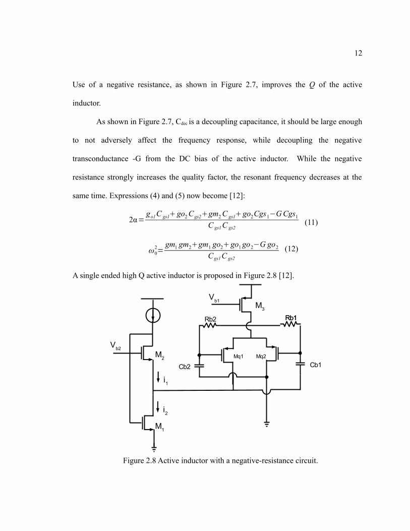
A single ended high Q active inductor is proposed in Figure 2.8 [12].
Figure 2.8 Active inductor with a negative-resistance circuit.
M1
M2
Vb2
i1
i2
M3
Vb1
Rb1Rb2 Rb1
Cb1Cb2Mq1 Mq2
13
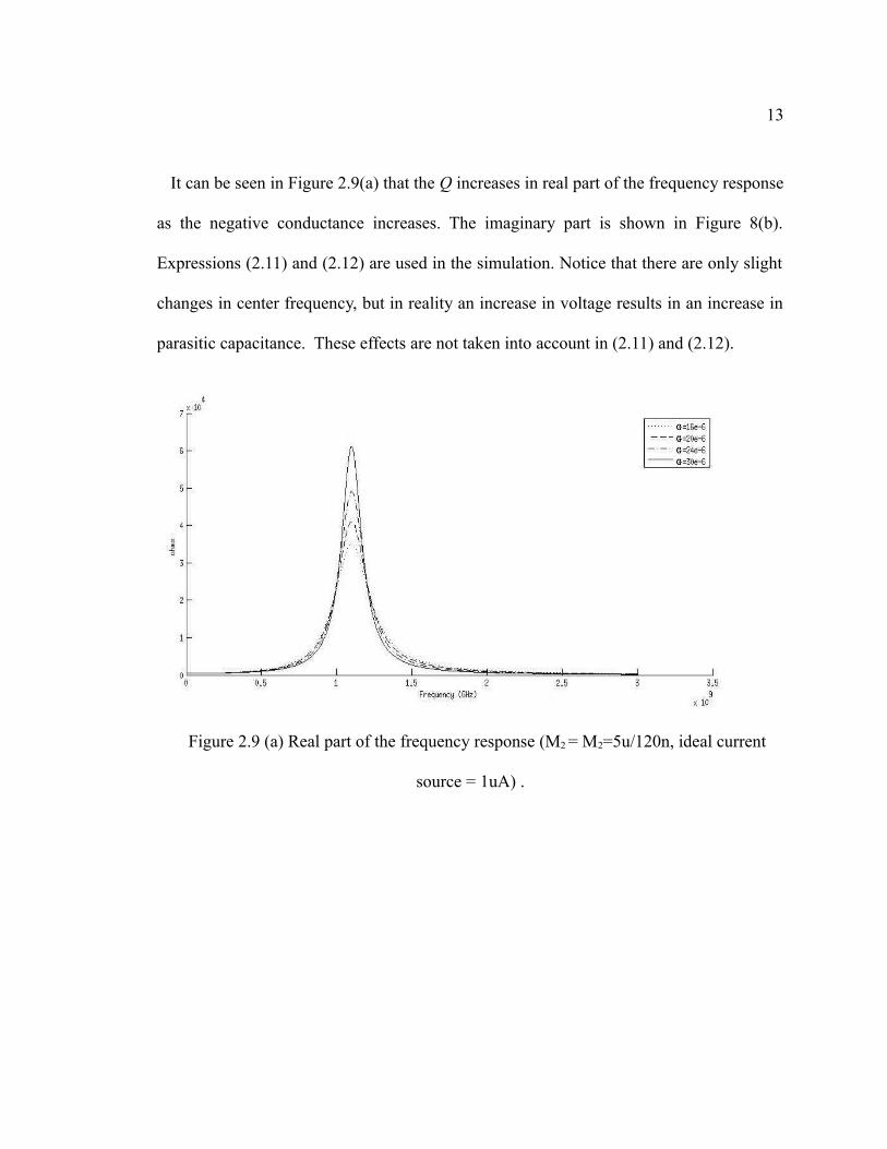
It can be seen in Figure 2.9(a) that the Q increases in real part of the frequency response
as the negative conductance increases. The imaginary part is shown in Figure 8(b).
Expressions (2.11) and (2.12) are used in the simulation. Notice that there are only slight
changes in center frequency, but in reality an increase in voltage results in an increase in
parasitic capacitance. These effects are not taken into account in (2.11) and (2.12).
Figure 2.9 (a) Real part of the frequency response (M2 = M2=5u/120n, ideal current
source = 1uA) .
14
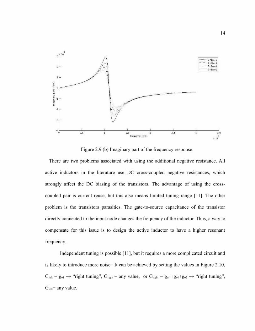
Figure 2.9 (b) Imaginary part of the frequency response.
There are two problems associated with using the additional negative resistance. All
active inductors in the literature use DC cross-coupled negative resistances, which
strongly affect the DC biasing of the transistors. The advantage of using the cross-
coupled pair is current reuse, but this also means limited tuning range [11]. The other
problem is the transistors parasitics. The gate-to-source capacitance of the transistor
directly connected to the input node changes the frequency of the inductor. Thus, a way to
compensate for this issue is to design the active inductor to have a higher resonant
frequency.
Independent tuning is possible [11], but it requires a more complicated circuit and
is likely to introduce more noise. It can be achieved by setting the values in Figure 2.10,
Gleft = go1 → “right tuning”, Gright = any value, or Gright = gm1+go1+go2 → “right tuning”,
Gleft= any value.
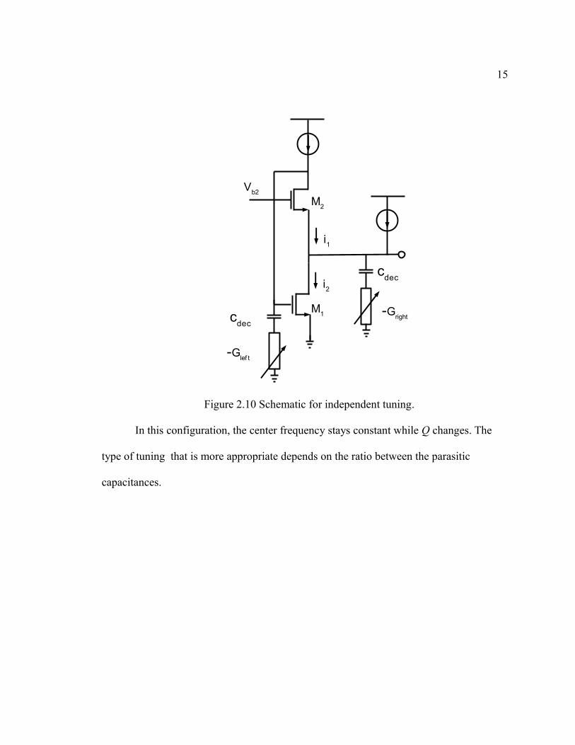
15
Figure 2.10 Schematic for independent tuning.
In this configuration, the center frequency stays constant while Q changes. The
type of tuning that is more appropriate depends on the ratio between the parasitic
capacitances.
M1
M2
Vb2
i1
i2cdec
-Grightcdec
-Glef t

16
Chapter 3
3.1 Active VCOIn order for oscillation to start, the Barkhausen stability criteria must be satisfied. For a
system configured in feedback (e.g., Figure 3.1), oscillation will occur at the frequency,
ω0 , where the magnitude of the loop transfer function, |H(jω0) | ≥ 1 and the phase of the
transfer function is H( jω∠ 0) = 180o . Simply satisfying the Barkhausen criteria does not
guarantee oscillation, due to oscillation startup requirements. Hence, typically, the loop
gain is chosen to be approximately 2-3 times the required values to guarantee startup
[27].
Figure 3.1 Feedback system.
Note that the transfer function, H(s), is designed to produce 180o of phase shift in
the forward signal path, and the additional 180o phase shift is achieved through negative
feedback; the total phase shift around the loop must be an integer multiple of 360o. In
many RF oscillators, a frequency selective network (e.g., LC tank) is included in part of
loop as shown in Figure 3.2.
Because the gain of an LC filter rolls off at frequencies outside the resonant frequency,
the Barkhausen criteria is only satisfied for systems operating at the resonant frequency.
++
-x(s) Y(s)H(s)

17
For a lossy LC resonant tank, energy is dissipated in the parasitic resistance associated
with the components, hence, a negative resistance is added in parallel with the
Figure 3.2
LC tank to compensate for the loss from the tank. In other words, additional
energy is provided by an active circuit in order to sustain the oscillation. The negative
resistance serves two purposes. First, for oscillation to begin, the circuit needs sufficiently
large voltage gain. Second the oscillation amplitude continues to grow until the loop gain
reduces at the peak voltage swing of the signal. For a practical circuit, the negative
resistance should be two to three times higher than the resistance of the LC tank to
account for process variation, supply voltage fluctuation, and temperature drift (PVT) [7].
The most commonly used negative-GM topology for a differential oscillator is the cross-
Figure 3.3 Cross-coupled pairs.
++
-x(s) Y(s)H(s)
Frequency selective network
M1 M2
zin
18
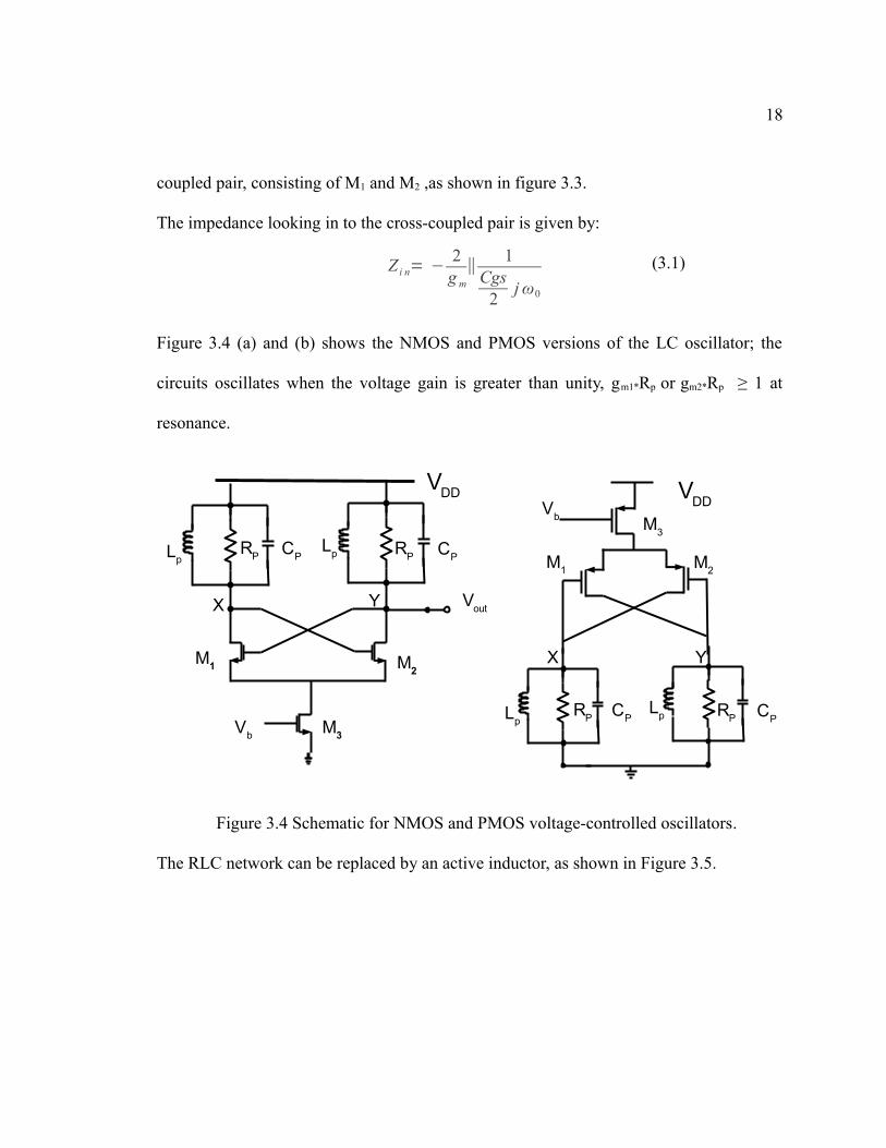
coupled pair, consisting of M1 and M2 ,as shown in figure 3.3.
The impedance looking in to the cross-coupled pair is given by:
(3.1)
Figure 3.4 (a) and (b) shows the NMOS and PMOS versions of the LC oscillator; the
circuits oscillates when the voltage gain is greater than unity, gm1*Rp or gm2*Rp ≥ 1 at
resonance.
Figure 3.4 Schematic for NMOS and PMOS voltage-controlled oscillators.
The RLC network can be replaced by an active inductor, as shown in Figure 3.5.
Z i n= − 2g m
∥ 1Cgs
2 j ω0
LpCPRP
Lp CPRP
VDD
M1 M2
VoutX Y
M3Vb
LpCPRP
Lp CPRP
X Y
M1 M2
M3
Vb
VDD

19
Figure 3.5 schematic for active VCO.
M1
M2
M3
Vb1
Vb2
M4
Vb1
Vb2
M7 M8
M9
Vb3
M3
Vb1
M5
M6
x yIx Iy
20
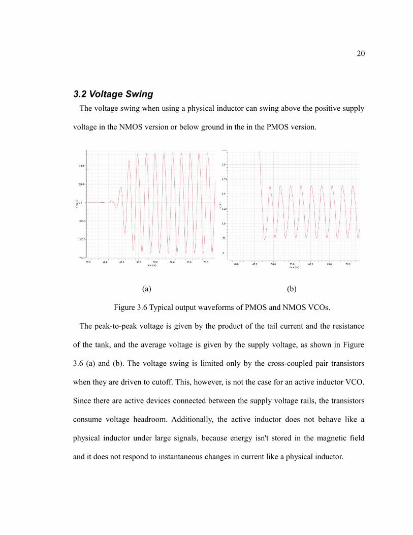
3.2 Voltage SwingThe voltage swing when using a physical inductor can swing above the positive supply
voltage in the NMOS version or below ground in the in the PMOS version.
(a) (b)
Figure 3.6 Typical output waveforms of PMOS and NMOS VCOs.
The peak-to-peak voltage is given by the product of the tail current and the resistance
of the tank, and the average voltage is given by the supply voltage, as shown in Figure
3.6 (a) and (b). The voltage swing is limited only by the cross-coupled pair transistors
when they are driven to cutoff. This, however, is not the case for an active inductor VCO.
Since there are active devices connected between the supply voltage rails, the transistors
consume voltage headroom. Additionally, the active inductor does not behave like a
physical inductor under large signals, because energy isn't stored in the magnetic field
and it does not respond to instantaneous changes in current like a physical inductor.
21
For the circuit in Figure 3.5, the minimum output voltage of Vx occurs when Ix is zero,
where M8 is in cutoff, assuming M1 and M2 are in saturation. Ignoring the threshold
voltages difference due to body effect and equating the current yields:
12
μn CoxWL 1
V GS1−V Tn2=1
2μn CoxW
L 2V GS2−V Tn
2 (3.2)
Dividing both side by (W/L)2 , and replacing VGS2 by (Vb2–Vxmin) , where Vb2 is the bias
voltage yields:
√(W / L )1(W /L )2
(V GS1−V Tn)=V b2−V xmin−V Tn (3.3)
V xmin=V b2−√(W /L )1(W /L )2
V GS1+V Tn(1+√(W /L )1(W /L )2) (3.4)
because the drain current, ID, of M1 , M2 and M3 are the same , VGS1 can be expressed in
term of ID ;
V GS1= 2 I D
μ p Cox
W 3
L
∣V T∣ (3.5)
Additionally, the phase difference between the differential outputs is 180o . When Vx is
at its minimum voltage, Vy is at its maximum. For simplicity, assume M9 is operating in
saturation, and M7 is operating in triode. This gives:
V ymax=V DD−V OV9−V DS7 (3.6)
where
V OV9=V DD−V b3−∣V T∣ (3.7)
Since M8 is cutoff, all biasing current is conducted through M7:
22
12
μ pC ox(WL )9 V OV9
2 = μ pC ox(WL )7((V SG7−∣V Tp∣)V SD7−
V SD72
2 ) (3.8)
Simplifying the expression yields:
WL 9
V OV92 =W
L 72V SG7−∣V Tp∣V SD7−V SD7
2 (3.9)
and write the quadratic equation in term of VSD7
V SD72 −2V OV7 V SD7
W /L 9W /L 7
V OV92 =0 (3.10)
where:
V OV7=V SG7−∣V Tp∣=V DD−V OV9−Vxmin−∣V Tp∣ (3.11)
VSD7 can be solved for:
V SD7=2 V OV7± 4V OV7
2 −4W /L 9W /L 7
V OV92
2=V OV7±V OV7
2 −W /L 9W /L 7
V OV92 (3.12)
Since the transistor is in triode, that means VOV > VDS , hence the solution that satisfies
this condition is chosen:
(3.13)
This shows that as the size of the cross-coupled pair increases, the voltage drop VSD7
decreases.
V SD7=V OV7−√V OV72 −
(W / L )9(W / L )7
V OV92

23
3.3 Large Signal AnalysisWhile the equivalent RLC circuit accurately describes the small-signal behavior of the
active inductor, it does not apply to the large-signal behavior due to the dependence on
the transistors DC bias condition and the maximum signal swing of the active inductor
[14-15]. The transconductance decreases as the signal-swing increases, and the resonant
frequency decreases as a result. Because the transconductance and capacitance of the
transistors are time varying Fourier series analysis is used to examine the large-signal
behavior. It should be expected that the large signal Gm, and Cavg are the weighted
averages of the small-signal gm and C over the varying DC bias condition with respect to
time of the transistors.
Figure 3.7 Large-signal voltage swing.
For an NMOS operating in the saturation region on a small-signal, as shownin Figure
3.7, the large-signal GM is the same as the small-signal gm. [14] To see this, the drain
current in the saturation region is given by:
M1
V1cos(ωt)
vGSQ
vTH vin1 vi
n
gm

24
I D=12
μn Cox WLV T
2 V GS
V T−1
2
(3.14)
where VGS = VGS Q + V1 cos(ωt), IDSS =12
μn Cox WLV T
2 , and VTH < VGS <Vin1.
Equation (3.14) can be rewritten as:
I D=I DSS V GSQV 1 cos ωt
V T−1
2
=I DSS
V T2 V GSQV 1 cos ωt −V T
2 (3.15)
Substitution of VX = VGSQ – VT , and expansion of (3.15) as a Fourier series yields:
I D=I DSS
V T2 V X
2 −2VX V 1 cos ωt V 12 cos ωt 2 (3.16)
I D=I DSS
V T2 V X
2 V 1
2
2−2VX V 1 cos ωt
V 12
2cos 2ωt (3.17)
The DC term is given by
I o=I DSS
V T2 V X
2 V 1
2
2 (3.18)The second term is I 1=−2
I DSS
V T2 V X V 1 (3.19)
Ignore the higher order term, and the large-signal, Gm,is defined as
Gm=I 1
V 1=−2
I DSS
V T2 V X=2
I DSS
V T2 V GSQ−V T =k ' w
LV GSQ−V T =gm (3.20)
This suggests the large-signal Gm is the same as the small-signal gm as long as the
transistor is in saturation. However, if the transistor is switching between cutoff and
saturation, as shown Figure 3.8, the large-signal Gm will be smaller than the small-
signal gm.
25
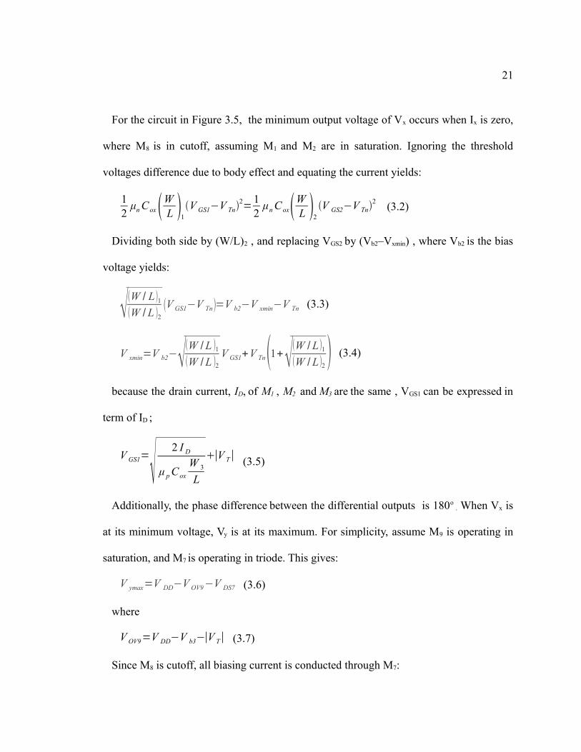
Figure 3.8 Signal swing between regions of operation
If φ is defined to be the conduction angle cosφ=V X
V 1, the Fourier series analysis of
the signal for the fundamental frequency is derived in [14]:
I 1=
2I p
π
34
sin φ 112
sin 3φ−φ cosφ
1−cosφ2(3.21)
where IP is the peak voltage of ID :
I p=I DSS
V T2 V 1−V X
2 (3.22)
The relation of the large signal Gm is given by
Gm=I 1
V 1=
2 I DSS I 1
I p
−2V 1
V T
=gmo
I 1
I p
−2V 1
V T
(3.23)
vTH vin1 vin
2φ
iD
IDSS
2φ
2φ
vxIP

26
Here, it is assumed the transistor is cut off when VGS-VT < 0, however a more accurate
model such as the EKV model or BSIM model is necessary for the transistor operating in
the subthreshold region (e.g., in weak inversion) . An empirical expression of ID valid for
all region of operations proposed by the EKV model is given by [18]:
I D=2 N μn Cox WLU t
2[ ln1eV GS−V T
2U T ]= I S [ln1expV GS−V T
2U T ] (3.24)
where N is a device dependent parameter, Ut = kT/q and Is = 2NμnCox(W/L)Ut2
g m=I D∣1−e− ID/ IS ∣N U t I D/ I S
(3.25)
27
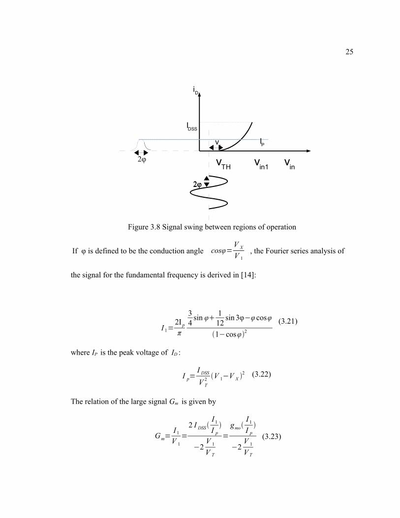
If the voltage swing is large, the large-signal capacitance is given by the weighted
average of the small-signal capacitance over one period of oscillation []. Because the
capacitance of the transistor is a function of voltage, a time-varying voltage swing causes
the capacitance to also be time-varying. The current-voltage relationship is then given by:
i=C v t d v t dt (3.26)
The fundamental frequency rms current can be calculated by determining the Fourier
coefficient.
an=12
2T ∫0
T
i t cos nω0tdt (3.27)
For an input voltage v(t)=Asin(ω0 t)+B, the large-signal average capacitance is given by:
C AVG=ω0
π ∫0
2πω0
[C Asin ω0 t Bcos ω0t ]cos ω0tdt (3.28)
This result can be computed numerically. Figure 3.9 shows the C-V characteristic curve
of an inversion mode NMOS. The dotted line represents the average capacitance at a
given voltage amplitude.

28
Figure 3.9 Average Capacitance.
To see the effect of a large-signal amplitude swing on the active inductors
resonant frequency, a test current source is connected to the input node as shown in
Figure 3.10. The current source consists of a DC bias and a large-signal sinusoid.
For a parallel RLC circuit, the resonance occurs at the frequency where the
impedance is maximum. To study the large-signal behavior, the transistors behavior at
Figure 3.10 An Active Inductor with Sine Wave at Its Input.
M1
M2
M3
Vb1
Vb2 I sinω t + IDC
29
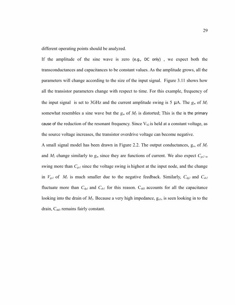
different operating points should be analyzed.
If the amplitude of the sine wave is zero (e.g., DC only) , we expect both the
transconductances and capacitances to be constant values. As the amplitude grows, all the
parameters will change according to the size of the input signal. Figure 3.11 shows how
all the transistor parameters change with respect to time. For this example, frequency of
the input signal is set to 3GHz and the current amplitude swing is 5 µA. The gm of M1
somewhat resembles a sine wave but the gm of M2 is distorted; This is the is the primary
cause of the reduction of the resonant frequency. Since Vb2 is held at a constant voltage, as
the source voltage increases, the transistor overdrive voltage can become negative.
A small signal model has been drawn in Figure 2.2. The output conductances, go, of M1
and M2 change similarly to gm since they are functions of current. We also expect Cgs2 to
swing more than Cgs1 since the voltage swing is highest at the input node, and the change
in Vgs1 of M1 is much smaller due to the negative feedback. Similarly, Cdg2 and Cds2
fluctuate more than Cdg1 and Cds1 for this reason. Cdd3 accounts for all the capacitance
looking into the drain of M3. Because a very high impedance, go3, is seen looking in to the
drain, Cdd3 remains fairly constant.
30
Figure 3.11 Time-varying parameters under large-signal

31
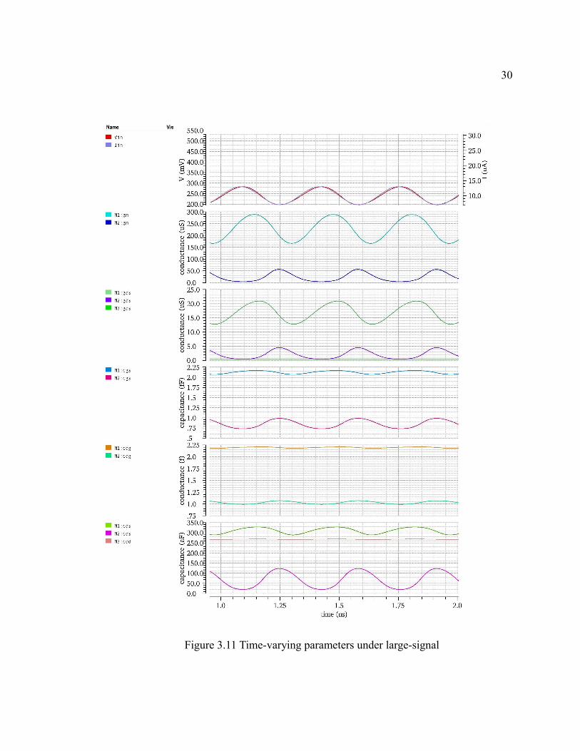
To examine the resonant frequency of the circuit, the “instantaneous resonant
frequency” ωo(t) can be numerically computed. After the result is obtained, it can then be
compared to the measurement result to decide how the resonant frequency should be
estimated. One thing to keep in mind is that, because of the nonlinear capacitance that is
dependent on frequency, the frequency being swept will affect the result. Furthermore,
time-varying capacitors distort the current waveform [17], so the transconductances are
also impacted. Nonetheless, to simplify the analysis, the frequency of the input is
maintained unchanged throughout the simulation.
Shown in Figure 3.12 is a plot from the transient analysis in Cadence SpectreRF,
and then exported to Matlab to obtain a similar figure to that shown in obtained in
Chapter 2. The last figure shows the average resonant frequency over 30 periods at each
amplitude. As expected, when the current swing is zero, it is seen that the resonant
frequency is time invariant. Between 0 and 1uA, the resonant frequency only reduces by
approximately 100 MHz, but it reduces more rapidly as the current amplitude increases.
This agrees with the analysis that the large-signal Gm diverges from the small-signal gm as
the transistor transitions between different regions of operation. It can be observed that
the waveforms appear less like sine waves as the amplitude is increased. The numerical
results are tabulated in table 3.1.

32
Table 3.1 Resonant frequency for Different Amplitudes and Sweeping Frequencies
Amplitude (uA) Sweeping Frequency(3.5GHz) Sweeping Frequency(3GHz) Sweeping Frequency(1GHz) Measurement0 3.1102467 3.1138655 3.1138655 3.151 3.0717220 3.0732560 3.1085358 3.062 2.9592346 2.9504856 3.0907238 2.933 2.7979444 2.7654732 3.0586686 2.714 2.6132728 2.5487988 3.0085847 2.565 2.4339291 2.3388632 2.9334426 2.486 2.1344696 2.1514546 2.8208732 2.367 2.1188016 1.9900242 2.6534550 2.168 1.9822391 1.8521528 2.4187026 2.009 1.8635719 1.7343766 2.1301333 1.85
10 1.7456735 1.6355452 1.8287985 1.59
33

34
Figure 3.12 Resonant frequency vs. time. The frequency of input sine-wave is 3GHz
35
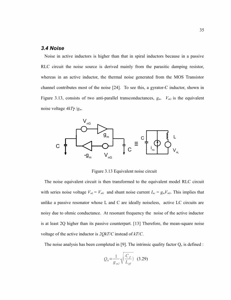
3.4 NoiseNoise in active inductors is higher than that in spiral inductors because in a passive
RLC circuit the noise source is derived mainly from the parasitic damping resistor,
whereas in an active inductor, the thermal noise generated from the MOS Transistor
channel contributes most of the noise [24]. To see this, a gyrator-C inductor, shown in
Figure 3.13, consists of two anti-parallel transconductances, gm. VnG is the equivalent
noise voltage 4kTγ /gm.
Figure 3.13 Equivalent noise circuit
The noise equivalent circuit is then transformed to the equivalent model RLC circuit
with series noise voltage VnL = VnG and shunt noise current Inc = gmVnG. This implies that
unlike a passive resonator whose L and C are ideally noiseless, active LC circuits are
noisy due to ohmic conductance. At resonant frequency the noise of the active inductor
is at least 2Q higher than its passive counterpart. [13] Therefore, the mean-square noise
voltage of the active inductor is 2QkT/C instead of kT/C.
The noise analysis has been completed in [9]. The intrinsic quality factor Qo is defined :
Q0=1
g m2√( C P
Leff) (3.29)
LC
-gm
gm
VnG
VnG
C C≡
inc VnL
36
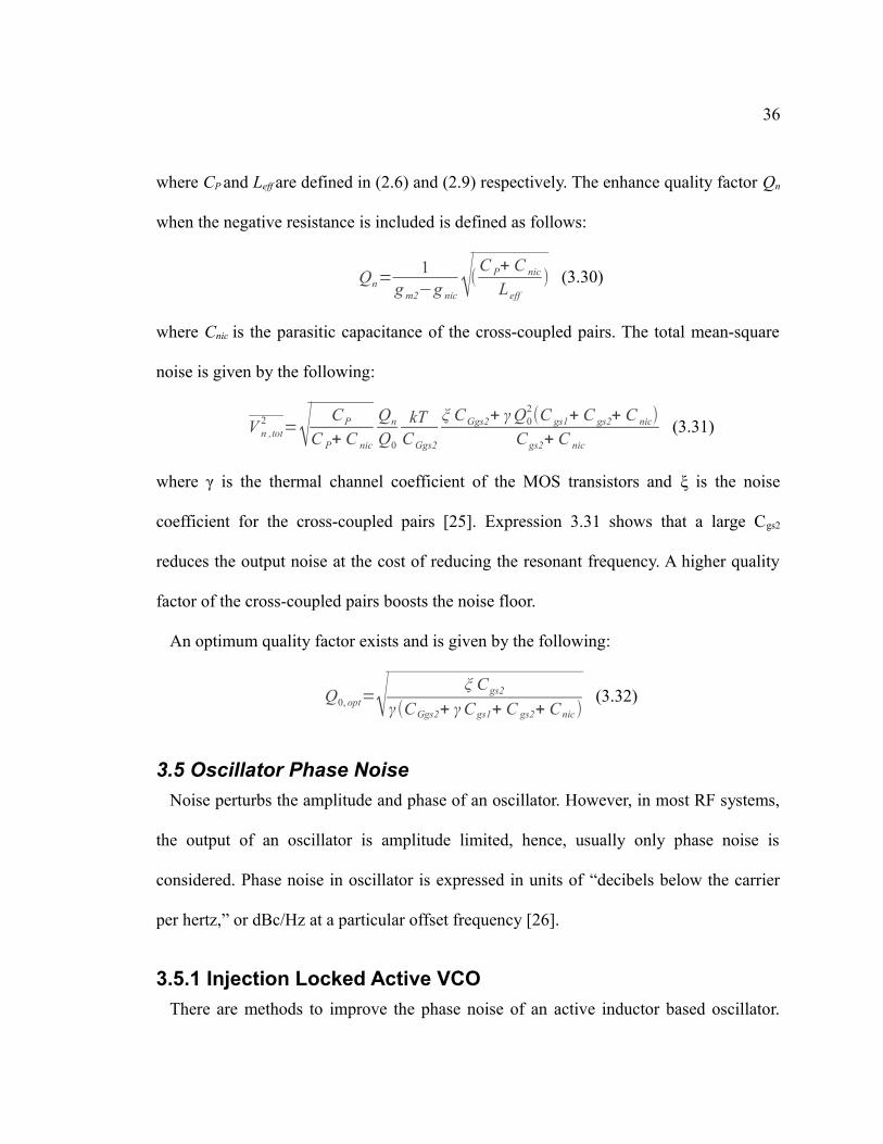
where CP and Leff are defined in (2.6) and (2.9) respectively. The enhance quality factor Qn
when the negative resistance is included is defined as follows:
Qn=1
g m2−g nic√(C P+ C nic
Leff) (3.30)
where Cnic is the parasitic capacitance of the cross-coupled pairs. The total mean-square
noise is given by the following:
V n ,tot2 =√ CP
C P+ C nic
Qn
Q0
kTCGgs2
ξ CGgs2+ γ Q02(C gs1+ C gs2+ C nic)
Cgs2+ C nic(3.31)
where γ is the thermal channel coefficient of the MOS transistors and ξ is the noise
coefficient for the cross-coupled pairs [25]. Expression 3.31 shows that a large Cgs2
reduces the output noise at the cost of reducing the resonant frequency. A higher quality
factor of the cross-coupled pairs boosts the noise floor.
An optimum quality factor exists and is given by the following:
Q0, opt=√ ξ Cgs2
γ (CGgs2+ γ Cgs1+ C gs2+ Cnic)(3.32)
3.5 Oscillator Phase NoiseNoise perturbs the amplitude and phase of an oscillator. However, in most RF systems,
the output of an oscillator is amplitude limited, hence, usually only phase noise is
considered. Phase noise in oscillator is expressed in units of “decibels below the carrier
per hertz,” or dBc/Hz at a particular offset frequency [26].
3.5.1 Injection Locked Active VCOThere are methods to improve the phase noise of an active inductor based oscillator.
37
The injection locked active inductor oscillator can have a lower phase noise level than
that of the external injecting signal [15]. A numerical example of a free running active
VCO that resonates at 2.4 GHz and consumes 1.1mW is given in [15]. It has a phase
noise of -70dBc/Hz at 1 MHz frequency offset. With the injection of a sinusoidal signal,
the phase noise of the active VCO improves to -118dBc/Hz at 1 MHz frequency offset.
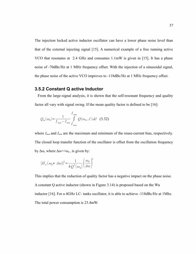
3.5.2 Constant Q active InductorFrom the large-signal analysis, it is shown that the self-resonant frequency and quality
factor all vary with signal swing. If the mean quality factor is defined to be [16]:
Qm(ω0)=1
I max− Imin∫
I max
I min
Q(ω0 , J )dJ (3.32)
where Imax and Imin are the maximum and minimum of the reuse-current bias, respectively.
The closed loop transfer function of the oscillator is offset from the oscillation frequency
by Δω, where Δω<<ωo , is given by:
∣H C(ω0+ Δω)∣2≈ 14Q 2(ω0)
( ω0
Δω)2
This implies that the reduction of quality factor has a negative impact on the phase noise.
A constant Q active inductor (shown in Figure 3.14) is proposed based on the Wu
inductor [16]. For a 4GHz LC- tanks oscillator, it is able to achieve -118dBc/Hz at 1Mhz.
The total power consumption is 23.4mW.

38
Figure 3.14 A constant Q active inductor.
M1
M2
Vb
J1
M4 M3M5
M6M7
J2
Vin
39
Chapter 4
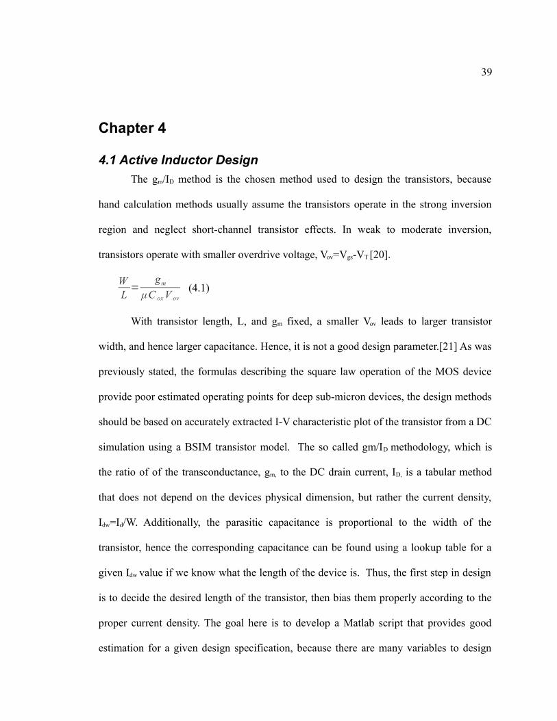
4.1 Active Inductor DesignThe gm/ID method is the chosen method used to design the transistors, because
hand calculation methods usually assume the transistors operate in the strong inversion
region and neglect short-channel transistor effects. In weak to moderate inversion,
transistors operate with smaller overdrive voltage, Vov=Vgs-VT [20].
WL=
gm
μC ox V ov(4.1)
With transistor length, L, and gm fixed, a smaller Vov leads to larger transistor
width, and hence larger capacitance. Hence, it is not a good design parameter.[21] As was
previously stated, the formulas describing the square law operation of the MOS device
provide poor estimated operating points for deep sub-micron devices, the design methods
should be based on accurately extracted I-V characteristic plot of the transistor from a DC
simulation using a BSIM transistor model. The so called gm/ID methodology, which is
the ratio of of the transconductance, gm, to the DC drain current, ID, is a tabular method
that does not depend on the devices physical dimension, but rather the current density,
Idw=Id/W. Additionally, the parasitic capacitance is proportional to the width of the
transistor, hence the corresponding capacitance can be found using a lookup table for a
given Idw value if we know what the length of the device is. Thus, the first step in design
is to decide the desired length of the transistor, then bias them properly according to the
proper current density. The goal here is to develop a Matlab script that provides good
estimation for a given design specification, because there are many variables to design

40
and likely require multiple iterations before arriving at a final design.
For brevity, only the NMOS version of the active inductor is considered in this
example because of its higher transition frequency for the same gm/Id, however, a PMOS
design can be produced in a similar fashion.
For the following example, gm is the small-signal transconductance, go is the small
signal output conductance, given by:
go=ID/VA
where VA is the Early voltage. The transition frequency is defined as ωT and is a “figure of
merit” (FOM) of the switching speed of a transistor. Beyond the transition frequency the
transistor cannot fully charge and discharge its intrinsic capacitance each cycle and,
hence, stops acting like voltage dependent current source. The transition frequency is an
FOM that indicates the quality of the transistor since we want large gm but small width
which means small Cgs. Additionally it is desired for gm to be large while keeping ID small,
for increased energy efficiency.
The gm/ID relationship can be derived as follows:
gm
I D= 1
I D
∂ I D
∂V G=∂ ln I D
∂V G=
∂{ln[ I D
(wL )]}
∂V G
(4.2)
41
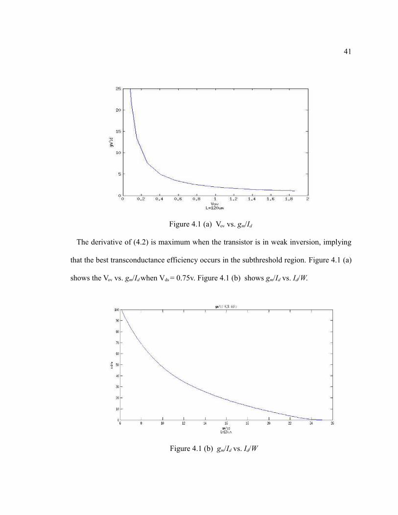
Figure 4.1 (a) Vov vs. gm/Id
The derivative of (4.2) is maximum when the transistor is in weak inversion, implying
that the best transconductance efficiency occurs in the subthreshold region. Figure 4.1 (a)
shows the Vov vs. gm/Id when Vds = 0.75v. Figure 4.1 (b) shows gm/Id vs. Id/W.
Figure 4.1 (b) gm/Id vs. Id/W

42
A lookup table that contains all the necessary small signal parameters is created over a
multiple dimensional space consisting of bias point (e.g., Vgs and Vds) and physical
dimension (e.g., L) of the circuit in figure 4.2 All data for a family of transistors is stored
as data to a file. Such a file can easily be accessed using lookup table techniques using
analytical software (e.g., Matlab).
Figure 4.2 Schematic for creating technology file
The following is a catalog of the lookup functions that were developed for sizing
transistors along with a description of the function. Because the lookup functions
interpolate data from a discrete table, the accuracy of the lookup table depends on the
spacing of the points used to collect the data. A full Matlab script for designing an active
inductor and active VCO using such lookup tables can be found in appendix B.
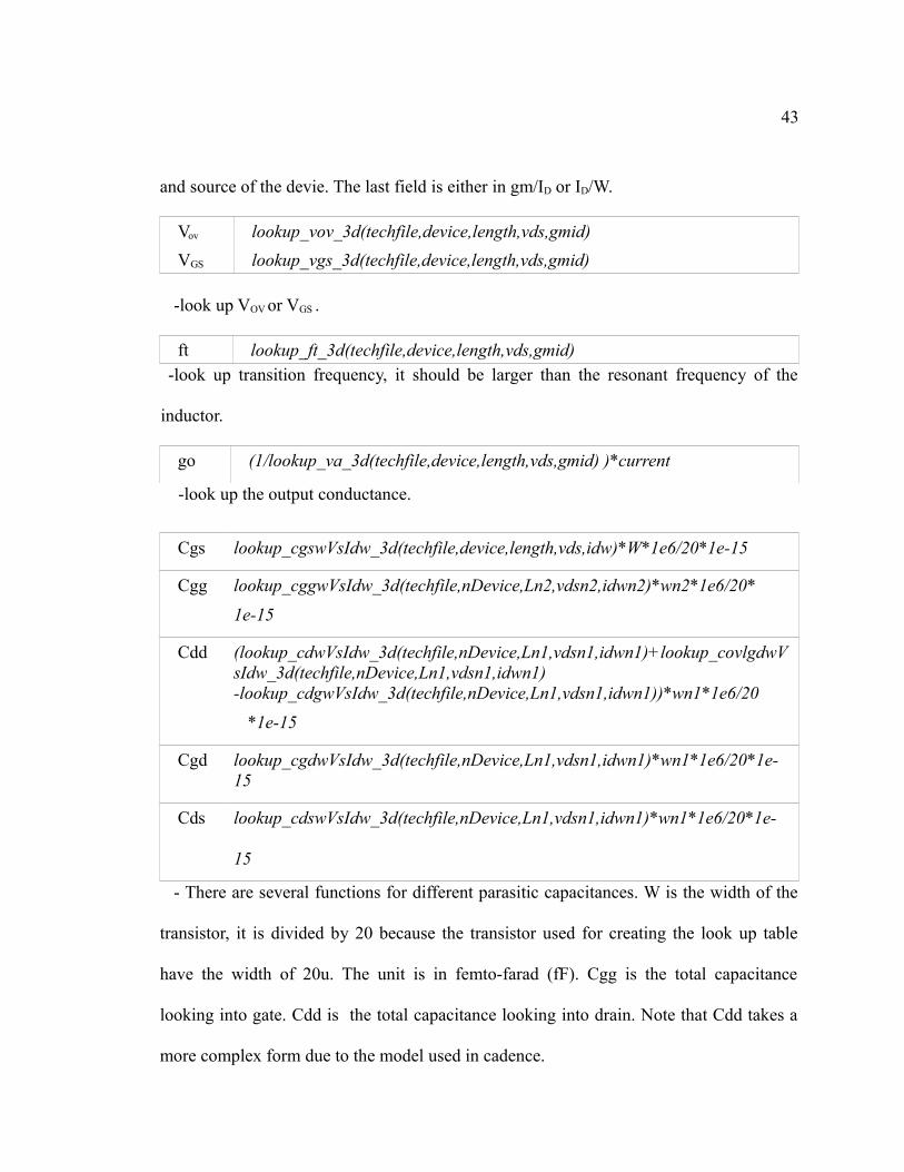
Table 4.1 List of look up functions
gmid lookup_gmid_3d(techfile,device,length,vds,idw)id/w lookup_idw_3d(techfile,device,length,vds,gmid) -look up gmid and id/w. All the lookup functions share the same format. Where
techfile is the path to the lookup table, device is the name of the device, for example,
'pfet' and 'nfet'. length is the length of the transistor in nm. vds is the voltage across drain
+-
+-
43
and source of the devie. The last field is either in gm/ID or ID/W.
Vov lookup_vov_3d(techfile,device,length,vds,gmid)VGS lookup_vgs_3d(techfile,device,length,vds,gmid)
-look up VOV or VGS .
ft lookup_ft_3d(techfile,device,length,vds,gmid) -look up transition frequency, it should be larger than the resonant frequency of the
inductor.
go (1/lookup_va_3d(techfile,device,length,vds,gmid) )*current
-look up the output conductance.
Cgs lookup_cgswVsIdw_3d(techfile,device,length,vds,idw)*W*1e6/20*1e-15
Cgg lookup_cggwVsIdw_3d(techfile,nDevice,Ln2,vdsn2,idwn2)*wn2*1e6/20*1e-15
Cdd (lookup_cdwVsIdw_3d(techfile,nDevice,Ln1,vdsn1,idwn1)+lookup_covlgdwVsIdw_3d(techfile,nDevice,Ln1,vdsn1,idwn1) -lookup_cdgwVsIdw_3d(techfile,nDevice,Ln1,vdsn1,idwn1))*wn1*1e6/20
*1e-15
Cgd lookup_cgdwVsIdw_3d(techfile,nDevice,Ln1,vdsn1,idwn1)*wn1*1e6/20*1e-15
Cds lookup_cdswVsIdw_3d(techfile,nDevice,Ln1,vdsn1,idwn1)*wn1*1e6/20*1e-
15
- There are several functions for different parasitic capacitances. W is the width of the
transistor, it is divided by 20 because the transistor used for creating the look up table
have the width of 20u. The unit is in femto-farad (fF). Cgg is the total capacitance
looking into gate. Cdd is the total capacitance looking into drain. Note that Cdd takes a
more complex form due to the model used in cadence.

44
Figure 4.3 Active inductor
With the gm/ID method, the active inductor can now be designed. The schematic is shown
in Figure 4.3. The supply voltage is set to VDD . Vb2 is chosen to be high enough so it can
turn on M2. It should be reasonable value as it will affect the VDS of M1, as well as the
large signal behavior. The VDS of the transistors can't be determined exactly, so it would
need to be estimated based on previous experience. A good starting point would be
determining the bias currents. Ibias1 is designed to be much larger than ibias2, so set
ibias1 = 10* ibias2. Next, gm/ID of M1 need to be determined. Choosing (gm/ID)1 to be 15.
gm of M1 can be calculated.
>>gm1=gmid1 * (ibias1+ibias2);
To determine the value of VGS1,
>>Vgs1=Lookup_vgs_3d(techfile,nDevice, Ln1, Vdd/2, gmid1);
VDS1 is chosen to be Vdd/2 since the exact value VDS1 cannot be determined beforehand,
but this won't affect the result too much.
(ID/W)1 is found to be
M1
M2
M3
Vb1
Vb2
ibias2
ibias1

45
>> idwn1=Lookup_idw_3d(techfile, nDevice, Ln1, Vdd/2, gmid1);
and the width of the transistor is then
>>wn1=(ibias1+ibias2)/idwn1;
Once, (ID/W)1 is known, width of M1, and all the parasitic capacitance can be
calculated. All the output conductances and their parasitic capacitances can be obtained
by using the function listed in Table 4.1. VDS of M3 is just Vdd-VGS1. Since M3 acts as a
current source and is not changed throughout the design. A fixed width is chosen, and the
(ID/W)3 ratio is obtained.
>> gmid3=lookup_idw_3d(techfile,device,length,vds,idw);
>> Vgs3= Lookup_vgs_3d(techfile,pDevice, Lp3, Vdd-Vgs1, gmid3);
Similarly, all other parameters of M3 are calculated by using the corresponding functions.
The body effect is not taken into account when tabulating the tech file as it adds a lot
more complexity, gmb can be included in gm by multiplying a factor here. The gate to
source voltage of M2 cannot be easily determined since the higher threshold voltage
increase the overdrive voltage for the same gm/ID ratio. Thus, an estimation is used for
VDS2, then relate VDS1 and VDS2 as follows: VDS1 = VGS1-VDS2 .
It is possible to write a while loop to sweep the gm/ID of M2 , for simplicity, a
value of (gm/ID)2 is picked.
>> idwn2=Lookup_idw_3d(techfile, nDevice, Ln1, vdsn2, gmid2);
and the width of the transistor is then
>>wn2=(ibias2)/idwn2;
Once again, the functions from Table 4.1 to are used to compute the output

46
conductance and parasitic capacitances. With all the parameters determined, inductance
value, resonant frequency and quality factor can be calculated by using the equations in
chapter 2.
47
4.2 Active VCO DesignTo use the active inductor in the active VCO, the resonant frequency needs to be
designed at a much higher frequency than the VCO operation frequency. This is due to
large-signal behavior phenomena as explained in the previous chapter. The cross-coupled
pair must provide enough negative resistance cancel out the resistance looking into the
active inductor:
>> R=max(real(Z));
where Z is the impedance of the active inductor and is a function of frequency. The gm of
the cross-coupled pair should be designed to be twice the size of the input resistance, R:
>> gm=(1/R)*2;
The bias current is ibias1, hence gm/ID is then:
>> gm/ID =gm / ibias1
The width, W, can be determined by looking up ID/W:
>> idw=Lookup_idw_3d(techfile, pDevice, Ln1, [], gmid);
>> W = ibias1/idw;
likewise, all the parasitic capacitances and output resistance can be calculated using
similar lookup tables.
Figure 4.4 shows the schematic of the complete design. The parameters and the bias
voltages are given in Table 4.2. Some modifications are made to the current source to
improve its output impedance. Stacked transistors and a pseudo-resistor [22] are used to
increase the output resistance and the resistance of the substrate. The resistance of the
pseudo-resistor is greater than 1MΩ. This configuration improves phase noise because
48
the fluctuation of voltage swing not only affects the DC operating points, but also
changes the junction capacitance. Replica-biasing can also be used [23]. The Active
VCO oscillates at 400MHz. The total power consumed is 55.4μW. Phase noise is
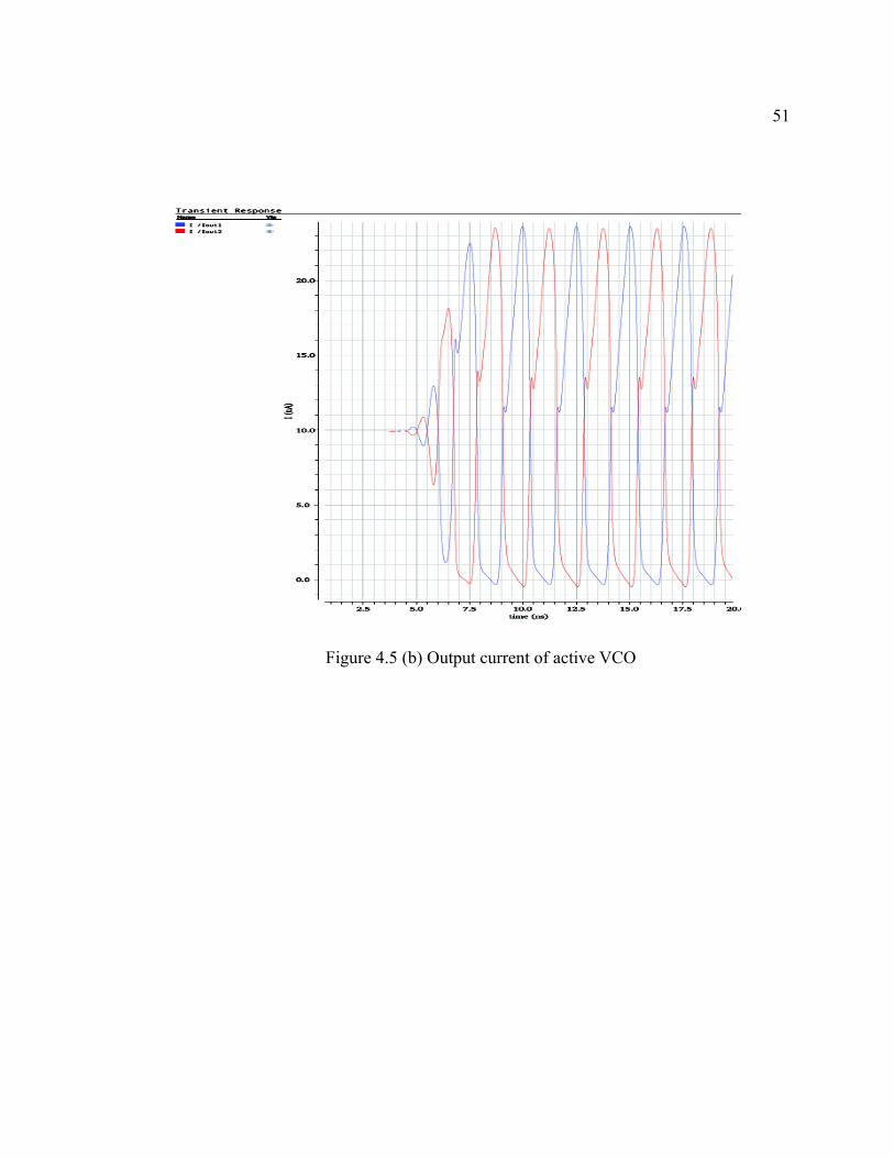
-77dbc/Hz @1MHz offset. Figure 4.5 (a) and (b) show the outputs of the VCO as well as
that of the buffer. The tail transistor spends part of its time operating in the triode region;
thus the tail current does not stay constant. This implies that the drain-to-source voltage
of the NMOS cross-coupled pair can reduce significantly, resulting in a large reduction in
their drain current, as shown in Figure 4.5 (b). This indicates that the Active VCO is
operating in a voltage-limited regime. [19] The use of buffers reduces the overall
frequency due to the additional capacitance, however, they increase the voltage swing.
The reduction in resonant frequency can be compensated by increasing the bias current.
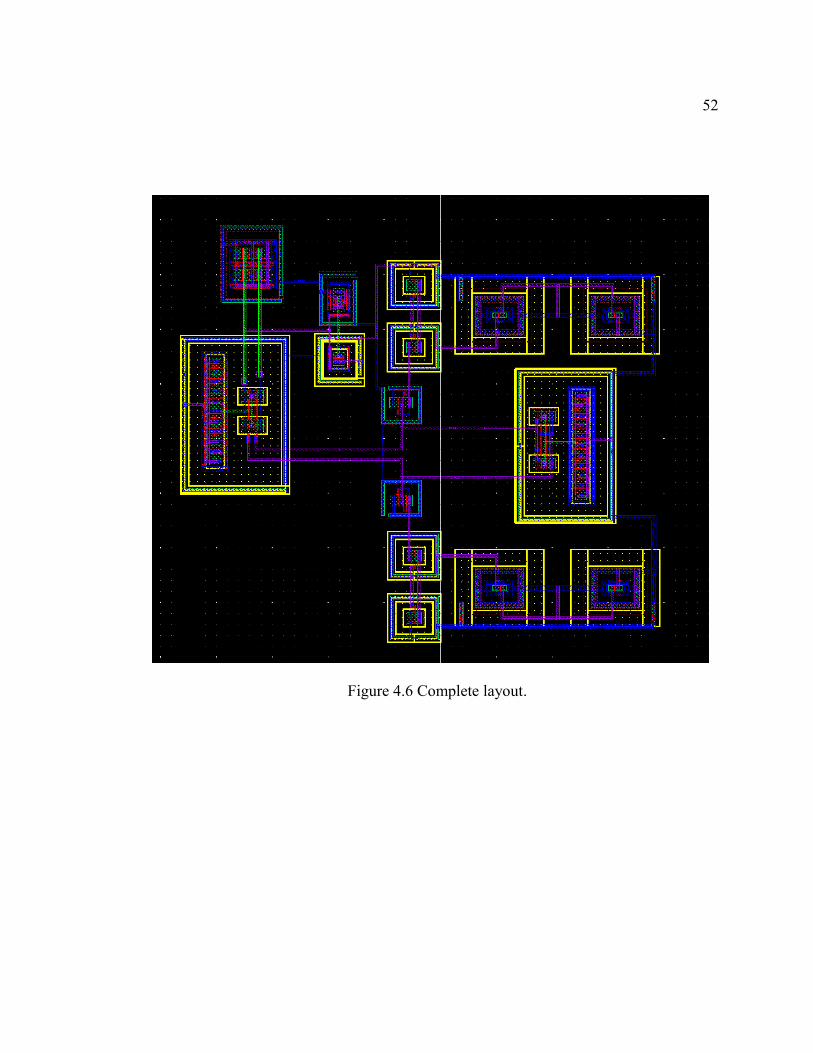
The completed layout is shown in Figure 4.6

49
Figure 4.4 Schematic for Active VCO
1
2
1
2
sub!
sub!
sub!
sub!
sub!
vdd!vdd!
M1
M2
M3
M4
M5
M6
M7
M8
M9 M10
M11
T1 T2
sub!
vdd!vdd!
M12
M13
M14
M15
M16
M17
M18vdd!
sub!
VOUT
Vb1Vb1
Vb2 Vb2
Vb4
Vb3
50
M1 ~M8 T1,T2 M12 ,M14 M17 Vb1 839mVVb2 650mV
M9 , M10
M13,M15
M11,
M16
M16 VDD 1.2V Vb3 810mVVb4 850mV
Table 4.2 Transistors Sizing of Active VCO
Figure 4.5 (a) Output voltage of Active VCO
1u120n
4u240n
1u120n
1μ240n
480n120n
2μ240n
10u480n
51
Figure 4.5 (b) Output current of active VCO
52
Figure 4.6 Complete layout.
53
Chapter 5
5.1 Conclusion and Further WorkThe focus of this thesis is on a structured design approach for gyrator-C active
inductors. A MatlabTM script is developed based on the gm/ID methodology, and a low
power active VCO is designed. The Wu active inductor topology is used for
demonstration, however, with modifications made to the biasing currents, this approach
can be applied to other gyrator-C based active inductors.
The large-signal behavior has been studied and discussed extensively throughout the
thesis and the active VCO is carefully examined. It is shown that the resonant frequency
of the active inductors is reduced under large signal, and such change needs to be
compensated by adjusting the biasing points through many iterations. While active
inductors have considerably more noise than physical inductors, they are useful when
noise isn't the main concern. Furthermore, there are more complicated feedback circuit
that can be employed to reduce noise.
Other possible applications for the active inductors includes using the active inductor as
an RF choke in low-power power amplifier. Because the transient response of the active
inductors are limited by the bandwidth and by power supply future work will be to reduce
the sensitivity to large-signal swings.
54
References[1] A. Thanachayanont and A. Payne. “CMOS floating active inductor and its applications to band-pass filter and oscillator design”. IEE Proceedings, Part G - Circuits, Devices, and Systems, 147(1):42–48, Feb. 2000.
[2] A. Thanachayanont. “A 1.5-V high-Q CMOS active inductor for IF/RF wireless applications”. In Proc. IEEE Asia-Pacific Conf. Circuits Syst., volume 1, pages 654–657,2000.
[3] L. Lu and Y. Liao. “A 4-GHz phase shifter MMIC in 0.18-μmCMOS”. IEEE Microwave and Wireless Components Letters, 15(10):694–696, Oct. 2005.
[4] R.Weng and R. Kuo. “An ωo-Q tunable CMOS active inductor for RF bandpass filters”. In Proc. Int’l Symp. Signals, Systems, and Electronics, pages 571–574, Aug. 2007.
[5] A. Tang, F. Yuan, and E. Law. “A new CMOS active transformer QPSK modulator with optimal bandwidth control”. IEEE Trans. on Circuits Syst. II., 55(1):11–15, Jan. 2008.
[6] A. Tang, F. Yuan, and E. Law. “CMOS class AB active transformers with applications in LC oscillators”. In IEEE Int’l Symp. Signals, Systems and Electronics, pages 501–504,Montreal, Aug. 2007.
[7]F. Yuan, CMOS Acitve Inductors and Transformers:Principle, Implementation, and Applications, Springer, 2008.
[8]F. Yuan, “CMOS active Transformers” , Circuits, Device &Systems, IET, vol.1, pp 494-508, Dec. 2007.
[9]Y.Wu, Xi.Ding, M.smail,”Rf bandpass filter design based on cmos active inductors” ieee transactions on circuits and systems—ii: analog and digital signal processing, vol. 50, no. 12, december 2003
[10]Y. Wu, el al “A novel cmos fully differential inductorless rf bandpass filter” ISCAS 2000 - IEEE International Symposium on Circuits and Systems, May 28-31, 2000
[11] C. Andriesei and L. Goras, “On the Tuning Possibilities of an RF Bandpass Filter with Simulated Inductor”, International Semiconductor Conference, CAS 2007, vol. 2,
55
pp. 489–492, 2007, October 2007,Romania
[12] C. Andriesei and L. Goras, “ Negative Resistance Based Tuning of an RF bandpass Filter” Circuits and Systems for Communications, 2008.
[13]A. Abidi, “Noise in active resonators and the available dynamic range,” IEEE Trans. Circuits Syst.-I, vol. 39, pp. 296–299, Apr. 1992.
[14]G. Gonzalez, Foundations of Oscillator Circuit Design , Artech House Publishers, Dec 2006.
[15]Y. Zhou “A comparative study of lock Range of Injuection-Locked Acitve Inductor Osillators. Circuits and Systems (MWSCAS),Aug. 2010.
[16]A. Tang A F. Yuan A E. Law. A new constant-Q CMOS active inductor with applications to low-noise oscillators, Oct, 2008
[17]R. Lee Bunch,Large signal analysis of MOS varactors in CMOS -Gm LC VCOs, IEEE JOURNAL OF SOLID-STATE CIRCUITS, VOL. 38, NO. 8, AUGUST 2003
[18]C.C.Enz, F.Krumenacher, and E.A.Vittoz,” A Basic Property of MOSTransistor model valid in all regions of operation amd dedicated to low-voltageand low-current applications”, Analog Integrated Circuits Signal Process.,Vol.8, pp83-114,1995
[19]Design Issues in CMOS Differential LC OscillatorsIEEE JOURNAL OF SOLID-STATE CIRCUITS, VOL. 34, NO. 5, MAY 1999
[20]gm/ID based methodology for the design of CMOS analog circuits and its application to the synthesis of a silicon-ion- insulator micropower OTA. IEEE Journal of Solid State Circuits. Vol. 31, pp 1314-1319, Sept. 1996.
[21]D. Flandre, A. Viviani, J.-P. Eggermont, P. Jespers,"Improved synthesis of regulated-cascode gain-boosting CMOS stage using symbolic analysis and gm/ID methodology", IEEE Journal of Solid-State Circuits (SpecialIssue on 22nd ESSCIRC conference), 32 (1997) 1006-1012.
[22]M.-T. Shiue, K.-W. Yao and C.-S.A. Gong. “Tunable high resistance voltage-controlled pseudo-resistor with wide input voltage swing capability” Electronics Letters .vol 47 , Issue: 6 pp 377 - 378 March 17 2011
56
[23] D. DiClemente and F. Yuan. “Current-mode phase-locked loops : a new architecture”. IEEE Trans. on Circuits Syst. II., 54(4):303–307, Apr. 2007.
[24] A. Abidi, “Noise in active resonators and the available dynamic range,”IEEE Trans. Circuits Syst.-I, vol. 39, pp. 296–299, Apr. 1992.
[25]Kuhn, W.B. , “Dynamic range of high-Q OTA-C and enhanced-Q LC RFbandpass filters,” in Proc. IEEE Midwest Circuits Systems, 1995, pp.767–771.
[26]Thomas H. Lee,Oscillator Phase Noise: A Tutorial IEEE JOURNAL OF SOLID-STATE CIRCUITS, VOL. 35, NO. 3, MARCH 2000
[27] B. Razavi. Design of analog CMOS integrated circuits. McGraw-Hill, Boston, 2001.

57
Appendix A:The Derivation of equations 2.2~2.5

58
A more complex model used in simulation, including the cross-coupled pairs. (-gm and its parasitic capacitance)
after some rearranging the term, and put into the form given for ZIN , we get ZIN =
59
Function “Matlab(x)” is used to to export Zin into matlab.
60
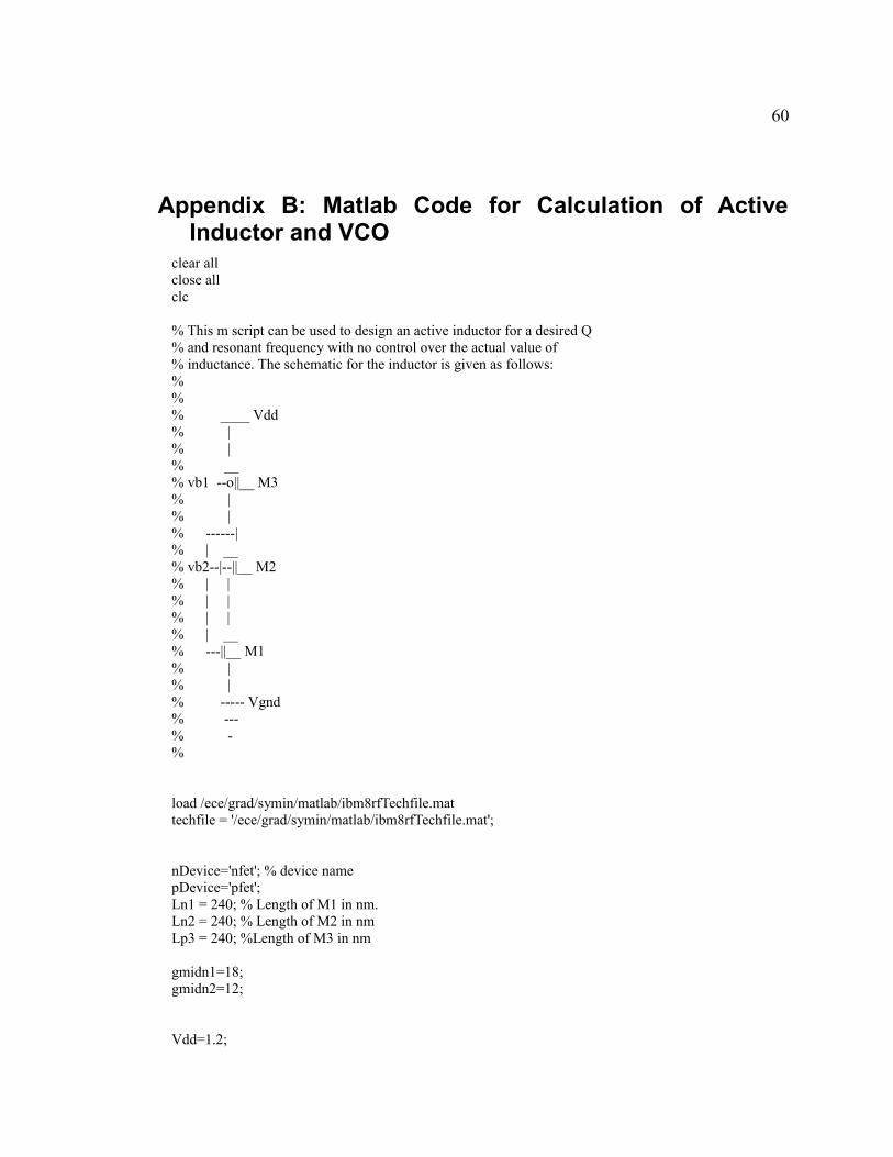
Appendix B: Matlab Code for Calculation of Active Inductor and VCO
clear allclose allclc
% This m script can be used to design an active inductor for a desired Q% and resonant frequency with no control over the actual value of% inductance. The schematic for the inductor is given as follows:%% % ____ Vdd% |% |% __% vb1 --o||__ M3% | % |% ------|% | __% vb2--|--||__ M2% | |% | |% | |% | __% ---||__ M1% |% |% ----- Vgnd% ---% -%
load /ece/grad/symin/matlab/ibm8rfTechfile.mattechfile = '/ece/grad/symin/matlab/ibm8rfTechfile.mat';
nDevice='nfet'; % device namepDevice='pfet';Ln1 = 240; % Length of M1 in nm. Ln2 = 240; % Length of M2 in nmLp3 = 240; %Length of M3 in nm
gmidn1=18;gmidn2=12;
Vdd=1.2;
61
vdsp3=800e-3; %vds of M3Vgs1=lookup_vgs_3d(techfile,nDevice,Ln1,Vdd-vdsp3-.1,gmidn1);
Vgs2=lookup_vgs_3d(techfile,nDevice,Ln2,0.3,gmidn2);
Vb2=600e-3vdsn2=Vgs1-(Vb2-Vgs2);%vds of M2vdsn1=Vdd-vdsp3-vdsn2;
Resfreq=3e9; %desired resonant frequncy
ibias1 = 11e-6;%10e-6; %Desired additional bias current through transistor M1ibias2 = 1.0e-6; % Desired bias current through transistor M2
idwn1 =lookup_idw_3d(techfile,nDevice,Ln1,vdsn1,gmidn1)wn1=(ibias1+ibias2)/idwn1fT = lookup_ft_3d(techfile,nDevice,Ln1,vdsn1,gmidn1)
gm1=gmidn1*(ibias1+ibias2);go1=(1/lookup_va_3d(techfile,nDevice,Ln1,vdsn1,gmidn1))*(ibias1+ibias2);
Cgs1=-lookup_cgswVsIdw_3d(techfile,nDevice,Ln1,vdsn1,idwn1)*wn1*1e6/20*1e-15 Cdg1=lookup_cdwVsIdw_3d(techfile,nDevice,Ln1,vdsn1,idwn1)*wn1*1e6/20*1e-15 ... +lookup_covlgdwVsIdw_3d(techfile,nDevice,Ln1,vdsn1,idwn1)*wn1*1e6/20*1e-15 ... -lookup_cdgwVsIdw_3d(techfile,nDevice,Ln1,vdsn1,idwn1)*wn1*1e6/20*1e-15 ;Cgd1=-lookup_cgdwVsIdw_3d(techfile,nDevice,Ln1,vdsn1,idwn1)*wn1*1e6/20*1e-15;Cds1=lookup_cdswVsIdw_3d(techfile,nDevice,Ln1,vdsn1,idwn1)*wn1*1e6/20*1e-15;
idwn2 = lookup_idw_3d(techfile,nDevice,Ln2,vdsn2,gmidn2)wn2=(ibias2)/idwn2fT = lookup_ft_3d(techfile,nDevice,Ln2,vdsn2,gmidn2)
gm2=gmidn2*(ibias2)*1.2go2=(1/lookup_va_3d(techfile,nDevice,Ln2,vdsn2,gmidn2))*(ibias2)
Cgs2=lookup_cggwVsIdw_3d(techfile,nDevice,Ln2,vdsn2,idwn2)*wn2*1e6/20*1e-15;Cdg2=lookup_cdwVsIdw_3d(techfile,nDevice,Ln2,vdsn2,idwn2)*wn2*1e6/20*1e-15+ ... lookup_covlgdwVsIdw_3d(techfile,nDevice,Ln2,vdsn2,idwn2)*wn2*1e6/20*1e-15... -lookup_cdgwVsIdw_3d(techfile,nDevice,Ln2,vdsn2,idwn2)*wn2*1e6/20*1e-15; Cds2=lookup_cdswVsIdw_3d(techfile,nDevice,Ln2,vdsn2,idwn2)*wn2*1e6/20*1e-15 ;
wp3=1e-6;
gmid3= 19.7/1.1; %lookup_gmid_3d(techfile,pDevice, Lp3, ,vdsp3)idwp3 =lookup_idw_3d(techfile,nDevice,Lp3,vdsp3,gmid3);

62
go3=(1/lookup_va_3d(techfile,pDevice,Lp3,vdsp3,gmid3))*(ibias2);
Cdd3=lookup_cdwVsIdw_3d(techfile,pDevice,Lp3,vdsp3,idwp3)*wp3*1e6/20*1e-15 ... +lookup_covlgdwVsIdw_3d(techfile,pDevice,Lp3,vdsp3,idwp3)*wp3*1e6/20*1e-15 ...-lookup_cdgwVsIdw_3d(techfile,pDevice,Lp3,vdsp3,idwp3)*wp3*1e6/20*1e-15;
f=[1:1e6:10e9+1]';s=2*pi*i*f;
% Zin of active inductorz=((Cgs1 + Cgd1 + Cdg2 + Cdd3) / (Cgs1 * Cgs2 + Cdg1 * Cgs1+ Cds1 * Cgs1 + Cdd3 * Cgs2 + Cdg2
* Cgs2 + Cgd1 * Cgs2 + Cds1* ...Cgd1 + Cds1 * Cdd3 + Cdg1 * Cdg2 + Cds1 * Cdg2 + Cdg1 * Cdd3)* s + (go2 + go3) / (Cgs1 * Cgs2 +
Cdg1 * Cgs1 + Cds1 * Cgs1 + ...Cdd3 * Cgs2 + Cdg2 * Cgs2 + Cgd1 * Cgs2 + Cds1 * Cgd1 + Cds1 *Cdd3 + Cdg1 * Cdg2 + Cds1 *
Cdg2 + Cdg1 * Cdd3)) ./ (s .^ 2 + ...(gm2 * Cgs1 + go1 * Cgs1 + go2 * Cgs1 + go2 * Cgs2 + Cgd1 * gm1+ Cgd1 * gm2 - Cdg1 * gm2 +
Cdg2 * gm2 + Cdd3 * gm2 + Cdd3 * ...go1 + Cdg2 * go1 + Cgd1 * go1 + Cds1 * go2 + Cdd3 * go2 + Cdg2* go2 + go3 * Cgs2 + Cdg1 * go3 +
Cds1 * go3) / (Cgs1 * Cgs2 ...+Cdg1 * Cgs1 + Cds1 * Cgs1 + Cdd3 * Cgs2 + Cdg2 * Cgs2 + Cgd1 *Cgs2 + Cds1 * Cgd1 + Cds1 *
Cdd3 + Cdg1 * Cdg2 + Cds1 * Cdg2 ...+Cdg1 * Cdd3) * s + (gm1 * gm2 + gm1 * go2 + go1 * go2 + go3 *gm2 + go3 * go1 + go3 * go2) /
(Cgs1 * Cgs2 + Cdg1 * Cgs1 + ...Cds1 * Cgs1 + Cdd3 * Cgs2 + Cdg2 * Cgs2 + Cgd1 * Cgs2 + Cds1 *Cgd1 + Cds1 * Cdd3 + Cdg1 *
Cdg2 + Cds1 * Cdg2 + Cdg1 * Cdd3)); ...
w01=(gm1 * gm2 + gm1 * go2 + go1 * go2 + go3 *gm2 + go3 * go1 + go3 * go2) / ((Cgs1 * Cgs2 + Cdg1 * Cgs1 +Cds1 * Cgs1 + Cdd3...
* Cgs2 + Cdg2 * Cgs2 + Cgd1 * Cgs2 + Cds1 *Cgd1 + Cds1 * Cdd3 + Cdg1 * Cdg2 + Cds1 * Cdg2 + Cdg1 * Cdd3));
resfreq1=sqrt(w01)/(2*pi)
figure;
subplot(211)hold on
plot(f,real(z),'black');plot(f,imag(z),'-.black');legend('real','imag');
subplot(212)plot(f,imag(z)./(2*pi*f),'r');
hold off
indc=imag(z(1,1)./(2*pi*1)) %%---------------------------------------------------------------------------------------------------------
63
%active VCO
Lp=240vdsp=500e-3
R=10e3%max(real(z))gm=1/R*2id=5e-6;
gmid=gm/id idw = lookup_idw_3d(techfile,pDevice,Lp,[],gmid)fT = lookup_ft_3d(techfile,pDevice,Lp,[],gmid)w=id/idw Cgs=lookup_cggwVsIdw_3d(techfile,pDevice,Lp,vdsp,idw)*w*1e6/20*1e-15Cdg=lookup_cdwVsIdw_3d(techfile,pDevice,Lp,vdsp,idw)*w*1e6/20*1e-15go=(1/lookup_va_3d(techfile,pDevice,Lp,vdsp,gmid))*(10e-6)
Cx=(Cdg+2*Cgs);Cds=0.5e-15%lookup_cdsw_3d(techfile,pDevice,Lp,vdsp,idw)*w*1e6/20*1e-15
z3 = ((Cgs1 + Cgd1 + Cdg2 + Cdd3) / (Cgs1 * Cgs2 + Cx *Cgs1 + Cdg1 * ...Cgs1 + Cds1 * Cgs1 + Cds * Cgs1 + Cdg2 * Cgs2 +Cgd1 * Cgs2 + Cdd3 * Cgs2 ...+ Cds1 * Cgd1 + Cx * Cgd1 +Cx * Cdd3 + Cx * Cdg2 + Cds * ...Cdd3 + Cdg1 * Cdg2 + Cdg1 *Cdd3 + Cds * Cgd1 + Cds * Cdg2 + Cds1 * Cdg2 + ...Cds1 * Cdd3) * s+ (go2 + go3) / (Cgs1 * Cgs2 + Cx * Cgs1 + Cdg1 * Cgs1 ...+Cds1 * Cgs1 + Cds * Cgs1 + Cdg2 * Cgs2 + Cgd1 * Cgs2 + Cdd3 *Cgs2 + Cds1 * ...Cgd1 + Cx * Cgd1 + Cx * Cdd3 + Cx* Cdg2 + Cds * Cdd3 + Cdg1 * ...Cdg2 + Cdg1 * Cdd3 + Cds * Cgd1 +Cds * Cdg2 + Cds1 * Cdg2 + Cds1 * Cdd3)) ./ ...(s .^ 2 + (gm2 * Cgs1+ go1 * Cgs1 + go2 * Cgs1 + go2 * Cgs2 + Cgd1 * gm1 + Cdg2 ...*gm2 + Cgd1 * gm2 - Cdg1 * gm2 + Cdd3 * gm2 + Cdg2 * go1 + Cgd1* go1 + Cdd3 * go1 ...+ Cdd3 * go2 + Cx * go2 + Cds1 * go2 +Cdg2 * go2 + Cds * go2 - gm * Cgs1 + ...go * Cgs1 + go3 * Cgs2 +Cds1 * go3 + Cx * go3 - gm * Cdd3 - gm * Cdg2 + Cdg1 ...* go3+ Cds * go3 - gm * Cgd1 + go * Cgd1 + go * Cdg2 + go * Cdd3) /(Cgs1 * Cgs2 ...+ Cx * Cgs1 + Cdg1 * Cgs1 + Cds1 * Cgs1 + Cds* Cgs1 + Cdg2 * Cgs2 + Cgd1 * ...Cgs2 + Cdd3 * Cgs2 + Cds1 * Cgd1+ Cx * Cgd1 + Cx * Cdd3 + Cx * Cdg2 ...+ Cds * Cdd3+ Cdg1 * Cdg2 + Cdg1 * Cdd3 + Cds * Cgd1 + Cds * Cdg2 + Cds1 *Cdg2 + ...Cds1 * Cdd3) * s + (gm1 * gm2 + gm1 * go2 + go1 * go2 +go3 * gm2 + go3 * go1 + go3 ...* go2 - gm * go2 + go * go2 - gm *go3 + go * go3) / (Cgs1 * Cgs2 + Cx * Cgs1 + ...Cdg1 * Cgs1 +Cds1 * Cgs1 + Cds * Cgs1 + Cdg2 * Cgs2 + Cgd1 * Cgs2 + Cdd3 *Cgs2 + Cds1 ...* Cgd1 + Cx * Cgd1 + Cx * Cdd3 + Cx* Cdg2 + Cds * Cdd3 + Cdg1 * Cdg2 ...• Cdg1 * Cdd3 + Cds * Cgd1 +Cds * Cdg2 + Cds1 * Cdg2 + Cds1 * Cdd3)); ...•
w3=(gm1 * gm2 + gm1 * go2 + go1 * go2 +go3 * gm2 + go3 * go1 + go3 * go2 - gm * go2 + go * ...go2 - gm *go3 + go * go3) / (Cgs1 * Cgs2 + Cx * Cgs1 + Cdg1 * Cgs1 +Cds1 * Cgs1 + Cds ...* Cgs1 + Cdg2 * Cgs2 + Cgd1 * Cgs2 + Cdd3 *Cgs2 + Cds1 * Cgd1 + Cx * Cgd1 +Cx * ...Cdd3 + Cx* Cdg2 + Cds * Cdd3 + Cdg1 * Cdg2 + Cdg1 * Cdd3 + Cds * Cgd1 +Cds * Cdg2 + ...Cds1 * Cdg2 + Cds1 * Cdd3);

64
resfreq3=sqrt(w3)/(2*pi)