
Simulations of charge carrier transport in disordered organic polymers
on June 26, 2018http://rsta.royalsocietypublishing.org/Downloaded from
The study of charge transport through organicthin films: mechanism, tools and applications
BY EMILY A. WEISS1, JENNAH K. KRIEBEL
1, MARIA-ANITA RAMPI2
AND GEORGE M. WHITESIDES1,*
1Department of Chemistry and Chemical Biology, Harvard University,12 Oxford Street, Cambridge, MA 02138, USA
2Dipartimento di Chimica, Universita Di Ferrara, 44100 Ferrara, Italy
In this paper, we discuss the current state of organic and molecular-scale electronics,some experimental methods used to characterize charge transport through molecularjunctions and some theoretical models (superexchange and barrier tunnelling models)used to explain experimental results. Junctions incorporating self-assembled monolayersof organic molecules—and, in particular, junctions with mercury-drop electrodes—aredescribed in detail, as are the issues of irreproducibility associated with such junctions(due, in part, to defects at the metal–molecule interface).
Keywords: self-assembled monolayer; alkanethiolates; superexchange;molecular junctions; defects
Onelec
*A
1. Introduction. Organic and molecular-scale electronics: the drivetowards miniaturization, versatility and low-cost device fabrication
This paper describes some of the theoretical models and experimental tools usedto characterize charge transport (CT) through films of organic molecules andpolymers. The emergence of nanotechnology from fundamental science has beenmarked, in part, by the birth of the distinct fields of molecular-scale electronicsand organic electronics (sometimes called ‘molecular materials for electronics’;Jortner & Ratner 1997) from the field of molecular conduction, which originatedwith studies of charge transfer complexes in the 1940s. A molecular-scale elec-tronic device—the first of which, a molecular diode, was proposed by Aviram &Ratner (1974)—is one in which a single molecule performs an electronic function(or an array of molecules performs the function in parallel). Organic electronics(Farchioni & Grosso 2001; Malliaras 2003; Facchetti et al. 2005)—a field thatoriginated with the discovery by Heeger, MacDiarmid and Shirakawa ofelectrical conduction in doped organic polymers (Chiang et al. 1977)—is theuse of films of molecules and polymers as the semiconducting (chargetransporting) materials, electrodes or dielectric materials within electronicdevices such as light emitting diodes (Hutchison et al. 1999; Morteani 2003;
Phil. Trans. R. Soc. A (2007) 365, 1509–1537
doi:10.1098/rsta.2007.2029
Published online 12 April 2007
e contribution of 12 to a Discussion Meeting Issue ‘Supramolecular nanotechnology for organictronics’.
uthor for correspondence ([email protected]).
1509 This journal is q 2007 The Royal Society

E. A. Weiss et al.1510
on June 26, 2018http://rsta.royalsocietypublishing.org/Downloaded from
Tseng et al. 2006), field effect transistors (Kudo & Yamashina 1984;Dimitrakopoulos & Mascaro 2001; Dimitrakopoulos & Malenfant 2002; Newmanet al. 2004; Shankar & Jackson 2004; Panzer et al. 2005) and solar cells (Gregg2003; Gledhill et al. 2005; Shaheen et al. 2005).
In general, efforts to incorporate molecules and polymers into electronic deviceshave been motivated by six major considerations (Cahen & Hodes 2002; Vilan &Cahen 2002a): (i) molecules (1–2 nm) are smaller than the smallest features insemiconductors (presently approximately 90 nm; with well-defined engineeringdevelopment, less than 20 nm) and might therefore facilitate the packing of morecomputational power onto a smaller footprint, (ii) the electronic properties ofmolecules and polymers are tunable by organic synthesis; these procedures can, inprinciple, have very low cost, (iii) under certain conditions, molecules self-assembleintoorderedmonolayers (SAMs) andmultilayers on surfaces, and into orderedarraysin solution, (iv) films of molecules and polymers can be deposited over large areas onflexible substrates, (v) the electronic and optical properties ofmanymolecules can becontrolled via modulation of temperature, electric and magnetic fields and otherenvironmental parameters, and (vi) assemblies of molecules perform complex, high-efficiency electronic and optoelectronic charge and energy transport functions innature (e.g. electron transport, photosynthesis, coupling of one- and two-electronprocesses in metabolism).
Molecular-scale electronics is, so far, a purely academic pursuit suffering frompoor reproducibility among measurements of the same systems gathered usingdifferent techniques, a set of daunting experimental issues concerning theconnection of fragile molecules to macroscopic leads, and an incompletetheoretical basis. Furthermore, this field now suffers from both a well-deservedlack of credibility (Service 2003) and an identity crisis: ‘Is the point of molecular-scale electronics to gain a detailed mechanistic understanding of CT throughmolecules or to build functional devices?’ The performance of systems suited toevaluate the electrical properties of individual molecules—for instance, breakjunctions and scanning tunnelling microscopy experiments under ultra high-vacuum conditions and low temperatures—does not easily translate to theperformance of practical devices. In the immediate future, organic electronicdevices (Malliaras & Friend 2005) are anticipated to find a place in commercialmarkets where mechanical flexibility, low cost, chemical sensitivity, opticalproperties and large-area applicability are valued over high performance,markets such as transaction cards, identification tags and large-area displays.
Potential applications aside, the fundamental studies of CT through organicmolecules—especially at the interfaces between organics and metals orsemiconductors—that define the field of molecular-scale electronics today arenecessary for continued innovation in organic electronics. Self-assembledmonolayers (SAMs) are an important tool in creating metal/semiconductor–molecule junctions that can be characterized electrically using a variety ofinstrumentation. In the following sections, we will discuss mechanisms of CTapplicable to both molecular-scale and organic electronic devices, and give aqualitative description of non-resonant superexchange tunnelling, the widelyaccepted mechanism for the transport of charge over long distances in moleculesin the solution phase, and a very useful framework to describe CT through SAMsof organic molecules. We will then describe some of the tools used to study CTthrough SAMs—in particular, the mercury-drop junction—and issues of
Phil. Trans. R. Soc. A (2007)

1511Charge transport through organic films
on June 26, 2018http://rsta.royalsocietypublishing.org/Downloaded from
reproducibility of experiments using these techniques. Finally, we will give someconcluding remarks and discuss future directions for the fields of molecular-scaleand organic electronics.
2. Mechanisms of charge transport through organic films
The rate of long-distance (greater than 1 nm) CT is dictated by somecombination of a strongly distance-dependent tunnelling mechanism and weaklydistance-dependent incoherent transport (Jortner 1976; Marcus & Sutin 1986).The contributions of each of these mechanisms to CT through a metal–insulator–metal (MIM) junction or an organic film are dictated by the energy gap betweenthe work function or energy band of the electrode that injects the charge carrier(electron or hole) and the energy of the orbitals of the insulating organicmaterial. When this energy gap is on the order of kbT, molecular orbitals areenergetically accessible to the incoming charge carrier and a short-livedoxidation or reduction of the molecule or polymer occurs. In a molecularjunction, this charge is then absorbed by the other electrode; in an organic film, ithops to another molecule until it reaches an interface with a collecting electrodeor recombines with a complementary charge carrier. The type of CT thatproceeds via real intermediate states that couple to internal nuclear motions ofthe bridge and the surrounding medium is called incoherent or sequential CT(Davis et al. 1998; Nitzan 2001; Berlin et al. 2002).
For MIM junctions where the work functions of the electrodes lie well withinthe energy gap between the highest occupied and lowest unoccupied molecularorbitals (the HOMO–LUMO gap) of the insulating material, CT proceeds by anon-resonant tunnelling process. The difference between tunnelling and realcharge injection is the time the charge carrier spends in the organic layer. If thestate in which the molecule is oxidized or reduced (the state in which the chargecarrier resides on the bridge) is energetically unfavourable, then the time forwhich this state exists is vanishingly small, and is given by the Land-auer/Buttiker contact time, tLB (Nitzan et al. 2000). In the limit of largeenergy gap for injection, EG, this time is of the simple uncertainty principle form
tLBzNZ
EG
; ð2:1Þ
where N is the number of, bridge sites. For alkane wires, tLB is sub-femtosecond. This time is a great deal shorter than the period, 2p/ul, of theenvironmental vibrations or polarizations (where the vibrational mode isdesignated l) that localize charge. In this limit, then, the mechanism should becoherent tunnelling, where the only vibronic coupling is the very weak inelasticelectron tunnelling signal (IETS) from intermediate (virtual) state nuclearreorganization (Wang et al. 2003a; Galperin et al. 2004; Kushmerick et al.2004; Seminario & Cordova 2004; Selzer et al. 2004a; Troisi & Ratner 2004;Wang et al. 2004a,b, 2005).
When EGwkBT (e.g. oligophenylenevinylene wires; Kubatkin et al. 2003), theLandauer formula fails because charges localize on the wire and move by apolaron-type mechanism (Segal et al. 2000, 2003; through vibronic coupling tothe l mode) that does not conform to the elastic-scattering limit assumed by
Phil. Trans. R. Soc. A (2007)
E. A. Weiss et al.1512
on June 26, 2018http://rsta.royalsocietypublishing.org/Downloaded from
Landauer. In that case, far more general non-equilibrium Green’s functiontechniques (Wingreen et al. 1993; Datta 1995, 2005; Damle et al. 2002; Xue et al.2002; Seideman & Guo 2003) and other hopping models (Berlin & Ratner 2005)have been useful to characterize transport through junctions and films ofmolecules or polymers. We will discuss both tunnelling and hopping mechanismsin this section.
(a ) Non-resonant coherent superexchange tunnelling
The calculation of the coherent, elastic conductance, g, across a moleculesandwiched between two continuous densities of states, and in the presence of atime-dependent voltage, is most often approached through the Landauer formula(Datta 1995,2001, 2005; Emberly & Kirczenow 2000; Seideman & Guo 2003;Troisi & Ratner 2003),
g Z2e2
h
X
i
Ti; ð2:2Þ
whereT is the scatteringmatrix, whose elements give the probability of scattering ofthe electron in channel i, and 2e2/hZ(12.8 kU)K1 is the quantum of conductance.The scattering matrix can be expanded in Green’s function of the molecule (Liuet al. 2005) or estimated via superexchange formulation, as described below.
The form of the scattering matrix directly reflects the mechanism by which thecharge moves through the junction, and there are two such mechanisms. The firstis direct tunnelling, which takes place only if the wave functions of the twoelectrodes extend far enough into the junction to overlap such that they aredirectly electronically coupled. The second mechanism of non-resonant CT inmolecular junctions (which almost always applies if we are, indeed, speaking ofmolecular conduction and not just chemical modification of a metal surface) issuperexchange: superexchange is an indirect transfer of electrons or holes fromdonor to acceptor through an energetically well-isolated bridge, during whichbridge orbitals are utilized solely as a coupling medium (Kramers 1934;Anderson 1950, 1959). The term superexchange was first used to describe theindirect exchange coupling of unpaired magnetic spins via orbitals having pairedspins; diamagnetic orbitals acquire paramagnetic character through mixing withcharge transfer excited state configurations. Superexchange is thought to be animportant mechanism for efficient electron transfer within the photosyntheticreaction centre (Marcus 1987; Ogrodnik & Michel-Beyerle 1989) and has beenstudied in various biomimetic systems (Kilsa et al. 2001; Lukas et al. 2002).
In CT that occurs via superexchange, the charge carrier (either an electron ora hole) does not remain on the bridge long enough to experience dephasing bynuclear motions of the bridge (hence the nomenclature ‘coherent super-exchange’). The time spent in the states—‘virtual excitations’—that themolecule occupies between the instance the electron leaves the donor andwhen it arrives at the acceptor is inversely proportional to the energy gapbetween the electronically coupled orbitals (equation (2.1)).
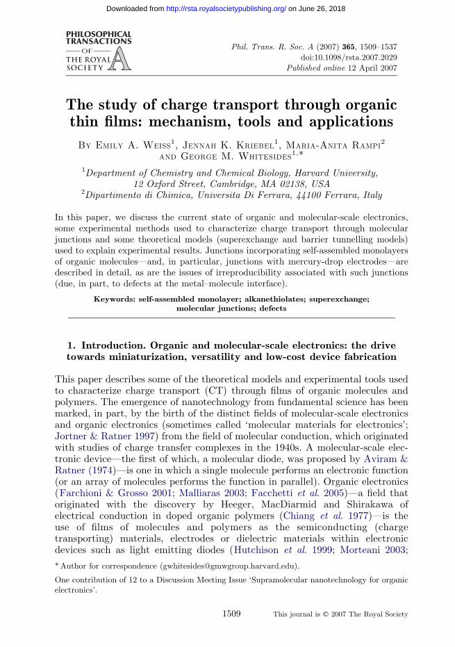
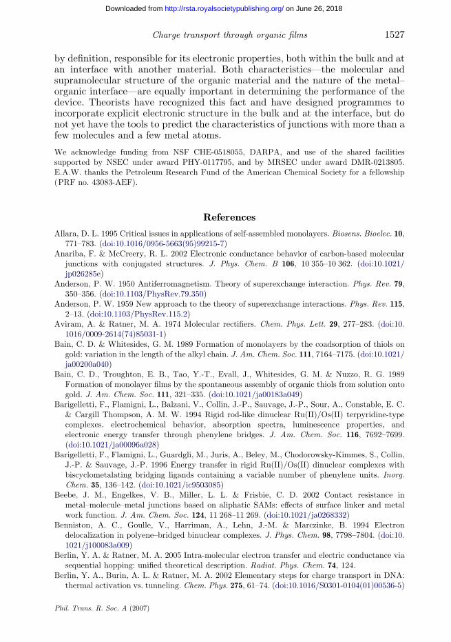
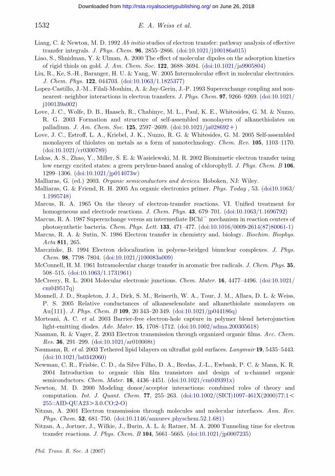
Figure 1a,b are schematics of the simplest cases of both electron and holesuperexchange processes, where a single molecular orbital (either the LUMO inthe case of electron conduction or the HOMO in the case of hole conduction) actsas the conduit for the charge carrier between electrodes 1 and 2. We will discuss
Phil. Trans. R. Soc. A (2007)
molecular LUMO
1 2
+
A2 A3
+
A1
molecularLUMO
1 2
molecularLUMO
1 2
–
+ +
–
A1>> A2= A3
(i)(a)
molecularLUMO
molecularLUMO
A1B3
+
A1B1
molecular LUMO
1
2
1
2
1
2
A1B2
++
+
––
B3> B1>> B2
(ii)
molecularLUMO
molecularLUMO
molecular LUMO
A1B3C1
1
2
++
–
A1B3C2
1
2
+
A1B3C3
1
2
+–
C3> C1, C2
(iii)
Figure 1. Diagrams of (a) electron and (b) hole multistep superexchange tunnelling processeswithin a metal–molecule–metal junction where all conduction takes place through either the (a)LUMO or (b) HOMO of the molecule. The shaded areas indicate occupied states of the metalelectrodes and the arrows are electrons. The system is a statistical mixture of the configurations(where each diagram is a configuration), and the probability of the system being in a specificconfiguration is given by the letters below each diagram. The progression of both electron and holesuperexchange is: A1/B3/C3, with a total probability of A1B3C3. (a) Electron conduction:(i) zero bias, (ii) step 1, electron injection, and (iii) step 2, electron absorption. (b) Hole conduction:(i) zero bias, (ii) step 1, hole injection, and (iii) step 2, hole absorption.
1513Charge transport through organic films
Phil. Trans. R. Soc. A (2007)
on June 26, 2018http://rsta.royalsocietypublishing.org/Downloaded from

molecularHOMO
1 2 molecularHOMO
1 2molecularHOMO
1 2
+
A2 A3
+
A1
+
–
+
–
A1 >> A2 = A3
(i)
(b)
molecularHOMO
molecularHOMO
molecularHOMO
+
1
2
A1B2 A1B3
1
2
1
2
A1B1
++
–
+
–
B3 > B1 >> B2
(ii)
molecularHOMO
molecularHOMO
molecularHOMO
+
1
2
1
2
A1B3C2 A1B3C3
+
1
2
A1B3C1
+
–
+
–
C3> C1, C2
(iii)
Figure 1. (Continued.)
E. A. Weiss et al.1514
on June 26, 2018http://rsta.royalsocietypublishing.org/Downloaded from
these processes qualitatively. We assign each electronic configuration acoefficient (listed under each diagram) for a given set of initial conditions; thecoefficients give the probability that the system exists in that configuration. Wewill refer to the configuration by its probability: configuration A1 has probabilityA1, configuration B3 has probability B3 (given that the system is initially inconfiguration A1), and so has a total probability A1B3, etc. The total state ofthe system at any time is a statistical mixture of the possible configurations. They-axis of these plots is the potential energy of the electron in the given electronicstate, and the x -axis is the spatial coordinate along the dimension that chargetravels through the junction. The up (spin-up) and down (spin-down) arrowsindicate the presence of electrons in the molecular orbitals, and the Fermi level ofthe metal electrode is the line between occupied (shaded) and unoccupied states.
Phil. Trans. R. Soc. A (2007)

1515Charge transport through organic films
on June 26, 2018http://rsta.royalsocietypublishing.org/Downloaded from
The positive and negative signs indicate charge-separated virtual intermediatestates, not the oxidation or reduction of any of the components in the system.For the electron (hole) conduction case, we assume that the electrodes are notdirectly electronically coupled and that the only available channel for CT is theLUMO (HOMO) of the molecule. The molecular orbitals of the molecule areweakly electronically coupled to the electrodes, as indicated by the curved,connecting lines between the Fermi levels of the metals and the frontier orbitalsof the molecule, but are energetically well separated from the Fermi levels of theelectrodes, such that only non-resonant tunnelling processes may occur withinthe junction.
We will first consider the case of electron conduction (figure 1a). At zeroapplied bias, the electrodes are degenerate, and the small electronic coupling andlarge energy gaps between the orbitals of the molecule and the states of the metalrender the configuration where the electrodes are initially filled to their Fermilevels and the molecular LUMO is empty (A1) far more probable than the othertwo configurations, which are, in principle, allowed virtual states: A1[A2ZA3.By applying a bias to the junction, we introduce an electric field, which changesthe interaction energy between the molecular and metallic levels by altering theenergy gaps between these levels. At some applied voltage, this effect makesconfiguration B3 (with a total probability equal to the product of starting in stateA1, and then progressing to state B3) favourable, i.e. the electron spends someamount of time on the bridge, and electron injection occurs. This transientintermediate configuration then couples with the more stable configurations, C2
and C3. C2 results from recombination of the charges at the metal–moleculeinterface, and C3 results from absorption of the electron by electrode 2 (and,hence, passage of current through the junction). For a given applied voltage andmetal–molecule combination, C3 is most probable and there is net electrontransport from electrode 1 to electrode 2.
Hole conduction proceeds in a similar manner, except that the first step mustbe an electron from the filled HOMO of the molecule occupies the mostenergetically accessible level of the electrode whose Fermi level has been shiftedtowards the HOMO by the applied bias (an electron cannot move into fullHOMO). Again, the combination of the electric field resulting from the potentialdrop across the junction and the increased mixing between the HOMO of themolecule and the metallic states leads to population of the transient virtualintermediate configuration B3, which then couples with the more stableconfigurations C2 and C3; the latter configuration results from net electrontransport from electrode 1 to electrode 2 via the molecular HOMO (i.e. net holetransport from electrode 2 to electrode 1).
The total probability of transmission of an electron or hole from electrode 1 toelectrode 2 via indirect tunnelling (here, crudely represented by a product ofcoefficients of participating configurations) is the electronic superexchangecoupling, tDA (Marcus 1965). For CT that takes place through superexchange,this coupling determines the scattering matrix in the Landauer formalism(equation (2.1)). The superexchange coupling is the sum of the probabilities totransport charge through all available channels in the junction (figure 1a,b showjust two of those channels: one through the molecular HOMO and one through themolecular LUMO, but CT is almost always a weighted sum of the conductionthrough multiple channels). McConnell gives a perturbation theory-based
Phil. Trans. R. Soc. A (2007)
E. A. Weiss et al.1516
on June 26, 2018http://rsta.royalsocietypublishing.org/Downloaded from
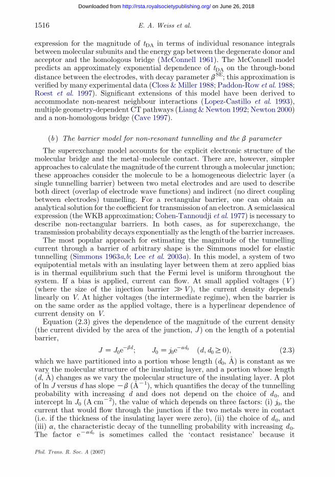
expression for the magnitude of tDA in terms of individual resonance integralsbetween molecular subunits and the energy gap between the degenerate donor andacceptor and the homologous bridge (McConnell 1961). The McConnell modelpredicts an approximately exponential dependence of tDA on the through-bonddistance between the electrodes, with decay parameter bSE; this approximation isverified by many experimental data (Closs &Miller 1988; Paddon-Row et al. 1988;Roest et al. 1997). Significant extensions of this model have been derived toaccommodate non-nearest neighbour interactions (Lopez-Castillo et al. 1993),multiple geometry-dependent CT pathways (Liang &Newton 1992; Newton 2000)and a non-homologous bridge (Cave 1997).
(b ) The barrier model for non-resonant tunnelling and the b parameter
The superexchange model accounts for the explicit electronic structure of themolecular bridge and the metal–molecule contact. There are, however, simplerapproaches to calculate the magnitude of the current through a molecular junction;these approaches consider the molecule to be a homogeneous dielectric layer (asingle tunnelling barrier) between two metal electrodes and are used to describeboth direct (overlap of electrode wave functions) and indirect (no direct couplingbetween electrodes) tunnelling. For a rectangular barrier, one can obtain ananalytical solution for the coefficient for transmission of an electron. A semiclassicalexpression (the WKB approximation; Cohen-Tannoudji et al. 1977) is necessary todescribe non-rectangular barriers. In both cases, as for superexchange, thetransmission probability decays exponentially as the length of the barrier increases.
The most popular approach for estimating the magnitude of the tunnellingcurrent through a barrier of arbitrary shape is the Simmons model for elastictunnelling (Simmons 1963a,b; Lee et al. 2003a). In this model, a system of twoequipotential metals with an insulating layer between them at zero applied biasis in thermal equilibrium such that the Fermi level is uniform throughout thesystem. If a bias is applied, current can flow. At small applied voltages (V )(where the size of the injection barrier [V ), the current density dependslinearly on V. At higher voltages (the intermediate regime), when the barrier ison the same order as the applied voltage, there is a hyperlinear dependence ofcurrent density on V.
Equation (2.3) gives the dependence of the magnitude of the current density(the current divided by the area of the junction, J ) on the length of a potentialbarrier,
J Z J0eKbd; J0 Z j0e
Kad0 ðd; d0R0Þ; ð2:3Þwhich we have partitioned into a portion whose length (d0, A) is constant as wevary the molecular structure of the insulating layer, and a portion whose length(d, A) changes as we vary the molecular structure of the insulating layer. A plotof ln J versus d has slope Kb (AK1), which quantifies the decay of the tunnellingprobability with increasing d and does not depend on the choice of d0, andintercept ln J0 (A cmK2), the value of which depends on three factors: (i) j0, thecurrent that would flow through the junction if the two metals were in contact(i.e. if the thickness of the insulating layer were zero), (ii) the choice of d0, and(iii) a, the characteristic decay of the tunnelling probability with increasing d0.The factor eKad0 is sometimes called the ‘contact resistance’ because it
Phil. Trans. R. Soc. A (2007)
1517Charge transport through organic films
on June 26, 2018http://rsta.royalsocietypublishing.org/Downloaded from
quantifies the characteristics (height and length) of the tunnelling barrier thatthe electron encounters at interface between the metal and the molecule(Engelkes et al. 2004).
An electron may tunnel through the junction via multiple pathways, somethat follow the carbon backbone of the molecule and some that involve multiplemolecules. For close-packed SAMs of n-alkanethiolate, for example, themagnitude of the tunnelling current appears to correlate with the molecularlength, i.e. the distance between the electrodes along the molecular axis, and notwith the average shortest physical distance between the electrodes.
The parameter b has been used as a benchmark for the suitability of amolecule as a wire: the smaller the value of b, the longer the distance over whichcharge can be transferred without penalty. The b parameter is often used tocharacterize all types of transport, although from its very definition it onlyapplies to exponentially decaying processes. The range of b values found foridentical bridge units measured in solution and through SAMs of organic thiolson the surface of metal electrodes (e.g. bZ0.6–1.2 AK1 for alkanes (Leland et al.1985; Oevering et al. 1987; Closs & Miller 1988; Chidsey 1991; Finklea &Hanshewm 1992; Paulson et al. 1993; Paddon-Row 1994; Slowinski et al. 1997;Klan 1998; Holmlin et al. 2001; Cui 2002a,b; Selzer et al. 2002; Xu & Tao2003; Weiss et al. 1998), bZ0.32–0.66 AK1 for oligophenylene (Kim & Lieber1989; Osuka et al. 1990, 1993; Helms et al. 1991, 1992; Barigelletti et al. 1994,1996; Holmlin et al. 2001; Weiss et al. 2004), bZ0.06–0.5 AK1 for oligo-(phenyleneethynylene)s (OPEs) and oligo(phenylenevinylene) (OPVs) (Sachs
et al. 1997; Creager 1999; Sikes et al. 2001), bZ0.04–0.2 AK1 for oligoenes(Benniston et al. 1994; Osuka et al. 1996) and bZ0.04–0.17 AK1 for oligoynes(Marczinke 1994; Grosshenny et al. 1995; Osuka et al. 1995)) reflects the factthat the most fundamental aspects of transport, including length dependence, aresensitive to the environment in which the measurement is performed.
The Simmons model (and variations) have been used successfully to fitexperimentally measured current densities in a variety of systems (Cui 2002b;Chen2003;York&Slowinsky 2003; Lee et al. 2004), but thismodel ignores thedetailsof the electronic structure of the molecule and the geometry of the contacts andneglects electron–electron interactions that are captured by more sophisticatedelectronic structure theory (Nitzan 2001; Reimers et al. 2002; Xue et al. 2002). Themodel, therefore, gives no real insight into either the mechanism of CT throughthe junction or modifications that might be made on the molecular level to optimizethe performance of the junction. Furthermore, while the single-barrier model mayadequately describe electron conduction in some cases, it does not lend itself to thedescription of hole conduction (an inherentlymulti-step process), which is thought tobe the dominant mechanism of CT through many saturated and conjugatedmolecular bridges. In contrast, the inputs for calculations of superexchange couplingcan, in principle, incorporate everything known about the electronic structure of thejunction because these inputs are taken from the Hamiltonian of the system.
(c ) Thermally activated hopping transport
If the Fermi level of the injecting electrode and the energy of the relevantbridge orbital(s) are within several kBT of resonance, such that thermal injectionis relatively facile (as is often found for p-systems and high temperatures), the
Phil. Trans. R. Soc. A (2007)

E. A. Weiss et al.1518
on June 26, 2018http://rsta.royalsocietypublishing.org/Downloaded from
conduction of electrons or holes will occur through the molecular orbitals, eithervia resonant tunnelling (for weak vibronic coupling, as in carbon nanotube wires)or localized hopping, if the vibronic coupling is stronger (Cave & Newton 1997;Berlin et al. 2002; Weiss et al. 2004; Berlin & Ratner 2005). For long distances,the incoherent, ‘wire-like’ channel is generally more efficient than the coherentone (because, for processes whose rate decays exponentially with distance, thetotal rate of a series of very short-distance processes is greater than the rate ofone very long-distance process; Davis et al. 1997, 1998; Jortner et al. 1998).Incoherent hopping is the dominant mechanism of efficient hole and electrontransport over long (approx. 1–1000 nm) distances within films of undoped,conjugated polymers and molecular crystals.
The transition from tunnelling-type transport (weakly temperature dependentand strongly length dependent) to incoherent hopping (strongly temperaturedependent and weakly length dependent) has also been observed in singlemolecule break junctions (Anariba & McCreery 2002; Selzer et al. 2004a,b, 2005;Haiss et al. 2006). In the case of single molecules, the mechanism switch mostoften results from the thermal activation of vibrational or torsional modes; thisactivation improves conjugation within the molecule and stabilizes its oxidized orreduced state. Charge is then injected into the newly thermally accessiblemolecular orbital, where it may hop along the molecular bridge until it isabsorbed by the counter electrode.
3. Tools for the study of charge transport through organicmolecules: SAMs and the mercury-drop junction
The measurement of a current–voltage response on a single molecule within ajunction is, in principle, the ideal method of characterizing the electrical propertiesof single molecules. Indeed, the conductances of single molecule transportjunctions—usually within mechanically controllable or electrochemical breakjunctions (Reed et al. 1997; Reinerth et al. 1998; Xu & Tao 2003; Selzer et al.2004a,b, 2005;Gupta et al. 2004;Xiao et al. 2004)—havedisplayed the characteristicfluctuations that are analogous to the ‘blinkings’ observed in single-moleculespectroscopy, probably due to different geometries of the molecule or surroundingmolecules (Donhauser 2001; Xiao et al. 2004). The collection of many data usingsophisticated single-molecule measurements is, however, challenging experimen-tally. An alternative strategy is to arrange macroscopic quantities of molecules inordered SAMs (Barigelletti et al. 1994; Benniston et al. 1994; Osuka et al. 1995;Cave&Newton 1997; Sachs et al. 1997; Jortner et al. 1998; Sikes et al. 2001; Reimerset al. 2002; Chen 2003), and then electrically address these molecules en masse, insmall groups, or individually. SAMs of saturated hydrocarbons (Troughton et al.1988; Bain & Whitesides 1989; Bain et al. 1989; Nuzzo et al. 1990; Labinis et al.1991a; Dubois & Nuzzo 1992; Allara 1995; Ulman 1996; Reed et al. 1997; Zhouet al. 1997; Reinerth et al. 1998; Bumm et al. 1999; Wold & Frisbie 2000; Cui 2001;Holmlin et al. 2001; Beebe et al. 2002; Rampi & Whitesides 2002; Wold et al. 2002;Love et al. 2003;Naaman&Vager 2003;Wang et al. 2003a; Engelkes et al. 2004;Tranet al. 2004, 2005; Lewis et al. 2005; Selzer et al. 2005; Weiss et al. 1998) and con-jugated oligomers (oligophenylenes (Liao et al. 2000; Heister et al. 2001; Anariba &McCreery 2002; Lee et al. 2003b; McCreery 2004; Shaporenko et al. 2005),
Phil. Trans. R. Soc. A (2007)

1519Charge transport through organic films
on June 26, 2018http://rsta.royalsocietypublishing.org/Downloaded from
oligophenylenevinylenes (Joachim 1999; Dudek et al. 2001; Sikes et al. 2001;Reichert et al. 2002), oligophenylenethylenes and carotenes (Leatherman 1999;Ramachandran 2003)) have been the basic building block for the majority of MIMjunctions. The chemistry of the formation of SAMs on many metal, semiconductor(Selzer & Cahen 2001; Selzer et al. 2002; Vilan & Cahen 2002b; Salomon et al. 2003;Haick et al. 2004) and carbon (Ranganathan et al. 2001; Anariba &McCreery 2002)substrates is well understood, and the structure of SAMs—both within the film andat the substrate–organic interface—has been characterized via X-ray diffraction,X-ray photoemission spectroscopy and infrared spectroscopy.
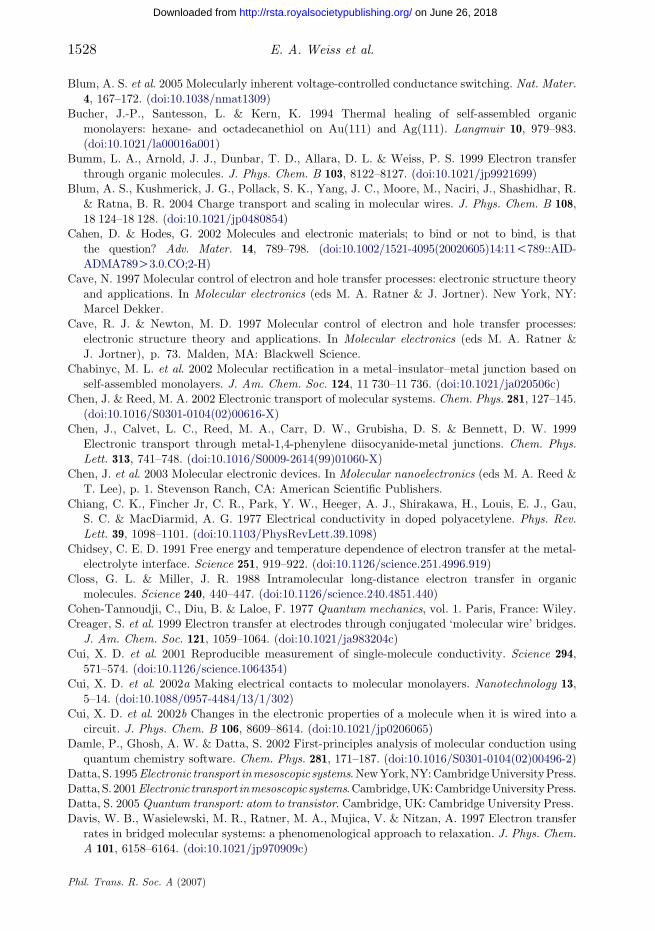
The very first MIM junction (MIM) used to study the electrical properties ofmonolayer films was assembled by condensing evaporated metal (Pb, Ag and Al)on top of a Langmuir–Blodgett (LB) film deposited on an Al surface (Honig1976). Several researchers still use the same technique to study the electricalbehaviour of molecules incorporated in a LB film. In recent years, a large varietyof conceptually new junctions have been designed to measure the currentdensities through a single molecule or few molecules within a SAM, includingSTM (Han 1997; Bumm et al. 1999; Zeng et al. 2002; Monnell et al. 2005; Haisset al. 2006; Weiss et al. 1998), conducting AFM (cAFM; Kelley et al. 1999;Leatherman 1999; Wold & Frisbie 2000; Beebe et al. 2002; Cui 2002a; Rawlettet al. 2002; Wold et al. 2002; Ramachandran 2003; Engelkes et al. 2004; Engelkeset al. 2005), gold nanoparticle-mediated cAFM (Cui 2001, 2002b), nanopore(Zhou et al. 1997; Chen et al. 1999; Lee et al. 2003a; Wang et al. 2003a,b),crosswire (Blum 2005) and in-wire junctions (Kratochvilova et al. 2002a; Blumet al. 2004). Each type of junction has specific advantages and disadvantageswith respect to fabrication, reproducibility and application. In many cases, theinterpretation of the results of STM experiments is difficult due to theconvolution of the tip–substrate distance with the conductance. ConductingAFM obviates this problem by controlling the position of the metal-coated tipwith respect to the substrate using force feedback. Nanofabrication results injunctions able to trap a much smaller number of molecules: the evaporation ofgold through a nanopore mask on top of a SAM reduces the area of the junctionto less than 300 mm2, and therefore reduces the probability of incorporatingdefects in the junctions (but also the current). Although these systems havedemonstrated interesting functionalities, there has been little characterization(Zhu et al. 2006; Walker et al. 2007) of the nature of the interface formed by theevaporation of metal atoms onto organic films, and electrical shorts due to thepercolation of Au atoms through the film (and probably other types of defects)have limited the reproducibility of the results.
Junctions designed to incorporate a large number of molecules usually consistof a metal surface electrode supporting a SAM of organic molecules, and a secondelectrode that is formed by deposition of evaporated gold onto the organic layer(Wang et al. 2004b). The evaporation of the second electrode without damagingthe fragile molecular layer and inducing electrical shorts between the twoelectrodes still presents a challenge. In an attempt to circumvent this problem, anumber of different strategies such as lift-off float-on Au pads (Xu et al. 2002) ordeposition of cold gold (Xu et al. 2002) have been employed successfully.Although these approaches have produced laboratory test structures, they aredifficult to scale up for the fabrication of circuits or molecular devices becausethey are highly specialized and time consuming. Recently, nano-transfer printing
Phil. Trans. R. Soc. A (2007)
Hg
Hg
(a) Hg surface
S
X
S
X
S
X
S
X
S
X
S
X
S
X
Au surface
S S S S SSS SS SS SS SS SSSSSS
Y Y Y Y YYY
(b)
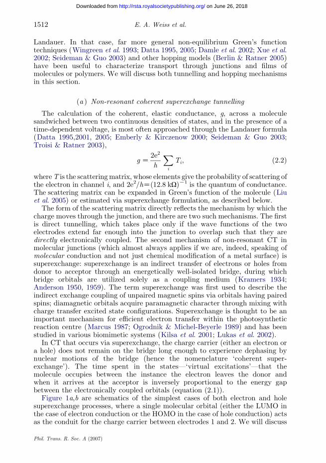
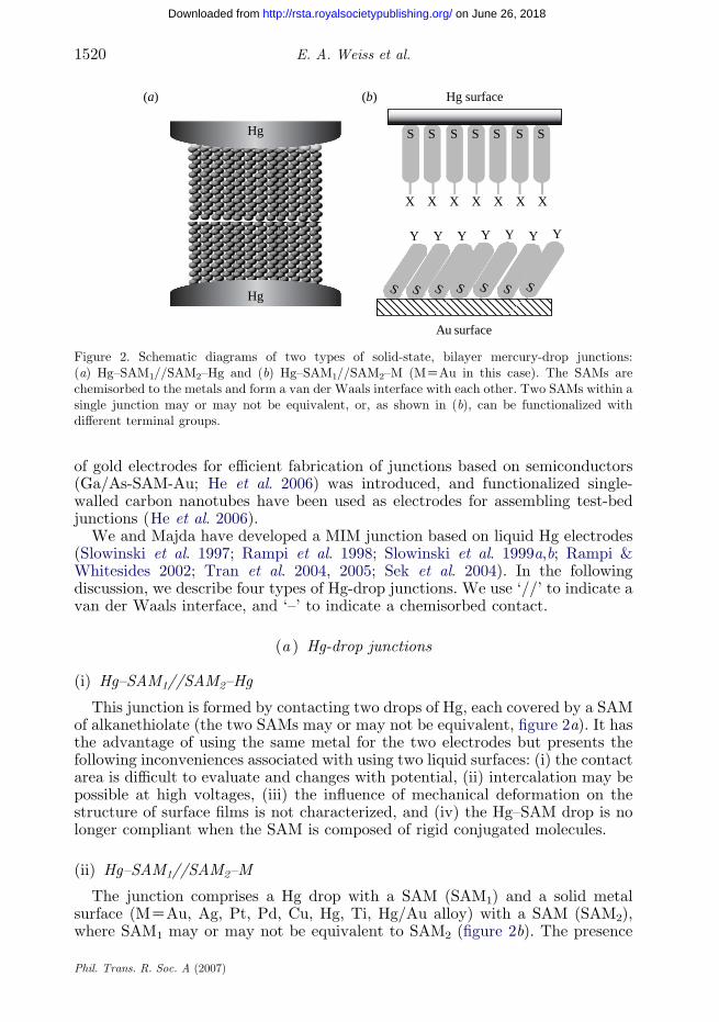
Figure 2. Schematic diagrams of two types of solid-state, bilayer mercury-drop junctions:(a) Hg–SAM1//SAM2–Hg and (b) Hg–SAM1//SAM2–M (MZAu in this case). The SAMs arechemisorbed to the metals and form a van der Waals interface with each other. Two SAMs within asingle junction may or may not be equivalent, or, as shown in (b), can be functionalized withdifferent terminal groups.
E. A. Weiss et al.1520
on June 26, 2018http://rsta.royalsocietypublishing.org/Downloaded from
of gold electrodes for efficient fabrication of junctions based on semiconductors(Ga/As-SAM-Au; He et al. 2006) was introduced, and functionalized single-walled carbon nanotubes have been used as electrodes for assembling test-bedjunctions (He et al. 2006).
We and Majda have developed a MIM junction based on liquid Hg electrodes(Slowinski et al. 1997; Rampi et al. 1998; Slowinski et al. 1999a,b; Rampi &Whitesides 2002; Tran et al. 2004, 2005; Sek et al. 2004). In the followingdiscussion, we describe four types of Hg-drop junctions. We use ‘//’ to indicate avan der Waals interface, and ‘–’ to indicate a chemisorbed contact.
(a ) Hg-drop junctions
(i) Hg–SAM1//SAM2–Hg
This junction is formed by contacting two drops of Hg, each covered by a SAMof alkanethiolate (the two SAMs may or may not be equivalent, figure 2a). It hasthe advantage of using the same metal for the two electrodes but presents thefollowing inconveniences associated with using two liquid surfaces: (i) the contactarea is difficult to evaluate and changes with potential, (ii) intercalation may bepossible at high voltages, (iii) the influence of mechanical deformation on thestructure of surface films is not characterized, and (iv) the Hg–SAM drop is nolonger compliant when the SAM is composed of rigid conjugated molecules.
(ii) Hg–SAM1//SAM2–M
The junction comprises a Hg drop with a SAM (SAM1) and a solid metalsurface (MZAu, Ag, Pt, Pd, Cu, Hg, Ti, Hg/Au alloy) with a SAM (SAM2),where SAM1 may or may not be equivalent to SAM2 (figure 2b). The presence
Phil. Trans. R. Soc. A (2007)
1521Charge transport through organic films
on June 26, 2018http://rsta.royalsocietypublishing.org/Downloaded from
of a solid surface increases the versatility of the junction dramatically because:(i) one can characterize the organization of the molecules forming the SAM on asolid surface using infrared spectroscopy or other methods, (ii) the supramole-cular structure of a SAM can be adjusted by changing the metal substrate: bothsaturated and conjugated chains have different tilt angle on Ag than on Ausurfaces, and (iii) the contact area can be evaluated easily.
(iii) Electrochemical junctions: Hg–SAM1–R//R–SAM2–Hg and Hg–SAM1//R//SAM2–Hg
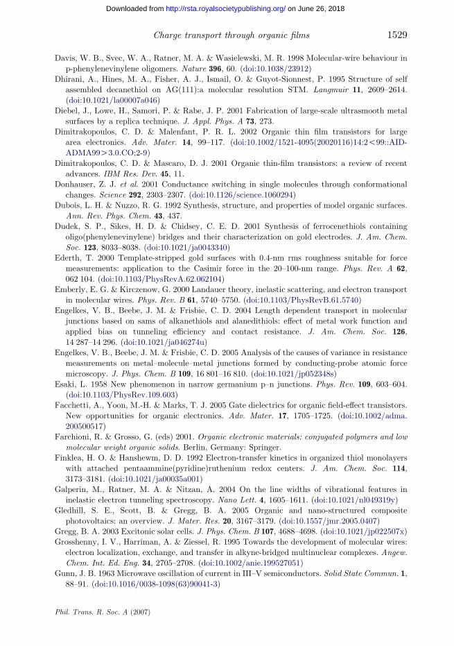
Two-electrode systems suffer from an ambiguity in the relative positions of theFermi levels of the electrodes and the energy levels of the redox moleculessandwiched between them. In an electrochemical cell, however, a referenceelectrode relates the potential of a working electrode to energy levels of moleculesin solution. We have assembled an electrochemical junction, figure 3a, thatallows us to fix the potential of the electrodes with respect to the oxidationpotential, E o, of the incorporated redox centre, R (equal to a ruthenium-terminated thiol, HS(CH2)10CONHCH2pyRu(NH3)5). We placed the Hgelectrodes, together with an Ag/AgCl reference electrode and a platinumcounter electrode, in an electrolyte solution, and controlled the potentials of theelectrodes by connecting them to a bipotentiostat.
We have designed, assembled and studied two different electrochemicaljunctions that incorporate redox sites. Figure 3 shows schematically theinterfaces of the two junctions: one where the Hg electrodes are functionalizedby thiolate monolayers that are covalently bound to redox sites (Hg–SAM1–R//R–SAM2–Hg, figure 3b), and one where the redox sites are incorporated into theinter-electrode gap (Hg–SAM1//R//SAM2–Hg, figure 3c). In both junctions, thepotentials of the mercury electrodes are driven in such a way that one electrode(the cathode) acts as the electron donor and the other one (the anode) as theelectron acceptor. We measured the current between the electrodes by keepingthe potential of one electrode constant and sweeping the potential of the other
electrode across the oxidation potential of the RuII/III redox couple.The redox sites, R, are incorporated between the electrodes within the
Hg–SAM//R//SAM–Hg junction (figure 3c) by trapping them via electrostaticinteractions at the interface of the SAMs of alkanethiolate terminated withcarboxylic acid groups. We selected the carboxylic acid functionality as the headgroup for two reasons: (i) carboxylic acid tail groups can be ionized at pHO4, soCOOK moieties attract the positively charged Ru(NH3)6
3C ions at the surface ofthe SAM and (ii) the defects caused by electrostatic repulsion between theCOOK terminating groups allow the Ru(NH3)6
3C ions to access the surfaces ofthe electrodes. To assemble the junction, we extruded two Hg drops from twomicrosyringes, both of which are immersed in a solution of 11-mercaptodecanoicacid (HSC10COOH) to form the carboxylic-terminating SAMs. After rinsing,they are placed in a solution of Ru(NH3)6
3C. When they are brought in contactby a micromanipulator, the redox sites are trapped between the two electrodes.
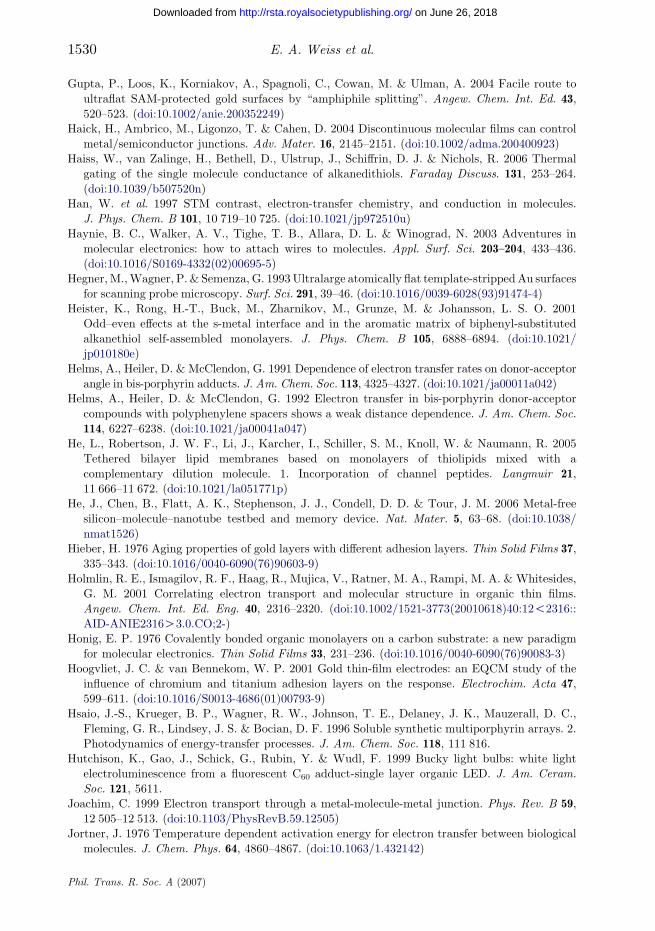
Figure 4 shows a plot of log J for Hg-drop junctions incorporating SAMs ofn-alkanethiolates versus the total number of carbons in the alkyl chain(s)between the electrodes in the junction (Weiss et al. 2007). A linear least-squaresfit (R2Z0.971) to the largest dataset—that collected at VZ0.4–0.5 V—yields
Phil. Trans. R. Soc. A (2007)

to potentiostatreferenceelectrodecounterelectrode
solution ofelectrolyteand analyte
Hg
R R R R
Hg
syringewith Hg
(a)
HS(CH2)12(Ru(NH3)5py)2+
(b)
Ru(NH3)63+
(c)
Figure 3. (a) Diagram of the electrochemical mercury-drop junction. The inset is a close-up ofredox centres that are trapped at the interface of the two SAMs (each chemisorbed to mercury) toform the junction Hg–SAM1//R//SAM2–Hg. A less-idealized cartoon of this type of interface isshown in (c). (b) A cartoon of the interface formed when two SAMs on mercury, each covalentlybonded to a redox centre, are contacted to form the junction Hg–SAM1–R//R–SAM2–Hg.
E. A. Weiss et al.1522
on June 26, 2018http://rsta.royalsocietypublishing.org/Downloaded from
bZ1.1/carbon (0.85 AK1). Aggregated dataset 2 (the solid circles) containsvalues of J measured at VZK1.5 V (in an electrochemical setup). For thisdataset, bZ0.86/methylene group (0.69 AK1), and J0Z1.7!102 AcmK2.
4. Reproducibility of measurements of charge transport
Efforts to interpret and use several types of remarkable phenomena that havebeen observed in organic and molecular-scale devices—phenomena such asmolecular rectification (Ranganathan et al. 2001; Chabinyc 2002; Vilan et al.2003) and negative differential resistance (Esaki 1958; Gunn 1963; Sollner et al.1983; Rawlett et al. 2002; Chen & Reed 2002; Kratochvilova et al. 2002b)—have
Phil. Trans. R. Soc. A (2007)

aggregated dataset 2:V = –1.5 V, b = 0.86/NCJ0 = 1.7×10² A cm–2
aggregated dataset 1:V = 0.4 –0.5 V, b = 1.1/NCJ0 =1.0×10⁶ A cm–2
TS surfaces:V = 0.5 V, b = 0.71/NCJ0 = 7.9×10² A cm–2
0 5 10 15 20 25 30 35 4010–11
10–9
10–7
10–5
10–3
10–1
101
103
105
|J| (
Acm
–2)
NC
Figure 4. Log J for Hg-drop junctions incorporating SAMs of n-alkanethiolates versus the totalnumber of carbons in the alkyl chain(s) between the electrodes in the junction. The slope of thelinear least-squares fit to these data is b/2.3. In the calculation of b, all points are weighted equally.Aggregated dataset 1 (the solid diamonds and open squares) includes values of J measured atVZ0.4 or 0.5 V (the solid diamonds are data acquired using template-stripped surfaces, see text).For this dataset, bZ1.1/methylene group (0.85 AK1), and J0Z1.0!106 A cmK2. Aggregateddataset 2 (the solid circles) contains values of J measured at VZK1.5 V. For this dataset,bZ0.86/methylene group (0.69 AK1), and J0Z1.7!102 A cmK2. (Reprinted with permission fromthe Journal of the American Chemical Society)
1523Charge transport through organic films
on June 26, 2018http://rsta.royalsocietypublishing.org/Downloaded from
been hampered by the inability of researchers to duplicate each other’s results oreven construct identical devices and junctions on which to obtain these results.Differing degrees of both intramolecular disorder within the organic film anddefects at the metal–organic interfaces (caused by defects in or impurities on theelectrodes or the use of different methods of film deposition) are two majorsources of irreproducibility of electrical measurements. For devices where currentis limited by transport through the bulk, i.e. organic devices where the film ishundreds of nanometers thick, variation in intermolecular order (usually due tovariation in the morphology of the polymer film) is a major cause of discrepanciesin performance from device to device. For molecular-scale electronic devices,where the organic film is, at most, tens of angstroms thick, CT across the metal–molecule interfaces is often the rate-limiting step; furthermore, the currentsthrough these devices may be masked by defect-mediated current (caused byfilaments between the electrodes or contact of the electrodes with disorderedsections of the SAM).
(a ) Survey of defects in SAMs formed on metal substrates
Many of the defects that occur at the metal–organic interface of a SAM on ametal substrate have the potential to contribute to (or even dominate) thecurrent through the SAM. For instance, migration of metal atoms from thesurface of one electrode to the second electrode may result in a highly conductive
Phil. Trans. R. Soc. A (2007)

E. A. Weiss et al.1524
on June 26, 2018http://rsta.royalsocietypublishing.org/Downloaded from
pathway (or filament) between the electrodes through which electrons can travel(Haynie et al. 2003). In the case of SAMs of n-alkanethiolates, step edges andgrain boundaries in the metal surface probably result in ‘thin areas’ of the SAM,where the molecules are not trans-extended and the top electrode contacts adisordered region of the SAM; this type of defect may result in a reduced lengthof the through-bond pathway between the electrodes and increased current(compared with that through the all-trans molecules). Vacancy islands formwhen individual metal (usually silver) atoms dissociate from the plane of themetal surface upon formation of the thiolate bond and migrate to form raisedislands (Laibinis et al. 1991b; Bucher et al. 1994; Dhirani et al. 1995). Thereorganization process leaves behind vacancies of one or a few metal atoms thatare one atomic step (approx. 0.5 nm for silver) below the surface; isolatedvacancies may also anneal into larger vacancy islands (Bucher et al. 1994;Dhirani et al. 1995; Yamada et al. 2000). Raised vacancy islands form whenmetal atoms do not migrate to step edges, but rather form small clusters on thesurface that are one atomic step above the surrounding atoms. The molecules onraised vacancy islands are not stabilized by the molecular lattice and maybecome disordered (or perhaps deformed) under the pressure of the top electrode(Love et al. 2005). If solvent is present in the junction (such as in the case ofmany mercury-drop junctions; Chabinyc 2002; Tran et al. 2005), solventmolecules may become trapped within a gap at metal//SAM or SAM//SAM(in the case of bilayer junctions) van der Waals interfaces when a molecule‘kinks’, i.e. bends over within the SAM and curls away from the top contact. Ifone chain bends, another chain will bend on top of it, and packing of the terminalends of the chains of the few surrounding molecules will be disordered relative tothat of trans-extended chains. Molecules may kink due to, for example, thepresence of grain boundaries or step edges in the metal film or impurities insolvents and reagents that deposit on the metal surface during SAM formationand cause irregularities in the metal lattice (Hieber 1976; Laibinis et al. 1991b;Hoogvliet & van Bennekom 2001).
(b ) Formation of ultrasmooth substrates using template-stripping
One way to minimize the frequency of defects at the electrode–organicinterface and within the bulk of the organic layer is to start with an atomicallysmooth electrode. Ultrasmooth metal substrates—those with low root-mean-squared (RMS) roughness and large, flat grains (compared with that of the filmscharacterized as deposited, AS-DEP, by e-beam evaporation)—produced withthe general method of template stripping (TS; Wagner et al. 1995) have provento be useful in the study and application of well-ordered SAMs (Wagner et al.1995; Hsaio et al. 1996; Diebel et al. 2001; Unal et al. 2002; Naumann et al. 2003;Ragan et al. 2004; Zhou et al. 2004; Engelkes et al. 2005; He et al. 2005).Recently, we developed a procedure (Weiss et al. in preparation) by which weprepared ultrasmooth metal films by evaporating the metal onto a silicon wafersupporting a native oxide layer (the ultraflat ‘template’; Hegner et al. 1993;Samori et al. 1999; Ederth 2000; Diebel et al. 2001; Unal et al. 2002; Naumann2003; Rossetti et al. 2003; Gupta et al. 2004; Ragan et al. 2004; Engelkes et al.2005), attaching a mechanical support—either a composite of a glass slide andoptical adhesive (glass/OA), a composite of polydimethylsiloxane and optical
Phil. Trans. R. Soc. A (2007)
(a)
– 0.4 – 0.2 0 0.2 0.410–12
10–10
10–8
10–6
10–4
10–2
100cu
rren
t den
sity
(A
cm–2
)
applied voltage (V)
(b)
– 0.4 0.2 0.4applied voltage (V)– 0.2 0
Ag–SC14//C14S–Hg
Figure 5. (a) Plot of the average jJ jKV curves (bold black line) and all jJ jKV curves (light greylines) measured on the TS junctions Ag–SC14//C14S–Hg, except for the initial traces that had acurrent density several orders of magnitude below the remaining traces, and traces directlypreceding and following amalgamation. (b) The same set of traces for the corresponding junctionusing AS-DEP silver. (No averages were calculated for these data.) (Reprinted with permissionfrom the Journal of the American Chemical Society)
1525Charge transport through organic films
on June 26, 2018http://rsta.royalsocietypublishing.org/Downloaded from
adhesive (PDMS/OA), or a drop of solder—to the top of the evaporated metalfilm, and cleaving the metal film from the template to expose the face of the filmthat had been adjacent to the Si/SiO2 surface. The template-stripping methodproduces, as a precursor to the ultrasmooth film, a ‘sandwich structure’ that iscomposed of the template, the film and the mechanical support. In this sandwichstructure, the template protects the functional surface of the metal film from anyenvironmental contaminants and from oxidation (even for readily oxidizedmaterials like silver); thus, we are able to store the films for at least two monthsbetween the evaporation of the film and use (or structural characterization) ofthe film, without contamination (Diebel et al. 2001; Ragan et al. 2004). We canalso separate the TS film from the protecting template by immersing thesandwich structure in a solution of thiols (chemical template stripping), suchthat the film never comes into contact with O2.
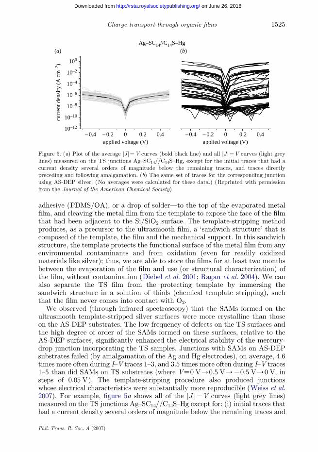
We observed (through infrared spectroscopy) that the SAMs formed on theultrasmooth template-stripped silver surfaces were more crystalline than thoseon the AS-DEP substrates. The low frequency of defects on the TS surfaces andthe high degree of order of the SAMs formed on these surfaces, relative to theAS-DEP surfaces, significantly enhanced the electrical stability of the mercury-drop junction incorporating the TS samples. Junctions with SAMs on AS-DEPsubstrates failed (by amalgamation of the Ag and Hg electrodes), on average, 4.6times more often during I–V traces 1–3, and 3.5 times more often during I–V traces1–5 than did SAMs on TS substrates (where VZ0 V/0.5 V/K0.5 V/0 V, insteps of 0.05 V). The template-stripping procedure also produced junctionswhose electrical characteristics were substantially more reproducible (Weiss et al.2007). For example, figure 5a shows all of the jJ jKV curves (light grey lines)measured on the TS junctions Ag–SC14//C14S–Hg except for: (i) initial traces thathad a current density several orders of magnitude below the remaining traces and
Phil. Trans. R. Soc. A (2007)

E. A. Weiss et al.1526
on June 26, 2018http://rsta.royalsocietypublishing.org/Downloaded from
(ii) traces directly preceding and following amalgamation. Figure 5b contains thesame set of traces for the corresponding AS-DEP junctions. Use of ultraflat Ag as
the substrate for the SAM decreased the range in measured values of J by 106.
5. Future directions and additional remarks
There are three especially promising directions for the mercury-drop junction asfollows. (i) The junction has proven useful for the measurement of current–voltage characteristics (both dark and under illumination) of ordered films ofsemiconductor nanocrystals. Glass coated with indium tin oxide (ITO) is acommon substrate for these films because it allows the films to be incorporatedinto solar cells and photodetectors; ITO is also a convenient ‘bottom contact’within the mercury-drop junction because it does not amalgamate with mercury.Preliminary experiments indicate that I–V curves for these films with mercury asa top contact are reproducible. (ii) We are designing and constructing a systemby which pressurized flow of mercury through microchannels positions hundredsto thousands of mercury drops above SAMs that have been patterned on acommon substrate; these drops are then extruded simultaneously andindividually electrically addressed in order to parallelize the I–V measurement.In this way, we can gather meaningful statistics on current densities andefficiently screen organic molecules for their potential as components inelectronic devices. (iii) Much of the irreproducibility in the measurements ofcurrent density using the mercury-drop junction comes from the fact that themercury drop consistently amalgamates with the bottom electrode if themeasurement is not performed under solvent (usually hexadecane) or a solutionof thiol. Solvent molecules then become trapped at the SAM//SAM interface andcause heterogeneity in the topography of this interface. The replacement ofmercury, which is also problematic owing to its high reactivity withenvironmental contaminants, with a eutectic metal—specifically, an indium/gallium alloy that is a liquid at room temperature—alleviates many of theseproblems. In/Ga does not amalgamate with the metals commonly used assubstrates for SAMs, it does not (to our knowledge) react readily with thiolcontaminants, and it may be ‘pulled’ to create a junction with a diameterapproximately 10 times smaller than that which may be formed with themercury drop. We can, therefore, perform these measurements ‘dry’, i.e. in theabsence of a solvent bath, and smaller junctions, in general, incorporate fewerdefects and lead to a smaller range in values of current density measured for agiven junction than do larger junctions. Currently, we are pursuing all three ofthese directions.
A final, more general, note is that in the fields of both organic and molecular-scale electronics, there still exists a major difference in philosophy betweenchemists and engineers. Chemists often concentrate on molecular properties ofthe organic bulk within a device or junction without considering the effect ofinterfacing the organic material with the metal electrodes. Engineers understandthe properties of interfaces (tunnelling barriers, diodes, etc.) but often do not payattention to the fact that organic molecules cannot always be treated as bulkdielectric layers. A molecule is a spatially and energetically diverse (andenvironment-sensitive) landscape, and the electronic structure of a molecule is,
Phil. Trans. R. Soc. A (2007)
1527Charge transport through organic films
on June 26, 2018http://rsta.royalsocietypublishing.org/Downloaded from
by definition, responsible for its electronic properties, both within the bulk and atan interface with another material. Both characteristics—the molecular andsupramolecular structure of the organic material and the nature of the metal–organic interface—are equally important in determining the performance of thedevice. Theorists have recognized this fact and have designed programmes toincorporate explicit electronic structure in the bulk and at the interface, but donot yet have the tools to predict the characteristics of junctions with more than afew molecules and a few metal atoms.
We acknowledge funding from NSF CHE-0518055, DARPA, and use of the shared facilitiessupported by NSEC under award PHY-0117795, and by MRSEC under award DMR-0213805.E.A.W. thanks the Petroleum Research Fund of the American Chemical Society for a fellowship(PRF no. 43083-AEF).
References
Allara, D. L. 1995 Critical issues in applications of self-assembled monolayers. Biosens. Bioelec. 10,771–783. (doi:10.1016/0956-5663(95)99215-7)
Anariba, F. & McCreery, R. L. 2002 Electronic conductance behavior of carbon-based molecularjunctions with conjugated structures. J. Phys. Chem. B 106, 10 355–10 362. (doi:10.1021/jp026285e)
Anderson, P. W. 1950 Antiferromagnetism. Theory of superexchange interaction. Phys. Rev. 79,350–356. (doi:10.1103/PhysRev.79.350)
Anderson, P. W. 1959 New approach to the theory of superexchange interactions. Phys. Rev. 115,2–13. (doi:10.1103/PhysRev.115.2)
Aviram, A. & Ratner, M. A. 1974 Molecular rectifiers. Chem. Phys. Lett. 29, 277–283. (doi:10.1016/0009-2614(74)85031-1)
Bain, C. D. & Whitesides, G. M. 1989 Formation of monolayers by the coadsorption of thiols ongold: variation in the length of the alkyl chain. J. Am. Chem. Soc. 111, 7164–7175. (doi:10.1021/ja00200a040)
Bain, C. D., Troughton, E. B., Tao, Y.-T., Evall, J., Whitesides, G. M. & Nuzzo, R. G. 1989Formation of monolayer films by the spontaneous assembly of organic thiols from solution ontogold. J. Am. Chem. Soc. 111, 321–335. (doi:10.1021/ja00183a049)
Barigelletti, F., Flamigni, L., Balzani, V., Collin, J.-P., Sauvage, J.-P., Sour, A., Constable, E. C.& Cargill Thompson, A. M. W. 1994 Rigid rod-like dinuclear Ru(II)/Os(II) terpyridine-typecomplexes. electrochemical behavior, absorption spectra, luminescence properties, andelectronic energy transfer through phenylene bridges. J. Am. Chem. Soc. 116, 7692–7699.(doi:10.1021/ja00096a028)
Barigelletti, F., Flamigni, L., Guardgli, M., Juris, A., Beley, M., Chodorowsky-Kimmes, S., Collin,J.-P. & Sauvage, J.-P. 1996 Energy transfer in rigid Ru(II)/Os(II) dinuclear complexes withbiscyclometalating bridging ligands containing a variable number of phenylene units. Inorg.Chem. 35, 136–142. (doi:10.1021/ic9503085)
Beebe, J. M., Engelkes, V. B., Miller, L. L. & Frisbie, C. D. 2002 Contact resistance inmetal–molecule–metal junctions based on aliphatic SAMs: effects of surface linker and metalwork function. J. Am. Chem. Soc. 124, 11 268–11 269. (doi:10.1021/ja0268332)
Benniston, A. C., Goulle, V., Harriman, A., Lehn, J.-M. & Marczinke, B. 1994 Electrondelocalization in polyene–bridged binuclear complexes. J. Phys. Chem. 98, 7798–7804. (doi:10.1021/j100083a009)
Berlin, Y. A. & Ratner, M. A. 2005 Intra-molecular electron transfer and electric conductance viasequential hopping: unified theoretical description. Radiat. Phys. Chem. 74, 124.
Berlin, Y. A., Burin, A. L. & Ratner, M. A. 2002 Elementary steps for charge transport in DNA:thermal activation vs. tunneling. Chem. Phys. 275, 61–74. (doi:10.1016/S0301-0104(01)00536-5)
Phil. Trans. R. Soc. A (2007)
E. A. Weiss et al.1528
on June 26, 2018http://rsta.royalsocietypublishing.org/Downloaded from
Blum, A. S. et al. 2005 Molecularly inherent voltage-controlled conductance switching. Nat. Mater.
4, 167–172. (doi:10.1038/nmat1309)
Bucher, J.-P., Santesson, L. & Kern, K. 1994 Thermal healing of self-assembled organic
monolayers: hexane- and octadecanethiol on Au(111) and Ag(111). Langmuir 10, 979–983.
(doi:10.1021/la00016a001)
Bumm, L. A., Arnold, J. J., Dunbar, T. D., Allara, D. L. & Weiss, P. S. 1999 Electron transfer
through organic molecules. J. Phys. Chem. B 103, 8122–8127. (doi:10.1021/jp9921699)
Blum, A. S., Kushmerick, J. G., Pollack, S. K., Yang, J. C., Moore, M., Naciri, J., Shashidhar, R.
& Ratna, B. R. 2004 Charge transport and scaling in molecular wires. J. Phys. Chem. B 108,
18 124–18 128. (doi:10.1021/jp0480854)
Cahen, D. & Hodes, G. 2002 Molecules and electronic materials; to bind or not to bind, is that
the question? Adv. Mater. 14, 789–798. (doi:10.1002/1521-4095(20020605)14:11!789::AID-
ADMA789O3.0.CO;2-H)
Cave, N. 1997 Molecular control of electron and hole transfer processes: electronic structure theory
and applications. In Molecular electronics (eds M. A. Ratner & J. Jortner). New York, NY:
Marcel Dekker.
Cave, R. J. & Newton, M. D. 1997 Molecular control of electron and hole transfer processes:
electronic structure theory and applications. In Molecular electronics (eds M. A. Ratner &
J. Jortner), p. 73. Malden, MA: Blackwell Science.
Chabinyc, M. L. et al. 2002 Molecular rectification in a metal–insulator–metal junction based on
self-assembled monolayers. J. Am. Chem. Soc. 124, 11 730–11 736. (doi:10.1021/ja020506c)
Chen, J. & Reed, M. A. 2002 Electronic transport of molecular systems. Chem. Phys. 281, 127–145.
(doi:10.1016/S0301-0104(02)00616-X)
Chen, J., Calvet, L. C., Reed, M. A., Carr, D. W., Grubisha, D. S. & Bennett, D. W. 1999
Electronic transport through metal-1,4-phenylene diisocyanide-metal junctions. Chem. Phys.
Lett. 313, 741–748. (doi:10.1016/S0009-2614(99)01060-X)
Chen, J. et al. 2003 Molecular electronic devices. In Molecular nanoelectronics (eds M. A. Reed &
T. Lee), p. 1. Stevenson Ranch, CA: American Scientific Publishers.
Chiang, C. K., Fincher Jr, C. R., Park, Y. W., Heeger, A. J., Shirakawa, H., Louis, E. J., Gau,
S. C. & MacDiarmid, A. G. 1977 Electrical conductivity in doped polyacetylene. Phys. Rev.
Lett. 39, 1098–1101. (doi:10.1103/PhysRevLett.39.1098)
Chidsey, C. E. D. 1991 Free energy and temperature dependence of electron transfer at the metal-
electrolyte interface. Science 251, 919–922. (doi:10.1126/science.251.4996.919)
Closs, G. L. & Miller, J. R. 1988 Intramolecular long-distance electron transfer in organic
molecules. Science 240, 440–447. (doi:10.1126/science.240.4851.440)
Cohen-Tannoudji, C., Diu, B. & Laloe, F. 1977 Quantum mechanics, vol. 1. Paris, France: Wiley.
Creager, S. et al. 1999 Electron transfer at electrodes through conjugated ‘molecular wire’ bridges.
J. Am. Chem. Soc. 121, 1059–1064. (doi:10.1021/ja983204c)
Cui, X. D. et al. 2001 Reproducible measurement of single-molecule conductivity. Science 294,
571–574. (doi:10.1126/science.1064354)
Cui, X. D. et al. 2002a Making electrical contacts to molecular monolayers. Nanotechnology 13,
5–14. (doi:10.1088/0957-4484/13/1/302)
Cui, X. D. et al. 2002b Changes in the electronic properties of a molecule when it is wired into a
circuit. J. Phys. Chem. B 106, 8609–8614. (doi:10.1021/jp0206065)
Damle, P., Ghosh, A. W. & Datta, S. 2002 First-principles analysis of molecular conduction using
quantum chemistry software. Chem. Phys. 281, 171–187. (doi:10.1016/S0301-0104(02)00496-2)
Datta, S. 1995Electronic transport inmesoscopic systems.NewYork,NY:CambridgeUniversityPress.
Datta,S. 2001Electronic transport inmesoscopic systems.Cambridge,UK:CambridgeUniversityPress.
Datta, S. 2005 Quantum transport: atom to transistor. Cambridge, UK: Cambridge University Press.
Davis, W. B., Wasielewski, M. R., Ratner, M. A., Mujica, V. & Nitzan, A. 1997 Electron transfer
rates in bridged molecular systems: a phenomenological approach to relaxation. J. Phys. Chem.
A 101, 6158–6164. (doi:10.1021/jp970909c)
Phil. Trans. R. Soc. A (2007)
1529Charge transport through organic films
on June 26, 2018http://rsta.royalsocietypublishing.org/Downloaded from
Davis, W. B., Svec, W. A., Ratner, M. A. & Wasielewski, M. R. 1998 Molecular-wire behaviour in
p-phenylenevinylene oligomers. Nature 396, 60. (doi:10.1038/23912)
Dhirani, A., Hines, M. A., Fisher, A. J., Ismail, O. & Guyot-Sionnest, P. 1995 Structure of self
assembled decanethiol on AG(111):a molecular resolution STM. Langmuir 11, 2609–2614.
(doi:10.1021/la00007a046)
Diebel, J., Lowe, H., Samori, P. & Rabe, J. P. 2001 Fabrication of large-scale ultrasmooth metal
surfaces by a replica technique. J. Appl. Phys. A 73, 273.
Dimitrakopoulos, C. D. & Malenfant, P. R. L. 2002 Organic thin film transistors for large
area electronics. Adv. Mater. 14, 99–117. (doi:10.1002/1521-4095(20020116)14:2!99::AID-
ADMA99O3.0.CO;2-9)
Dimitrakopoulos, C. D. & Mascaro, D. J. 2001 Organic thin-film transistors: a review of recent
advances. IBM Res. Dev. 45, 11.
Donhauser, Z. J. et al. 2001 Conductance switching in single molecules through conformational
changes. Science 292, 2303–2307. (doi:10.1126/science.1060294)
Dubois, L. H. & Nuzzo, R. G. 1992 Synthesis, structure, and properties of model organic surfaces.
Ann. Rev. Phys. Chem. 43, 437.
Dudek, S. P., Sikes, H. D. & Chidsey, C. E. D. 2001 Synthesis of ferrocenethiols containing
oligo(phenylenevinylene) bridges and their characterization on gold electrodes. J. Am. Chem.
Soc. 123, 8033–8038. (doi:10.1021/ja0043340)
Ederth, T. 2000 Template-stripped gold surfaces with 0.4-nm rms roughness suitable for force
measurements: application to the Casimir force in the 20–100-nm range. Phys. Rev. A 62,
062 104. (doi:10.1103/PhysRevA.62.062104)
Emberly, E. G. & Kirczenow, G. 2000 Landauer theory, inelastic scattering, and electron transport
in molecular wires. Phys. Rev. B 61, 5740–5750. (doi:10.1103/PhysRevB.61.5740)
Engelkes, V. B., Beebe, J. M. & Frisbie, C. D. 2004 Length dependent transport in molecular
junctions based on sams of alkanethiols and alanedithiols: effect of metal work function and
applied bias on tunneling efficiency and contact resistance. J. Am. Chem. Soc. 126,
14 287–14 296. (doi:10.1021/ja046274u)
Engelkes, V. B., Beebe, J. M. & Frisbie, C. D. 2005 Analysis of the causes of variance in resistance
measurements on metal–molecule–metal junctions formed by conducting-probe atomic force
microscopy. J. Phys. Chem. B 109, 16 801–16 810. (doi:10.1021/jp052348s)
Esaki, L. 1958 New phenomenon in narrow germanium p–n junctions. Phys. Rev. 109, 603–604.
(doi:10.1103/PhysRev.109.603)
Facchetti, A., Yoon, M.-H. & Marks, T. J. 2005 Gate dielectrics for organic field-effect transistors.
New opportunities for organic electronics. Adv. Mater. 17, 1705–1725. (doi:10.1002/adma.
200500517)
Farchioni, R. & Grosso, G. (eds) 2001. Organic electronic materials: conjugated polymers and low
molecular weight organic solids. Berlin, Germany: Springer.
Finklea, H. O. & Hanshewm, D. D. 1992 Electron-transfer kinetics in organized thiol monolayers
with attached pentaammine(pyridine)ruthenium redox centers. J. Am. Chem. Soc. 114,
3173–3181. (doi:10.1021/ja00035a001)
Galperin, M., Ratner, M. A. & Nitzan, A. 2004 On the line widths of vibrational features in
inelastic electron tunneling spectroscopy. Nano Lett. 4, 1605–1611. (doi:10.1021/nl049319y)
Gledhill, S. E., Scott, B. & Gregg, B. A. 2005 Organic and nano-structured composite
photovoltaics: an overview. J. Mater. Res. 20, 3167–3179. (doi:10.1557/jmr.2005.0407)
Gregg, B. A. 2003 Excitonic solar cells. J. Phys. Chem. B 107, 4688–4698. (doi:10.1021/jp022507x)
Grosshenny, I. V., Harriman, A. & Ziessel, R. 1995 Towards the development of molecular wires:
electron localization, exchange, and transfer in alkyne-bridged multinuclear complexes. Angew.
Chem. Int. Ed. Eng. 34, 2705–2708. (doi:10.1002/anie.199527051)
Gunn, J. B. 1963 Microwave oscillation of current in III–V semiconductors. Solid State Commun. 1,
88–91. (doi:10.1016/0038-1098(63)90041-3)
Phil. Trans. R. Soc. A (2007)
E. A. Weiss et al.1530
on June 26, 2018http://rsta.royalsocietypublishing.org/Downloaded from
Gupta, P., Loos, K., Korniakov, A., Spagnoli, C., Cowan, M. & Ulman, A. 2004 Facile route to
ultraflat SAM-protected gold surfaces by “amphiphile splitting”. Angew. Chem. Int. Ed. 43,
520–523. (doi:10.1002/anie.200352249)
Haick, H., Ambrico, M., Ligonzo, T. & Cahen, D. 2004 Discontinuous molecular films can control
metal/semiconductor junctions. Adv. Mater. 16, 2145–2151. (doi:10.1002/adma.200400923)
Haiss, W., van Zalinge, H., Bethell, D., Ulstrup, J., Schiffrin, D. J. & Nichols, R. 2006 Thermal
gating of the single molecule conductance of alkanedithiols. Faraday Discuss. 131, 253–264.
(doi:10.1039/b507520n)
Han, W. et al. 1997 STM contrast, electron-transfer chemistry, and conduction in molecules.
J. Phys. Chem. B 101, 10 719–10 725. (doi:10.1021/jp972510u)
Haynie, B. C., Walker, A. V., Tighe, T. B., Allara, D. L. & Winograd, N. 2003 Adventures in
molecular electronics: how to attach wires to molecules. Appl. Surf. Sci. 203–204, 433–436.
(doi:10.1016/S0169-4332(02)00695-5)
Hegner,M.,Wagner, P. & Semenza, G. 1993Ultralarge atomically flat template-strippedAu surfaces
for scanning probe microscopy. Surf. Sci. 291, 39–46. (doi:10.1016/0039-6028(93)91474-4)
Heister, K., Rong, H.-T., Buck, M., Zharnikov, M., Grunze, M. & Johansson, L. S. O. 2001
Odd–even effects at the s-metal interface and in the aromatic matrix of biphenyl-substituted
alkanethiol self-assembled monolayers. J. Phys. Chem. B 105, 6888–6894. (doi:10.1021/
jp010180e)
Helms, A., Heiler, D. & McClendon, G. 1991 Dependence of electron transfer rates on donor-acceptor
angle in bis-porphyrin adducts. J. Am. Chem. Soc. 113, 4325–4327. (doi:10.1021/ja00011a042)
Helms, A., Heiler, D. & McClendon, G. 1992 Electron transfer in bis-porphyrin donor-acceptor
compounds with polyphenylene spacers shows a weak distance dependence. J. Am. Chem. Soc.
114, 6227–6238. (doi:10.1021/ja00041a047)
He, L., Robertson, J. W. F., Li, J., Karcher, I., Schiller, S. M., Knoll, W. & Naumann, R. 2005
Tethered bilayer lipid membranes based on monolayers of thiolipids mixed with a
complementary dilution molecule. 1. Incorporation of channel peptides. Langmuir 21,
11 666–11 672. (doi:10.1021/la051771p)
He, J., Chen, B., Flatt, A. K., Stephenson, J. J., Condell, D. D. & Tour, J. M. 2006 Metal-free
silicon–molecule–nanotube testbed and memory device. Nat. Mater. 5, 63–68. (doi:10.1038/
nmat1526)
Hieber, H. 1976 Aging properties of gold layers with different adhesion layers. Thin Solid Films 37,
335–343. (doi:10.1016/0040-6090(76)90603-9)
Holmlin, R. E., Ismagilov, R. F., Haag, R., Mujica, V., Ratner, M. A., Rampi, M. A. & Whitesides,
G. M. 2001 Correlating electron transport and molecular structure in organic thin films.
Angew. Chem. Int. Ed. Eng. 40, 2316–2320. (doi:10.1002/1521-3773(20010618)40:12!2316::
AID-ANIE2316O3.0.CO;2-)
Honig, E. P. 1976 Covalently bonded organic monolayers on a carbon substrate: a new paradigm
for molecular electronics. Thin Solid Films 33, 231–236. (doi:10.1016/0040-6090(76)90083-3)
Hoogvliet, J. C. & van Bennekom, W. P. 2001 Gold thin-film electrodes: an EQCM study of the
influence of chromium and titanium adhesion layers on the response. Electrochim. Acta 47,
599–611. (doi:10.1016/S0013-4686(01)00793-9)
Hsaio, J.-S., Krueger, B. P., Wagner, R. W., Johnson, T. E., Delaney, J. K., Mauzerall, D. C.,
Fleming, G. R., Lindsey, J. S. & Bocian, D. F. 1996 Soluble synthetic multiporphyrin arrays. 2.
Photodynamics of energy-transfer processes. J. Am. Chem. Soc. 118, 111 816.
Hutchison, K., Gao, J., Schick, G., Rubin, Y. & Wudl, F. 1999 Bucky light bulbs: white light
electroluminescence from a fluorescent C60 adduct-single layer organic LED. J. Am. Ceram.
Soc. 121, 5611.
Joachim, C. 1999 Electron transport through a metal-molecule-metal junction. Phys. Rev. B 59,
12 505–12 513. (doi:10.1103/PhysRevB.59.12505)
Jortner, J. 1976 Temperature dependent activation energy for electron transfer between biological
molecules. J. Chem. Phys. 64, 4860–4867. (doi:10.1063/1.432142)
Phil. Trans. R. Soc. A (2007)

1531Charge transport through organic films
on June 26, 2018http://rsta.royalsocietypublishing.org/Downloaded from
Jortner, J. & Ratner, M. A. 1997 Introduction. In Molecular electronics (eds J. Jortner & M. A.
Ratner). Malden, MA: Blackwell Science.
Jortner, J., Bixon,M., Langenbacher,T.&Michel-Beyerle,M.E. 1998Charge transfer and transport in
DNA. Proc. Natl Acad. Sci. USA 95, 12 759–12 765. (doi:10.1073/pnas.95.22.12759)
Kelley, T. W., Granstrom, E. L. & Frisbie, C. D. 1999 Conducting probe atomic force microscopy:
a characterization tool for molecular electronics. Adv. Mater. 11, 261–264. (doi:10.1002/
(SICI)1521-4095(199903)11:3!261::AID-ADMA261O3.0.CO;2-B)
Kilsa, K., Kajanus, J., Macpherson, A. N., Martensson, J. & Albinsson, B. 2001 Bridge-dependent
electron transfer in porphyrin-based donor-bridge-acceptor systems. J. Am. Chem. Soc. 123,
3069–3080. (doi:10.1021/ja003820k)
Kim, Y. & Lieber, C.M. 1989 Synthesis and characterization of new binuclear electron-transfer models
containing rigid aromatic spacers. Inorg. Chem. 28, 3990–3992. (doi:10.1021/ic00320a010)
Klan, P. 1998 Intramolecular triplet energy transfer in bichromophores with long flexible tethers.
J. Am. Chem. Soc. 120, 2198–2199. (doi:10.1021/ja974016C)
Kramers, H. A. 1934 L’interaction entre les atomes magnetogenes dans un cristal paramagnetique.
Physica 1, 182–192. (doi:10.1016/S0031-8914(34)90023-9)
Kratochvilova, I., Zambova, A., Mbindyo, J., Razavi, B. & Holakovsky, J. 2002a Current–voltage
characterization of alkanethiol self-assembled monolayers in metal nanowires. Mod. Phys. Lett.
B 16, 161–169. (doi:10.1142/S0217984902003609)
Kratochvilova, I., Kocirik, M., Zambova, A., Mbindyo, J., Mallouk, T. E. & Mayer, T. S. 2002b
Room temperature negative differential in molecular nanowires. J. Mater. Chem. 12, 2927–2930.
(doi:10.1039/b203047k)
Kubatkin, S., Danilov, A., Hjort, M., Cornil, J., Bredas, J.-L., Sturh-Hansen, N., Hedegard, P. &
Bjornholm, T. 2003 Single-electron transistor of a single organic molecule with access to several
redox states. Nature 425, 698–701. (doi:10.1038/nature02010)
Kudo, K. & Yamashina, M. 1984 Field effect measurement of organic dye films. Jpn J. Appl. Phys.
23, 130. (doi:10.1143/JJAP.23.130)
Kushmerick, J. G., ALazorcik, J., Patterson, C. H., Shashidhar, R., Seferos, D. S. & Bazan, G. C.
2004 Vibronic contributions to charge transport across molecular junctions. Nano Lett. 4,
639–642. (doi:10.1021/nl049871n)
Labinis, P. E., Whitesides, G. M., Allara, D. L., Tao, Y.-T., Parikh, A. N. & Nuzzo, R. G. 1991
Comparison of the structures and wetting properties of self-assembled monolayers of n-alkanethiols
on the coinage metal surfaces, copper, silver and gold. J. Am. Chem. Soc. 113, 7152–7167. (doi:10.
1021/ja00019a011)
Leatherman, G. et al. 1999 Carotene as a molecular wire: conducting atomic force microscopy.
J. Phys. Chem. B 103, 4006–4010. (doi:10.1021/jp9831278)
Lee, T., Wang, W. & Reed, M. A. 2003a Mechanism of electron conduction in self-assembled
alkanethiol monolayer devices. Ann. NY Acad. Sci. 1006, 21–35. (doi:10.1196/annals.1292.001)
Lee, J.-O., Lientschnig, G., Wiertz, F. G. H., Struijk, M., Janssen, R. A. J., Egberink, R.,
Reinhoudt, D. N., Grimsdale, A. C., Mullen, K., Hadley, P. & Dekker, C. 2003b Electrical
transport study of phenylene-based n-conjugated molecules in a three-terminal geometry. Ann.
NY Acad. Sci. 1006, 122–132. (doi:10.1196/annals.1292.008)
Lee, T., Wang, W., Klemic, J. F., Zhang, J. J. & Su, J. 2004 Comparison of electronic transport
characterization methods for alkanethiol self-assembled monolayers. J. Phys. Chem. B 108,
8742–8750. (doi:10.1021/jp049541r)
Leland, B. A., Joran, A. D., Felker, P. M., Hopfield, J. J., Zewail, A. H. & Dervan, P. B. 1985
Picosecond fluorescence studies on intramolecular photochemical electron transfer in porphyrins
linked to quinones at two different fixed distances. J. Phys. Chem. 89, 5571–5573. (doi:10.1021/
j100272a002)
Lewis, P. A., Inman, C. E., Maya, F., Tour, J. M., Hutchison, J. E. & Weiss, P. S. 2005 Molecular
engineering of the polarity and interactions of molecular electronic switches. J. Am. Chem. Soc.
127, 17 421–17 426. (doi:10.1021/ja055787d)
Phil. Trans. R. Soc. A (2007)
E. A. Weiss et al.1532
on June 26, 2018http://rsta.royalsocietypublishing.org/Downloaded from
Liang, C. & Newton, M. D. 1992 Ab initio studies of electron transfer: pathway analysis of effective
transfer integrals. J. Phys. Chem. 96, 2855–2866. (doi:10.1021/j100186a015)
Liao, S., Shnidman, Y. & Ulman, A. 2000 The effect of molecular dipoles on the adsorption kinetics
of rigid thiols on gold. J. Am. Chem. Soc. 122, 3688–3694. (doi:10.1021/ja9905804)
Liu, R., Ke, S.-H., Baranger, H. U. & Yang, W. 2005 Intermolecular effect in molecular electronics.
J. Chem. Phys. 122, 044703. (doi:10.1063/1.1825377)
Lopez-Castillo, J.-M., Filali-Mouhim, A. & Jay-Gerin, J.-P. 1993 Superexchange coupling and non-
nearest–neighbor interactions in electron transfers. J. Phys. Chem. 97, 9266–9269. (doi:10.1021/
j100139a002)
Love, J. C., Wolfe, D. B., Haasch, R., Chabinyc, M. L., Paul, K. E., Whitesides, G. M. & Nuzzo,
R. G. 2003 Formation and structure of self-assembled monolayers of alkanethiolates on
palladium. J. Am. Chem. Soc. 125, 2597–2609. (doi:10.1021/ja028692C)
Love, J. C., Estroff, L. A., Kriebel, J. K., Nuzzo, R. G. & Whitesides, G. M. 2005 Self-assembled
monolayers of thiolates on metals as a form of nanotechnology. Chem. Rev. 105, 1103–1170.
(doi:10.1021/cr0300789)
Lukas, A. S., Zhao, Y., Miller, S. E. & Wasielewski, M. R. 2002 Biomimetic electron transfer using
low energy excited states: a green perylene-based analog of chlorophyll. J. Phys. Chem. B 106,
1299–1306. (doi:10.1021/jp014073w)
Malliaras, G. (ed.) 2003. Organic semiconductors and devices. Hoboken, NJ: Wiley.
Malliaras, G. & Friend, R. H. 2005 An organic electronics primer. Phys. Today , 53. (doi10.1063/
1.1995748)
Marcus, R. A. 1965 On the theory of electron-transfer reactions. VI. Unified treatment for
homogeneous and electrode reactions. J. Chem. Phys. 43, 679–701. (doi:10.1063/1.1696792)
Marcus, R. A. 1987 Superexchange versus an intermediate BChlK mechanism in reaction centers of
photosynthetic bacteria. Chem. Phys. Lett. 133, 471–477. (doi:10.1016/0009-2614(87)80061-1)
Marcus, R. A. & Sutin, N. 1986 Electron transfer in chemistry and. biology. Biochim. Biophys.
Acta 811, 265.
Marczinke, B. 1994 Electron delocalization in polyene-bridged binuclear complexes. J. Phys.
Chem. 98, 7798–7804. (doi:10.1021/j100083a009)
McConnell, H. M. 1961 Intramolecular charge transfer in aromatic free radicals. J. Chem. Phys. 35,
508–515. (doi:10.1063/1.1731961)
McCreery, R. L. 2004 Molecular electronic junctions. Chem. Mater. 16, 4477–4496. (doi:10.1021/
cm049517q)
Monnell, J. D., Stapleton, J. J., Dirk, S. M., Reinerth, W. A., Tour, J. M., Allara, D. L. & Weiss,
P. S. 2005 Relative conductances of alkaneselenolate and alkanethiolate monolayers on
Au{111}. J. Phys. Chem. B 109, 20 343–20 349. (doi:10.1021/jp044186q)
Morteani, A. C. et al. 2003 Barrier-free electron-hole capture in polymer blend heterojunction
light-emitting diodes. Adv. Mater. 15, 1708–1712. (doi:10.1002/adma.200305618)
Naaman, R. & Vager, Z. 2003 Electron transmission through organized organic films. Acc. Chem.
Res. 36, 291–299. (doi:10.1021/ar010008t)
Naumann, R. et al. 2003 Tethered lipid bilayers on ultraflat gold surfaces. Langmuir 19, 5435–5443.
(doi:10.1021/la0342060)
Newman, C. R., Frisbie, C. D., da Silve Filho, D. A., Bredas, J.-L., Ewbank, P. C. & Mann, K. R.
2004 Introduction to organic thin film transistors and design of n-channel organic
semiconductors. Chem. Mater. 16, 4436–4451. (doi:10.1021/cm049391x)
Newton, M. D. 2000 Modeling donor/acceptor interactions: combined roles of theory and
computation. Int. J. Quant. Chem. 77, 255–263. (doi:10.1002/(SICI)1097-461X(2000)77:1!
255::AID-QUA23O3.0.CO;2-O)
Nitzan, A. 2001 Electron transmission through molecules and molecular interfaces. Ann. Rev.
Phys. Chem. 52, 681–750. (doi:10.1146/annurev.physchem.52.1.681)
Nitzan, A., Jortner, J., Wilkie, J., Burin, A. L. & Ratner, M. A. 2000 Tunneling time for electron
transfer reactions. J. Phys. Chem. B 104, 5661–5665. (doi:10.1021/jp0007235)
Phil. Trans. R. Soc. A (2007)
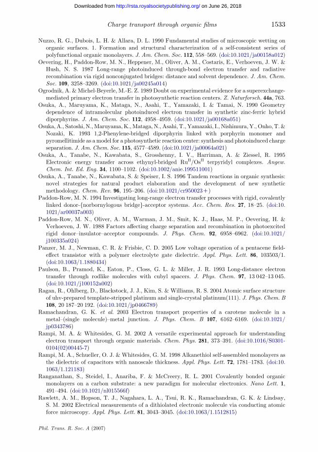
1533Charge transport through organic films
on June 26, 2018http://rsta.royalsocietypublishing.org/Downloaded from
Nuzzo, R. G., Dubois, L. H. & Allara, D. L. 1990 Fundamental studies of microscopic wetting on
organic surfaces. 1. Formation and structural characterization of a self-consistent series ofpolyfunctional organic monolayers. J. Am. Chem. Soc. 112, 558–569. (doi:10.1021/ja00158a012)
Oevering, H., Paddon-Row, M. N., Heppener, M., Oliver, A. M., Costaris, E., Verhoeven, J. W. &Hush, N. S. 1987 Long-range photoinduced through-bond electron transfer and radiativerecombination via rigid nonconjugated bridges: distance and solvent dependence. J. Am. Chem.
Soc. 109, 3258–3269. (doi:10.1021/ja00245a014)Ogrodnik, A. &Michel-Beyerle, M.-E. Z. 1989 Doubt on experimental evidence for a superexchange-
mediated primary electron transfer in photosynthetic reaction centers. Z. Naturforsch. 44a, 763.Osuka, A., Maruyama, K., Mataga, N., Asahi, T., Yamazaki, I. & Tamai, N. 1990 Geometry
dependence of intramolecular photoinduced electron transfer in synthetic zinc-ferric hybriddiporphyrins. J. Am. Chem. Soc. 112, 4958–4959. (doi:10.1021/ja00168a051)
Osuka, A., Satoshi, N.,Maruyama,K.,Mataga, N., Asahi, T., Yamazaki, I., Nishimura,Y., Onho, T.&Nozaki, K. 1993 1,2-Phenylene-bridged diporphyrin linked with porphyrin monomer and
pyromellitimide as amodel for a photosynthetic reaction center: synthesis and photoinduced chargeseparation. J. Am. Chem. Soc. 115, 4577–4589. (doi:10.1021/ja00064a021)
Osuka, A., Tanabe, N., Kawabata, S., Grosshenny, I. V., Harriman, A. & Ziessel, R. 1995Electronic energy transfer across ethynyl-bridged RuII/OsII terpyridyl complexes. Angew.Chem. Int. Ed. Eng. 34, 1100–1102. (doi:10.1002/anie.199511001)
Osuka, A., Tanabe, N., Kawabata, S. & Speiser, I. S. 1996 Tandem reactions in organic synthesis:novel strategies for natural product elaboration and the development of new synthetic
methodology. Chem. Rev. 96, 195–206. (doi:10.1021/cr950023C)Paddon-Row, M. N. 1994 Investigating long-range electron transfer processes with rigid, covalently
linked donor-{norbornylogous bridge}-acceptor systems. Acc. Chem. Res. 27, 18–25. (doi:10.1021/ar00037a003)
Paddon-Row, M. N., Oliver, A. M., Warman, J. M., Smit, K. J., Haas, M. P., Oevering, H. &Verhoeven, J. W. 1988 Factors affecting charge separation and recombination in photoexcitedrigid donor–insulator–acceptor compounds. J. Phys. Chem. 92, 6958–6962. (doi:10.1021/
j100335a024)Panzer, M. J., Newman, C. R. & Frisbie, C. D. 2005 Low voltage operation of a pentacene field-
effect transistor with a polymer electrolyte gate dielectric. Appl. Phys. Lett. 86, 103503/1.(doi:10.1063/1.1880434)
Paulson, B., Pramod, K., Eaton, P., Closs, G. L. & Miller, J. R. 1993 Long-distance electrontransfer through rodlike molecules with cubyl spacers. J. Phys. Chem. 97, 13 042–13 045.(doi:10.1021/j100152a002)
Ragan, R., Ohlberg, D., Blackstock, J. J., Kim, S. & Williams, R. S. 2004 Atomic surface structureof uhv-prepared template-stripped platinum and single-crystal platinum(111). J. Phys. Chem. B
108, 20 187–20 192. (doi:10.1021/jp0466789)Ramachandran, G. K. et al. 2003 Electron transport properties of a carotene molecule in a
metal–(single molecule)–metal junction. J. Phys. Chem. B 107, 6162–6169. (doi:10.1021/jp0343786)
Rampi, M. A. & Whitesides, G. M. 2002 A versatile experimental approach for understandingelectron transport through organic materials. Chem. Phys. 281, 373–391. (doi:10.1016/S0301-0104(02)00445-7)
Rampi, M. A., Schueller, O. J. & Whitesides, G. M. 1998 Alkanethiol self-assembled monolayers asthe dielectric of capacitors with nanoscale thickness. Appl. Phys. Lett. 72, 1781–1783. (doi:10.
1063/1.121183)Ranganathan, S., Steidel, I., Anariba, F. & McCreery, R. L. 2001 Covalently bonded organic
monolayers on a carbon substrate: a new paradigm for molecular electronics. Nano Lett. 1,491–494. (doi:10.1021/nl015566f)
Rawlett, A. M., Hopson, T. J., Nagahara, L. A., Tsui, R. K., Ramachandran, G. K. & Lindsay,S. M. 2002 Electrical measurements of a dithiolated electronic molecule via conducting atomicforce microscopy. Appl. Phys. Lett. 81, 3043–3045. (doi:10.1063/1.1512815)
Phil. Trans. R. Soc. A (2007)

E. A. Weiss et al.1534
on June 26, 2018http://rsta.royalsocietypublishing.org/Downloaded from
Reed, M. A., Zhou, C., Muller, C. J., Burgin, T. P. & Tour, J. M. 1997 Conductance of a molecular
junction. Science 278, 252–254. (doi:10.1126/science.278.5336.252)Reichert, J., Ochs, R., Beckmann, D., Weber, H. B., Mayor, M. & Lohneysen, H. V. 2002 Driving
current through single organic molecules. Phys. Rev. Lett. 88, 176 804. (doi:10.1103/PhysRevLett.88.176804)
Reimers, J. R., Shapely, W. A., Lambropoulos, N. & Hush, N. S. 2002 An atomistic approach to
conduction between nanoelectrodes through a single molecule. Ann. NY Acad. Sci. 960, 100.Reinerth, W. A., Jones, L., Burgin, T. P., Zhou, C., Muller, C. J., Deshpande, M. R., Reed, M. A.
& Tour, J. M. 1998 Molecular scale electronics: syntheses and testing. Nanotechnology 9,246–250. (doi:10.1088/0957-4484/9/3/016)
Roest, M. R., Oliver, A. M., Paddon-Row, M. N. & Verhoeven, J. W. 1997 Distance dependence ofsinglet and triplet charge recombination pathways in a series of rigid bichromophoric systems.
J. Phys. Chem. A 101, 4867–4871. (doi:10.1021/jp970969i)Rossetti, F. F., Reviakine, I. & Textor, M. 2003 Characterization of titanium oxide films by the
template-stripping method. Langmuir 19, 10 116–10 123. (doi:10.1021/la034280i)Sachs, S. B., Dudek, S. P., Hsung, R. P., Sita, L. R., Smalley, J. F., Newton, M. D., Feldberg, S. W.
& Chidsey, C. E. D. 1997 Rates of interfacial electron transfer through p-conjugated spacers.J. Am. Chem. Soc. 119, 10 563–10 564. (doi:10.1021/ja972244y)
Salomon, A., Berkovich, D. & Cahen, D. 2003 Molecular modification of an ionic semiconductor-metal interface: ZnO/molecule/Au didodes. Appl. Phys. Lett. 82, 1051–1053. (doi:10.1063/
1.1543638)Samori, P., Diebel, J., Loewe, H. & Rabe, J. P. 1999 Template stripped gold supported on Ni as a
substrate for SAMs. Langmuir 15, 2592–2594. (doi:10.1021/la981414x)Segal, D., Nitzan, A., Ratner, M. A. & Davis, W. B. 2000 Activated conduction in microscopic
molecular junctions. J. Phys. Chem. B 104, 2790–2793. (doi:10.1021/jp994296a)Segal, D., Nitzan, A. & Hanaggi, P. 2003 Thermal conductance through molecular wires. J. Chem.
Phys. 119, 6840–6855. (doi:10.1063/1.1603211)Seideman, T. & Guo, H. 2003 Quantum transport and current-triggered dynamics in molecular
tunnel junctions. J. Theor. Comp. Chem. 2, 439–458. (doi:10.1142/S0219633603000616)Sek, S., Bilewicz, R. & Slowinski, K. 2004 Electrochemical wiring of alkanedithiol molecules into an
electrical circuit. Chem. Commun. 404–405. (doi:10.1039/b314815g)Selzer, Y. & Cahen, D. 2001 Fine-tuning of Au/SiO2/Si diodes by varying interfacial dipoles using
molecular monolayers. Adv. Mater. 13, 508–511. (doi:10.1002/1521-4095(200104)13:7!508::AID-ADMA508O3.0.CO;2-8)
Selzer, Y., Salomon, A. & Cahen, D. 2002 Effect of molecule–metal electronic coupling on through-bond hole tunneling across metal-organic monolayer–semiconductor junctions. J. Am. Chem.
Soc. 124, 2886–2887. (doi:10.1021/ja0177511)Selzer, Y., Cabassi, M. A. & Mayer, T. S. 2004a Temperature effects on conduction through a
molecular junction. Nanotechnology 15, S483–S488. (doi:10.1088/0957-4484/15/7/057)Selzer, Y., Cabassi, M. A., Mayer, T. S. & Allara, D. L. 2004b Thermally activated conduction in
molecular junctions. J. Am. Chem. Soc. 126, 4052–4053. (doi:10.1021/ja039015y)Selzer, Y., Cai, L., Cabassi, M. A., Yao, Y., Tour, J. M., Mayer, T. S. & Allara, D. L. 2005 Effect of
local environment on molecular conduction: isolated molecule versus self-assembled monolayer.Nano Lett. 5, 61–65. (doi:10.1021/nl048372j)
Seminario, J. M. & Cordova, L. E. 2004 Theoretical interpretation of intrinsic line widths observed
in inelastic electron tunneling scattering experiments. J. Phys. Chem. A 108, 5142–5144.(doi:10.1021/jp048311C)
Service, R. F. 2003 Molecular electronics. Next-generation technology hits an early midlife crisis.Science 302, 556–559. (doi:10.1126/science.302.5645.556)
Shaheen, S. E., Ginley, D. S. & Jabbour, G. E. 2005 Organic-based photovoltaics: toward low costpower generation. MRS Bull. 30, 10.
Shankar, K. & Jackson, T. N. 2004 Morphology and electrical transport in pentacene films onsilylated oxide surfaces. J. Mater. Res. 19, 2003–2007. (doi:10.1557/JMR.2004.0255)
Phil. Trans. R. Soc. A (2007)
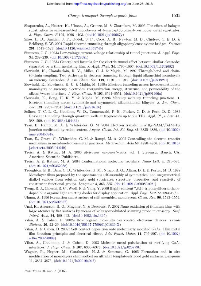
1535Charge transport through organic films
on June 26, 2018http://rsta.royalsocietypublishing.org/Downloaded from
Shaporenko, A., Heister, K., Ulman, A., Grunze, M. & Zharnikov, M. 2005 The effect of halogen
substitution in self-assembled monolayers of 4-mercaptobiphenyls on noble metal substrates.J. Phys. Chem. B 109, 4096–4103. (doi:10.1021/jp040667y)
Sikes, H. D., Smalley, J. F., Dudek, S. P., Cook, A. R., Newton, M. D., Chidsey, C. E. D. &Feldberg, S. W. 2001 Rapid electron tunneling through oligophenylenevinylene bridges. Science
291, 1519–1523. (doi:10.1126/science.1055745)Simmons, J. G. 1963a Low-voltage current-voltage relationship of tunnel junctions. J. Appl. Phys.
34, 238–239. (doi:10.1063/1.1729081)Simmons, J. G. 1963b Generalized formula for the electric tunnel effect between similar electrodes
separated by a thin insulating film. J. Appl. Phys. 34, 1793–1803. (doi:10.1063/1.1702682)Slowinski, K., Chamberlain, R. V., Miller, C. J. & Majda, M. 1997 Through-bond and chain-
to-chain coupling. Two pathways in electron tunneling through liquid alkanethiol monolayerson mercury electrodes. J. Am. Chem. Soc. 119, 11 910–11 919. (doi:10.1021/ja971921l)
Slowinski, K., Slowinska, K. U. & Majda, M. 1999a Electron tunneling across hexadecanethiolatemonolayers on mercury electrodes: reorganization energy, structure, and permeability of the
alkane/water interface. J. Phys. Chem. B 103, 8544–8551. (doi:10.1021/jp991466a)Slowinski, K., Fong, H. K. Y. & Majda, M. 1999b Mercury–mercury tunneling junctions. 1.
Electron tunneling across symmetric and asymmetric alkanethiolate bilayers. J. Am. Chem.Soc. 121, 7257–7261. (doi:10.1021/ja991613i)
Sollner, T. C. L. G., Goodhue, W. D., Tannenwald, P. E., Parker, C. D. & Peck, D. D. 1983Resonant tunneling through quantum wells at frequencies up to 2.5 THz. Appl. Phys. Lett. 43,
588–590. (doi:10.1063/1.94434)Tran, E., Rampi, M. A. & Whitesides, G. M. 2004 Electron transfer in a Hg–SAM//SAM–Hg
junction medicated by redox centers. Angew. Chem. Int. Ed. Eng. 43, 3835–3839. (doi:10.1002/anie.200453945)
Tran, E., Grave, C., Whitesides, G. M. & Rampi, M. A. 2005 Controlling the electron transfermechanism in metal-molecules-metal junctions. Electrochim. Acta 50, 4850–4856. (doi:10.1016/j.electacta.2005.04.049)
Troisi, A. & Ratner, M. A. 2003 Molecular nanoelectronics, vol. 1. Stevenson Ranch, CA:
American Scientific Publishers.Troisi, A. & Ratner, M. A. 2004 Conformational molecular rectifiers. Nano Lett. 4, 591–595.
(doi:10.1021/nl0352088)Troughton, E. B., Bain, C. D., Whitesides, G. M., Nuzzo, R. G., Allara, D. L. & Porter, M. D. 1988
Monolayer films prepared by the spontaneous self-assembly of symmetrical and unsymmetricaldialkyl sulfides from solution onto gold substrates: structure, properties, and reactivity ofconstituent functional groups. Langmuir 4, 365–385. (doi:10.1021/la00080a021)
Tseng, R. J., Chiechi, R. C.,Wudl, F. & Yang, Y. 2006 Highly efficient 7,8,10-triphenylfluoranthene-
doped blue organic light emitting diodes for display application. Appl. Phys. Lett. 88, 093512/1.Ulman, A. 1996 Formation and structure of self-assembled monolayers. Chem. Rev. 96, 1533–1554.
(doi:10.1021/cr9502357)Unal, K., Aronsson, B.-O., Mugnier, Y. & Descouts, P. 2002 Nano-oxidation of titanium films with
large atomically flat surfaces by means of voltage-modulated scanning probe microscopy. Surf.Interf. Anal. 34, 490–493. (doi:10.1002/sia.1345)
Vilan, A. & Cahen, D. 2002a How organic molecules can control electronic devices. TrendsBiotech. 20, 22–29. (doi:10.1016/S0167-7799(01)01839-X)
Vilan, A. & Cahen, D. 2002b Soft contact deposition onto molecularly modified GaAs. Thin metalfilm flotation: principles and electrical effects. Adv. Funct. Mater. 11, 795–807. (doi:10.1002/
adfm.200290009)Vilan, A., Ghabboun, J. & Cahen, D. 2003 Molecule–metal polarization at rectifying GaAs
interfaces. J. Phys. Chem. B 107, 6360–6376. (doi:10.1021/jp026779b)Wagner, P., Hegner, M., Guntherodt, H.-J. & Semenza, G. 1995 Formation and in situ
modification of monolayers chemisorbed on ultraflat template-stripped gold surfaces. Langmuir11, 3867–3875. (doi:10.1021/la00010a043)
Phil. Trans. R. Soc. A (2007)
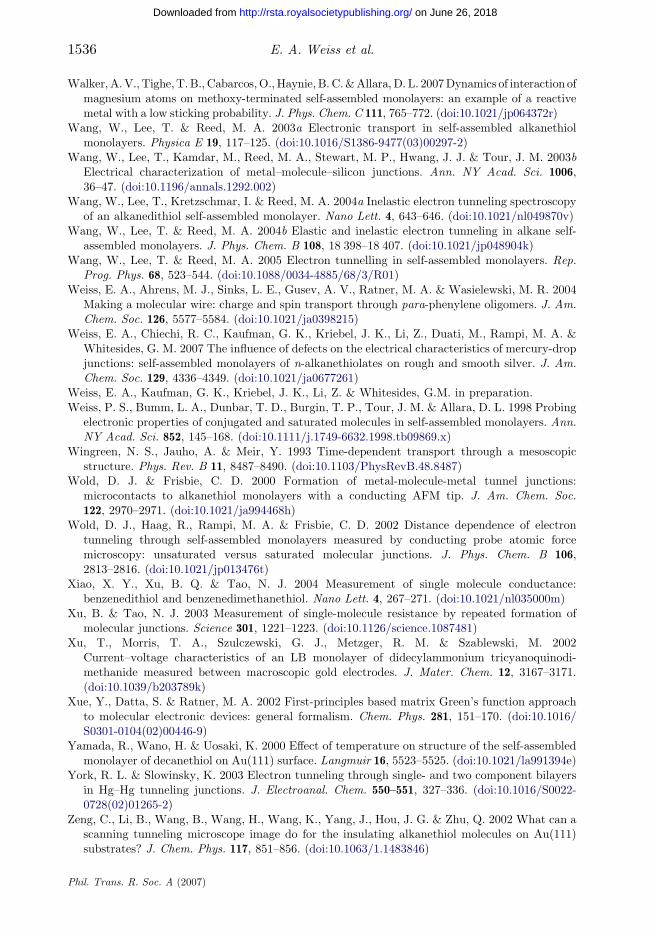
E. A. Weiss et al.1536
on June 26, 2018http://rsta.royalsocietypublishing.org/Downloaded from
Walker,A.V., Tighe,T.B., Cabarcos,O.,Haynie,B.C.&Allara,D. L. 2007Dynamics of interaction of
magnesium atoms on methoxy-terminated self-assembled monolayers: an example of a reactivemetal with a low sticking probability. J. Phys. Chem. C 111, 765–772. (doi:10.1021/jp064372r)
Wang, W., Lee, T. & Reed, M. A. 2003a Electronic transport in self-assembled alkanethiolmonolayers. Physica E 19, 117–125. (doi:10.1016/S1386-9477(03)00297-2)
Wang, W., Lee, T., Kamdar, M., Reed, M. A., Stewart, M. P., Hwang, J. J. & Tour, J. M. 2003bElectrical characterization of metal–molecule–silicon junctions. Ann. NY Acad. Sci. 1006,
36–47. (doi:10.1196/annals.1292.002)Wang, W., Lee, T., Kretzschmar, I. & Reed, M. A. 2004a Inelastic electron tunneling spectroscopy
of an alkanedithiol self-assembled monolayer. Nano Lett. 4, 643–646. (doi:10.1021/nl049870v)Wang, W., Lee, T. & Reed, M. A. 2004b Elastic and inelastic electron tunneling in alkane self-
assembled monolayers. J. Phys. Chem. B 108, 18 398–18 407. (doi:10.1021/jp048904k)Wang, W., Lee, T. & Reed, M. A. 2005 Electron tunnelling in self-assembled monolayers. Rep.
Prog. Phys. 68, 523–544. (doi:10.1088/0034-4885/68/3/R01)Weiss, E. A., Ahrens, M. J., Sinks, L. E., Gusev, A. V., Ratner, M. A. & Wasielewski, M. R. 2004
Making a molecular wire: charge and spin transport through para-phenylene oligomers. J. Am.Chem. Soc. 126, 5577–5584. (doi:10.1021/ja0398215)
Weiss, E. A., Chiechi, R. C., Kaufman, G. K., Kriebel, J. K., Li, Z., Duati, M., Rampi, M. A. &
Whitesides, G. M. 2007 The influence of defects on the electrical characteristics of mercury-dropjunctions: self-assembled monolayers of n-alkanethiolates on rough and smooth silver. J. Am.Chem. Soc. 129, 4336–4349. (doi:10.1021/ja0677261)
Weiss, E. A., Kaufman, G. K., Kriebel, J. K., Li, Z. & Whitesides, G.M. in preparation.Weiss, P. S., Bumm, L. A., Dunbar, T. D., Burgin, T. P., Tour, J. M. & Allara, D. L. 1998 Probing
electronic properties of conjugated and saturated molecules in self-assembled monolayers. Ann.NY Acad. Sci. 852, 145–168. (doi:10.1111/j.1749-6632.1998.tb09869.x)
Wingreen, N. S., Jauho, A. & Meir, Y. 1993 Time-dependent transport through a mesoscopic
structure. Phys. Rev. B 11, 8487–8490. (doi:10.1103/PhysRevB.48.8487)Wold, D. J. & Frisbie, C. D. 2000 Formation of metal-molecule-metal tunnel junctions:
microcontacts to alkanethiol monolayers with a conducting AFM tip. J. Am. Chem. Soc.122, 2970–2971. (doi:10.1021/ja994468h)
Wold, D. J., Haag, R., Rampi, M. A. & Frisbie, C. D. 2002 Distance dependence of electrontunneling through self-assembled monolayers measured by conducting probe atomic forcemicroscopy: unsaturated versus saturated molecular junctions. J. Phys. Chem. B 106,
2813–2816. (doi:10.1021/jp013476t)Xiao, X. Y., Xu, B. Q. & Tao, N. J. 2004 Measurement of single molecule conductance:
benzenedithiol and benzenedimethanethiol. Nano Lett. 4, 267–271. (doi:10.1021/nl035000m)Xu, B. & Tao, N. J. 2003 Measurement of single-molecule resistance by repeated formation of
molecular junctions. Science 301, 1221–1223. (doi:10.1126/science.1087481)Xu, T., Morris, T. A., Szulczewski, G. J., Metzger, R. M. & Szablewski, M. 2002
Current–voltage characteristics of an LB monolayer of didecylammonium tricyanoquinodi-methanide measured between macroscopic gold electrodes. J. Mater. Chem. 12, 3167–3171.
(doi:10.1039/b203789k)Xue, Y., Datta, S. & Ratner, M. A. 2002 First-principles based matrix Green’s function approach
to molecular electronic devices: general formalism. Chem. Phys. 281, 151–170. (doi:10.1016/S0301-0104(02)00446-9)
Yamada, R., Wano, H. & Uosaki, K. 2000 Effect of temperature on structure of the self-assembledmonolayer of decanethiol on Au(111) surface. Langmuir 16, 5523–5525. (doi:10.1021/la991394e)
York, R. L. & Slowinsky, K. 2003 Electron tunneling through single- and two component bilayersin Hg–Hg tunneling junctions. J. Electroanal. Chem. 550–551, 327–336. (doi:10.1016/S0022-
0728(02)01265-2)Zeng, C., Li, B., Wang, B., Wang, H., Wang, K., Yang, J., Hou, J. G. & Zhu, Q. 2002 What can a
scanning tunneling microscope image do for the insulating alkanethiol molecules on Au(111)substrates? J. Chem. Phys. 117, 851–856. (doi:10.1063/1.1483846)
Phil. Trans. R. Soc. A (2007)

1537Charge transport through organic films
on June 26, 2018http://rsta.royalsocietypublishing.org/Downloaded from
Zhou, C., Deshpande, M. R., Reed, M. A., Jones, L. & Tour, J. M. 1997 Nanoscale metal/self-assembled monolayer/metal heterostructures. Appl. Phys. Lett. 71, 611–613. (doi:10.1063/1.120195)
Zhou, D., Bruckbauer, A., Batchelor, M., LKang, D.-J., Abell, C. & LKlenerman, D. 2004 Theinfluence of the foundation layer on the layer-by-layer assembly of poly-L-lysine andpolystyrenesulfonate and its usage in the fabrication of 3D microscale features. Langmuir 20,9089–9094. (doi:10.1021/la048619s)
Zhu, Z., Daniel, T. A., Maitani, M., Cabarcos, O. & Allara, D. L. 2006 Controlling gold atompenetration through alkanethiolate self-assembled monolayers on Au{111} by adjustingterminal group intermolecular interactions. J. Am. Chem. Soc. 128, 13 710–13 719. (doi:10.1021/ja060084x)
Phil. Trans. R. Soc. A (2007)


