The Scientist and Engineer's Guide to Digital Signal ...
32
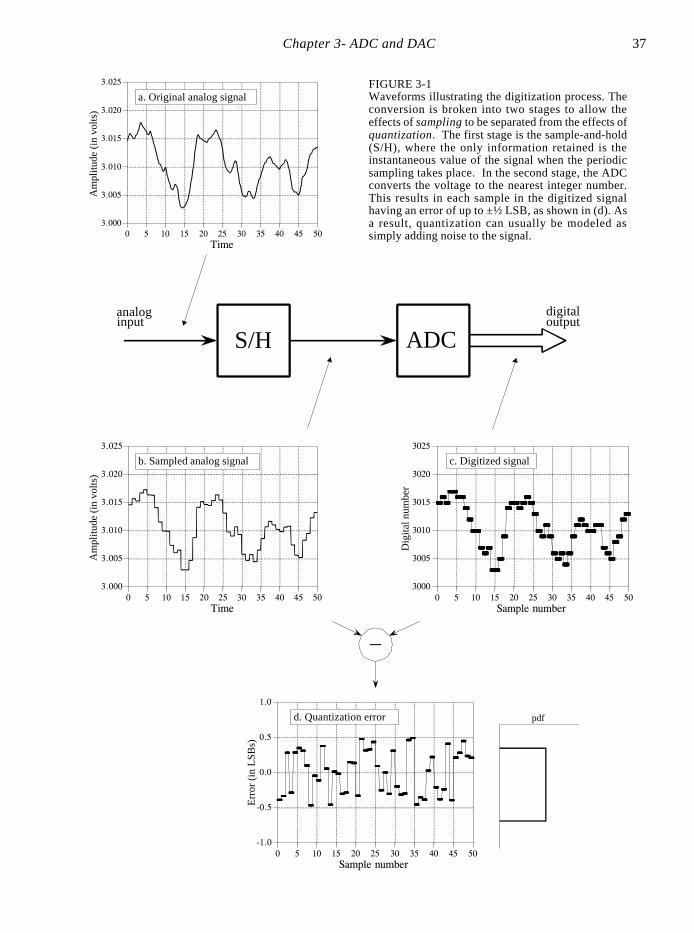
35 CHAPTER 3 ADC and DAC Most of the signals directly encountered in science and engineering are continuous: light intensity that changes with distance; voltage that varies over time; a chemical reaction rate that depends on temperature, etc. Analog-to-Digital Conversion (ADC) and Digital-to-Analog Conversion (DAC) are the processes that allow digital computers to interact with these everyday signals. Digital information is different from its continuous counterpart in two important respects: it is sampled, and it is quantized. Both of these restrict how much information a digital signal can contain. This chapter is about information management : understanding what information you need to retain, and what information you can afford to lose. In turn, this dictates the selection of the sampling frequency, number of bits, and type of analog filtering needed for converting between the analog and digital realms. Quantization First, a bit of trivia. As you know, it is a digital computer, not a digit computer. The information processed is called digital data, not digit data. Why then, is analog-to-digital conversion generally called: digit ize and digit ization, rather than digital ize and digital ization? The answer is nothing you would expect. When electronics got around to inventing digital techniques, the preferred names had already been snatched up by the medical community nearly a century before. Digitalize and digitalization mean to administer the heart stimulant digitalis. Figure 3-1 shows the electronic waveforms of a typical analog-to-digital conversion. Figure (a) is the analog signal to be digitized. As shown by the labels on the graph, this signal is a voltage that varies over time . To make the numbers easier, we will assume that the voltage can vary from 0 to 4.095 volts, corresponding to the digital numbers between 0 and 4095 that will be produced by a 12 bit digitizer. Notice that the block diagram is broken into two sections, the sample-and-hold (S/H), and the analog-to-digital converter (ADC). As you probably learned in electronics classes, the sample-and-hold is required to keep the voltage entering the ADC constant while the
Transcript of The Scientist and Engineer's Guide to Digital Signal ...
35
CHAPTER
3ADC and DAC
Most of the signals directly encountered in science and engineering are continuous: light intensitythat changes with distance; voltage that varies over time; a chemical reaction rate that dependson temperature, etc. Analog-to-Digital Conversion (ADC) and Digital-to-Analog Conversion(DAC) are the processes that allow digital computers to interact with these everyday signals.Digital information is different from its continuous counterpart in two important respects: it issampled, and it is quantized. Both of these restrict how much information a digital signal cancontain. This chapter is about information management: understanding what information youneed to retain, and what information you can afford to lose. In turn, this dictates the selectionof the sampling frequency, number of bits, and type of analog filtering needed for convertingbetween the analog and digital realms.
Quantization
First, a bit of trivia. As you know, it is a digital computer, not a digitcomputer. The information processed is called digital data, not digit data.Why then, is analog-to-digital conversion generally called: digitize anddigitization, rather than digitalize and digitalization? The answer is nothingyou would expect. When electronics got around to inventing digital techniques,the preferred names had already been snatched up by the medical communitynearly a century before. Digitalize and digitalization mean to administer theheart stimulant digitalis.
Figure 3-1 shows the electronic waveforms of a typical analog-to-digitalconversion. Figure (a) is the analog signal to be digitized. As shown by thelabels on the graph, this signal is a voltage that varies over time. To makethe numbers easier, we will assume that the voltage can vary from 0 to 4.095volts, corresponding to the digital numbers between 0 and 4095 that will beproduced by a 12 bit digitizer. Notice that the block diagram is broken intotwo sections, the sample-and-hold (S/H), and the analog-to-digital converter(ADC). As you probably learned in electronics classes, the sample-and-holdis required to keep the voltage entering the ADC constant while the
The Scientist and Engineer's Guide to Digital Signal Processing36
conversion is taking place. However, this is not the reason it is shown here;breaking the digitization into these two stages is an important theoretical modelfor understanding digitization. The fact that it happens to look like commonelectronics is just a fortunate bonus.
As shown by the difference between (a) and (b), the output of the sample-and-hold is allowed to change only at periodic intervals, at which time it is madeidentical to the instantaneous value of the input signal. Changes in the inputsignal that occur between these sampling times are completely ignored. Thatis, sampling converts the independent variable (time in this example) fromcontinuous to discrete.
As shown by the difference between (b) and (c), the ADC produces an integervalue between 0 and 4095 for each of the flat regions in (b). This introducesan error, since each plateau can be any voltage between 0 and 4.095 volts. Forexample, both 2.56000 volts and 2.56001 volts will be converted into digitalnumber 2560. In other words, quantization converts the dependent variable(voltage in this example) from continuous to discrete.
Notice that we carefully avoid comparing (a) and (c), as this would lump thesampling and quantization together. It is important that we analyze themseparately because they degrade the signal in different ways, as well as beingcontrolled by different parameters in the electronics. There are also caseswhere one is used without the other. For instance, sampling withoutquantization is used in switched capacitor filters.
First we will look at the effects of quantization. Any one sample in thedigitized signal can have a maximum error of ±½ LSB (Least SignificantBit, jargon for the distance between adjacent quantization levels). Figure (d)shows the quantization error for this particular example, found by subtracting(b) from (c), with the appropriate conversions. In other words, the digitaloutput (c), is equivalent to the continuous input (b), plus a quantization error(d). An important feature of this analysis is that the quantization error appearsvery much like random noise.
This sets the stage for an important model of quantization error. In most cases,quantization results in nothing more than the addition of a specific amountof random noise to the signal. The additive noise is uniformly distributedbetween ±½ LSB, has a mean of zero, and a standard deviation of LSB1/ 12(-0.29 LSB). For example, passing an analog signal through an 8 bit digitizeradds an rms noise of: , or about 1/900 of the full scale value. A 120.29 /256bit conversion adds a noise of: , while a 16 bit0.29 /4096 . 1 /14,000conversion adds: . Since quantization error is a0.29 /65536 . 1 /227,000random noise, the number of bits determines the precision of the data. Forexample, you might make the statement: "We increased the precision of themeasurement from 8 to 12 bits."
This model is extremely powerful, because the random noise generated byquantization will simply add to whatever noise is already present in the
Chapter 3- ADC and DAC 37
Time0 5 10 15 20 25 30 35 40 45 50
3.000
3.005
3.010
3.015
3.020
3.025
a. Original analog signal
Time0 5 10 15 20 25 30 35 40 45 50
3.000
3.005
3.010
3.015
3.020
3.025
b. Sampled analog signal
Sample number0 5 10 15 20 25 30 35 40 45 50
3000
3005
3010
3015
3020
3025
c. Digitized signal
Sample number0 5 10 15 20 25 30 35 40 45 50
-1.0
-0.5
0.0
0.5
1.0
d. Quantization error
analoginput
digitaloutput
S/H ADC
FIGURE 3-1Waveforms illustrating the digitization process. Theconversion is broken into two stages to allow theeffects of sampling to be separated from the effects ofquantization. The first stage is the sample-and-hold(S/H), where the only information retained is theinstantaneous value of the signal when the periodicsampling takes place. In the second stage, the ADCconverts the voltage to the nearest integer number.This results in each sample in the digitized signalhaving an error of up to ±½ LSB, as shown in (d). Asa result, quantization can usually be modeled assimply adding noise to the signal.
Am
plitu
de (
in v
olts
)A
mpl
itude
(in
vol
ts)
Dig
ital n
umbe
r
Err
or (
in L
SBs)

The Scientist and Engineer's Guide to Digital Signal Processing38
analog signal. For example, imagine an analog signal with a maximumamplitude of 1.0 volt, and a random noise of 1.0 millivolt rms. Digitizing thissignal to 8 bits results in 1.0 volt becoming digital number 255, and 1.0millivolt becoming 0.255 LSB. As discussed in the last chapter, random noisesignals are combined by adding their variances. That is, the signals are addedin quadrature: . The total noise on the digitized signal isA 2%B 2 ' Ctherefore given by: LSB. This is an increase of about0.2552 % 0.292 ' 0.38650% over the noise already in the analog signal. Digitizing this same signalto 12 bits would produce virtually no increase in the noise, and nothing wouldbe lost due to quantization. When faced with the decision of how many bitsare needed in a system, ask two questions: (1) How much noise is alreadypresent in the analog signal? (2) How much noise can be tolerated in thedigital signal?
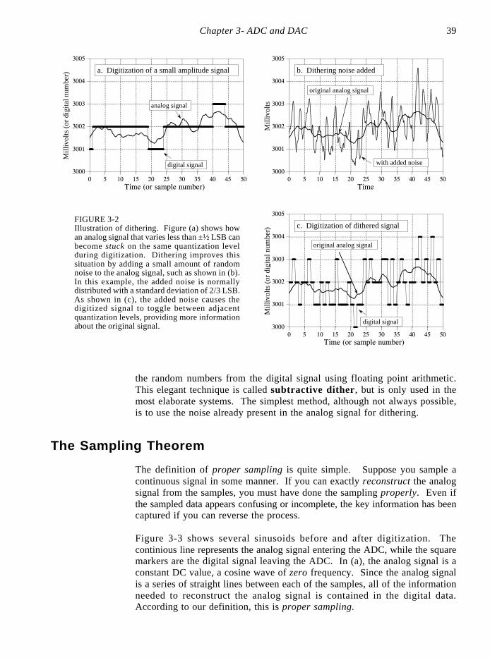
When isn't this model of quantization valid? Only when the quantizationerror cannot be treated as random. The only common occurrence of thisis when the analog signal remains at about the same value for manyconsecutive samples, as is illustrated in Fig. 3-2a. The output remainsstuck on the same digital number for many samples in a row, even thoughthe analog signal may be changing up to ±½ LSB. Instead of being anadditive random noise, the quantization error now looks like a thresholdingeffect or weird distortion.
Dithering is a common technique for improving the digitization of theseslowly varying signals. As shown in Fig. 3-2b, a small amount of randomnoise is added to the analog signal. In this example, the added noise isnormally distributed with a standard deviation of 2/3 LSB, resulting in a peak-to-peak amplitude of about 3 LSB. Figure (c) shows how the addition of thisdithering noise has affected the digitized signal. Even when the original analogsignal is changing by less than ±½ LSB, the added noise causes the digitaloutput to randomly toggle between adjacent levels.
To understand how this improves the situation, imagine that the input signalis a constant analog voltage of 3.0001 volts, making it one-tenth of the waybetween the digital levels 3000 and 3001. Without dithering, taking10,000 samples of this signal would produce 10,000 identical numbers, allhaving the value of 3000. Next, repeat the thought experiment with a smallamount of dithering noise added. The 10,000 values will now oscillatebetween two (or more) levels, with about 90% having a value of 3000, and10% having a value of 3001. Taking the average of all 10,000 valuesresults in something close to 3000.1. Even though a single measurementhas the inherent ±½ LSB limitation, the statistics of a large number of thesamples can do much better. This is quite a strange situation: addingnoise provides more information.
Circuits for dithering can be quite sophisticated, such as using a computerto generate random numbers, and then passing them through a DAC toproduce the added noise. After digitization, the computer can subtract
Chapter 3- ADC and DAC 39
Time (or sample number)0 5 10 15 20 25 30 35 40 45 50
3000
3001
3002
3003
3004
3005
original analog signal
digital signal
c. Digitization of dithered signal
Time (or sample number)0 5 10 15 20 25 30 35 40 45 50
3000
3001
3002
3003
3004
3005
a. Digitization of a small amplitude signal
analog signal
digital signal
Time0 5 10 15 20 25 30 35 40 45 50
3000
3001
3002
3003
3004
3005
original analog signal
with added noise
b. Dithering noise added
Mill
ivol
ts (
or d
igita
l num
ber)
Mill
ivol
ts
Mill
ivol
ts (
or d
igita
l num
ber)
FIGURE 3-2Illustration of dithering. Figure (a) shows howan analog signal that varies less than ±½ LSB canbecome stuck on the same quantization levelduring digitization. Dithering improves thissituation by adding a small amount of randomnoise to the analog signal, such as shown in (b).In this example, the added noise is normallydistributed with a standard deviation of 2/3 LSB.As shown in (c), the added noise causes thedigitized signal to toggle between adjacentquantization levels, providing more informationabout the original signal.
the random numbers from the digital signal using floating point arithmetic.This elegant technique is called subtractive dither, but is only used in themost elaborate systems. The simplest method, although not always possible,is to use the noise already present in the analog signal for dithering.
The Sampling Theorem
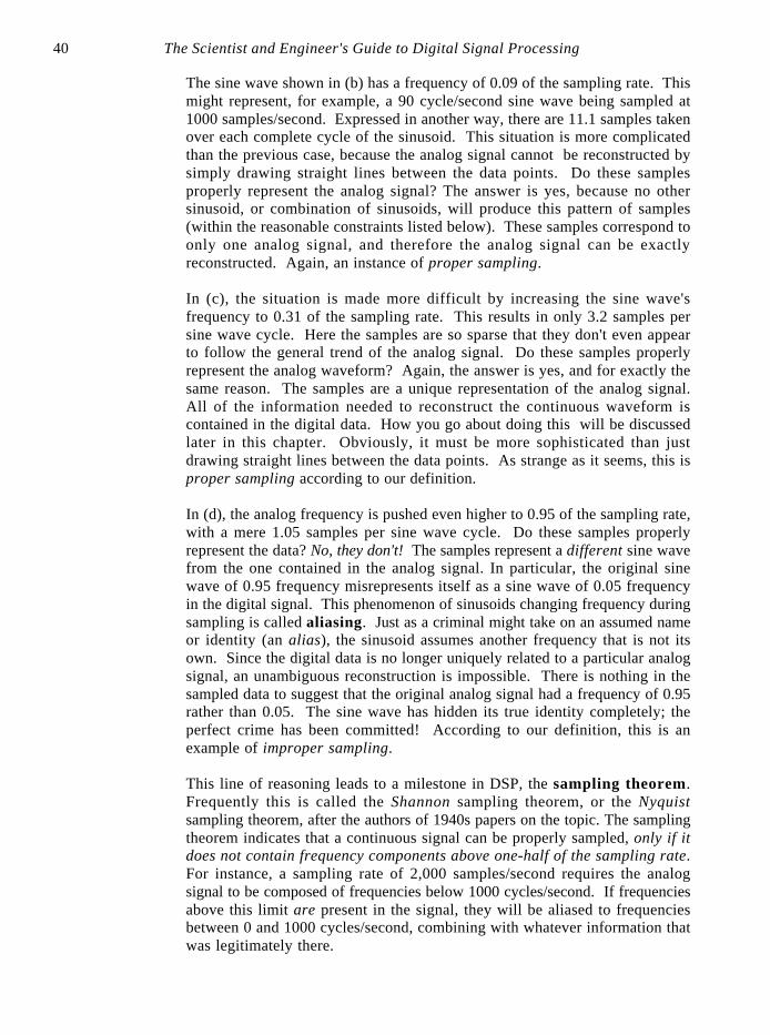
The definition of proper sampling is quite simple. Suppose you sample acontinuous signal in some manner. If you can exactly reconstruct the analogsignal from the samples, you must have done the sampling properly. Even ifthe sampled data appears confusing or incomplete, the key information has beencaptured if you can reverse the process.
Figure 3-3 shows several sinusoids before and after digitization. Thecontinious line represents the analog signal entering the ADC, while the squaremarkers are the digital signal leaving the ADC. In (a), the analog signal is aconstant DC value, a cosine wave of zero frequency. Since the analog signalis a series of straight lines between each of the samples, all of the informationneeded to reconstruct the analog signal is contained in the digital data.According to our definition, this is proper sampling.
The Scientist and Engineer's Guide to Digital Signal Processing40
The sine wave shown in (b) has a frequency of 0.09 of the sampling rate. Thismight represent, for example, a 90 cycle/second sine wave being sampled at1000 samples/second. Expressed in another way, there are 11.1 samples takenover each complete cycle of the sinusoid. This situation is more complicatedthan the previous case, because the analog signal cannot be reconstructed bysimply drawing straight lines between the data points. Do these samplesproperly represent the analog signal? The answer is yes, because no othersinusoid, or combination of sinusoids, will produce this pattern of samples(within the reasonable constraints listed below). These samples correspond toonly one analog signal, and therefore the analog signal can be exactlyreconstructed. Again, an instance of proper sampling.
In (c), the situation is made more difficult by increasing the sine wave'sfrequency to 0.31 of the sampling rate. This results in only 3.2 samples persine wave cycle. Here the samples are so sparse that they don't even appearto follow the general trend of the analog signal. Do these samples properlyrepresent the analog waveform? Again, the answer is yes, and for exactly thesame reason. The samples are a unique representation of the analog signal.All of the information needed to reconstruct the continuous waveform iscontained in the digital data. How you go about doing this will be discussedlater in this chapter. Obviously, it must be more sophisticated than justdrawing straight lines between the data points. As strange as it seems, this isproper sampling according to our definition.
In (d), the analog frequency is pushed even higher to 0.95 of the sampling rate,with a mere 1.05 samples per sine wave cycle. Do these samples properlyrepresent the data? No, they don't! The samples represent a different sine wavefrom the one contained in the analog signal. In particular, the original sinewave of 0.95 frequency misrepresents itself as a sine wave of 0.05 frequencyin the digital signal. This phenomenon of sinusoids changing frequency duringsampling is called aliasing. Just as a criminal might take on an assumed nameor identity (an alias), the sinusoid assumes another frequency that is not itsown. Since the digital data is no longer uniquely related to a particular analogsignal, an unambiguous reconstruction is impossible. There is nothing in thesampled data to suggest that the original analog signal had a frequency of 0.95rather than 0.05. The sine wave has hidden its true identity completely; theperfect crime has been committed! According to our definition, this is anexample of improper sampling.
This line of reasoning leads to a milestone in DSP, the sampling theorem.Frequently this is called the Shannon sampling theorem, or the Nyquistsampling theorem, after the authors of 1940s papers on the topic. The samplingtheorem indicates that a continuous signal can be properly sampled, only if itdoes not contain frequency components above one-half of the sampling rate.For instance, a sampling rate of 2,000 samples/second requires the analogsignal to be composed of frequencies below 1000 cycles/second. If frequenciesabove this limit are present in the signal, they will be aliased to frequenciesbetween 0 and 1000 cycles/second, combining with whatever information thatwas legitimately there.
Chapter 3- ADC and DAC 41
Time (or sample number)-3
-2
-1
0
1
2
3
c. Analog frequency = 0.31 of sampling rate
Time (or sample number)-3
-2
-1
0
1
2
3
d. Analog frequency = 0.95 of sampling rate
Time (or sample number)-3
-2
-1
0
1
2
3
a. Analog frequency = 0.0 (i.e., DC)
Time (or sample number)-3
-2
-1
0
1
2
3
b. Analog frequency = 0.09 of sampling rate
Am
plitu
deA
mpl
itude
Am
plitu
de
FIGURE 3-3Illustration of proper and improper sampling. A continuous signal is sampled properly if the samples contain all theinformation needed to recreated the original waveform. Figures (a), (b), and (c) illustrate proper sampling of threesinusoidal waves. This is certainly not obvious, since the samples in (c) do not even appear to capture the shape of thewaveform. Nevertheless, each of these continuous signals forms a unique one-to-one pair with its pattern of samples.This guarantees that reconstruction can take place. In (d), the frequency of the analog sine wave is greater than theNyquist frequency (one-half of the sampling rate). This results in aliasing, where the frequency of the sampled data isdifferent from the frequency of the continuous signal. Since aliasing has corrupted the information, the original signalcannot be reconstructed from the samples.
Am
plitu
de
Two terms are widely used when discussing the sampling theorem: theNyquist frequency and the Nyquist rate. Unfortunately, their meaning isnot standardized. To understand this, consider an analog signal composed offrequencies between DC and 3 kHz. To properly digitize this signal it mustbe sampled at 6,000 samples/sec (6 kHz) or higher. Suppose we choose tosample at 8,000 samples/sec (8 kHz), allowing frequencies between DC and 4kHz to be properly represented. In this situation their are four importantfrequencies: (1) the highest frequency in the signal, 3 kHz; (2) twice thisfrequency, 6 kHz; (3) the sampling rate, 8 kHz; and (4) one-half the samplingrate, 4 kHz. Which of these four is the Nyquist frequency and which is theNyquist rate? It depends who you ask! All of the possible combinations are
The Scientist and Engineer's Guide to Digital Signal Processing42
used. Fortunately, most authors are careful to define how they are using theterms. In this book, they are both used to mean one-half the sampling rate.
Figure 3-4 shows how frequencies are changed during aliasing. The keypoint to remember is that a digital signal cannot contain frequencies aboveone-half the sampling rate (i.e., the Nyquist frequency/rate). When thefrequency of the continuous wave is below the Nyquist rate, the frequencyof the sampled data is a match. However, when the continuous signal'sfrequency is above the Nyquist rate, aliasing changes the frequency intosomething that can be represented in the sampled data. As shown by thezigzagging line in Fig. 3-4, every continuous frequency above the Nyquistrate has a corresponding digital frequency between zero and one-half thesampling rate. If there happens to be a sinusoid already at this lowerfrequency, the aliased signal will add to it , resulting in a loss ofinformation. Aliasing is a double curse; information can be lost about thehigher and the lower frequency. Suppose you are given a digital signalcontaining a frequency of 0.2 of the sampling rate. If this signal wereobtained by proper sampling, the original analog signal must have had afrequency of 0.2. If aliasing took place during sampling, the digitalfrequency of 0.2 could have come from any one of an infinite number offrequencies in the analog signal: 0.2, 0.8, 1.2, 1.8, 2.2, þ .
Just as aliasing can change the frequency during sampling, it can also changethe phase. For example, look back at the aliased signal in Fig. 3-3d. Thealiased digital signal is inverted from the original analog signal; one is a sinewave while the other is a negative sine wave. In other words, aliasing haschanged the frequency and introduced a 180E phase shift. Only two phaseshifts are possible: 0E (no phase shift) and 180E (inversion). The zero phaseshift occurs for analog frequencies of 0 to 0.5, 1.0 to 1.5, 2.0 to 2.5, etc. Aninverted phase occurs for analog frequencies of 0.5 to 1.0, 1.5 to 2.0, 2.5 to3.0, and so on.
Now we will dive into a more detailed analysis of sampling and how aliasingoccurs. Our overall goal is to understand what happens to the informationwhen a signal is converted from a continuous to a discrete form. The problemis, these are very different things; one is a continuous waveform while theother is an array of numbers. This "apples-to-oranges" comparison makes theanalysis very difficult. The solution is to introduce a theoretical concept calledthe impulse train.
Figure 3-5a shows an example analog signal. Figure (c) shows the signalsampled by using an impulse train. The impulse train is a continuous signalconsisting of a series of narrow spikes (impulses) that match the original signalat the sampling instants. Each impulse is infinitesimally narrow, a concept thatwill be discussed in Chapter 13. Between these sampling times the value of thewaveform is zero. Keep in mind that the impulse train is a theoretical concept,not a waveform that can exist in an electronic circuit. Since both the originalanalog signal and the impulse train are continuous waveforms, we can make an"apples-apples" comparison between the two.

Chapter 3- ADC and DAC 43
Continuous frequency (as a fraction of the sampling rate)0.0 0.5 1.0 1.5 2.0 2.5
0.0
0.1
0.2
0.3
0.4
0.5
DCNyquist
Frequency
GOODALIASED
FIGURE 3-4Conversion of analog frequency into digital frequency during sampling. Continuous signals witha frequency less than one-half of the sampling rate are directly converted into the correspondingdigital frequency. Above one-half of the sampling rate, aliasing takes place, resulting in the frequencybeing misrepresented in the digital data. Aliasing always changes a higher frequency into a lowerfrequency between 0 and 0.5. In addition, aliasing may also change the phase of the signal by 180degrees.
Continuous frequency (as a fraction of the sampling rate)0.0 0.5 1.0 1.5 2.0 2.5
-90
0
90
180
270
Dig
ital f
requ
ency
Dig
ital p
hase
(de
gree
s)
Now we need to examine the relationship between the impulse train and thediscrete signal (an array of numbers). This one is easy; in terms of informationcontent, they are identical. If one is known, it is trivial to calculate the other.Think of these as different ends of a bridge crossing between the analog anddigital worlds. This means we have achieved our overall goal once weunderstand the consequences of changing the waveform in Fig. 3-5a into thewaveform in Fig. 3.5c.
Three continuous waveforms are shown in the left-hand column in Fig. 3-5. Thecorresponding frequency spectra of these signals are displayed in the right-hand column. This should be a familiar concept from your knowledge ofelectronics; every waveform can be viewed as being composed of sinusoids ofvarying amplitude and frequency. Later chapters will discuss the frequencydomain in detail. (You may want to revisit this discussion after becoming morefamiliar with frequency spectra).
Figure (a) shows an analog signal we wish to sample. As indicated by itsfrequency spectrum in (b), it is composed only of frequency componentsbetween 0 and about 0.33 fs, where fs is the sampling frequency we intend to
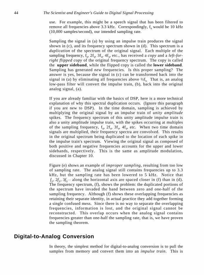
The Scientist and Engineer's Guide to Digital Signal Processing44
use. For example, this might be a speech signal that has been filtered toremove all frequencies above 3.3 kHz. Correspondingly, fs would be 10 kHz(10,000 samples/second), our intended sampling rate.
Sampling the signal in (a) by using an impulse train produces the signalshown in (c), and its frequency spectrum shown in (d). This spectrum is aduplication of the spectrum of the original signal. Each multiple of thesampling frequency, fs, 2fs, 3fs, 4fs, etc., has received a copy and a left-for-right flipped copy of the original frequency spectrum. The copy is calledthe upper sideband, while the flipped copy is called the lower sideband.Sampling has generated new frequencies. Is this proper sampling? Theanswer is yes, because the signal in (c) can be transformed back into thesignal in (a) by eliminating all frequencies above ½fs. That is, an analoglow-pass filter will convert the impulse train, (b), back into the originalanalog signal, (a).
If you are already familiar with the basics of DSP, here is a more technicalexplanation of why this spectral duplication occurs. (Ignore this paragraphif you are new to DSP). In the time domain, sampling is achieved bymultiplying the original signal by an impulse train of unity amplitudespikes. The frequency spectrum of this unity amplitude impulse train isalso a unity amplitude impulse train, with the spikes occurring at multiplesof the sampling frequency, fs, 2fs, 3fs, 4fs, etc. When two time domainsignals are multiplied, their frequency spectra are convolved. This resultsin the original spectrum being duplicated to the location of each spike inthe impulse train's spectrum. Viewing the original signal as composed ofboth positive and negative frequencies accounts for the upper and lowersidebands, respectively. This is the same as amplitude modulation,discussed in Chapter 10.
Figure (e) shows an example of improper sampling, resulting from too lowof sampling rate. The analog signal still contains frequencies up to 3.3kHz, but the sampling rate has been lowered to 5 kHz. Notice that
along the horizontal axis are spaced closer in (f) than in (d).fS , 2fS , 3fS þThe frequency spectrum, (f), shows the problem: the duplicated portions ofthe spectrum have invaded the band between zero and one-half of thesampling frequency. Although (f) shows these overlapping frequencies asretaining their separate identity, in actual practice they add together forminga single confused mess. Since there is no way to separate the overlappingfrequencies, information is lost, and the original signal cannot bereconstructed. This overlap occurs when the analog signal containsfrequencies greater than one-half the sampling rate, that is, we have proventhe sampling theorem.
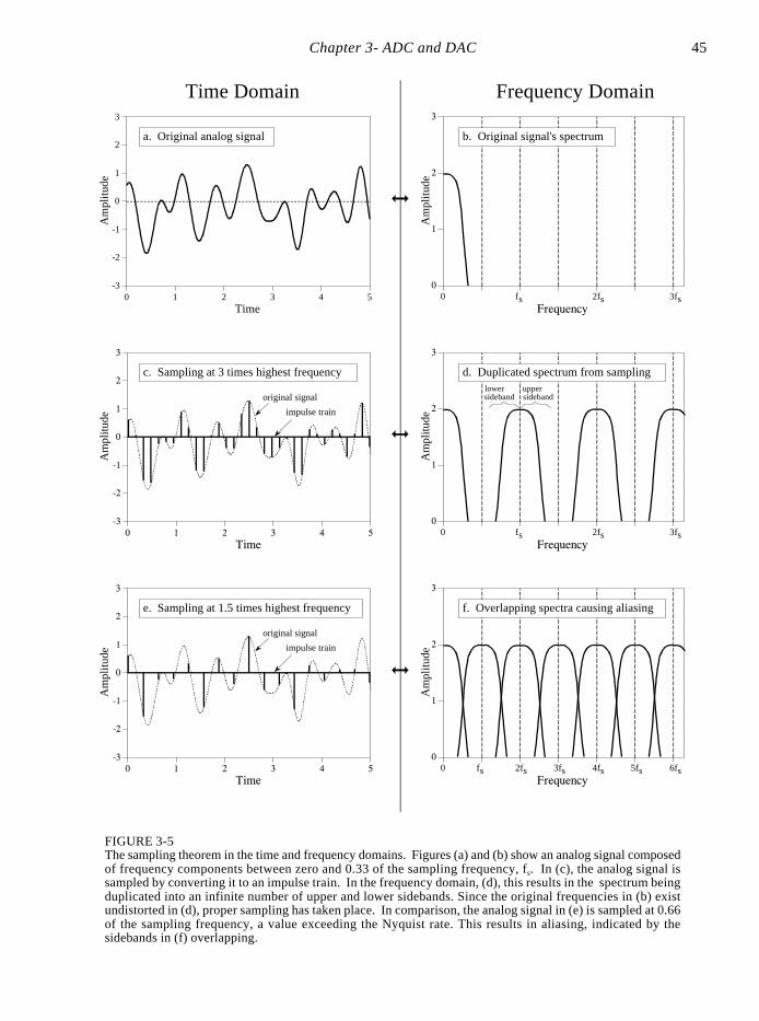
Digital-to-Analog Conversion
In theory, the simplest method for digital-to-analog conversion is to pull thesamples from memory and convert them into an impulse train. This is
Chapter 3- ADC and DAC 45
Time0 1 2 3 4 5
-3
-2
-1
0
1
2
3
a. Original analog signal
Frequency0 100 200 300 400 500 600
0
1
2
3
b. Original signal's spectrum
0 f 2f 3fsss
Time0 1 2 3 4 5
-3
-2
-1
0
1
2
3
original signal
impulse train
c. Sampling at 3 times highest frequency
Frequency0 100 200 300 400 500 600
0
1
2
3
d. Duplicated spectrum from samplingupper
sidebandlower
sideband
0 f 2f 3fsss
Time0 1 2 3 4 5
-3
-2
-1
0
1
2
3
e. Sampling at 1.5 times highest frequency
original signal
impulse train
Frequency0 100 200 300 400 500 600
0
1
2
3
f. Overlapping spectra causing aliasing
0 2f 4f 6fsssfs 3f 5fss
Time Domain Frequency Domain
FIGURE 3-5The sampling theorem in the time and frequency domains. Figures (a) and (b) show an analog signal composedof frequency components between zero and 0.33 of the sampling frequency, fs. In (c), the analog signal issampled by converting it to an impulse train. In the frequency domain, (d), this results in the spectrum beingduplicated into an infinite number of upper and lower sidebands. Since the original frequencies in (b) existundistorted in (d), proper sampling has taken place. In comparison, the analog signal in (e) is sampled at 0.66of the sampling frequency, a value exceeding the Nyquist rate. This results in aliasing, indicated by thesidebands in (f) overlapping.
Am
plitu
de
Am
plitu
de
Am
plitu
de
Am
plitu
deA
mpl
itude
Am
plitu
de
The Scientist and Engineer's Guide to Digital Signal Processing46
EQUATION 3-1High frequency amplitude reduction due tothe zeroth-order hold. This curve is plottedin Fig. 3-6d. The sampling frequency isrepresented by . For .fS f ' 0, H ( f ) ' 1
H ( f ) ' /00sin(Bf /fs )
Bf /fs/00
illustrated in Fig. 3-6a, with the corresponding frequency spectrum in (b). Asjust described, the original analog signal can be perfectly reconstructed bypassing this impulse train through a low-pass filter, with the cutoff frequencyequal to one-half of the sampling rate. In other words, the original signal andthe impulse train have identical frequency spectra below the Nyquist frequency(one-half the sampling rate). At higher frequencies, the impulse train containsa duplication of this information, while the original analog signal containsnothing (assuming aliasing did not occur).
While this method is mathematically pure, it is difficult to generate the requirednarrow pulses in electronics. To get around this, nearly all DACs operate byholding the last value until another sample is received. This is called azeroth-order hold, the DAC equivalent of the sample-and-hold used duringADC. (A first-order hold is straight lines between the points, a second-orderhold uses parabolas, etc.). The zeroth-order hold produces the staircaseappearance shown in (c).
In the frequency domain, the zeroth-order hold results in the spectrum of theimpulse train being multiplied by the dark curve shown in (d), given by theequation:
This is of the general form: , called the sinc function or sinc(x).sin (Bx) /(Bx)The sinc function is very common in DSP, and will be discussed in more detailin later chapters. If you already have a background in this material, the zeroth-order hold can be understood as the convolution of the impulse train with arectangular pulse, having a width equal to the sampling period. This results inthe frequency domain being multiplied by the Fourier transform of therectangular pulse, i.e., the sinc function. In Fig. (d), the light line shows thefrequency spectrum of the impulse train (the "correct" spectrum), while the darkline shows the sinc. The frequency spectrum of the zeroth order hold signal isequal to the product of these two curves.
The analog filter used to convert the zeroth-order hold signal, (c), into thereconstructed signal, (f), needs to do two things: (1) remove all frequenciesabove one-half of the sampling rate, and (2) boost the frequencies by thereciprocal of the zeroth-order hold's effect, i.e., 1/sinc(x). This amounts to anamplification of about 36% at one-half of the sampling frequency. Figure (e)shows the ideal frequency response of this analog filter.
This 1/sinc(x) frequency boost can be handled in four ways: (1) ignore it andaccept the consequences, (2) design an analog filter to include the 1/sinc(x)
Chapter 3- ADC and DAC 47
FIGURE 3-6Analysis of digital-to-analog conversion. In (a), the digitaldata are converted into an impulse train, with the spectrumin (b). This is changed into the reconstructed signal, (f), byusing an electronic low-pass filter to remove frequenciesabove one-half the sampling rate [compare (b) and (g)].However, most electronic DACs create a zeroth-order holdwaveform, (c), instead of an impulse train. The spectrumof the zeroth-order hold is equal to the spectrum of theimpulse train multiplied by the sinc function shown in (d).To convert the zeroth-order hold into the reconstructedsignal, the analog filter must remove all frequencies abovethe Nyquist rate, and correct for the sinc, as shown in (e).
Time0 1 2 3 4 5
-3
-2
-1
0
1
2
3
a. Impulse train
Frequency0 100 200 300 400 500 600
0
1
2
b. Spectrum of impulse train
0 f 2f 3fsss
Time0 1 2 3 4 5
-3
-2
-1
0
1
2
3
c. Zeroth-order hold
Frequency0 100 200 300 400 500 600
0
1
2
d. Spectrum multiplied by sinc
"correct" spectrum
sinc
0 f 2f 3fsss
Time0 1 2 3 4 5
-3
-2
-1
0
1
2
3
f. Reconstructed analog signal
Frequency0 100 200 300 400 500 600
0
1
2
g. Reconstructed spectrum
0 f 2f 3fsss
Time Domain Frequency Domain
Am
plitu
de
Am
plitu
de
Am
plitu
de
Am
plitu
deA
mpl
itude
Am
plitu
de
Frequency0 100 200 300 400 500 600
0
1
2
e. Ideal reconstruction filter
0 f 2f 3fsss
Am
plitu
de
The Scientist and Engineer's Guide to Digital Signal Processing48
DigitalProcessingADC DAC Analog
FilterAnalogFilter
AnalogInput
FilteredAnalogInput
DigitizedInput
DigitizedOutput
S/HAnalogOutput
AnalogOutput
antialias filter reconstruction filter
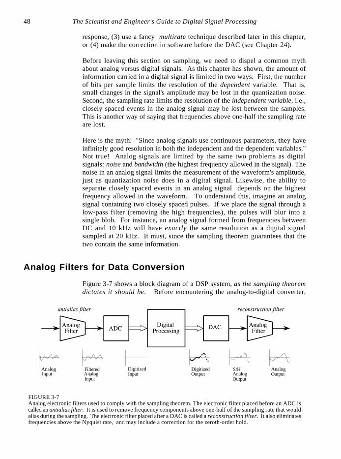
FIGURE 3-7Analog electronic filters used to comply with the sampling theorem. The electronic filter placed before an ADC iscalled an antialias filter. It is used to remove frequency components above one-half of the sampling rate that wouldalias during the sampling. The electronic filter placed after a DAC is called a reconstruction filter. It also eliminatesfrequencies above the Nyquist rate, and may include a correction for the zeroth-order hold.
response, (3) use a fancy multirate technique described later in this chapter,or (4) make the correction in software before the DAC (see Chapter 24).
Before leaving this section on sampling, we need to dispel a common mythabout analog versus digital signals. As this chapter has shown, the amount ofinformation carried in a digital signal is limited in two ways: First, the numberof bits per sample limits the resolution of the dependent variable. That is,small changes in the signal's amplitude may be lost in the quantization noise.Second, the sampling rate limits the resolution of the independent variable, i.e.,closely spaced events in the analog signal may be lost between the samples.This is another way of saying that frequencies above one-half the sampling rateare lost.
Here is the myth: "Since analog signals use continuous parameters, they haveinfinitely good resolution in both the independent and the dependent variables."Not true! Analog signals are limited by the same two problems as digitalsignals: noise and bandwidth (the highest frequency allowed in the signal). Thenoise in an analog signal limits the measurement of the waveform's amplitude,just as quantization noise does in a digital signal. Likewise, the ability toseparate closely spaced events in an analog signal depends on the highestfrequency allowed in the waveform. To understand this, imagine an analogsignal containing two closely spaced pulses. If we place the signal through alow-pass filter (removing the high frequencies), the pulses will blur into asingle blob. For instance, an analog signal formed from frequencies betweenDC and 10 kHz will have exactly the same resolution as a digital signalsampled at 20 kHz. It must, since the sampling theorem guarantees that thetwo contain the same information.
Analog Filters for Data Conversion
Figure 3-7 shows a block diagram of a DSP system, as the sampling theoremdictates it should be. Before encountering the analog-to-digital converter,

Chapter 3- ADC and DAC 49
the input signal is processed with an electronic low-pass filter to remove allfrequencies above the Nyquist frequency (one-half the sampling rate). This isdone to prevent aliasing during sampling, and is correspondingly called anantialias filter. On the other end, the digitized signal is passed through adigital-to-analog converter and another low-pass filter set to the Nyquistfrequency. This output filter is called a reconstruction filter, and may includethe previously described zeroth-order-hold frequency boost. Unfortunately,there is a serious problem with this simple model: the limitations of electronicfilters can be as bad as the problems they are trying to prevent.
If your main interest is in software, you are probably thinking that you don'tneed to read this section. Wrong! Even if you have vowed never to touch anoscilloscope, an understanding of the properties of analog filters is importantfor successful DSP. First, the characteristics of every digitized signal youencounter will depend on what type of antialias filter was used when it wasacquired. If you don't understand the nature of the antialias filter, you cannotunderstand the nature of the digital signal. Second, the future of DSP is toreplace hardware with software. For example, the multirate techniquespresented later in this chapter reduce the need for antialias and reconstructionfilters by fancy software tricks. If you don't understand the hardware, youcannot design software to replace it. Third, much of DSP is related to digitalfilter design. A common strategy is to start with an equivalent analog filter,and convert it into software. Later chapters assume you have a basicknowledge of analog filter techniques.
Three types of analog filters are commonly used: Chebyshev, Butterworth,and Bessel (also called a Thompson filter). Each of these is designed tooptimize a different performance parameter. The complexity of each filtercan be adjusted by selecting the number of poles and zeros, mathematicalterms that will be discussed in later chapters. The more poles in a filter,the more electronics it requires, and the better it performs. Each of thesenames describe what the filter does, not a particular arrangement ofresistors and capacitors. For example, a six pole Bessel filter can beimplemented by many different types of circuits, all of which have the sameoverall characteristics. For DSP purposes, the characteristics of thesefilters are more important than how they are constructed. Nevertheless, wewill start with a short segment on the electronic design of these filters toprovide an overall framework.
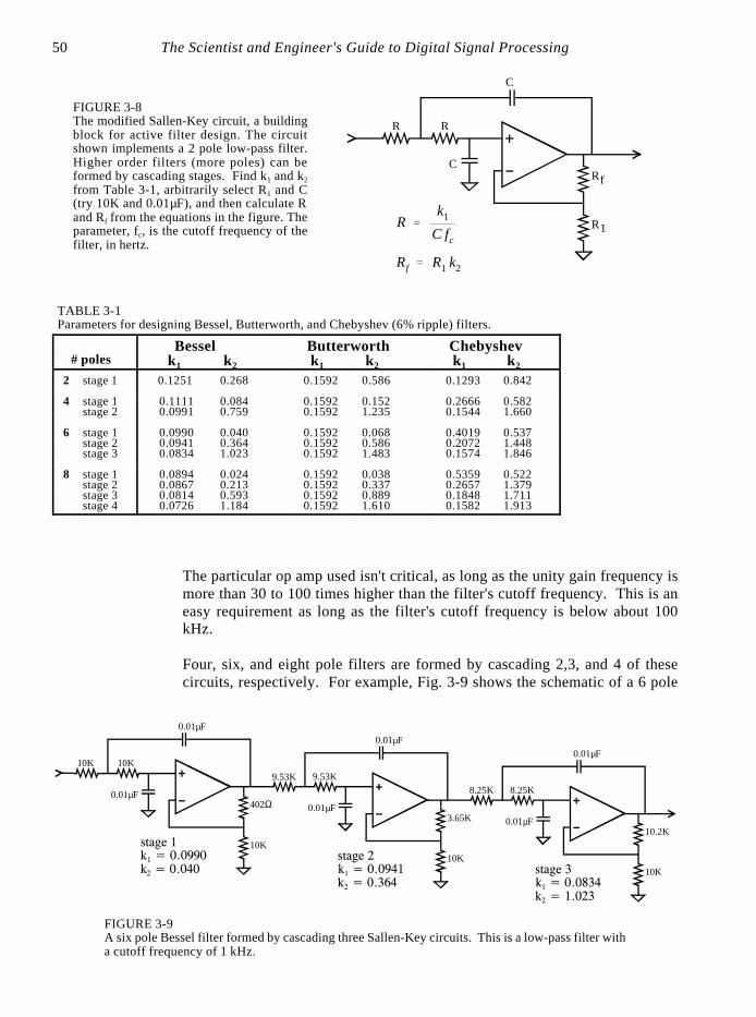
Figure 3-8 shows a common building block for analog filter design, themodified Sallen-Key circuit. This is named after the authors of a 1950s paperdescribing the technique. The circuit shown is a two pole low-pass filter thatcan be configured as any of the three basic types. Table 3-1 provides thenecessary information to select the appropriate resistors and capacitors. Forexample, to design a 1 kHz, 2 pole Butterworth filter, Table 3-1 provides theparameters: k1 = 0.1592 and k2 = 0.586. Arbitrarily selecting R1 = 10K andC = 0.01uF (common values for op amp circuits), R and Rf can be calculatedas 15.95K and 5.86K, respectively. Rounding these last two values to thenearest 1% standard resistors, results in R = 15.8K and Rf = 5.90K All of thecomponents should be 1% precision or better.
The Scientist and Engineer's Guide to Digital Signal Processing50
TABLE 3-1Parameters for designing Bessel, Butterworth, and Chebyshev (6% ripple) filters.
Bessel Butterworth Chebyshev # poles k1 k2 k1 k2 k1 k2
2 stage 1 0.1251 0.268 0.1592 0.586 0.1293 0.842
4 stage 1 0.1111 0.084 0.1592 0.152 0.2666 0.582stage 2 0.0991 0.759 0.1592 1.235 0.1544 1.660
6 stage 1 0.0990 0.040 0.1592 0.068 0.4019 0.537stage 2 0.0941 0.364 0.1592 0.586 0.2072 1.448stage 3 0.0834 1.023 0.1592 1.483 0.1574 1.846
8 stage 1 0.0894 0.024 0.1592 0.038 0.5359 0.522stage 2 0.0867 0.213 0.1592 0.337 0.2657 1.379stage 3 0.0814 0.593 0.1592 0.889 0.1848 1.711stage 4 0.0726 1.184 0.1592 1.610 0.1582 1.913
FIGURE 3-8The modified Sallen-Key circuit, a buildingblock for active filter design. The circuitshown implements a 2 pole low-pass filter.Higher order filters (more poles) can beformed by cascading stages. Find k1 and k2
from Table 3-1, arbitrarily select R1 and C(try 10K and 0.01µF), and then calculate Rand Rf from the equations in the figure. Theparameter, fc, is the cutoff frequency of thefilter, in hertz.
Rf
R1
C
C
R R
R 'k1
C fc
Rf ' R1 k2
402S
10K
0.01µF
0.01µF
10K 10K
3.65K
10K
0.01µF
0.01µF
9.53K 9.53K
10.2K
10K
0.01µF
0.01µF
8.25K 8.25K
k1 = 0.0990k2 = 0.040
stage 1
k1 = 0.0941k2 = 0.364
stage 2
k1 = 0.0834k2 = 1.023
stage 3
FIGURE 3-9A six pole Bessel filter formed by cascading three Sallen-Key circuits. This is a low-pass filter witha cutoff frequency of 1 kHz.
The particular op amp used isn't critical, as long as the unity gain frequency ismore than 30 to 100 times higher than the filter's cutoff frequency. This is aneasy requirement as long as the filter's cutoff frequency is below about 100kHz.
Four, six, and eight pole filters are formed by cascading 2,3, and 4 of thesecircuits, respectively. For example, Fig. 3-9 shows the schematic of a 6 pole

Chapter 3- ADC and DAC 51
time
low f
high f
time time
high R
low R
time
Resistor-Capacitor
Switched Capacitor
R
C
CC/100
f
FIGURE 3-10Switched capacitor filter operation. Switched capacitor filters use switches and capacitors to mimicresistors. As shown by the equivalent step responses, two capacitors and one switch can perform thesame function as a resistor-capacitor network.
volta
ge
volta
gevo
ltage
volta
ge
Bessel filter created by cascading three stages. Each stage has different valuesfor k1 and k2 as provided by Table 3-1, resulting in different resistors andcapacitors being used. Need a high-pass filter? Simply swap the R and Ccomponents in the circuits (leaving Rf and R1 alone).
This type of circuit is very common for small quantity manufacturing and R&Dapplications; however, serious production requires the filter to be made as anintegrated circuit. The problem is, it is difficult to make resistors directly insilicon. The answer is the switched capacitor filter. Figure 3-10 illustratesits operation by comparing it to a simple RC network. If a step function is fedinto an RC low-pass filter, the output rises exponentially until it matches theinput. The voltage on the capacitor doesn't change instantaneously, because theresistor restricts the flow of electrical charge. The switched capacitor filter operates by replacing the basic resistor-capacitor network with two capacitors and an electronic switch. The newlyadded capacitor is much smaller in value than the already existingcapacitor, say, 1% of its value. The switch alternately connects the smallcapacitor between the input and the output at a very high frequency,typically 100 times faster than the cutoff frequency of the filter. When theswitch is connected to the input, the small capacitor rapidly charges towhatever voltage is presently on the input. When the switch is connectedto the output, the charge on the small capacitor is transferred to the largecapacitor. In a resistor, the rate of charge transfer is determined by itsresistance. In a switched capacitor circuit, the rate of charge transfer isdetermined by the value of the small capacitor and by the switchingfrequency. This results in a very useful feature of switched capacitor

The Scientist and Engineer's Guide to Digital Signal Processing52
filters: the cutoff frequency of the filter is directly proportional to the clockfrequency used to drive the switches. This makes the switched capacitor filterideal for data acquisition systems that operate with more than one samplingrate. These are easy-to-use devices; pay ten bucks and have the performanceof an eight pole filter inside a single 8 pin IC.
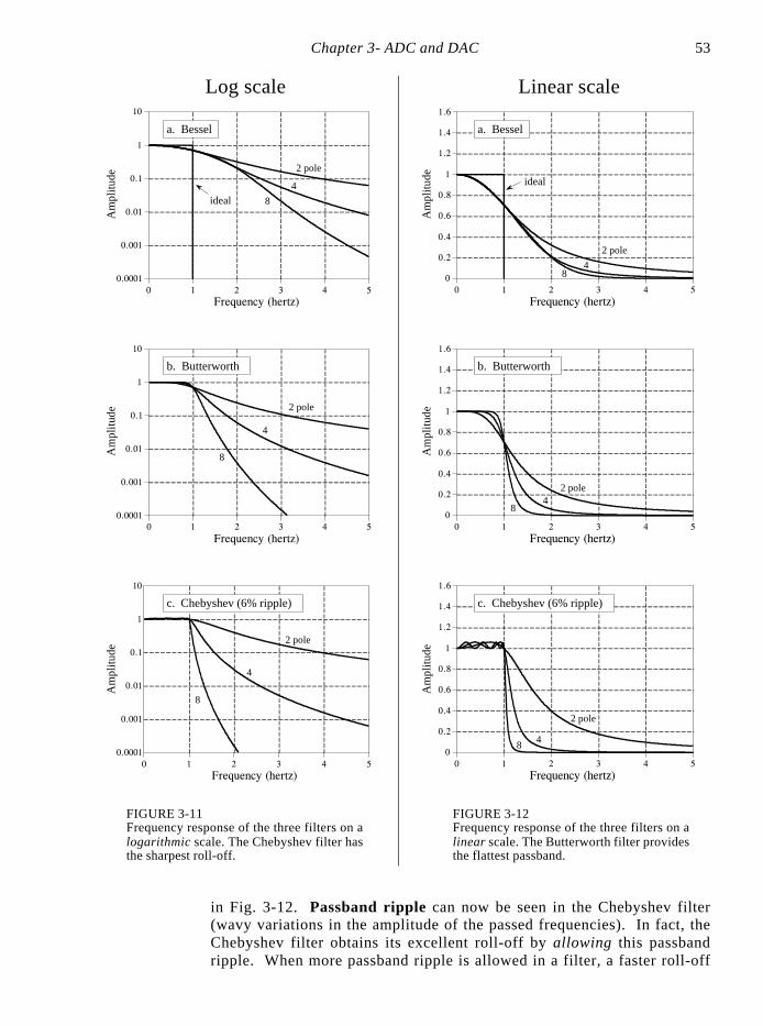
Now for the important part: the characteristics of the three classic filter types.The first performance parameter we want to explore is cutoff frequencysharpness. A low-pass filter is designed to block all frequencies above thecutoff frequency (the stopband), while passing all frequencies below (thepassband). Figure 3-11 shows the frequency response of these three filters ona logarithmic (dB) scale. These graphs are shown for filters with a one hertzcutoff frequency, but they can be directly scaled to whatever cutoff frequencyyou need to use. How do these filters rate? The Chebyshev is clearly the best,the Butterworth is worse, and the Bessel is absolutely ghastly! As youprobably surmised, this is what the Chebyshev is designed to do, roll-off (dropin amplitude) as rapidly as possible.
Unfortunately, even an 8 pole Chebyshev isn't as good as you would like foran antialias filter. For example, imagine a 12 bit system sampling at 10,000samples per second. The sampling theorem dictates that any frequency above5 kHz will be aliased, something you want to avoid. With a little guess work,you decide that all frequencies above 5 kHz must be reduced in amplitude bya factor of 100, insuring that any aliased frequencies will have an amplitude ofless than one percent. Looking at Fig. 3-11c, you find that an 8 poleChebyshev filter, with a cutoff frequency of 1 hertz, doesn't reach anattenuation (signal reduction) of 100 until about 1.35 hertz. Scaling this to theexample, the filter's cutoff frequency must be set to 3.7 kHz so that everythingabove 5 kHz will have the required attenuation. This results in the frequencyband between 3.7 kHz and 5 kHz being wasted on the inadequate roll-off of theanalog filter.
A subtle point: the attenuation factor of 100 in this example is probablysufficient even though there are 4096 steps in 12 bits. From Fig. 3-4, 5100hertz will alias to 4900 hertz, 6000 hertz will alias to 4000 hertz, etc. Youdon't care what the amplitudes of the signals between 5000 and 6300 hertz are,because they alias into the unusable region between 3700 hertz and 5000 hertz.In order for a frequency to alias into the filter's passband (0 to 3.7 kHz), itmust be greater than 6300 hertz, or 1.7 times the filter's cutoff frequency of3700 hertz. As shown in Fig. 3-11c, the attenuation provided by an 8 poleChebyshev filter at 1.7 times the cutoff frequency is about 1300, much moreadequate than the 100 we started the analysis with. The moral to this story: Inmost systems, the frequency band between about 0.4 and 0.5 of the samplingfrequency is an unusable wasteland of filter roll-off and aliased signals. Thisis a direct result of the limitations of analog filters.
The frequency response of the perfect low-pass filter is flat across the entirepassband. All of the filters look great in this respect in Fig. 3-11, but onlybecause the vertical axis is displayed on a logarithmic scale. Another story istold when the graphs are converted to a linear vertical scale, as is shown
Chapter 3- ADC and DAC 53
Frequency (hertz)0 1 2 3 4 5
0.0001
0.001
0.01
0.1
1
10
8
4
2 pole
a. Bessel
ideal
Frequency (hertz)0 1 2 3 4 5
0
0.2
0.4
0.6
0.8
1
1.2
1.4
1.6
84
2 pole
a. Bessel
ideal
Frequency (hertz)0 1 2 3 4 5
0.0001
0.001
0.01
0.1
1
10
8
4
2 pole
b. Butterworth
Frequency (hertz)0 1 2 3 4 5
0
0.2
0.4
0.6
0.8
1
1.2
1.4
1.6
84
2 pole
b. Butterworth
Frequency (hertz)0 1 2 3 4 5
0.0001
0.001
0.01
0.1
1
10
8
4
2 pole
c. Chebyshev (6% ripple)
Frequency (hertz)0 1 2 3 4 5
0
0.2
0.4
0.6
0.8
1
1.2
1.4
1.6
4
2 pole
8
c. Chebyshev (6% ripple)
Linear scale
Am
plitu
deA
mpl
itude
Am
plitu
deA
mpl
itude
Am
plitu
de
Log scaleA
mpl
itude
FIGURE 3-12Frequency response of the three filters on alinear scale. The Butterworth filter providesthe flattest passband.
FIGURE 3-11Frequency response of the three filters on alogarithmic scale. The Chebyshev filter hasthe sharpest roll-off.
in Fig. 3-12. Passband ripple can now be seen in the Chebyshev filter(wavy variations in the amplitude of the passed frequencies). In fact, theChebyshev filter obtains its excellent roll-off by allowing this passbandripple. When more passband ripple is allowed in a filter, a faster roll-off
The Scientist and Engineer's Guide to Digital Signal Processing54
Time (seconds)0 1 2 3 4
0.0
0.2
0.4
0.6
0.8
1.0
1.2
1.4
1.6
8 pole
4
2
a. Bessel
Time (seconds)0 1 2 3 4
0.0
0.2
0.4
0.6
0.8
1.0
1.2
1.4
1.6
8 pole
2
b. Butterworth
4
FIGURE 3-13Step response of the three filters. The timesshown on the horizontal axis correspond to aone hertz cutoff frequency. The Bessel is theoptimum filter when overshoot and ringingmust be minimized.
Time (seconds)0 1 2 3 4
0.0
0.2
0.4
0.6
0.8
1.0
1.2
1.4
1.6
8 pole
4
2
c. Chebyshev (6% ripple)
Am
plitu
deA
mpl
itude
Am
plitu
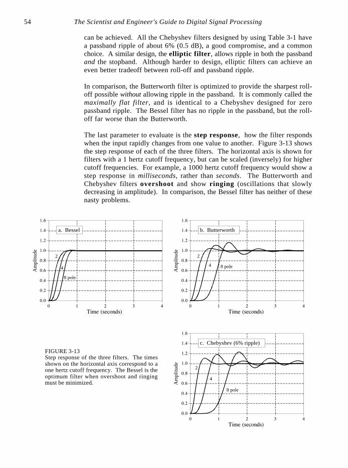
decan be achieved. All the Chebyshev filters designed by using Table 3-1 havea passband ripple of about 6% (0.5 dB), a good compromise, and a commonchoice. A similar design, the elliptic filter, allows ripple in both the passbandand the stopband. Although harder to design, elliptic filters can achieve aneven better tradeoff between roll-off and passband ripple.
In comparison, the Butterworth filter is optimized to provide the sharpest roll-off possible without allowing ripple in the passband. It is commonly called themaximally flat filter, and is identical to a Chebyshev designed for zeropassband ripple. The Bessel filter has no ripple in the passband, but the roll-off far worse than the Butterworth.
The last parameter to evaluate is the step response, how the filter respondswhen the input rapidly changes from one value to another. Figure 3-13 showsthe step response of each of the three filters. The horizontal axis is shown forfilters with a 1 hertz cutoff frequency, but can be scaled (inversely) for highercutoff frequencies. For example, a 1000 hertz cutoff frequency would show astep response in milliseconds, rather than seconds. The Butterworth andChebyshev filters overshoot and show ringing (oscillations that slowlydecreasing in amplitude). In comparison, the Bessel filter has neither of thesenasty problems.
Chapter 3- ADC and DAC 55
Time0 100 200 300 400 500
-0.5
0.0
0.5
1.0
1.5
a. Pulse waveform
Time0 100 200 300 400 500
-0.5
0.0
0.5
1.0
1.5
b. After Bessel filter
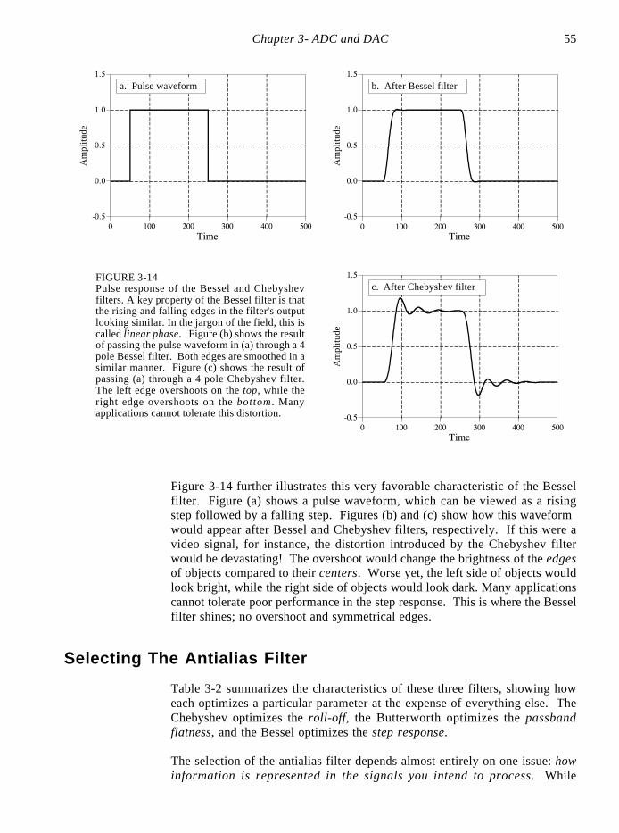
FIGURE 3-14Pulse response of the Bessel and Chebyshevfilters. A key property of the Bessel filter is thatthe rising and falling edges in the filter's outputlooking similar. In the jargon of the field, this iscalled linear phase. Figure (b) shows the resultof passing the pulse waveform in (a) through a 4pole Bessel filter. Both edges are smoothed in asimilar manner. Figure (c) shows the result ofpassing (a) through a 4 pole Chebyshev filter.The left edge overshoots on the top, while theright edge overshoots on the bottom . Manyapplications cannot tolerate this distortion.
Time0 100 200 300 400 500
-0.5
0.0
0.5
1.0
1.5
c. After Chebyshev filter
Am
plitu
deA
mpl
itude
Am
plitu
de
Figure 3-14 further illustrates this very favorable characteristic of the Besselfilter. Figure (a) shows a pulse waveform, which can be viewed as a risingstep followed by a falling step. Figures (b) and (c) show how this waveformwould appear after Bessel and Chebyshev filters, respectively. If this were avideo signal, for instance, the distortion introduced by the Chebyshev filterwould be devastating! The overshoot would change the brightness of the edgesof objects compared to their centers. Worse yet, the left side of objects wouldlook bright, while the right side of objects would look dark. Many applicationscannot tolerate poor performance in the step response. This is where the Besselfilter shines; no overshoot and symmetrical edges.
Selecting The Antialias Filter
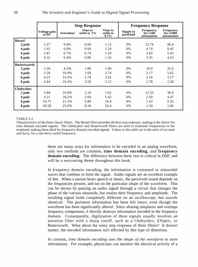
Table 3-2 summarizes the characteristics of these three filters, showing howeach optimizes a particular parameter at the expense of everything else. TheChebyshev optimizes the roll-off, the Butterworth optimizes the passbandflatness, and the Bessel optimizes the step response.
The selection of the antialias filter depends almost entirely on one issue: howinformation is represented in the signals you intend to process. While
The Scientist and Engineer's Guide to Digital Signal Processing56
TABLE 3-2Characteristics of the three classic filters. The Bessel filter provides the best step response, making it the choice fortime domain encoded signals. The Chebyshev and Butterworth filters are used to eliminate frequencies in thestopband, making them ideal for frequency domain encoded signals. Values in this table are in the units of secondsand hertz, for a one hertz cutoff frequency.
Step Response Frequency ResponseVoltage gain
at DC OvershootTime to
settle to 1%Time tosettle to
0.1%Ripple inpassband
Frequencyfor x100
attenuation
Frequencyfor x1000
attenuation
Bessel2 pole 1.27 0.4% 0.60 1.12 0% 12.74 40.44 pole 1.91 0.9% 0.66 1.20 0% 4.74 8.456 pole 2.87 0.7% 0.74 1.18 0% 3.65 5.438 pole 4.32 0.4% 0.80 1.16 0% 3.35 4.53
Butterworth2 pole 1.59 4.3% 1.06 1.66 0% 10.0 31.64 pole 2.58 10.9% 1.68 2.74 0% 3.17 5.626 pole 4.21 14.3% 2.74 3.92 0% 2.16 3.178 pole 6.84 16.4% 3.50 5.12 0% 1.78 2.38
Chebyshev2 pole 1.84 10.8% 1.10 1.62 6% 12.33 38.94 pole 4.21 18.2% 3.04 5.42 6% 2.59 4.476 pole 10.71 21.3% 5.86 10.4 6% 1.63 2.268 pole 28.58 23.0% 8.34 16.4 6% 1.34 1.66
there are many ways for information to be encoded in an analog waveform,only two methods are common, time domain encoding, and frequencydomain encoding. The difference between these two is critical in DSP, andwill be a reoccurring theme throughout this book.
In frequency domain encoding, the information is contained in sinusoidalwaves that combine to form the signal. Audio signals are an excellent exampleof this. When a person hears speech or music, the perceived sound depends onthe frequencies present, and not on the particular shape of the waveform. Thiscan be shown by passing an audio signal through a circuit that changes thephase of the various sinusoids, but retains their frequency and amplitude. Theresulting signal looks completely different on an oscilloscope, but soundsidentical. The pertinent information has been left intact, even though thewaveform has been significantly altered. Since aliasing misplaces and overlapsfrequency components, it directly destroys information encoded in the frequencydomain. Consequently, digitization of these signals usually involves anantialias filter with a sharp cutoff, such as a Chebyshev, Elliptic, orButterworth. What about the nasty step response of these filters? It doesn'tmatter; the encoded information isn't affected by this type of distortion.
In contrast, time domain encoding uses the shape of the waveform to storeinformation. For example, physicians can monitor the electrical activity of a
Chapter 3- ADC and DAC 57
person's heart by attaching electrodes to their chest and arms (anelectrocardiogram or EKG). The shape of the EKG waveform provides theinformation being sought, such as when the various chambers contract duringa heartbeat. Images are another example of this type of signal. Rather than awaveform that varies over time, images encode information in the shape of awaveform that varies over distance. Pictures are formed from regions ofbrightness and color, and how they relate to other regions of brightness andcolor. You don't look at the Mona Lisa and say, "My, what an interestingcollection of sinusoids."
Here's the problem: The sampling theorem is an analysis of what happens inthe frequency domain during digitization. This makes it ideal to under-standthe analog-to-digital conversion of signals having their information encoded inthe frequency domain. However, the sampling theorem is little help inunderstanding how time domain encoded signals should be digitized. Let's takea closer look.
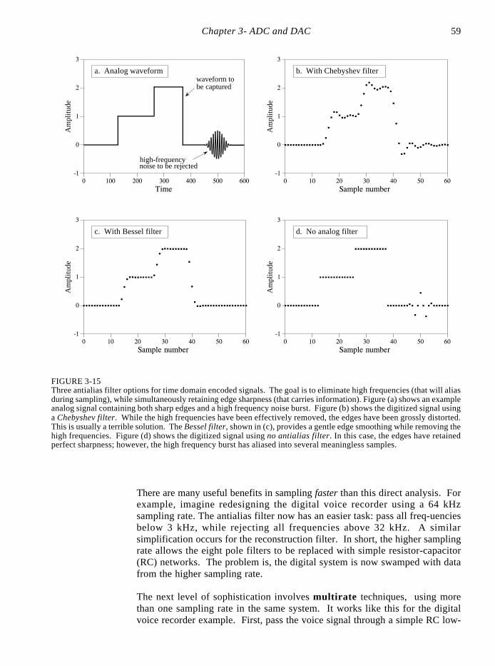
Figure 3-15 illustrates the choices for digitizing a time domain encoded signal.Figure (a) is an example analog signal to be digitized. In this case, theinformation we want to capture is the shape of the rectangular pulses. A shortburst of a high frequency sine wave is also included in this example signal.This represents wideband noise, interference, and similar junk that alwaysappears on analog signals. The other figures show how the digitized signalwould appear with different antialias filter options: a Chebyshev filter, a Besselfilter, and no filter.
It is important to understand that none of these options will allow the originalsignal to be reconstructed from the sampled data. This is because the originalsignal inherently contains frequency components greater than one-half of thesampling rate. Since these frequencies cannot exist in the digitized signal, thereconstructed signal cannot contain them either. These high frequencies resultfrom two sources: (1) noise and interference, which you would like toeliminate, and (2) sharp edges in the waveform, which probably containinformation you want to retain.
The Chebyshev filter, shown in (b), attacks the problem by aggressivelyremoving all high frequency components. This results in a filtered analogsignal that can be sampled and later perfectly reconstructed. However, thereconstructed analog signal is identical to the filtered signal, not the originalsignal. Although nothing is lost in sampling, the waveform has been severelydistorted by the antialias filter. As shown in (b), the cure is worse than thedisease! Don't do it!
The Bessel filter, (c), is designed for just this problem. Its output closelyresembles the original waveform, with only a gentle rounding of the edges.By adjusting the filter's cutoff frequency, the smoothness of the edges canbe traded for elimination of high frequency components in the signal.Using more poles in the filter allows a better tradeoff between these twoparameters. A common guideline is to set the cutoff frequency at aboutone-quarter of the sampling frequency. This results in about two samples
The Scientist and Engineer's Guide to Digital Signal Processing58
along the rising portion of each edge. Notice that both the Bessel and theChebyshev filter have removed the burst of high frequency noise present inthe original signal.
The last choice is to use no antialias filter at all, as is shown in (d). Thishas the strong advantage that the value of each sample is identical to thevalue of the original analog signal. In other words, it has perfect edgesharpness; a change in the original signal is immediately mirrored in thedigital data. The disadvantage is that aliasing can distort the signal. Thistakes two different forms. First, high frequency interference and noise,such as the example sinusoidal burst, will turn into meaningless samples,as shown in (d). That is, any high frequency noise present in the analogsignal will appear as aliased noise in the digital signal. In a more generalsense, this is not a problem of the sampling, but a problem of the upstreamanalog electronics. It is not the ADC's purpose to reduce noise andinterference; this is the responsibility of the analog electronics before thedigitization takes place. It may turn out that a Bessel filter should beplaced before the digitizer to control this problem. However, this means thefilter should be viewed as part of the analog processing, not something thatis being done for the sake of the digitizer.
The second manifestation of aliasing is more subtle. When an event occursin the analog signal (such as an edge), the digital signal in (d) detects thechange on the next sample. There is no information in the digital data toindicate what happens between samples. Now, compare using no filter withusing a Bessel filter for this problem. For example, imagine drawingstraight lines between the samples in (c). The time when this constructedline crosses one-half the amplitude of the step provides a subsampleestimate of when the edge occurred in the analog signal. When no filter isused, this subsample information is completely lost. You don't need a fancytheorem to evaluate how this will affect your particular situation, just agood understanding of what you plan to do with the data once is it acquired.
Multirate Data Conversion
There is a strong trend in electronics to replace analog circuitry withdigital algorithms. Data conversion is an excellent example of this.Consider the design of a digital voice recorder, a system that will digitizea voice signal, store the data in digital form, and later reconstruct thesignal for playback. To recreate intelligible speech, the system mustcapture the frequencies between about 100 and 3000 hertz. However, theanalog signal produced by the microphone also contains much higherfrequencies, say to 40 kHz. The brute force approach is to pass the analogsignal through an eight pole low-pass Chebyshev filter at 3 kHz, and thensample at 8 kHz. On the other end, the DAC reconstructs the analog signalat 8 kHz with a zeroth order hold. Another Chebyshev filter at 3 kHz isused to produce the final voice signal.
Chapter 3- ADC and DAC 59
Sample number0 10 20 30 40 50 60
-1
0
1
2
3
d. No analog filter
Time0 100 200 300 400 500 600
-1
0
1
2
3
a. Analog waveformwaveform tobe captured
high-frequencynoise to be rejected
Sample number0 10 20 30 40 50 60
-1
0
1
2
3
b. With Chebyshev filter
FIGURE 3-15Three antialias filter options for time domain encoded signals. The goal is to eliminate high frequencies (that will aliasduring sampling), while simultaneously retaining edge sharpness (that carries information). Figure (a) shows an exampleanalog signal containing both sharp edges and a high frequency noise burst. Figure (b) shows the digitized signal usinga Chebyshev filter. While the high frequencies have been effectively removed, the edges have been grossly distorted.This is usually a terrible solution. The Bessel filter, shown in (c), provides a gentle edge smoothing while removing thehigh frequencies. Figure (d) shows the digitized signal using no antialias filter. In this case, the edges have retainedperfect sharpness; however, the high frequency burst has aliased into several meaningless samples.
Sample number0 10 20 30 40 50 60
-1
0
1
2
3
c. With Bessel filter
Am
plitu
deA
mpl
itude
Am
plitu
deA
mpl
itude
There are many useful benefits in sampling faster than this direct analysis. Forexample, imagine redesigning the digital voice recorder using a 64 kHzsampling rate. The antialias filter now has an easier task: pass all freq-uenciesbelow 3 kHz, while rejecting all frequencies above 32 kHz. A similarsimplification occurs for the reconstruction filter. In short, the higher samplingrate allows the eight pole filters to be replaced with simple resistor-capacitor(RC) networks. The problem is, the digital system is now swamped with datafrom the higher sampling rate.
The next level of sophistication involves multirate techniques, using morethan one sampling rate in the same system. It works like this for the digitalvoice recorder example. First, pass the voice signal through a simple RC low-
The Scientist and Engineer's Guide to Digital Signal Processing60
pass filter and sample the data at 64 kHz. The resulting digital data containsthe desired voice band between 100 and 3000 hertz, but also has an unusableband between 3 kHz and 32 kHz. Second, remove these unusable frequenciesin software, by using a digital low-pass filter at 3 kHz. Third, resample thedigital signal from 64 kHz to 8 kHz by simply discarding every seven out ofeight samples, a procedure called decimation. The resulting digital data isequivalent to that produced by aggressive analog filtering and direct 8 kHzsampling.
Multirate techniques can also be used in the output portion of our examplesystem. The 8 kHz data is pulled from memory and converted to a 64 kHzsampling rate, a procedure called interpolation. This involves placing sevensamples, with a value of zero, between each of the samples obtained frommemory. The resulting signal is a digital impulse train, containing the desiredvoice band between 100 and 3000 hertz, plus spectral duplications between 3kHz and 32 kHz. Refer back to Figs. 3-6 a&b to understand why this it true.Everything above 3 kHz is then removed with a digital low-pass filter. Afterconversion to an analog signal through a DAC, a simple RC network is all thatis required to produce the final voice signal.
Multirate data conversion is valuable for two reasons: (1) it replacesanalog components with software, a clear economic advantage in mass-produced products, and (2) it can achieve higher levels of performance incritical applications. For example, compact disc audio systems usetechniques of this type to achieve the best possible sound quality. Thisincreased performance is a result of replacing analog components (1%precision), with digital algorithms (0.0001% precision from round-offerror). As discussed in upcoming chapters, digital filters outperform analogfilters by hundreds of times in key areas.
Single Bit Data Conversion
A popular technique in telecommunications and high fidelity music reproductionis single bit ADC and DAC. These are multirate techniques where a highersampling rate is traded for a lower number of bits. In the extreme, only asingle bit is needed for each sample. While there are many different circuitconfigurations, most are based on the use of delta modulation. Threeexample circuits will be presented to give you a flavor of the field. All ofthese circuits are implemented in IC's, so don't worry where all of theindividual transistors and op amps should go. No one is going to ask you tobuild one of these circuits from basic components.
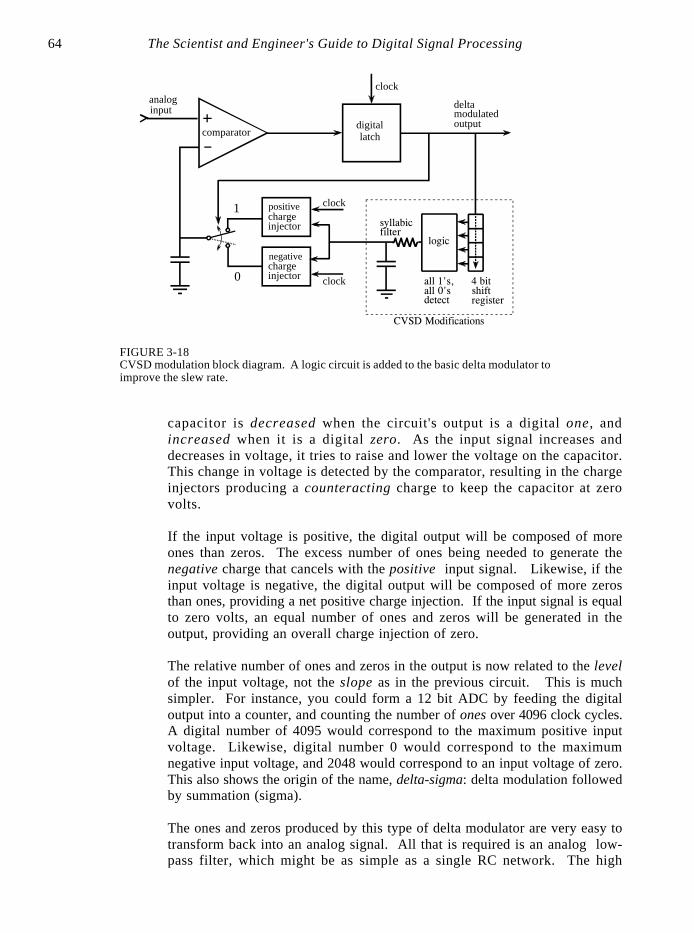
Figure 3-16 shows the block diagram of a typical delta modulator. Theanalog input is a voice signal with an amplitude of a few volts, while theoutput signal is a stream of digital ones and zeros. A comparator decideswhich has the greater voltage, the incoming analog signal, or the voltagestored on the capacitor. This decision, in the form of a digital one or zero,is applied to the input of the latch. At each clock pulse, typically at a fewhundred kilohertz, the latch transfers whatever digital state appears on its
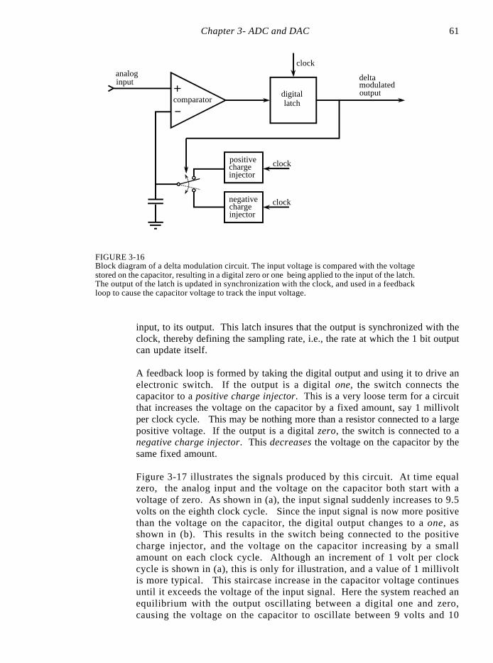
Chapter 3- ADC and DAC 61
digitallatchcomparator
chargeinjector
negative
chargeinjector
positive
clockanaloginput delta
modulatedoutput
clock
clock
FIGURE 3-16Block diagram of a delta modulation circuit. The input voltage is compared with the voltagestored on the capacitor, resulting in a digital zero or one being applied to the input of the latch.The output of the latch is updated in synchronization with the clock, and used in a feedbackloop to cause the capacitor voltage to track the input voltage.
input, to its output. This latch insures that the output is synchronized with theclock, thereby defining the sampling rate, i.e., the rate at which the 1 bit outputcan update itself.
A feedback loop is formed by taking the digital output and using it to drive anelectronic switch. If the output is a digital one, the switch connects thecapacitor to a positive charge injector. This is a very loose term for a circuitthat increases the voltage on the capacitor by a fixed amount, say 1 millivoltper clock cycle. This may be nothing more than a resistor connected to a largepositive voltage. If the output is a digital zero, the switch is connected to anegative charge injector. This decreases the voltage on the capacitor by thesame fixed amount.
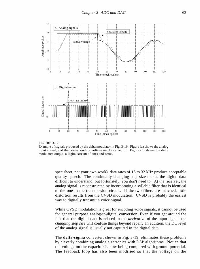
Figure 3-17 illustrates the signals produced by this circuit. At time equalzero, the analog input and the voltage on the capacitor both start with avoltage of zero. As shown in (a), the input signal suddenly increases to 9.5volts on the eighth clock cycle. Since the input signal is now more positivethan the voltage on the capacitor, the digital output changes to a one, asshown in (b). This results in the switch being connected to the positivecharge injector, and the voltage on the capacitor increasing by a smallamount on each clock cycle. Although an increment of 1 volt per clockcycle is shown in (a), this is only for illustration, and a value of 1 millivoltis more typical. This staircase increase in the capacitor voltage continuesuntil it exceeds the voltage of the input signal. Here the system reached anequilibrium with the output oscillating between a digital one and zero,causing the voltage on the capacitor to oscillate between 9 volts and 10
The Scientist and Engineer's Guide to Digital Signal Processing62
volts. In this manner, the feedback of the circuit forces the capacitorvoltage to track the voltage of the input signal. If the input signal changesvery rapidly, the voltage on the capacitor changes at a constant rate until amatch is obtained. This constant rate of change is called the slew rate, justas in other electronic devices such as op amps.
Now, consider the characteristics of the delta modulated output signal. If theanalog input is increasing in value, the output signal will consist of more onesthan zeros. Likewise, if the analog input is decreasing in value, the output willconsist of more zeros than ones. If the analog input is constant, the digitaloutput will alternate between zero and one with an equal number of each. Putin more general terms, the relative number of ones versus zeros is directlyproportional to the slope (derivative) of the analog input.
This circuit is a cheap method of transforming an analog signal into a serialstream of ones and zeros for transmission or digital storage. An especiallyattractive feature is that all the bits have the same meaning, unlike theconventional serial format: start bit, LSB, ,MSB, stop bit. The circuit at@ @ @the receiver is identical to the feedback portion of the transmitting circuit. Justas the voltage on the capacitor in the transmitting circuit follows the analoginput, so does the voltage on the capacitor in the receiving circuit. That is, thecapacitor voltage shown in (a) also represents how the reconstructed signalwould appear.
A critical limitation of this circuit is the unavoidable tradeoff between (1)maximum slew rate, (2) quantization size, and (3) data rate. In particular, ifthe maximum slew rate and quantization size are adjusted to acceptable valuesfor voice communication, the data rate ends up in the MHz range. This is toohigh to be of commercial value. For instance, conventional sampling of a voicesignal requires only about 64,000 bits per second.
A solution to this problem is shown in Fig. 3-18, the Continuously VariableSlope Delta (CVSD) modulator, a technique implemented in the MotorolaMC3518 family. In this approach, the clock rate and the quantization size areset to something acceptable, say 30 kHz, and 2000 levels. This results in aterrible slew rate, which you correct with additional circuitry. In operation, ashift resister continually looks at the last four bits that the system has produced.If the circuit is in a slew rate limited condition, the last four bits will be allones (positive slope) or all zeros (negative slope). A logic circuit detects thissituation and produces an analog signal that increase the level of chargeproduced by the charge injectors. This boosts the slew rate by increasing thesize of the voltage steps being applied to the capacitor.
An analog filter is usually placed between the logic circuitry and the chargeinjectors. This allows the step size to depend on how long the circuit hasbeen in a slew limited condition. As long as the circuit is slew limited, thestep size keeps getting larger and larger. This is often called a syllabicfilter, since its characteristics depend on the average length of the syllablesmaking up speech. With proper optimization (from the chip manufacturer's
Chapter 3- ADC and DAC 63
Time (clock cycles)0 10 20 30 40 50 60 70 80 90 100 110 120
-10
-5
0
5
10
15
a. Analog signals
signal voltage
capacitor voltage
Time (clock cycles)0 10 20 30 40 50 60 70 80 90 100 110 120
-1
0
1
2
3
slew rate limited
b. Digital output
FIGURE 3-17Example of signals produced by the delta modulator in Fig. 3-16. Figure (a) shows the analoginput signal, and the corresponding voltage on the capacitor. Figure (b) shows the deltamodulated output, a digital stream of ones and zeros.
Dig
ital l
ogic
sta
teA
mpl
itude
(vo
lts)
spec sheet, not your own work), data rates of 16 to 32 kHz produce acceptablequality speech. The continually changing step size makes the digital datadifficult to understand, but fortunately, you don't need to. At the receiver, theanalog signal is reconstructed by incorporating a syllabic filter that is identicalto the one in the transmission circuit. If the two filters are matched, littledistortion results from the CVSD modulation. CVSD is probably the easiestway to digitally transmit a voice signal.
While CVSD modulation is great for encoding voice signals, it cannot be usedfor general purpose analog-to-digital conversion. Even if you get around thefact that the digital data is related to the derivative of the input signal, thechanging step size will confuse things beyond repair. In addition, the DC levelof the analog signal is usually not captured in the digital data.
The delta-sigma converter, shown in Fig. 3-19, eliminates these problemsby cleverly combining analog electronics with DSP algorithms. Notice thatthe voltage on the capacitor is now being compared with ground potential.The feedback loop has also been modified so that the voltage on the
The Scientist and Engineer's Guide to Digital Signal Processing64
digitallatchcomparator
chargeinjector
negative
chargeinjector
positive
clockanaloginput delta
modulatedoutput
4 bitshiftregister
all 1's,all 0'sdetect
syllabicfilter
CVSD Modifications
1
0
clock
clock
logic
FIGURE 3-18CVSD modulation block diagram. A logic circuit is added to the basic delta modulator toimprove the slew rate.
capacitor is decreased when the circuit's output is a digital one, andincreased when it is a digital zero. As the input signal increases anddecreases in voltage, it tries to raise and lower the voltage on the capacitor.This change in voltage is detected by the comparator, resulting in the chargeinjectors producing a counteracting charge to keep the capacitor at zerovolts. If the input voltage is positive, the digital output will be composed of moreones than zeros. The excess number of ones being needed to generate thenegative charge that cancels with the positive input signal. Likewise, if theinput voltage is negative, the digital output will be composed of more zerosthan ones, providing a net positive charge injection. If the input signal is equalto zero volts, an equal number of ones and zeros will be generated in theoutput, providing an overall charge injection of zero.
The relative number of ones and zeros in the output is now related to the levelof the input voltage, not the slope as in the previous circuit. This is muchsimpler. For instance, you could form a 12 bit ADC by feeding the digitaloutput into a counter, and counting the number of ones over 4096 clock cycles.A digital number of 4095 would correspond to the maximum positive inputvoltage. Likewise, digital number 0 would correspond to the maximumnegative input voltage, and 2048 would correspond to an input voltage of zero.This also shows the origin of the name, delta-sigma: delta modulation followedby summation (sigma).
The ones and zeros produced by this type of delta modulator are very easy totransform back into an analog signal. All that is required is an analog low-pass filter, which might be as simple as a single RC network. The high
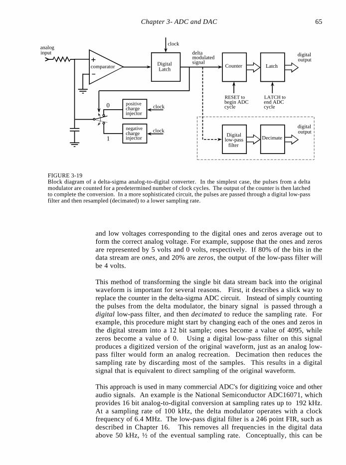
Chapter 3- ADC and DAC 65
DigitalLatchcomparator
chargeinjector
negative
chargeinjector
positive
clockanaloginput delta
modulatedsignal
0
1
Counter Latch
digitaloutput
begin ADCRESET to
end ADCcycle
LATCH to
cycle
Digital
digitaloutput
low-passfilter
Decimate
clock
clock
FIGURE 3-19Block diagram of a delta-sigma analog-to-digital converter. In the simplest case, the pulses from a deltamodulator are counted for a predetermined number of clock cycles. The output of the counter is then latchedto complete the conversion. In a more sophisticated circuit, the pulses are passed through a digital low-passfilter and then resampled (decimated) to a lower sampling rate.
and low voltages corresponding to the digital ones and zeros average out toform the correct analog voltage. For example, suppose that the ones and zerosare represented by 5 volts and 0 volts, respectively. If 80% of the bits in thedata stream are ones, and 20% are zeros, the output of the low-pass filter willbe 4 volts.
This method of transforming the single bit data stream back into the originalwaveform is important for several reasons. First, it describes a slick way toreplace the counter in the delta-sigma ADC circuit. Instead of simply countingthe pulses from the delta modulator, the binary signal is passed through adigital low-pass filter, and then decimated to reduce the sampling rate. Forexample, this procedure might start by changing each of the ones and zeros inthe digital stream into a 12 bit sample; ones become a value of 4095, whilezeros become a value of 0. Using a digital low-pass filter on this signalproduces a digitized version of the original waveform, just as an analog low-pass filter would form an analog recreation. Decimation then reduces thesampling rate by discarding most of the samples. This results in a digitalsignal that is equivalent to direct sampling of the original waveform.
This approach is used in many commercial ADC's for digitizing voice and otheraudio signals. An example is the National Semiconductor ADC16071, whichprovides 16 bit analog-to-digital conversion at sampling rates up to 192 kHz.At a sampling rate of 100 kHz, the delta modulator operates with a clockfrequency of 6.4 MHz. The low-pass digital filter is a 246 point FIR, such asdescribed in Chapter 16. This removes all frequencies in the digital dataabove 50 kHz, ½ of the eventual sampling rate. Conceptually, this can be
The Scientist and Engineer's Guide to Digital Signal Processing66
viewed as forming a digital signal at 6.4 MHz, with each sample representedby 16 bits. The signal is then decimated from 6.4 MHz to 100 kHz,accomplished by deleting every 63 out of 64 samples. In actual operation,much more goes on inside of this device than described by this simplediscussion.
Delta-sigma converters can also be used for digital-to-analog conversion ofvoice and audio signals. The digital signal is retrieved from memory, andconverted into a delta modulated stream of ones and zeros. As mentionedabove, this single bit signal can easily be changed into the reconstructed analogsignal with a simple low-pass analog filter. As with the antialias filter, usuallyonly a single RC network is required. This is because the majority of thefiltration is handled by the high-performance digital filters.
Delta-sigma ADC's have several quirks that limit their use to specificapplications. For example, it is difficult to multiplex their inputs. When theinput is switched from one signal to another, proper operation is not establisheduntil the digital filter can clear itself of data from the previous signal. Delta-sigma converters are also limited in another respect: you don't know exactlywhen each sample was taken. Each acquired sample is a composite of the onebit information taken over a segment of the input signal. This is not a problemfor signals encoded in the frequency domain, such as audio, but it is asignificant limitation for time domain encoded signals. To understand the shapeof a signal's waveform, you often need to know the precise instant each samplewas taken. Lastly, most of these devices are specifically designed for audioapplications, and their performance specifications are quoted accordingly. Forexample, a 16 bit ADC used for voice signals does not necessarily mean thateach sample has 16 bits of precision. Much more likely, the manufacturer isstating that voice signals can be digitized to 16 bits of dynamic range. Don'texpect to get a full 16 bits of useful information from this device for generalpurpose data acquisition.
While these explanations and examples provide an introduction to single bitADC and DAC, it must be emphasized that they are simplified descriptions ofsophisticated DSP and integrated circuit technology. You wouldn't expect themanufacturer to tell their competitors all the internal workings of their chips,so don't expect them to tell you.


