The Raman Fingerprint of Graphene - The Nanotube...
51
CAMBRIDGE UNIVERSITY DEPARTMENT OF ENGINEERING ELECTRONIC DEVICES AND MATERIALS GROUP The Raman Fingerprint of Graphene A. C. Ferrari 1 , J. C. Meyer 2 , V. Scardaci 1 , C. Casiraghi 1 , M. Lazzeri 3 , F. Mauri 3 , S. Piscanec 1 , D. Jiang 4 , K. S. Novoselov 4 , S. Roth 2 , A. K. Geim 4 1 Department of Engineering, University of Cambridge, Cambridge, UK 2 Max Planck Institute for Solid State Research, Stuttgart 70569, Germany 3 Institut de Mineralogie et de Physique des Milieux Condenses, Paris, France 4 Department of Physics and Astronomy, University of Manchester, UK
Transcript of The Raman Fingerprint of Graphene - The Nanotube...
CAMBRIDGE UNIVERSITYDEPARTMENT OF ENGINEERING
ELECTRONIC DEVICES AND MATERIALS GROUP
The Raman Fingerprint of GrapheneA. C. Ferrari1, J. C. Meyer2, V. Scardaci1, C. Casiraghi1,
M. Lazzeri3, F. Mauri3, S. Piscanec1, D. Jiang4, K. S.Novoselov4, S. Roth2, A. K. Geim4
1Department of Engineering, University of Cambridge, Cambridge, UK2Max Planck Institute for Solid State Research, Stuttgart 70569, Germany3Institut de Mineralogie et de Physique des Milieux Condenses, Paris, France4Department of Physics and Astronomy, University of Manchester, UK

CAMBRIDGE UNIVERSITYDEPARTMENT OF ENGINEERING
ELECTRONIC DEVICES AND MATERIALS GROUP
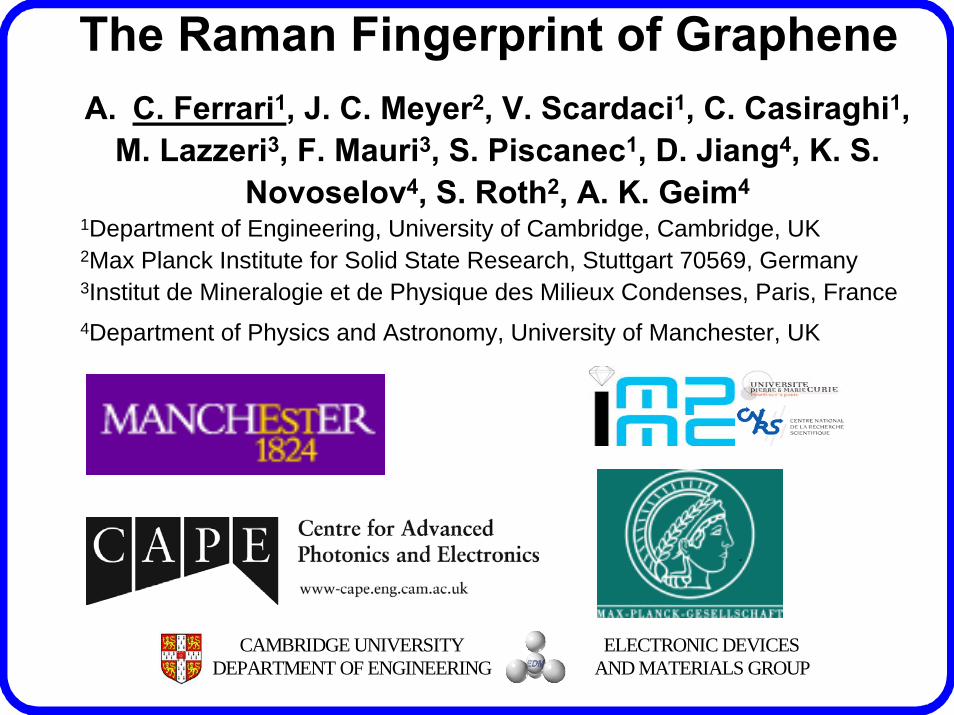
NanoTube-Evolution-Nagano 06
CAMBRIDGE UNIVERSITYDEPARTMENT OF ENGINEERING
ELECTRONIC DEVICES AND MATERIALS GROUP
NanoTube-Evolution-Nagano 06
“Cut…. Get graphene”Eklund-Sensei NT06
“Press (50GPa)…Get Diamond-like Carbon!”
S. Saito-Sensei CCNT06

CAMBRIDGE UNIVERSITYDEPARTMENT OF ENGINEERING
ELECTRONIC DEVICES AND MATERIALS GROUP
Graphene
•Electron transport described by the (relativistic-like) Dirac equation Access to the rich and subtle physics of quantum electrodynamics in a relatively simple condensed matter experiment
•Scalability of graphene devices to true nanometre dimensions makes it a promising candidate for future electronic applications, because of its ballistic transport at room temperature combined with chemical and mechanical stability.
•Graphene is the two-dimensional (2d) building block for carbon allotropes of every other dimensionality
….big hype recently…

CAMBRIDGE UNIVERSITYDEPARTMENT OF ENGINEERING
ELECTRONIC DEVICES AND MATERIALS GROUP
Transistor: Graphene Ribbon

CAMBRIDGE UNIVERSITYDEPARTMENT OF ENGINEERING
ELECTRONIC DEVICES AND MATERIALS GROUP
Drawing:(micro) mechanical cleavage of graphite
How to Make Graphene?

CAMBRIDGE UNIVERSITYDEPARTMENT OF ENGINEERING
ELECTRONIC DEVICES AND MATERIALS GROUPindividual atomic sheets: do they exist?
How to Make Graphene?
GRAPHITE ISSTRONGLY LAYERED
SLICE DOWN TO ONE ATOMIC PLANE

CAMBRIDGE UNIVERSITYDEPARTMENT OF ENGINEERING
ELECTRONIC DEVICES AND MATERIALS GROUP1 μm
SEM
1 μm
0Å 9Å 13Å
Free-Standing GrapheneAFM
1 μm
single layer of atoms visible by “naked” eyeonly on 300 nm SiO2
OPTICS
Key: Visual Identification

CAMBRIDGE UNIVERSITYDEPARTMENT OF ENGINEERING
ELECTRONIC DEVICES AND MATERIALS GROUP
HoweverNeed Extremely
Good Eye To Spot!!!
Single Layer

CAMBRIDGE UNIVERSITYDEPARTMENT OF ENGINEERING
ELECTRONIC DEVICES AND MATERIALS GROUP
TwoLayers

CAMBRIDGE UNIVERSITYDEPARTMENT OF ENGINEERING
ELECTRONIC DEVICES AND MATERIALS GROUP
One Comment…
However…Low yield, messy, not scalable
Better to grow graphenedirectly on substrate
This can be done…But…not the subject of this talk
Mechanical cleavage is nice and simple

CAMBRIDGE UNIVERSITYDEPARTMENT OF ENGINEERING
ELECTRONIC DEVICES AND MATERIALS GROUP
Another Comment
AFM thickness of single layer is0.5-1.5 nm! Due to chemical contrast
We want to be 150% sure
TEM

CAMBRIDGE UNIVERSITYDEPARTMENT OF ENGINEERING
ELECTRONIC DEVICES AND MATERIALS GROUP
Free-Hanging graphene sheets
500nm
1 layer of graphene !
J. C. Meyer

CAMBRIDGE UNIVERSITYDEPARTMENT OF ENGINEERING
ELECTRONIC DEVICES AND MATERIALS GROUP
Preparation1. Graphene sheet on substrate
2µm
2. Metal grid patterned ontothe flake
10µm

CAMBRIDGE UNIVERSITYDEPARTMENT OF ENGINEERING
ELECTRONIC DEVICES AND MATERIALS GROUP
Preparation
3. Etching of substrate
10µmFlake remainsin metal grid
4. TEM and electron diffraction analysis
500nm

CAMBRIDGE UNIVERSITYDEPARTMENT OF ENGINEERING
ELECTRONIC DEVICES AND MATERIALS GROUP
Electron diffraction:
Highly crystalline samples
Number of layers?Diffraction tilt series!

CAMBRIDGE UNIVERSITYDEPARTMENT OF ENGINEERING
ELECTRONIC DEVICES AND MATERIALS GROUP
Sheets fold back at the edges, and sometimes show a wrinkle within the sheet. HRTEM analysis of the folding allows to verify the layer count.
2nm
2nm
One-layer graphene

CAMBRIDGE UNIVERSITYDEPARTMENT OF ENGINEERING
ELECTRONIC DEVICES AND MATERIALS GROUP
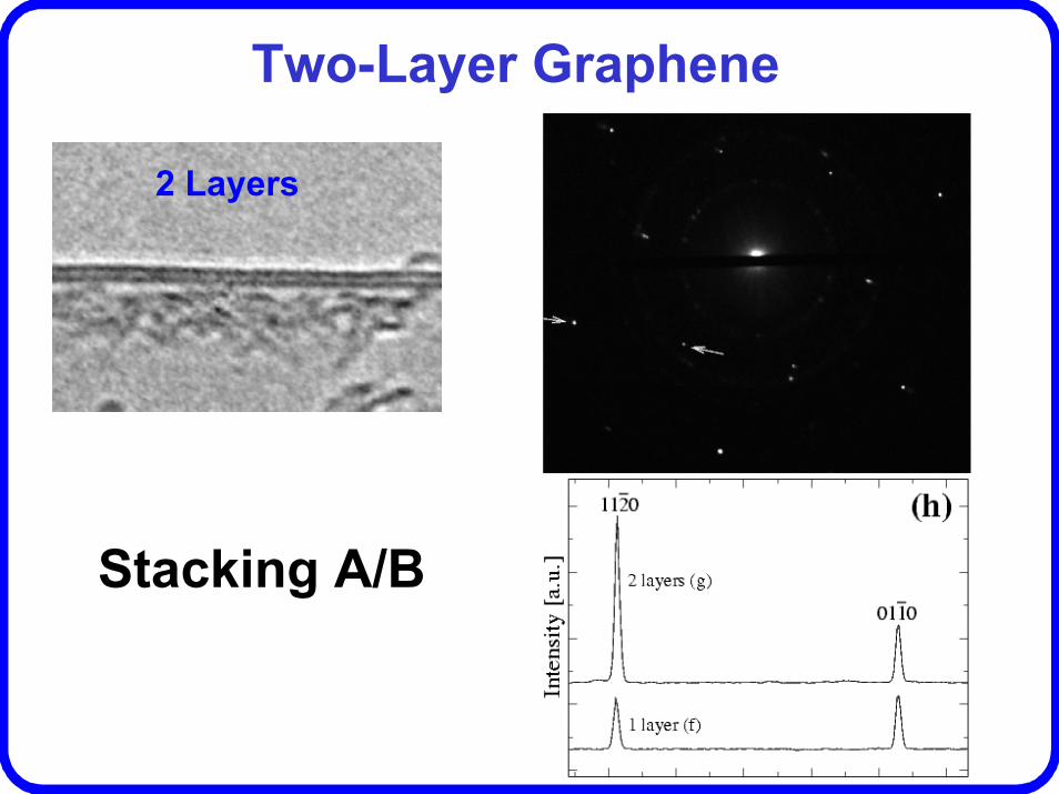
Two-layer graphene
2nm
CAMBRIDGE UNIVERSITYDEPARTMENT OF ENGINEERING
ELECTRONIC DEVICES AND MATERIALS GROUP
Two-Layer Graphene
2 Layers
Stacking A/B

CAMBRIDGE UNIVERSITYDEPARTMENT OF ENGINEERING
ELECTRONIC DEVICES AND MATERIALS GROUP
8 layers

CAMBRIDGE UNIVERSITYDEPARTMENT OF ENGINEERING
ELECTRONIC DEVICES AND MATERIALS GROUP
We Need High Throughput Non Destructive
Quick Substrate Independent
Identification Technique
Raman Spectroscopy

CAMBRIDGE UNIVERSITYDEPARTMENT OF ENGINEERING
ELECTRONIC DEVICES AND MATERIALS GROUP
1500 2000 2500 3000
Inte
nsity
Raman shift (cm-1)
514nm
Graphene
Graphite

CAMBRIDGE UNIVERSITYDEPARTMENT OF ENGINEERING
ELECTRONIC DEVICES AND MATERIALS GROUP
2500 2600 2700 2800 2900 30000
10000
20000
30000
40000
Graphene
Inte
nsity
(a. u
.)
Raman shift (cm-1)
514 nm
Graphite G’ Peak
(2D peak)
Clear Fingerprint

CAMBRIDGE UNIVERSITYDEPARTMENT OF ENGINEERING
ELECTRONIC DEVICES AND MATERIALS GROUP
1800 2400
Inte
nsity
(A.U
.)
Raman Shift (cm-1)
Graphene
1200 1300 1400 1500 1600 1700 1800
Inte
nsity
(A.U
.)
Raman Shift (cm-1)

CAMBRIDGE UNIVERSITYDEPARTMENT OF ENGINEERING
ELECTRONIC DEVICES AND MATERIALS GROUP
1800 2400
Inte
nsity
(A.U
.)
Raman Shift (cm-1)
Graphene
1200 1300 1400 1500 1600 1700 1800
Inte
nsity
(A.U
.)
Raman Shift (cm-1)
D peak intensityNOT related to Number of Layers
Disorder (in the widest possible meaning)
See Tuinstra Koening 1970…

CAMBRIDGE UNIVERSITYDEPARTMENT OF ENGINEERING
ELECTRONIC DEVICES AND MATERIALS GROUP
1500 2000 2500 3000
Inte
nsity
(A.U
.)
Raman Shift (cm-1)
Graphene
On Substrate
Suspended

CAMBRIDGE UNIVERSITYDEPARTMENT OF ENGINEERING
ELECTRONIC DEVICES AND MATERIALS GROUP
1500 2000 2500 3000
Inte
nsity
(A.U
.)
Raman Shift (cm-1)
2-Layers
514 nm
2600 2640 2680 2720 2760 2800
Inte
nsity
(A.U
.)
Raman Shift (cm-1)

CAMBRIDGE UNIVERSITYDEPARTMENT OF ENGINEERING
ELECTRONIC DEVICES AND MATERIALS GROUP
1500 1550 1600 16501500 1550 1600 1650
10 layers
5 layers
Inte
nsity
(a. u
.)
Raman shift (cm-1)
1 layer
2 layers
graphite
Raman shift (cm-1)
514nm 633 nm
Slight Upshift ~ 5cm-1

CAMBRIDGE UNIVERSITYDEPARTMENT OF ENGINEERING
ELECTRONIC DEVICES AND MATERIALS GROUP
2600 2700 28002600 2700 2800
10 layers
5 layers
2 layers
Inte
nsity
(a. u
.)
Raman shift (cm-1)
1 layer
graphite
514nm
633 nm
Raman shift (cm-1)

CAMBRIDGE UNIVERSITYDEPARTMENT OF ENGINEERING
ELECTRONIC DEVICES AND MATERIALS GROUP
2550 2600 2650 2700 2750 28000
5000
10000
15000
200002D2B2D2A
2D1A
Inte
nsity
(A.U
.)
Raman Shift (cm-1)
E) 2 Layer
514.5 nm
633 nm
2D1B
1300 1350 14000
500
1000
1500
2000
2500Edge Graphite
D2
Inte
nsity
(A. U
.)
Raman Shift (cm-1)
D
D) 514.5 nm
D1
Edge 1 Layer

CAMBRIDGE UNIVERSITYDEPARTMENT OF ENGINEERING
ELECTRONIC DEVICES AND MATERIALS GROUP
The Origin of G’ (2D) Peak
BUT it is the second order of D peak
Nothing to do with G peak
Named G’ since is one of the 2 biggest peaks in graphite
D forbidden in perfect crystal By Raman Fundamental Selection Rule q~0
However 2nd order always allowed: q+(-q)=0

CAMBRIDGE UNIVERSITYDEPARTMENT OF ENGINEERING
ELECTRONIC DEVICES AND MATERIALS GROUP
D Peak Dispersion Vidano et al. (1981)
Pocsik et al. (1998)

CAMBRIDGE UNIVERSITYDEPARTMENT OF ENGINEERING
ELECTRONIC DEVICES AND MATERIALS GROUP
Active by double resonance(Baranov 1988, Thomsen-Reich 2000)
D peak comes from LO phonons(Ferrari Robertson 2000)
Strongly dispersive due to Kohn Anomaly at K(Piscanec et al. 2004)

CAMBRIDGE UNIVERSITYDEPARTMENT OF ENGINEERING
ELECTRONIC DEVICES AND MATERIALS GROUP
Second order no defect scattering necessary
However…
In principle ALL phonons activeBUT
Double resonant phonons enhanced due to resonance and strong
electron-phonon coupling

CAMBRIDGE UNIVERSITYDEPARTMENT OF ENGINEERING
ELECTRONIC DEVICES AND MATERIALS GROUP
Previous double resonance modelspredict multiple D peaks for graphene
Double structure of 2D peak in graphitenever explained
Traditional interpretation (1980)2 Maxima in graphite
Phonon Density of States at K and MWRONG since 2D disperses with excitation
KEY: Evolution of Electron Bands with number of layers
in contrast with experiments

CAMBRIDGE UNIVERSITYDEPARTMENT OF ENGINEERING
ELECTRONIC DEVICES AND MATERIALS GROUP
Three Possible Processes
However: only 1 contributes

CAMBRIDGE UNIVERSITYDEPARTMENT OF ENGINEERING
ELECTRONIC DEVICES AND MATERIALS GROUP
Three Possible Processes
However: only 1 contributes
Small:Trigonal Warping
Forbidden:EPC=0
OK!

CAMBRIDGE UNIVERSITYDEPARTMENT OF ENGINEERING
ELECTRONIC DEVICES AND MATERIALS GROUP
Trigonal Warping Effect
• q > K Strong EPC and large portion of the phase-space • q < K Strong EPC but small portion of the phase-space • q ~ K EPC~0
Adapted from: Kurti et al., Phys. Rev. B 65 165433 (2002)

CAMBRIDGE UNIVERSITYDEPARTMENT OF ENGINEERING
ELECTRONIC DEVICES AND MATERIALS GROUP
1 Component D and 2D peaks
2500 2600 2700 2800 2900 3000
Graphene
Inte
nsity
(a. u
.)Raman shift (cm-1)
514 nm2D
1 3 0 0 1 3 5 0 1 4 0 0
Inte
nsity
(A. U
.)
R a m a n S h if t (c m -1 )
5 1 4 .5 n m
E d g e 1 L a y e r
D

CAMBRIDGE UNIVERSITYDEPARTMENT OF ENGINEERING
ELECTRONIC DEVICES AND MATERIALS GROUP
0.8 0.7 0.6 0.5
1300
1320
1340
1360
1380
1400
1420
Μ Κ Γ
q = (ξ,0,0)
ve Vector (2π/a0)
Two-layer GrapheneTwo possibilities:
1) Phonon Splitting
2) Band splitting
Phonon SplittingK-M is Minor
PRL 93, 185503 (2004)

CAMBRIDGE UNIVERSITYDEPARTMENT OF ENGINEERING
ELECTRONIC DEVICES AND MATERIALS GROUP
Band Splitting Main Effect
2550 2600 2650 2700 2750 28000
5000
10000
15000
200002D2B2D2A
2D1A
Inte
nsity
(A.U
.)
Raman Shift (cm-1)
2 Layer
514.5 nm
633 nm
2D1B
4 components2 Most intense

CAMBRIDGE UNIVERSITYDEPARTMENT OF ENGINEERING
ELECTRONIC DEVICES AND MATERIALS GROUP
Origin of Small Upshift of G peak
1 5 0 0 1 5 5 0 1 6 0 0 1 6 5 0
Inte
nsity
(a. u
.)
R a m a n sh ift (cm -1 )
1 la ye r
g ra p h ite
-0.1 0.0 0.11570
1580
1590
1600
q = (0,ξ,0)
Γ
~5 cm-1 Upshift
IRRaman GrapheneRaman Graphite
PRL 93, 185503 (2004)
Kohn Anomaly

CAMBRIDGE UNIVERSITYDEPARTMENT OF ENGINEERING
ELECTRONIC DEVICES AND MATERIALS GROUP
Phonon-Linewidths and EPCIn a perfect crystal, phonon linewidths determined byInteraction with other elementary excitations:
EPCan γγγ +=γan : anharmonic contribution, due to interactionWith other phonons. Determined by anharmonicterms in interatomic potential.
γEPC: interaction with electron-hole pairs. Determinedby EPC and present in systems with null electron gap
CAMBRIDGE UNIVERSITYDEPARTMENT OF ENGINEERING
ELECTRONIC DEVICES AND MATERIALS GROUP
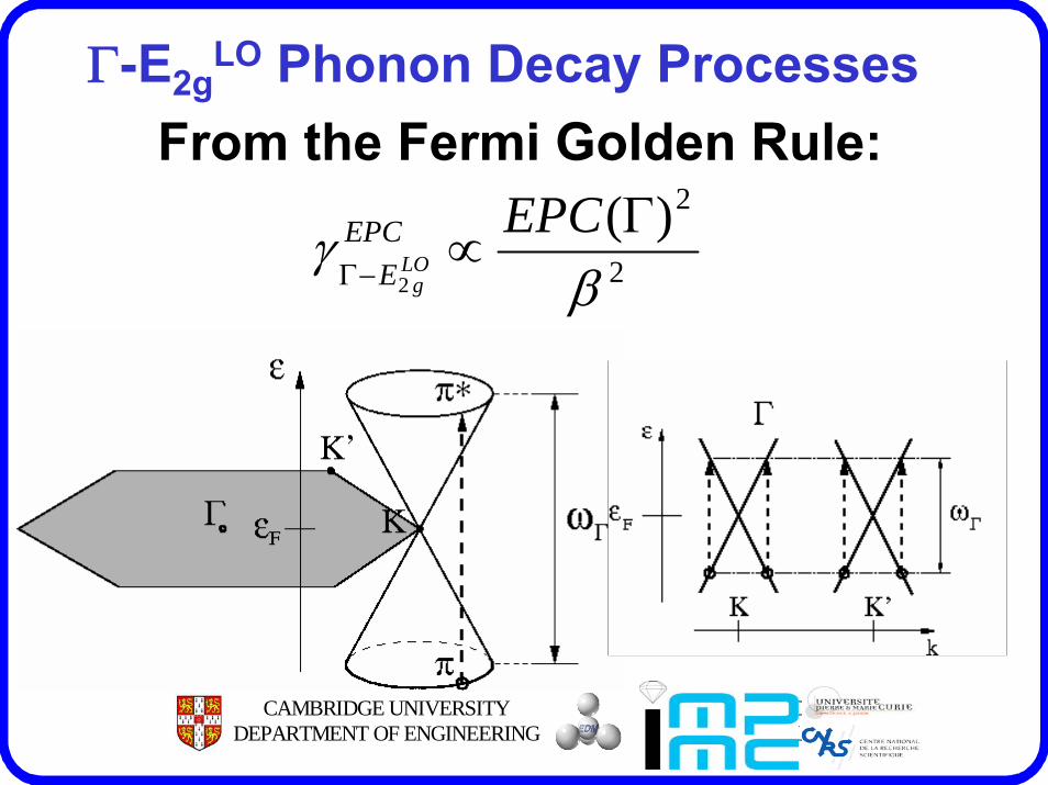
Γ-E2gLO Phonon Decay Processes
From the Fermi Golden Rule:
2
2)(2 β
γ Γ∝
−Γ
EPCEPCE LO
g

CAMBRIDGE UNIVERSITYDEPARTMENT OF ENGINEERING
ELECTRONIC DEVICES AND MATERIALS GROUP
Γ-E2gLO : Graphite Raman G Peak
1000 1200 1400 1600 1800 2000
Inte
nsity
(A. U
.)
Raman Shift (cm-1)
FWHM(G)= 13.5 cm-1
Single Crystal Graphite
No D Peak
No extra broadening due to disorder
No FWHM(G) increase with temperature
γan≤1.5 cm-1
(spectrometer resolution)
EPC(Γ)=45.5 (eV/Ą)2

CAMBRIDGE UNIVERSITYDEPARTMENT OF ENGINEERING
ELECTRONIC DEVICES AND MATERIALS GROUP
And… Single layer graphene…
1200 1400 1600 1800 2000
FWHM(G)= 14 cm-1
Inte
nsity
(A.U
.)
Raman Shift (cm-1)
Similar EPC
PRB 73, 155426 (2006)

CAMBRIDGE UNIVERSITYDEPARTMENT OF ENGINEERING
ELECTRONIC DEVICES AND MATERIALS GROUP
Implications for NanotubesSingle 2D peak graphene ⇒
Single 2D peak in Single Wall CNT
Curvature and confinement give diameter dependence
2D(SWNT)~2D (graphene)- A/d
2D position in Graphite should not be used to scale
Distribution of SWNTs of different diameters, distribution of 2D peaks

CAMBRIDGE UNIVERSITYDEPARTMENT OF ENGINEERING
ELECTRONIC DEVICES AND MATERIALS GROUP
What about Multi-Wall?
First approximation each wall gives a 2D peak
DWNT two 2D peaks (inner and outer wall)
HOWEVER, inter-wall interactions Can change simple picture
Further splitting, Less peaks!
Details to follow…

CAMBRIDGE UNIVERSITYDEPARTMENT OF ENGINEERING
ELECTRONIC DEVICES AND MATERIALS GROUP
ConclusionsIdentified unique features of Raman spectrum, which fingerprintsgraphene amongst all other carbon allotropes.
The Raman spectrum evolution with increasing number of layers reflects the evolution of the electronic structure and electron-phonon interactions
Raman spectroscopy is a quick, high-throughput, non-destructive technique for the unambiguous identification of graphene layers.
Raman+Graphene is Good Fun!

CAMBRIDGE UNIVERSITYDEPARTMENT OF ENGINEERING
ELECTRONIC DEVICES AND MATERIALS GROUP
Funding:• EU FAMOUS & CANAPE project• Marie Curie Fellowship IHP-HPMT-CT-2000-00209• The Royal Society• EPSRC GR/S97620/01•The Leverhulme Trust
CPU:• HPCF, Cambridge UK• IDRIS, Orsay France

CAMBRIDGE UNIVERSITYDEPARTMENT OF ENGINEERING
ELECTRONIC DEVICES AND MATERIALS GROUP
Reference