The RAD6000MCTM System-on-Chip Microcontroller for ...
14
1 The RAD6000MC TM System-on-Chip Microcontroller for Spacecraft Avionics and Instrument Control Richard Berger, Laura Burcin, David Hutcheson, Jennifer Koehler, Marla Lassa, Myrna Milliser, David Moser, Dan Stanley, Randy Zeger BAE Systems 9300 Wellington Road Manassas, Va. 20110-4122 703-367-1809 [email protected] Ben Blalock, Mark Hale University of Tennessee 1508 Middle Way Drive Knoxville, Tennessee 37996 Abstract—A highly integrated system-on-chip is currently in development. Based on the flight-proven RAD6000 TM microprocessor, this mixed-signal microcontroller supports a wide variety of standard digital interfaces commonly used in spacecraft avionics. Multiple analog input and output channels are also provided. 12 The current RAD6000 computer is a veteran of many space missions, many of which are still in operation such as the Mars Exploration Rovers. An early implementation of IBM’s “Power” architecture, this superscalar RISC processor includes both fixed and floating point execution units. Several variations of the computer board were developed and a set of support ASICs and FPGAs exists for the processor. While some of the support chips change with the board implementation, the basic core function consisted of the processor, a bridge chip, SRAM or DRAM memory, and EEPROM. Several different backplane buses were supported, including Peripheral Component Interconnect (PCI) and Versa Module Europa (VME). The RAD6000 computer is supported by the Wind River Systems VxWorks operating system and the Green Hills compiler. The RAD6000MC microcontroller will be manufactured in BAE Systems’ 150nm radiation hardened CMOS technology with the RAD6000 processor in the form of a reusable core. In addition to the RAD6000 processor, the system-on-chip will include 192 KB of SRAM in 64 KB blocks, 32 KB of non-volatile chalcogenide-based C- RAM TM , a 64-bit external memory interface with error correction code (ECC), a SpaceWire router with four links and dual internal ports, redundant 1553 interfaces, a 64-bit PCI bus interface, a direct memory access (DMA) controller, digital discrete I/O, a UART, a 2 nd smaller control processor called the embedded microcontroller (EMC), JTAG master and slave controllers for test, a 12-bit analog-to-digital converter with up to 48 inputs via an analog multiplexer, and three channels of 12-bit digital-to- 1 1 1-4244-1488-1/08/$25.00 ©2008 IEEE. 2 IEEEAC paper #1560, Version 3, Updated January 9, 2008 analog converter. All of these functions have been implemented as reusable cores, many of which are already flight-proven, and connect via a standard connection medium called the on-chip bus (OCB). The OCB is a non- blocking cross-bar switch with both high performance 64- bit and lower performance 32-bit buses. Parity is provided on the OCB for additional fault tolerance. The RAD6000MC will support operation up through 66 MHz for high throughput, but can also be operated at 33 MHz for lower power dissipation. The SpaceWire interfaces run at 300 MHz using a dedicated phase locked loop (PLL). The PCI interface will support 33 MHz on a PCI backplane. The RAD6000MC is being designed to be able to support a wide variety of applications, including that of a fully capable flight computer. It is also quite well suited for instrument control, and can be used in a large system with a distributed architecture. Existing RAD6000 software and test infrastructure will be reusable. This paper will discuss the RAD6000MC architecture, porting of the RAD6000 processor into a reusable core, development of the analog circuitry and analog control interface core, and various applications for which the RAD6000MC is well matched. TABLE OF CONTENTS 1. INTRODUCTION ..................................................... 2 2. RAD6000 MICROPROCESSOR ARCHITECTURE... 2 3. TRANSLATION OF THE RAD6000 TO VHDL ....... 2 4. RAD6000 CIRCUITRY .......................................... 4 5. THE ON CHIP BUS CONNECTION MEDIUM .......... 4 6. CONNECTING THE RAD6000 TO THE OCB ......... 4 7. MEMORY CORES................................................... 6 8. THE EMBEDDED MICROCONTROLLER................. 7 9. DIGITAL INTERFACE CORES ................................ 7 10. ANALOG CIRCUITRY AND INTERFACES ............. 8 11. RH15 RADIATION HARDENED CMOS............... 9 12. RAD6000MC SOFTWARE SUPPORT ................ 10
Transcript of The RAD6000MCTM System-on-Chip Microcontroller for ...

1
The RAD6000MCTM System-on-Chip Microcontroller for Spacecraft Avionics and Instrument Control
Richard Berger, Laura Burcin, David Hutcheson, Jennifer Koehler, Marla Lassa, Myrna Milliser, David Moser, Dan Stanley, Randy Zeger BAE Systems
9300 Wellington Road Manassas, Va. 20110-4122
703-367-1809 [email protected]
Ben Blalock, Mark Hale University of Tennessee 1508 Middle Way Drive
Knoxville, Tennessee 37996 Abstract—A highly integrated system-on-chip is currently in development. Based on the flight-proven RAD6000TM microprocessor, this mixed-signal microcontroller supports a wide variety of standard digital interfaces commonly used in spacecraft avionics. Multiple analog input and output channels are also provided. 12
The current RAD6000 computer is a veteran of many space missions, many of which are still in operation such as the Mars Exploration Rovers. An early implementation of IBM’s “Power” architecture, this superscalar RISC processor includes both fixed and floating point execution units. Several variations of the computer board were developed and a set of support ASICs and FPGAs exists for the processor. While some of the support chips change with the board implementation, the basic core function consisted of the processor, a bridge chip, SRAM or DRAM memory, and EEPROM. Several different backplane buses were supported, including Peripheral Component Interconnect (PCI) and Versa Module Europa (VME). The RAD6000 computer is supported by the Wind River Systems VxWorks operating system and the Green Hills compiler.
The RAD6000MC microcontroller will be manufactured in BAE Systems’ 150nm radiation hardened CMOS technology with the RAD6000 processor in the form of a reusable core. In addition to the RAD6000 processor, the system-on-chip will include 192 KB of SRAM in 64 KB blocks, 32 KB of non-volatile chalcogenide-based C-RAMTM, a 64-bit external memory interface with error correction code (ECC), a SpaceWire router with four links and dual internal ports, redundant 1553 interfaces, a 64-bit PCI bus interface, a direct memory access (DMA) controller, digital discrete I/O, a UART, a 2nd smaller control processor called the embedded microcontroller (EMC), JTAG master and slave controllers for test, a 12-bit analog-to-digital converter with up to 48 inputs via an analog multiplexer, and three channels of 12-bit digital-to-
1 1 1-4244-1488-1/08/$25.00 ©2008 IEEE. 2 IEEEAC paper #1560, Version 3, Updated January 9, 2008
analog converter. All of these functions have been implemented as reusable cores, many of which are already flight-proven, and connect via a standard connection medium called the on-chip bus (OCB). The OCB is a non-blocking cross-bar switch with both high performance 64-bit and lower performance 32-bit buses. Parity is provided on the OCB for additional fault tolerance.
The RAD6000MC will support operation up through 66 MHz for high throughput, but can also be operated at 33 MHz for lower power dissipation. The SpaceWire interfaces run at 300 MHz using a dedicated phase locked loop (PLL). The PCI interface will support 33 MHz on a PCI backplane.
The RAD6000MC is being designed to be able to support a wide variety of applications, including that of a fully capable flight computer. It is also quite well suited for instrument control, and can be used in a large system with a distributed architecture. Existing RAD6000 software and test infrastructure will be reusable.
This paper will discuss the RAD6000MC architecture, porting of the RAD6000 processor into a reusable core, development of the analog circuitry and analog control interface core, and various applications for which the RAD6000MC is well matched.
TABLE OF CONTENTS
1. INTRODUCTION ..................................................... 2 2. RAD6000 MICROPROCESSOR ARCHITECTURE... 2 3. TRANSLATION OF THE RAD6000 TO VHDL ....... 2 4. RAD6000 CIRCUITRY .......................................... 4 5. THE ON CHIP BUS CONNECTION MEDIUM.......... 4 6. CONNECTING THE RAD6000 TO THE OCB ......... 4 7. MEMORY CORES................................................... 6 8. THE EMBEDDED MICROCONTROLLER................. 7 9. DIGITAL INTERFACE CORES ................................ 7 10. ANALOG CIRCUITRY AND INTERFACES ............. 8 11. RH15 RADIATION HARDENED CMOS............... 9 12. RAD6000MC SOFTWARE SUPPORT ................ 10

2
13. SPACE PLUG AND PLAY ASIM APPLICATION ..10 14. ADDITIONAL APPLICATIONS.............................10 15. POWER OPTIMIZATION FOR APPLICATIONS ....11 16. RAD6000MC PERFORMANCE..........................11 17. SUMMARY..........................................................12 REFERENCES ...........................................................12 BIOGRAPHIES ..........................................................13
1. INTRODUCTION
The introduction of advanced 150 nm radiation hardened technology opens new opportunities for extremely high levels of integration, enabling the development of true system-on-chip solutions. Only a little more than a decade ago, the RAD6000 represented the state-of-the-art in spaceborne processing. A design ported from IBM’s “Power” RISC/System 6000TM architecture, the RAD6000 was built in 0.5 micron technology as a standalone ASIC with circuitry modified to resist single-event upsets for reliable spaceborne operation. The single board computers used on many space missions combined this processor chip with an entire family of support ASICs and/or FPGAs, and additional boards were employed for some mission-specific I/O functions. The RAD6000MC employs the very same RAD6000 design, now migrated to 150 nm technology where it can be combined with the family chip functions and a combination of both digital and analog interfaces, all within a single die.
Some of the limitations of the early architecture have been addressed in this new design and care has been taken to minimize the possibility of throughput bottlenecks given the massively integrated nature of the ASIC. The RAD6000 processor has been combined with a variety of digital serial and parallel interface and both analog inputs and outputs to create a large mixed-signal ASIC that extends the breadth of circuitry and the reusable core library often employed in the development of ASICs by BAE Systems.
The goal of the RAD6000MC ASIC is to be able to provide all of the capabilities required to control an instrument or to act as the flight computer for a small spacecraft either completely self contained, or with only the addition of some amount of external memory. Uplink and downlink functions have not been incorporated due to the variety of protocols being employed for that purpose.
The RAD6000MC includes on-chip memory blocks of both SRAM and a C-RAMTM non-volatile memory based on the use of chalcogenide material for the memory element. There are several blocks of SRAM, to prevent contention for access to memory by the various interfaces. Access to external memory is provided via a separate core. A second RISC processor called the embedded microcontroller (EMC) is also included. It supplements the RAD6000 and assists in initial booting of the chip. Digital interfaces include redundant MIL-STD-1553B interfaces, a 64-bit PCI
bus, and a SpaceWire router with four links. Analog interfaces include a 12-bit A/D converter with an integrated programmable analog multiplexer as well as 3 channels of 12-bit D/A conversion.
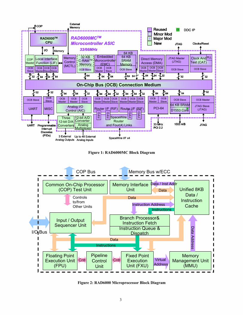
All of these functions have been designed as reusable cores and are connected to the on-chip bus. As shown below in Figure 1, many of the cores are completely reused, and others have been only slightly modified for this design. The analog circuitry is brand new.
2. RAD6000 MICROPROCESSOR ARCHITECTURE
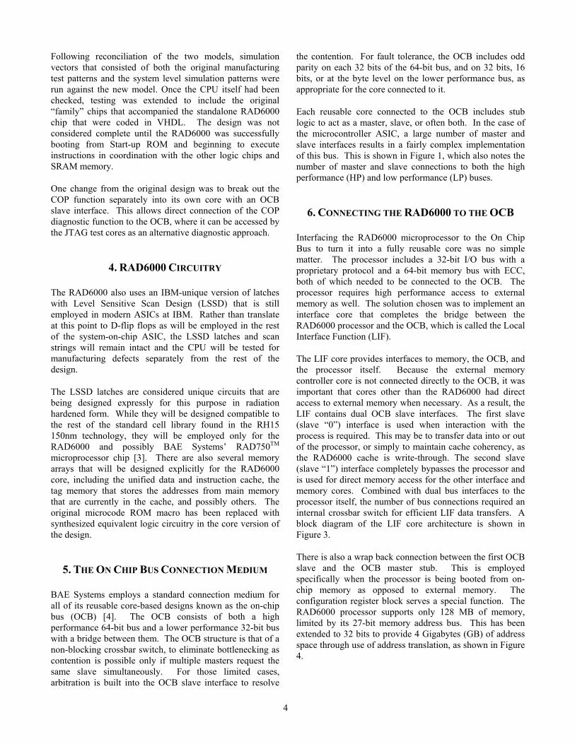
The RAD6000 [1] is a superscalar reduced instruction set computer (RISC) with both fixed point and floating point execution units, as shown in Figure 2. The processor is capable of issuing up to three instructions per cycle: fixed-point, floating-point, and a branch. A two-way set associative unified 8 Kilobyte (KB) cache is supported by a memory management unit. There are separate memory and I/O buses. The memory bus is 64 bits of data plus 8 bits of error correction code (ECC) and has a 27-bit address bus to support up to 128 Megabytes (MB) of main system memory. The I/O bus is 32 bits wide. A separate common on-chip processor (COP) function was provided for diagnostic purposes, supported by an IBM diagnostic tool with hardware and software elements known as RISCWatch.
Software support of the RAD6000 is provided by the VxWorks real-time operating system from Wind River and the Green Hills C compiler. BAE Systems also provides a board support package with each RAD6000-based system.
3. TRANSLATION OF THE RAD6000 TO VHDL
The RAD6000 was based on the RISC single chip (RSC) that was developed in 1990 [2]. At that time, IBM employed unique design languages to describe both the behavioral and gate level models of its chips. We chose to transfer the RAD6000 to the VHDL language at the gate level from the IBM proprietary language known as Basic Design Language for Structures (BLD/S).
Because there are no commercial EDA tools that allow for Boolean comparison between this language and VHDL, and decision was made to independently translate two versions of the design: the original BDL/S code and a variant developed for use with a Zycad hardware accelerator that is no longer in operation. The BDL/S code had been used for manufacturing test patterns and the Zycad model (in yet another language) had been used for system level testing at the board level. Once two independent models had been generated in VHDL, they were reconciled through use of the Formality boolean comparison tool from Synopsys.
3
On-Chip Bus (OCB) Connection Medium
Embedded Microcontroller
(EMC)
64
OCB Master
64
OCB Slave
64 KB SRAM
MemoryOCB Slave
64 KB SRAM
MemoryOCB Slave
6464
Programmable Interrupt Discretes
(PIDs)
MISC
32
OCB Slave
JTAG
32
OCB Slave
JTAG Master (JTAG)
33 MHz PCI 2.2
64 64
OCB Master
OCB Slave
PCI-64
Clocks/Reset
Clock And Test (CAT)
32
PLL
OCB Slave
JTAG
32
OCB Master
JTAG Slave (JTAG)
Memory
RAD6000MCTM
Microcontroller ASICI/O
RAD6000TM
CPU
COP
OCB Slave
32
COP Master
33/66MHz
1553 A/B
64
OCB Slave
D1553 Core64 KB SRAM
UART
UART
32
OCB Slave
Up to 48 External Analog Inputs
Analog Multiplexer
12-bit A/DConverter
OCB Master
OCB Slave
64 3264
Analog I/O Control (AIC)
OCB Master
Three 12-bit D/A Converters
3 External Analog Outputs
SpaceWire Router
and Four(4) Links
SpaceWire I/F x4
64
OCB Master
32
OCB Slave
64
Router I/F (RIF)
OCB Master
FIFO
FIFO
OCB Master
OCB Slave
64 3264
Router I/F (RIF)
OCB Master
FIFO
FIFO
32 KB C-RAMTM
Memory
64
OCB Slave
Reused
New
Minor ModMajor Mod
DDC IP
External Memory
Memory Control (MCTL)
64 3264
OCB Master
OCB Slave
OCB Master
Direct Memory Access (DMA)
Local Interface Function (LIF)
64
OCB Slave
OCB Master
64 64
OCB Slave
On-Chip Bus (OCB) Connection MediumOn-Chip Bus (OCB) Connection Medium
Embedded Microcontroller
(EMC)
64
OCB Master
64
OCB Slave
Embedded Microcontroller
(EMC)
64
OCB Master
64
OCB Slave
64 KB SRAM
MemoryOCB Slave
64 KB SRAM
MemoryOCB Slave
6464
64 KB SRAM
MemoryOCB Slave
64 KB SRAM
MemoryOCB Slave
6464
Programmable Interrupt Discretes
(PIDs)
MISC
32
OCB Slave
Programmable Interrupt Discretes
(PIDs)
MISC
32
OCB Slave
JTAG
32
OCB Slave
JTAG Master (JTAG)
JTAG
32
OCB Slave
JTAG Master (JTAG)
33 MHz PCI 2.2
64 64
OCB Master
OCB Slave
PCI-64
33 MHz PCI 2.2
64 64
OCB Master
OCB Slave
64 64
OCB Master
OCB Slave
PCI-64
Clocks/Reset
Clock And Test (CAT)
32
PLL
OCB Slave
Clocks/Reset
Clock And Test (CAT)
32
PLL
OCB Slave
JTAG
32
OCB Master
JTAG Slave (JTAG)
JTAG
32
OCB Master
JTAG Slave (JTAG)
Memory
RAD6000MCTM
Microcontroller ASICI/O
RAD6000TM
CPU
COP
OCB Slave
32
COP Master
I/O
RAD6000TM
CPU
COP
OCB Slave
32
COP Master
33/66MHz
1553 A/B
64
OCB Slave
D1553 Core64 KB SRAM
1553 A/B
64
OCB Slave
D1553 Core64 KB SRAM
UART
UART
32
OCB Slave
UART
UART
32
OCB Slave
Up to 48 External Analog Inputs
Analog Multiplexer
12-bit A/DConverter
OCB Master
OCB Slave
64 3264 64 3264
Analog I/O Control (AIC)
OCB Master
Three 12-bit D/A Converters
3 External Analog Outputs
SpaceWire Router
and Four(4) Links
SpaceWire I/F x4
64
OCB Master
32
OCB Slave
64
Router I/F (RIF)
OCB Master
FIFO
FIFO
64
OCB Master
32
OCB Slave
64
Router I/F (RIF)
OCB Master
FIFO
FIFO
FIFO
FIFO
OCB Master
OCB Slave
64 3264
Router I/F (RIF)
OCB Master
FIFO
FIFO
OCB Master
OCB Slave
64 3264 64 3264
Router I/F (RIF)
OCB Master
FIFO
FIFO
FIFO
FIFO
32 KB C-RAMTM
Memory
64
OCB Slave
32 KB C-RAMTM
Memory
64
OCB Slave
Reused
New
Minor ModMajor Mod
ReusedReused
NewNew
Minor ModMinor ModMajor ModMajor Mod
DDC IP
External Memory
Memory Control (MCTL)
External Memory
Memory Control (MCTL)
64 3264
OCB Master
OCB Slave
OCB Master
Direct Memory Access (DMA)
64 3264
OCB Master
OCB Slave
OCB Master
Direct Memory Access (DMA)
OCB Master
OCB Slave
OCB Master
Direct Memory Access (DMA)
Local Interface Function (LIF)
64
OCB Slave
OCB Master
64 64
OCB Slave
Local Interface Function (LIF)
64
OCB Slave
OCB Master
64 64
OCB Slave
Figure 1: RAD6000MC Block Diagram
Unified 8KB Data /
Instruction Cache
Memory Interface Unit
Pipeline Control
Unit
Input / Output Sequencer Unit
Instruction Queue & Dispatch
Fixed Point Execution Unit (FXU)
Floating Point Execution Unit
(FPU)
Common On-Chip Processor (COP) Test Unit
Memory Management Unit
(MMU)
Memory Bus w/ECC
I/O Bus
Data / Inst Addr
Data
Cntl Virtual Address
Instructions
Data
Instruction Address
Data Address
Data Instructions
COP Bus
Controls to/fromOther Units
Branch Processor& Instruction Fetch
Cntl
Figure 2: RAD6000 Microprocessor Block Diagram
4
Following reconciliation of the two models, simulation vectors that consisted of both the original manufacturing test patterns and the system level simulation patterns were run against the new model. Once the CPU itself had been checked, testing was extended to include the original “family” chips that accompanied the standalone RAD6000 chip that were coded in VHDL. The design was not considered complete until the RAD6000 was successfully booting from Start-up ROM and beginning to execute instructions in coordination with the other logic chips and SRAM memory.
One change from the original design was to break out the COP function separately into its own core with an OCB slave interface. This allows direct connection of the COP diagnostic function to the OCB, where it can be accessed by the JTAG test cores as an alternative diagnostic approach.
4. RAD6000 CIRCUITRY
The RAD6000 also uses an IBM-unique version of latches with Level Sensitive Scan Design (LSSD) that is still employed in modern ASICs at IBM. Rather than translate at this point to D-flip flops as will be employed in the rest of the system-on-chip ASIC, the LSSD latches and scan strings will remain intact and the CPU will be tested for manufacturing defects separately from the rest of the design.
The LSSD latches are considered unique circuits that are being designed expressly for this purpose in radiation hardened form. While they will be designed compatible to the rest of the standard cell library found in the RH15 150nm technology, they will be employed only for the RAD6000 and possibly BAE Systems’ RAD750TM microprocessor chip [3]. There are also several memory arrays that will be designed explicitly for the RAD6000 core, including the unified data and instruction cache, the tag memory that stores the addresses from main memory that are currently in the cache, and possibly others. The original microcode ROM macro has been replaced with synthesized equivalent logic circuitry in the core version of the design.
5. THE ON CHIP BUS CONNECTION MEDIUM
BAE Systems employs a standard connection medium for all of its reusable core-based designs known as the on-chip bus (OCB) [4]. The OCB consists of both a high performance 64-bit bus and a lower performance 32-bit bus with a bridge between them. The OCB structure is that of a non-blocking crossbar switch, to eliminate bottlenecking as contention is possible only if multiple masters request the same slave simultaneously. For those limited cases, arbitration is built into the OCB slave interface to resolve
the contention. For fault tolerance, the OCB includes odd parity on each 32 bits of the 64-bit bus, and on 32 bits, 16 bits, or at the byte level on the lower performance bus, as appropriate for the core connected to it.
Each reusable core connected to the OCB includes stub logic to act as a master, slave, or often both. In the case of the microcontroller ASIC, a large number of master and slave interfaces results in a fairly complex implementation of this bus. This is shown in Figure 1, which also notes the number of master and slave connections to both the high performance (HP) and low performance (LP) buses.
6. CONNECTING THE RAD6000 TO THE OCB
Interfacing the RAD6000 microprocessor to the On Chip Bus to turn it into a fully reusable core was no simple matter. The processor includes a 32-bit I/O bus with a proprietary protocol and a 64-bit memory bus with ECC, both of which needed to be connected to the OCB. The processor requires high performance access to external memory as well. The solution chosen was to implement an interface core that completes the bridge between the RAD6000 processor and the OCB, which is called the Local Interface Function (LIF).
The LIF core provides interfaces to memory, the OCB, and the processor itself. Because the external memory controller core is not connected directly to the OCB, it was important that cores other than the RAD6000 had direct access to external memory when necessary. As a result, the LIF contains dual OCB slave interfaces. The first slave (slave “0”) interface is used when interaction with the process is required. This may be to transfer data into or out of the processor, or simply to maintain cache coherency, as the RAD6000 cache is write-through. The second slave (slave “1”) interface completely bypasses the processor and is used for direct memory access for the other interface and memory cores. Combined with dual bus interfaces to the processor itself, the number of bus connections required an internal crossbar switch for efficient LIF data transfers. A block diagram of the LIF core architecture is shown in Figure 3.
There is also a wrap back connection between the first OCB slave and the OCB master stub. This is employed specifically when the processor is being booted from on-chip memory as opposed to external memory. The configuration register block serves a special function. The RAD6000 processor supports only 128 MB of memory, limited by its 27-bit memory address bus. This has been extended to 32 bits to provide 4 Gigabytes (GB) of address space through use of address translation, as shown in Figure 4.

5
RAD6000 Memory I/F
RAD6000 Memory Bus
PIO I/F
RAD6000 I/O Bus
DMA I/F
Configuration Registers
OCB Master I/F OCB Slave (0) I/F
OCB Master Stub OCB Slave (0) Stub
Memory Configuration I/F
Memory Request I/F
Memory Controller MC Bus
Memory Controller Request Bus
OCB Slave (1) I/F
OCB Slave (1) Stub
Figure 3: Local Interface Function Block Diagram
RSC_MEM_ADDR (0:23)
3
ADDR (31:0)
Base Address Registers
(8) 16 MB Pages
Base Addr Attr
8 21 30’s
To OCB or Memory Controller
The complete address space is 4 GB, but the
available address space for the RAD6000 is 2 GB
The other 2 GB is dedicated for the other cores within the system
The complete RAD6000 (RSC) memory address bus
is 27 bits
Only the 24 most significant bits (MSBs) are brought out,
since the RAD6000 accesses 64-bit (8 byte)
words from memory
The 3 least significant bits (LSBs) are shown padded
below with zeros
Figure 4: RAD6000 Memory Address Translation
6
OCB_ADDR (31:0)
3 Bits (26:24)
ADDR (31:0)
Base Address Regs
(8) 16 MB Pages
Base Addr Attr
8 24
To RAD6000 I/O Bus, OCB, or Memory Controller
Bits (31:24)
Rd Snoop DisableWr Snoop Disable
For accesses within the 128 MB RAD6000 addressable region: The Attr field for that page determines if the access is snooped
Snooped accesses are passed directly to the RAD6000 (RSC) I/O Bus
Non-snooped accesses pick up the Base Addr field for the page and then are passed to
either the Memory Controller or OCB
For accesses above the 128 MB RAD6000 addressable region:
The address is passed directly to the Memory
Controller – no snooping
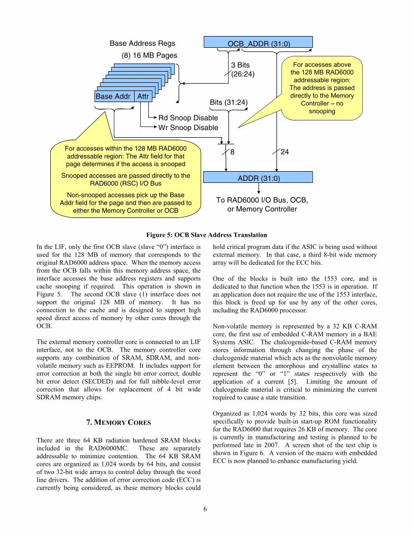
Figure 5: OCB Slave Address Translation
In the LIF, only the first OCB slave (slave “0”) interface is used for the 128 MB of memory that corresponds to the original RAD6000 address space. When the memory access from the OCB falls within this memory address space, the interface accesses the base address registers and supports cache snooping if required. This operation is shown in Figure 5. The second OCB slave (1) interface does not support the original 128 MB of memory. It has no connection to the cache and is designed to support high speed direct access of memory by other cores through the OCB.
The external memory controller core is connected to an LIF interface, not to the OCB. The memory controller core supports any combination of SRAM, SDRAM, and non-volatile memory such as EEPROM. It includes support for error correction at both the single bit error correct, double bit error detect (SECDED) and for full nibble-level error correction that allows for replacement of 4 bit wide SDRAM memory chips.
7. MEMORY CORES
There are three 64 KB radiation hardened SRAM blocks included in the RAD6000MC. These are separately addressable to minimize contention. The 64 KB SRAM cores are organized as 1,024 words by 64 bits, and consist of two 32-bit wide arrays to control delay through the word line drivers. The addition of error correction code (ECC) is currently being considered, as these memory blocks could
hold critical program data if the ASIC is being used without external memory. In that case, a third 8-bit wide memory array will be dedicated for the ECC bits.
One of the blocks is built into the 1553 core, and is dedicated to that function when the 1553 is in operation. If an application does not require the use of the 1553 interface, this block is freed up for use by any of the other cores, including the RAD6000 processor.
Non-volatile memory is represented by a 32 KB C-RAM core, the first use of embedded C-RAM memory in a BAE Systems ASIC. The chalcogenide-based C-RAM memory stores information through changing the phase of the chalcogenide material which acts as the nonvolatile memory element between the amorphous and crystalline states to represent the “0” or “1” states respectively with the application of a current [5]. Limiting the amount of chalcogenide material is critical to minimizing the current required to cause a state transition.
Organized as 1,024 words by 32 bits, this core was sized specifically to provide built-in start-up ROM functionality for the RAD6000 that requires 26 KB of memory. The core is currently in manufacturing and testing is planned to be performed late in 2007. A screen shot of the test chip is shown in Figure 6. A version of the macro with embedded ECC is now planned to enhance manufacturing yield.

7
Figure 6: Embedded C-RAM Test Chip
8. THE EMBEDDED MICROCONTROLLER
The embedded microcontroller (EMC) is a synthesizable 32-bit RISC processor core with a single fixed point execution unit and a 2 KB instruction cache. It includes 24 32-bit general purpose registers and 8 special purpose registers. The EMC processor architecture is unique to BAE Systems [6], and a C compiler has been developed to support generation of EMC code. The EMC is employed to control reset sequences for the RAD6000 processor, for housekeeping functions within the RAD6000MC ASIC, and for support of some reusable cores. As an example of this, code has already been written in support of the SpaceWire interface, creating descriptors to partition large data files to provide a more manageable downlink. A block diagram of the EMC is shown in Figure 7.
InstructionPre-fetch
Buffer
InstructionDecode
ExecutionUnit
SpecialPurposeRegisters
OCBSlave
Interface
OCBMaster
Interface
GeneralPurposeRegisters
OCB
VectorInterrupts
Figure 7: Embedded Microcontroller Block Diagram
The major components of the EMC development system consist of the C compiler, an EMC assembler, a linker, a
mapper and a debugger, and the CYGWIN “Linux” environment. A “make” facility is used to integrate these components.
9. DIGITAL INTERFACE CORES
There are three different standard digital interfaces within the RAD6000MC. The peripheral Component Interconnect (PCI) bus has been a backplane standard for onboard computers for several years, typically in a 32-bit, 33 MHz form. In the RAD6000MC, the PCI interface is extended to 64 bits, allowing for greater throughput across the bus and support version 2.2 of the PCI standard. The interface in this design supports 66 MHz when used within a card, but is still constrained to 33 MHz out on a CompactPCI®
backplane due to performance limitations associated with the required 8 cards and signal timing of the CompactPCI standard. Bus throughput @ 33 MHz is up to 264 MB per second. For higher fault tolerance, the PCI interface includes word level parity on the 32-bit address bus and on both words of the 64-bit data. The SpaceWire router is an improved version of the router incorporated into the BAE Systems’ SpaceWire ASIC [7]. The design is based on a synthesizable core developed at NASA Goddard Space Flight Center and integrated with the OCB as a joint design effort with BAE Systems. The router supports 4 SpaceWire links and dual parallel ports into the OCB. The links include on-chip LVDS I/O circuitry that support cold sparing for in-flight replacement. Time code is supported as well. The configuration port includes the routing table. In this version of the design, protocol ID has been added to support software implementation of the Remote Memory Access Protocol (RMAP) and the performance of both the time code and links have been improved. The die area required for the router has been decreased as well.
Unique functions of the BAE Systems SpaceWire router core include the following:
(1) the ability to limit maximum packet size to 1 MB to prevent bottlenecking in the network
(2) a bypass mode that allows a fixed routing assignment for the packet, ignoring the SpaceWire addressing for faster throughput when the destination is always known
(3) a local header byte that indicates the SpaceWire port from which the packet has been received and the presence of a logical address
A redundant MIL-STD-1553B interface has been developed that combines the use of the 1553 reusable core from Data Device Corporation (DDC) with an OCB interface and a 64 KB SRAM memory block. The DDC core supports Bus
8
Controller and Remote Terminal (BC/RT) functions and provides dual redundant links. This relatively low performance (1 Mb/s) serial bus has been the standard for guidance, navigation, and control (GNC) peripherals in many satellites.
10. ANALOG CIRCUITRY AND INTERFACES
The RAD6000MC includes a 12-bit pipelined analog-to-digital (A/D) converter with differential input that operates at 8.25 MHz. The A/D converter is combined with a programmable analog multiplexer that supports up to 48 single-ended inputs. A differential input Bandgap Reference (BGR) circuit also supports the A/D converter. The A/D converter implements a 1.5-bit per stage pipeline architecture that accepts a 4 V differential input where the input voltages swing 1 volt above or below the 1.95 V common mode reference. To support full resolution at a maximum of 10 Ms/s, the A/D converter employs a high accuracy sample and hold circuit. This circuit includes a folded cascade amplifier with four high-gain operational transconductance amplifiers (OTA). The OTAs are used as regulation amplifiers to enhance gain and minimize propagation of errors through the 11 stages of the A/D converter. Comparator errors up to 500 mV can be tolerated due to the incorporation of a digital error correction algorithm, decreasing sensitivity to single event particle induced errors.
While the RH15 technology employs a 1.5 V core, the A/D converter was constructed entirely out of the 3.3 V thicker oxide transistors typically used for I/O circuitry. This provided for the greatest dynamic range with a larger least significant bit, and also results in lower power dissipation than would be the case if the 1.5V transistors had been used. The A/D converter dissipates approximately 200 mW. If the application does not require the use of the A/D converter, or during periods when the A/D converter is not in operation, bias to the sample and hold amplifiers can be disabled via a small PMOS transistor within the current mirror of the A/D converter’s current bias circuit to reduce power.
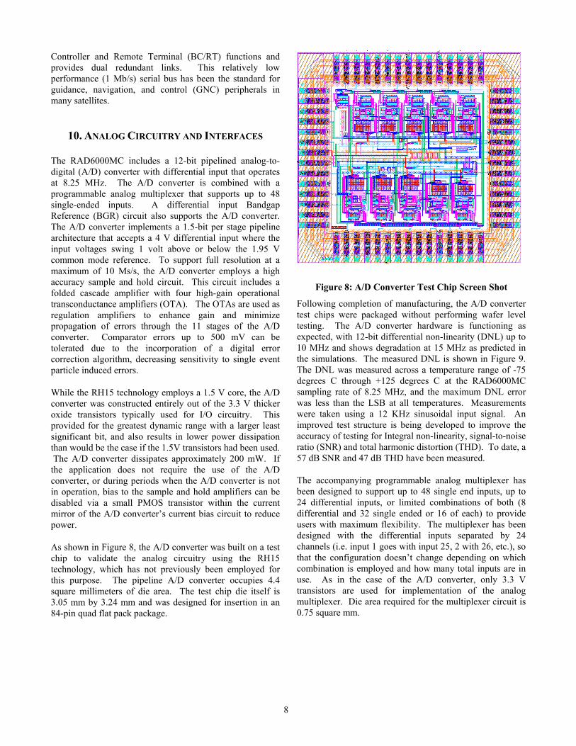
As shown in Figure 8, the A/D converter was built on a test chip to validate the analog circuitry using the RH15 technology, which has not previously been employed for this purpose. The pipeline A/D converter occupies 4.4 square millimeters of die area. The test chip die itself is 3.05 mm by 3.24 mm and was designed for insertion in an 84-pin quad flat pack package.
Figure 8: A/D Converter Test Chip Screen Shot
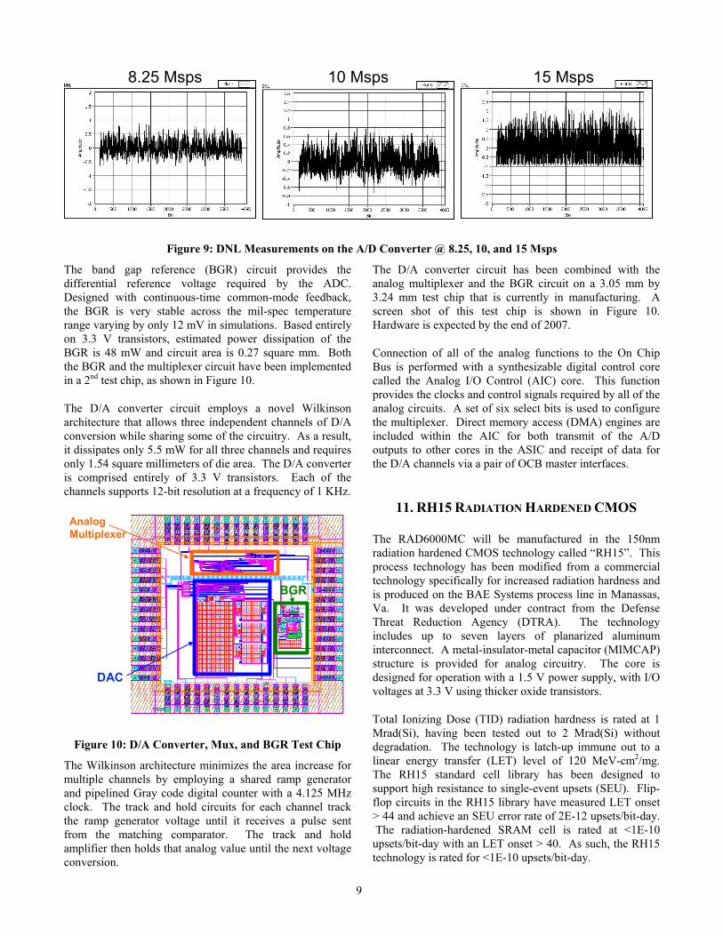
Following completion of manufacturing, the A/D converter test chips were packaged without performing wafer level testing. The A/D converter hardware is functioning as expected, with 12-bit differential non-linearity (DNL) up to 10 MHz and shows degradation at 15 MHz as predicted in the simulations. The measured DNL is shown in Figure 9. The DNL was measured across a temperature range of -75 degrees C through +125 degrees C at the RAD6000MC sampling rate of 8.25 MHz, and the maximum DNL error was less than the LSB at all temperatures. Measurements were taken using a 12 KHz sinusoidal input signal. An improved test structure is being developed to improve the accuracy of testing for Integral non-linearity, signal-to-noise ratio (SNR) and total harmonic distortion (THD). To date, a 57 dB SNR and 47 dB THD have been measured.
The accompanying programmable analog multiplexer has been designed to support up to 48 single end inputs, up to 24 differential inputs, or limited combinations of both (8 differential and 32 single ended or 16 of each) to provide users with maximum flexibility. The multiplexer has been designed with the differential inputs separated by 24 channels (i.e. input 1 goes with input 25, 2 with 26, etc.), so that the configuration doesn’t change depending on which combination is employed and how many total inputs are in use. As in the case of the A/D converter, only 3.3 V transistors are used for implementation of the analog multiplexer. Die area required for the multiplexer circuit is 0.75 square mm.
9
Figure 9: DNL Measurements on the A/D Converter @ 8.25, 10, and 15 Msps
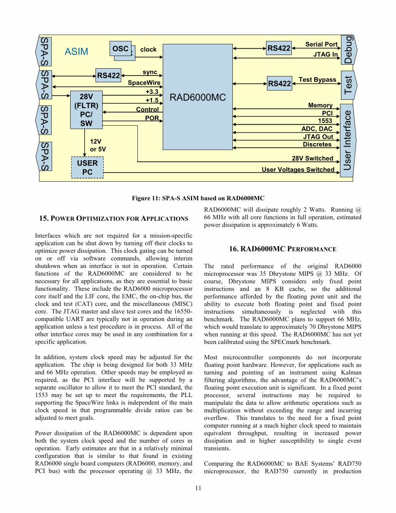
The band gap reference (BGR) circuit provides the differential reference voltage required by the ADC. Designed with continuous-time common-mode feedback, the BGR is very stable across the mil-spec temperature range varying by only 12 mV in simulations. Based entirely on 3.3 V transistors, estimated power dissipation of the BGR is 48 mW and circuit area is 0.27 square mm. Both the BGR and the multiplexer circuit have been implemented in a 2nd test chip, as shown in Figure 10.
The D/A converter circuit employs a novel Wilkinson architecture that allows three independent channels of D/A conversion while sharing some of the circuitry. As a result, it dissipates only 5.5 mW for all three channels and requires only 1.54 square millimeters of die area. The D/A converter is comprised entirely of 3.3 V transistors. Each of the channels supports 12-bit resolution at a frequency of 1 KHz.
BGR
DAC
Analog Multiplexer
Figure 10: D/A Converter, Mux, and BGR Test Chip
The Wilkinson architecture minimizes the area increase for multiple channels by employing a shared ramp generator and pipelined Gray code digital counter with a 4.125 MHz clock. The track and hold circuits for each channel track the ramp generator voltage until it receives a pulse sent from the matching comparator. The track and hold amplifier then holds that analog value until the next voltage conversion.
The D/A converter circuit has been combined with the analog multiplexer and the BGR circuit on a 3.05 mm by 3.24 mm test chip that is currently in manufacturing. A screen shot of this test chip is shown in Figure 10. Hardware is expected by the end of 2007.
Connection of all of the analog functions to the On Chip Bus is performed with a synthesizable digital control core called the Analog I/O Control (AIC) core. This function provides the clocks and control signals required by all of the analog circuits. A set of six select bits is used to configure the multiplexer. Direct memory access (DMA) engines are included within the AIC for both transmit of the A/D outputs to other cores in the ASIC and receipt of data for the D/A channels via a pair of OCB master interfaces.
11. RH15 RADIATION HARDENED CMOS
The RAD6000MC will be manufactured in the 150nm radiation hardened CMOS technology called “RH15”. This process technology has been modified from a commercial technology specifically for increased radiation hardness and is produced on the BAE Systems process line in Manassas, Va. It was developed under contract from the Defense Threat Reduction Agency (DTRA). The technology includes up to seven layers of planarized aluminum interconnect. A metal-insulator-metal capacitor (MIMCAP) structure is provided for analog circuitry. The core is designed for operation with a 1.5 V power supply, with I/O voltages at 3.3 V using thicker oxide transistors.
Total Ionizing Dose (TID) radiation hardness is rated at 1 Mrad(Si), having been tested out to 2 Mrad(Si) without degradation. The technology is latch-up immune out to a linear energy transfer (LET) level of 120 MeV-cm2/mg. The RH15 standard cell library has been designed to support high resistance to single-event upsets (SEU). Flip-flop circuits in the RH15 library have measured LET onset > 44 and achieve an SEU error rate of 2E-12 upsets/bit-day. The radiation-hardened SRAM cell is rated at <1E-10 upsets/bit-day with an LET onset > 40. As such, the RH15 technology is rated for <1E-10 upsets/bit-day.
8.25 Msps 10 Msps 15 Msps

10
12. RAD6000MC SOFTWARE SUPPORT
The RAD6000MC ASIC will be provided with a board support package (BSP) that includes drivers for all of the interfaces and Start-up code that can be stored either in the on-chip C-RAM core or in external nonvolatile memory. Existing support for the RAD6000 from Wind River’s VxWorks real-time operating system (RTOS) will be available, incorporating any modifications required to support the RAD6000MC. The code for VxWorks requires approximately 2 MB of memory, so it must reside in external memory. The Green Hills C compiler for the RAD6000 will continue to be available as well.
The complete development environment for the EMC processor will be provided with the RAD6000MC ASIC. This will allow users to incorporate whatever mission-specific functions are desired. Code for the EMC to support processor boot and restart of the RAD6000 will be provided as part of the BSP.
For applications where the RAD6000MC can be employed in a standalone form without external memory, a microkernel operating system will be required. Several options to address this need are currently under consideration.
For debug, RISCWatch software is available and can be provided. However, RISCWatch also includes a hardware component in the form of a card that inserts only into RISC/System 6000 Workstations. This card is no longer in production. An alternative approach to implementing RAD6000MC diagnostics is under consideration. However, those existing RAD6000 users who already have RISCWatch infrastructure in place can continue to use it, as the COP interface pins have been provided at the ASIC package.
13. SPACE PLUG AND PLAY ASIM APPLICATION
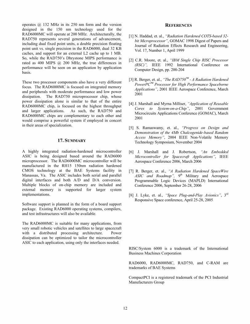
The RAD6000MC is an excellent match for use with the emerging Space Plug-and-Play Avionics for the SpaceWire (SPA-S) standard [8]. The Appliqué Sensor Interface Module (ASIM) requires both a SpaceWire interface and analog interfaces to sensors. The inclusion of both 1553 and PCI interfaces provides for connection to legacy peripherals as well as those that support the SpaceWire interface. A possible implementation of the RAD6000MC as the SPA-S ASIM is shown in Figure 11. In an ASIM application, information describing the capabilities of the sensors must be stored in non-volatile memory in XML-based transducer electronic datasheets (xTEDS) as part of the SPA standard. The RAD6000MC can support this requirement through either the use of the on-chip C-RAM non-volatile memory or by accessing external non-volatile memory.
Plug-and-play extensions to the SpaceWire standard are currently being refined that will affect the configuration port of the planned embedded router. The design team is tracking progress of this effort and will assess the ability to incorporate the most up-to-date changes into the SpaceWire router core prior to tape out of the microcontroller.
14. ADDITIONAL APPLICATIONS
The RAD6000MC is well suited for a wide variety of applications, ranging from use as the flight computer of a small satellite with moderate capabilities through use of multiple components in a very large distributed system such as a manned interplanetary spacecraft or orbiting space station. Instrument control and control of small planetary robotic vehicles are additional applications for which the RAD6000MC would be well suited, as evidenced by the current use of the RAD6000 microprocessor in the Spirit and Opportunity rovers.
In large distributed systems, the RAD6000MC ASIC would provide the ability to offload processing from the main spacecraft computer, and the flexible combination of interfaces would allow each RAD6000MC within the system to be optimized for power/performance for its specific functions. Inter-spacecraft communication would easily be supported via the SpaceWire router.
For robotic vehicle applications, the embedded analog interfaces provide options for sensor interface and tactile control feedback. This capability previously required additional components, located on another card. As such, a RAD6000MC-based implementation would reduce size and power dissipation as well as increase reliability through reduced interconnections.
For instrument control, the microcontroller can leverage its many interfaces to match the instrument to the preferred serial or parallel bus used by the satellite’s main computer. This capability may allow reuse of instrument platforms on multiple missions without any redesign of the hardware.
11
RAD6000MC
OSCRS422
28V(FLTR)
PC/SW
Test
Deb
ugS
PA
-S
RS422
Use
r Int
erfa
ce
RS422
clock
syncSpaceWire
+3.3+1.5
MemoryPCI
1553ADC, DACJTAG OutDiscretes
Serial Port
Test Bypass
JTAG In
SP
A-S
SP
A-S
SP
A-S
OSCASIM
ControlPOR
28V SwitchedUSER
PC User Voltages Switched
12Vor 5V
Figure 11: SPA-S ASIM based on RAD6000MC
15. POWER OPTIMIZATION FOR APPLICATIONS
Interfaces which are not required for a mission-specific application can be shut down by turning off their clocks to optimize power dissipation. This clock gating can be turned on or off via software commands, allowing interim shutdown when an interface is not in operation. Certain functions of the RAD6000MC are considered to be necessary for all applications, as they are essential to basic functionality. These include the RAD6000 microprocessor core itself and the LIF core, the EMC, the on-chip bus, the clock and test (CAT) core, and the miscellaneous (MISC) core. The JTAG master and slave test cores and the 16550-compatible UART are typically not in operation during an application unless a test procedure is in process. All of the other interface cores may be used in any combination for a specific application.
In addition, system clock speed may be adjusted for the application. The chip is being designed for both 33 MHz and 66 MHz operation. Other speeds may be employed as required, as the PCI interface will be supported by a separate oscillator to allow it to meet the PCI standard, the 1553 may be set up to meet the requirements, the PLL supporting the SpaceWire links is independent of the main clock speed in that programmable divide ratios can be adjusted to meet goals.
Power dissipation of the RAD6000MC is dependent upon both the system clock speed and the number of cores in operation. Early estimates are that in a relatively minimal configuration that is similar to that found in existing RAD6000 single board computers (RAD6000, memory, and PCI bus) with the processor operating @ 33 MHz, the
RAD6000MC will dissipate roughly 2 Watts. Running @ 66 MHz with all core functions in full operation, estimated power dissipation is approximately 6 Watts.
16. RAD6000MC PERFORMANCE
The rated performance of the original RAD6000 microprocessor was 35 Dhrystone MIPS @ 33 MHz. Of course, Dhrystone MIPS considers only fixed point instructions and an 8 KB cache, so the additional performance afforded by the floating point unit and the ability to execute both floating point and fixed point instructions simultaneously is neglected with this benchmark. The RAD6000MC plans to support 66 MHz, which would translate to approximately 70 Dhrystone MIPS when running at this speed. The RAD6000MC has not yet been calibrated using the SPECmark benchmark.
Most microcontroller components do not incorporate floating point hardware. However, for applications such as turning and pointing of an instrument using Kalman filtering algorithms, the advantage of the RAD6000MC’s floating point execution unit is significant. In a fixed point processor, several instructions may be required to manipulate the data to allow arithmetic operations such as multiplication without exceeding the range and incurring overflow. This translates to the need for a fixed point computer running at a much higher clock speed to maintain equivalent throughput, resulting in increased power dissipation and in higher susceptibility to single event transients.
Comparing the RAD6000MC to BAE Systems’ RAD750 microprocessor, the RAD750 currently in production
12
operates @ 132 MHz in its 250 nm form and the version designed in the 150 nm technology used for the RAD6000MC will operate at 200 MHz. Architecturally, the RAD750 represents several generations of advancement, including dual fixed point units, a double precision floating point unit vs. single precision in the RAD6000, dual 32 KB caches, and support for an external L2 cache up to 1 MB. So, while the RAD750’s Dhrystone MIPS performance is rated as 400 MIPS @ 200 MHz, the true differences in performance will be seen on an application by application basis.
These two processor components also have a very different focus. The RAD6000MC is focused on integrated memory and peripherals with moderate performance and low power dissipation. The RAD750 microprocessor chip, whose power dissipation alone is similar to that of the entire RAD6000MC chip, is focused on the highest throughput and larger applications. As such, the RAD750 and RAD6000MC chips are complementary to each other and would comprise a powerful system if employed in concert in their areas of specialization.
17. SUMMARY
A highly integrated radiation-hardened microcontroller ASIC is being designed based around the RAD6000 microprocessor. The RAD6000MC microcontroller will be manufactured in the RH15 150nm radiation hardened CMOS technology at the BAE Systems facility in Manassas, Va. The ASIC includes both serial and parallel digital interfaces and both A/D and D/A conversion. Multiple blocks of on-chip memory are included and external memory is supported for larger system implementations.
Software support is planned in the form of a board support package. Existing RAD6000 operating systems, compilers, and test infrastructures will also be available.
The RAD6000MC is suitable for many applications, from very small robotic vehicles and satellites to large spacecraft with a distributed processing architecture. Power dissipation can be optimized to tailor the microcontroller ASIC to each application, using only the interfaces needed.
REFERENCES
[1] N. Haddad, et. al., “Radiation Hardened COTS-based 32-bit Microprocessor”, GOMAC 1998 Digest of Papers and Journal of Radiation Effects Research and Engineering, Vol. 17, Number 1, April 1999
[2] C.R. Moore, et. al., “IBM Single Chip RISC Processor (RSC)”, IEEE 1992 International Conference on Computer Design, pp. 200-204
[3] R. Berger, et. al., “The RAD750TM - A Radiation Hardened PowerPCTM Processor for High Performance Spaceborne Applications”, 2001 IEEE Aerospace Conference, March 2001
[4] J. Marshall and Myrna Milliser, “Application of Reusable Cores to System-on-a-Chip”, 2001 Government Microcircuits Applications Conference (GOMAC), March 2001
[5] S. Ramaswamy, et. al., “Progress on Design and Demonstration of the 4Mb Chalcogenide-based Random Access Memory”, 2004 IEEE Non-Volatile Memory Technology Symposium, November 2004
[6] J. Marshall and J. Robertson, “An Embedded Microcontroller for Spacecraft Applications”, IEEE Aerospace Conference 2006, March 2006
[7] R. Berger, et. al., “A Radiation Hardened SpaceWire ASIC and Roadmap”, 9th Military and Aerospace Programmable Logic Devices (MAPLD) International Conference 2006, September 26-28, 2006
[8] J. Lyke, et. al., “Space Plug-and-Play Avionics”, 3rd Responsive Space conference, April 25-28, 2005
RISC/System 6000 is a trademark of the International Business Machines Corporation
RAD6000, RAD6000MC, RAD750, and C-RAM are trademarks of BAE Systems
CompactPCI is a registered trademark of the PCI Industrial Manufacturers Group

13
BIOGRAPHIES
Richard Berger is a senior principal systems engineer responsible for the development of advanced products and the insertion of state of the art technologies for aerospace applications. He has over twenty five years of circuit, logic, and system architecture design experience in high performance commercial and military semiconductors and processing systems at IBM, Loral, Lockheed Martin, and BAE Systems. Richard has recently been driving the development of complex mixed-signal and digital system-on-chip products. He has also provided management consulting services to a number of companies for the development of complex high technology products in a variety of industries. Richard has published numerous technical papers related to spaceborne processors and radiation effects. Richard received a BSEE degree from Rutgers University in 1978.
Myrna Milliser is a Senior Principal Electrical Engineer in ASIC design and development at BAE Systems in Manassas, Virginia. She has over 20 years experience in ASIC design and design management across several generations of CMOS technologies at IBM, Lockheed Martin and BAE Systems. She was team lead for the reusable cores developed for the Power PCI bridge ASIC for the JPL X2000 program and the ASIC design manager for subsequent core based ASICs: Enhanced Power PCI bridge, SpaceWire ASIC, and Golden Gate Power PCI bridge. Myrna has a BS and a MS in mathematics from James Madison University and a BSEE from the University of Virginia.
Dan Stanley is a senior principal engineer at BAE Sytems in Manassas, Virginia. He has over twenty years of experience as an ASIC designer. He has been the lead designer for numerous radiation hardened ASICs for spacebourne applications. Dan received a BSEE degree from Virginia Polytechnic Institute and State University in 1985.
David Hutcheson is a senior principal electrical engineer responsible for development and verification of digital electronics for space applications. Since joining BAE Systems (then IBM Federal Systems) in 1982, Mr. Hutcheson has participated in the design, production, and test of a variety of data processing and interface systems for use in commercial, Navy, Air Force, and space systems. His
current focus is spread across a broad spectrum of single-board computers, FPGAs, and ASIC designs. David received a BS degree in Electrical Engineering from the University of Virginia.
Jennifer Koehler is a principal electrical engineer that has worked for BAE Systems for over 10 years. Her focus is VHDL, and has created many key designs for ASICs and FPGAs. In the past, she has worked closely with Northrop Grumman on their AEHF program, and also worked with NASA Goddard to incorporate the SpaceWire interface into BAE Systems’ SpaceWire ASIC. Ree has been leading up the full-chip verification of several ASICs, as well as formal verification of these designs. On the side, she is one of the leaders for the company’s Women In Technology program for local high school female students. Jennifer graduated with a BSEE from the University of Virginia in 1996.
Dave Moser is a senior principal ASIC engineer responsible for the development of ASIC and custom chip for aerospace and general military applications. He has over fifteen years of logic (FPGA and ASIC), software and system architecture design experience in commercial and military semiconductors and processing systems at ManTech, Loral, Lockheed Martin, Real3D and BAE Systems. Dave has recently completed a low power DSP style ASIC design in which the original power budget was reduced by 75%. He has also led the verification of the RAD750 and is currently designing a low power solution for a night vision goggle. Dave has led the design effort on 10+ FPGAs and 4 ASIC designs.
Laura Burcin is a senior program manager at BAE Systems in Manassas, VA. Ms. Burcin has over twenty-three years of technical and management experience in space technology development. She is presently the Program Manager for technology programs including the Rad Hard GFLOPS Processor, Universal FPGA Support Device and RAD6000MC microcontroller development programs. Prior program management experience includes the Chalcogenide Random Access Memory, RAD750 and DARPA Power Aware Computing and Communications development programs. Ms. Burcin spent four years in engineering management at both the department and project level. Prior to technical management Ms. Burcin was a system engineer for numerous missile and space processor programs. She received her B.S. in Biology from the University of Kentucky in 1981 and her M.S. in Computer Science from the University of Louisville in 1983.

14
Randy Zeger is a senior principal engineer involved with ASIC and board level design for the space industry. He has over eighteen years of circuit, logic, and analog design experience with concentrations on signal integrity and mitigation of EMI and radiation effects. Randy has recently been a hardware lead responsible for developing boards for a high-speed satellite communications system. Randy received a BSEET degree from DeVry University in 1989.
Benjamin J. Blalock received his B.S. degree in electrical engineering from The University of Tennessee, Knoxville, in 1991 and the M.S. and Ph.D. degrees, also in electrical engineering, from the Georgia Institute of Technology, Atlanta, in 1993 and 1996 respectively. He is currently an Associate Professor in the Department of Electrical Engineering and Computer Science at The University of Tennessee where he directs the Integrated Circuits and Systems Laboratory (ICASL). His research focus there includes analog integrated circuit design for extreme environments (both wide temperature and radiation) on CMOS and SiGe BiCMOS, multi-gate transistors and circuits on SOI, analog circuit techniques for sub 100-nm CMOS, mixed-signal/mixed-voltage circuit design for systems-on-a-chip, and biomicroelectronics. Dr. Blalock has co-authored over 80 refereed papers. He has also worked as an analog IC design consultant. Dr. Blalock is a senior member of the IEEE.
Mark Hale was born in Kingsport, TN in 1980. He is currently a Ph.D. candidate in the Integrated Circuits and Systems Laboratory at the University of Tennessee, Knoxville. He received the B.S. and M.S. degrees from the University of Tennessee in 2002 and 2004, respectively. His research interest is in the design of D/A and A/D converters. He is joining Cadence Design Systems, Cary, NC in January 2008.