The MOSFET Citation 12 The Audio Amateur, 2/81 - First Watt
14
The MOSFET Citation 12 The Audio Amateur, 2/81 Copyright Nelson Pass Audio Amateur has published a number of projects modifying popular kits, usually Dynaco's. Obviously it is much less expensive to use the chassis and power supply, pots, connectors, switches, PC boards, and heat sinks that can be had for the price of a kit than to buy the components individually or have them made. Creating a one-off copy commercially typically costs as much as making 10 copies of the same item, because the dominant costs are design and set-up time which do not increase with quantity. Small wonder then that most technicians and designers who write for this and similar magazines base their projects on yesterday's readily available kits, which, often as not, languish unappreciated in closets and basements. This is one such project. We will, however, do two things here you may not have seen before. We'll modify the Harmon Kardon Citation 12, a popular device which has somehow escaped the kit modifier's attention; and we'll do so with power mosfet circuitry instead of the traditional bipolar power transistors. This project is for experienced builders only, and Harmon Kardon want me to remind you that it will void any warranty coverage on the Citation 12. THE HARMON KARDON CITATION 12 The Citation 12, introduced about 10 years ago, is based on the circuitry found in the RCA transistor manuals (for example, see RCA data sheet file #647). This circuitry was the basis for nearly all the quasi-complementary designs in existence, as typified by the large power amplifiers of the early '70's. In its time the Citation 12 was a truly excellent amplifier, employing a number of concepts which have only recently become popular: dual split power supplies, DC output coupling, and no active current limiting. These characteristics allowed it to sonically outperform the Dynaco 120 which was its popular competitor. It could drive anything with high reliability, and in the time I spent as a repair technician I fixed a few Dynaco, Phase Linear, McIntosh, Pioneer, and Sansui amplifiers, but I've never seen a broken Citation 12. I have another, nostalgic, reason for choosing the Citation 12: it was the first amplifier I built myself. About eight years ago, when I was an impecunious student working part- time for ESS Inc. (no, I did not design their electronics), the home-brew power amplifier built by a friend broke down, leaving me without music. Like most of you in a similar position, I decided to do without some other necessity, and shortly my kitchen table was covered with solder blobs and the parts to the Citation 12. I decided to fire up the completed unit on a variac instead of merely plugging it into the wall' and was dismayed to discover that both channels exhibited extremely large DC offset when I applied AC power. After some weeks of rechecking my work and finding
Transcript of The MOSFET Citation 12 The Audio Amateur, 2/81 - First Watt

The MOSFET Citation 12The Audio Amateur, 2/81Copyright Nelson Pass
Audio Amateur has published a number of projects modifying popular kits, usuallyDynaco's. Obviously it is much less expensive to use the chassis and power supply, pots,connectors, switches, PC boards, and heat sinks that can be had for the price of a kit thanto buy the components individually or have them made. Creating a one-off copycommercially typically costs as much as making 10 copies of the same item, because thedominant costs are design and set-up time which do not increase with quantity. Smallwonder then that most technicians and designers who write for this and similar magazinesbase their projects on yesterday's readily available kits, which, often as not, languishunappreciated in closets and basements. This is one such project.
We will, however, do two things here you may not have seen before. We'll modify theHarmon Kardon Citation 12, a popular device which has somehow escaped the kitmodifier's attention; and we'll do so with power mosfet circuitry instead of the traditionalbipolar power transistors. This project is for experienced builders only, and HarmonKardon want me to remind you that it will void any warranty coverage on the Citation 12.
THE HARMON KARDON CITATION 12
The Citation 12, introduced about 10 years ago, is based on the circuitry found in theRCA transistor manuals (for example, see RCA data sheet file #647). This circuitry wasthe basis for nearly all the quasi-complementary designs in existence, as typified by thelarge power amplifiers of the early '70's.
In its time the Citation 12 was a truly excellent amplifier, employing a number ofconcepts which have only recently become popular: dual split power supplies, DC outputcoupling, and no active current limiting. These characteristics allowed it to sonicallyoutperform the Dynaco 120 which was its popular competitor. It could drive anythingwith high reliability, and in the time I spent as a repair technician I fixed a few Dynaco,Phase Linear, McIntosh, Pioneer, and Sansui amplifiers, but I've never seen a brokenCitation 12.
I have another, nostalgic, reason for choosing the Citation 12: it was the first amplifier Ibuilt myself. About eight years ago, when I was an impecunious student working part-time for ESS Inc. (no, I did not design their electronics), the home-brew power amplifierbuilt by a friend broke down, leaving me without music. Like most of you in a similarposition, I decided to do without some other necessity, and shortly my kitchen table wascovered with solder blobs and the parts to the Citation 12.
I decided to fire up the completed unit on a variac instead of merely plugging it into thewall' and was dismayed to discover that both channels exhibited extremely large DCoffset when I applied AC power. After some weeks of rechecking my work and finding
no errors, I finally decided to connect it up and plug it into the wall anyway*. When I did,the woofers on my speakers plunged fully forward as if attempting to escape theamplifier, but after a few seconds they returned to normal and music appeared. Thus Idiscovered one of the Citation's few faults: an enormous subsonic turn-on thump.
I kept the amplifier for several years and ultimately sold it to a friend, only to end upbuying it back. It sat in my closet for a long time, a candidate for that perfect project,until one day at Threshold we discovered a vendor had accidentally shipped us severalpower mosfets instead of diodes, and this article began falling into place. The powermosfets, reasonable analogs of the hometaxial npn devices in the Citation 12, fit quiteneatly into the original layout and provide for a state-of-the-art super-position upon aclassic piece of circuitry, improving the speed and distortion characteristics in an evenmore simple topology than in the original.
POWER MOSFETS
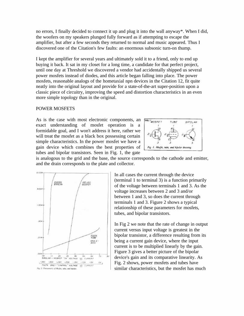
As is the case with most electronic components, anexact understanding of mosfet operation is aformidable goal, and I won't address it here, rather wewill treat the mosfet as a black box possessing certainsimple characteristics. In the power mosfet we have again device which combines the best properties oftubes and bipolar transistors. Seen in Fig. 1, the gateis analogous to the grid and the base, the source corresponds to the cathode and emitter,and the drain corresponds to the plate and collector.
In all cases the current through the device(terminal 1 to terminal 3) is a function primarilyof the voltage between terminals 1 and 3. As thevoltage increases between 2 and 3 and/orbetween 1 and 3, so does the current throughterminals 1 and 3. Figure 2 shows a typicalrelationship of these parameters for mosfets,tubes, and bipolar transistors.
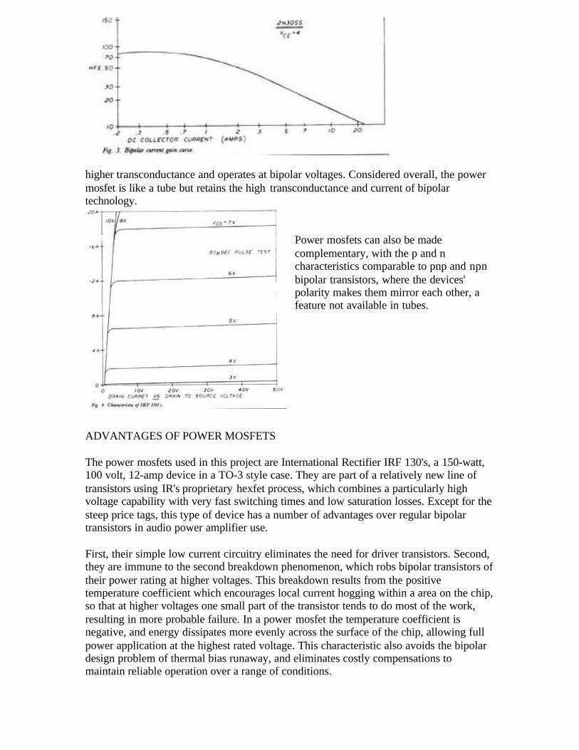
In Fig 2 we note that the rate of change in outputcurrent versus input voltage is greatest in thebipolar transistor, a difference resulting from itsbeing a current gain device, where the inputcurrent is to be multiplied linearly by the gain.Figure 3 gives a better picture of the bipolardevice's gain and its comparative linearity. AsFig. 2 shows, power mosfets and tubes havesimilar characteristics, but the mosfet has much
higher transconductance and operates at bipolar voltages. Considered overall, the powermosfet is like a tube but retains the high transconductance and current of bipolartechnology.
Power mosfets can also be madecomplementary, with the p and ncharacteristics comparable to pnp and npnbipolar transistors, where the devices'polarity makes them mirror each other, afeature not available in tubes.
ADVANTAGES OF POWER MOSFETS
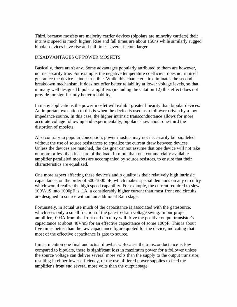
The power mosfets used in this project are International Rectifier IRF 130's, a 150-watt,100 volt, 12-amp device in a TO-3 style case. They are part of a relatively new line oftransistors using IR's proprietary hexfet process, which combines a particularly highvoltage capability with very fast switching times and low saturation losses. Except for thesteep price tags, this type of device has a number of advantages over regular bipolartransistors in audio power amplifier use.
First, their simple low current circuitry eliminates the need for driver transistors. Second,they are immune to the second breakdown phenomenon, which robs bipolar transistors oftheir power rating at higher voltages. This breakdown results from the positivetemperature coefficient which encourages local current hogging within a area on the chip,so that at higher voltages one small part of the transistor tends to do most of the work,resulting in more probable failure. In a power mosfet the temperature coefficient isnegative, and energy dissipates more evenly across the surface of the chip, allowing fullpower application at the highest rated voltage. This characteristic also avoids the bipolardesign problem of thermal bias runaway, and eliminates costly compensations tomaintain reliable operation over a range of conditions.
Third, because mosfets are majority carrier devices (bipolars are minority carriers) theirintrinsic speed is much higher. Rise and fall times are about 150ns while similarly ruggedbipolar devices have rise and fall times several factors larger.
DISADVANTAGES OF POWER MOSFETS
Basically, there aren't any. Some advantages popularly attributed to them are however,not necessarily true. For example, the negative temperature coefficient does not in itselfguarantee the device is indestructible. While this characteristic eliminates the secondbreakdown mechanism, it does not offer better reliability at lower voltage levels, so thatin many well designed bipolar amplifiers (including the Citation 12) this effect does notprovide for significantly better reliability.
In many applications the power mosfet will exhibit greater linearity than bipolar devices.An important exception to this is when the device is used as a follower driven by a lowimpedance source. In this case, the higher intrinsic transconductance allows for moreaccurate voltage following and experimentally, bipolars show about one-third thedistortion of mosfets.
Also contrary to popular conception, power mosfets may not necessarily be paralleledwithout the use of source resistances to equalize the current draw between devices.Unless the devices are matched, the designer cannot assume that one device will not takeon more or less than its share of the load. In more than one commercially availableamplifier paralleled mosfets are accompanied by source resistors, to ensure that theircharacteristics are equalized.
One more aspect affecting these device's audio quality is their relatively high intrinsiccapacitance, on the order of 500-1000 pF, which makes special demands on any circuitrywhich would realize the high speed capability. For example, the current required to slew100V/uS into 1000pF is .1A, a considerably higher current than most front end circuitsare designed to source without an additional Rain stage.
Fortunately, in actual use much of the capacitance is associated with the gatesource,which sees only a small fraction of the gate-to-drain voltage swing. In our projectamplifier, .003A from the front end circuitry will drive the positive output transistor'scapacitance at about 40V/uS for an effective capacitance of some 100pF. This is aboutfive times better than the raw capacitance figure quoted for the device, indicating thatmost of the effective capacitance is gate to source.
I must mention one final and actual drawback. Because the transconductance is lowcompared to bipolars, there is significant loss in maximum power for a follower unlessthe source voltage can deliver several more volts than the supply to the output transistor,resulting in either lower efficiency, or the use of tiered power supplies to feed theamplifier's front end several more volts than the output stage.
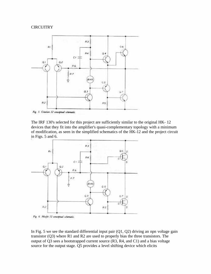
CIRCUITRY
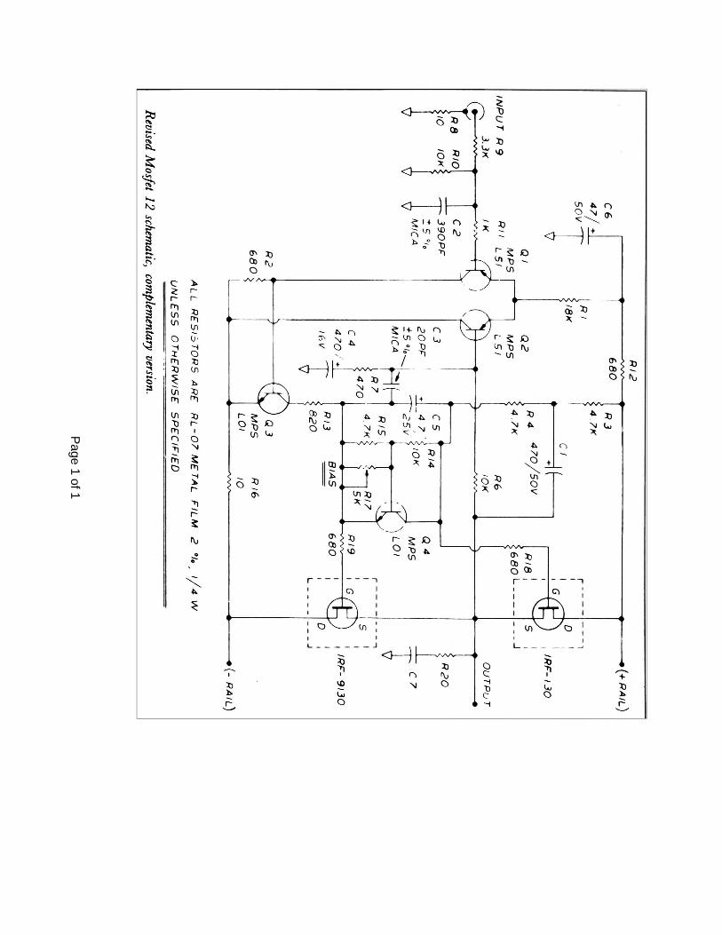
The IRF 130's selected for this project are sufficiently similar to the original HK- 12devices that they fit into the amplifier's quasi-complementary topology with a minimumof modification, as seen in the simplified schematics of the HK-12 and the project circuitin Figs. 5 and 6.
In Fig. 5 we see the standard differential input pair (Q1, Q2) driving an npn voltage gaintransistor (Q3) where R1 and R2 are used to properly bias the three transistors. Theoutput of Q3 sees a bootstrapped current source (R3, R4, and C1) and a bias voltagesource for the output stage. Q5 provides a level shifting device which elicits
complementary action from Q7, the negative output transistor, and Q4 provides thefollower current gain to drive Q6, the positive output transistor. The Fig. 6 circuit isbasically the same; but Q6 and Q7 have become power mosfets and Q4 has disappearedbecause the additional current gain is not required to drive Q6.
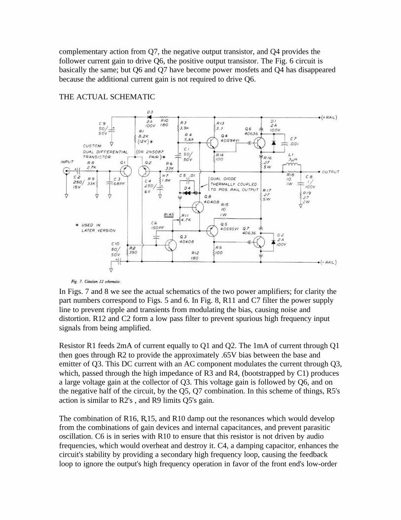
THE ACTUAL SCHEMATIC
In Figs. 7 and 8 we see the actual schematics of the two power amplifiers; for clarity thepart numbers correspond to Figs. 5 and 6. In Fig. 8, R11 and C7 filter the power supplyline to prevent ripple and transients from modulating the bias, causing noise anddistortion. R12 and C2 form a low pass filter to prevent spurious high frequency inputsignals from being amplified.
Resistor R1 feeds 2mA of current equally to Q1 and Q2. The 1mA of current through Q1then goes through R2 to provide the approximately .65V bias between the base andemitter of Q3. This DC current with an AC component modulates the current through Q3,which, passed through the high impedance of R3 and R4, (bootstrapped by C1) producesa large voltage gain at the collector of Q3. This voltage gain is followed by Q6, and onthe negative half of the circuit, by the Q5, Q7 combination. In this scheme of things, R5'saction is similar to R2's , and R9 limits Q5's gain.
The combination of R16, R,15, and R10 damp out the resonances which would developfrom the combinations of gain devices and internal capacitances, and prevent parasiticoscillation. C6 is in series with R10 to ensure that this resistor is not driven by audiofrequencies, which would overheat and destroy it. C4, a damping capacitor, enhances thecircuit's stability by providing a secondary high frequency loop, causing the feedbackloop to ignore the output's high frequency operation in favor of the front end's low-order
output at frequencies above 800kHz. This allows the amplifier's input stage to dominatethe high frequency response with a less than two-pole characteristic, providing for highstability under transient conditions.
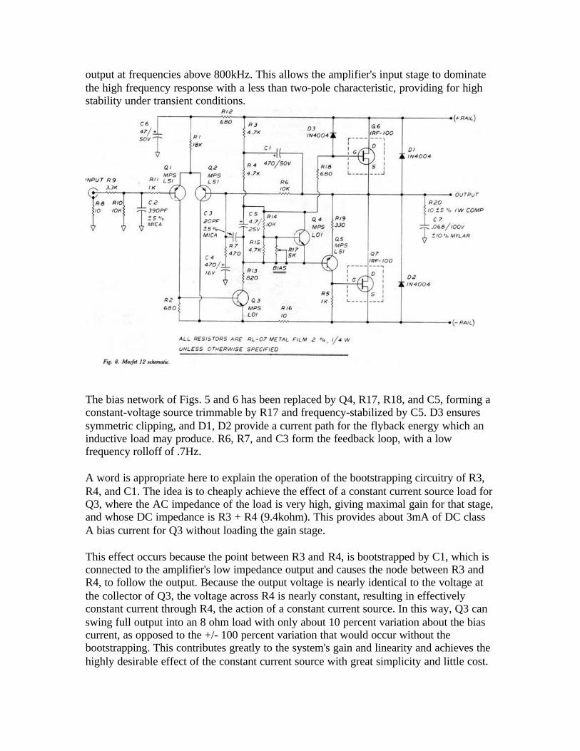
The bias network of Figs. 5 and 6 has been replaced by Q4, R17, R18, and C5, forming aconstant-voltage source trimmable by R17 and frequency-stabilized by C5. D3 ensuressymmetric clipping, and D1, D2 provide a current path for the flyback energy which aninductive load may produce. R6, R7, and C3 form the feedback loop, with a lowfrequency rolloff of .7Hz.
A word is appropriate here to explain the operation of the bootstrapping circuitry of R3,R4, and C1. The idea is to cheaply achieve the effect of a constant current source load forQ3, where the AC impedance of the load is very high, giving maximal gain for that stage,and whose DC impedance is R3 + R4 (9.4kohm). This provides about 3mA of DC classA bias current for Q3 without loading the gain stage.
This effect occurs because the point between R3 and R4, is bootstrapped by C1, which isconnected to the amplifier's low impedance output and causes the node between R3 andR4, to follow the output. Because the output voltage is nearly identical to the voltage atthe collector of Q3, the voltage across R4 is nearly constant, resulting in effectivelyconstant current through R4, the action of a constant current source. In this way, Q3 canswing full output into an 8 ohm load with only about 10 percent variation about the biascurrent, as opposed to the +/- 100 percent variation that would occur without thebootstrapping. This contributes greatly to the system's gain and linearity and achieves thehighly desirable effect of the constant current source with great simplicity and little cost.
The effect is good across the AC band, rolling off at about .14Hz on the low end and atabout 300kHz at high frequencies.
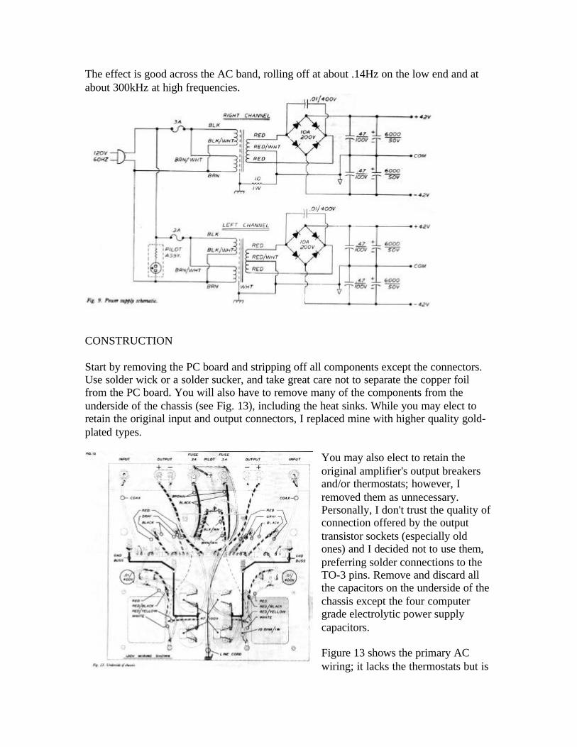
CONSTRUCTION
Start by removing the PC board and stripping off all components except the connectors.Use solder wick or a solder sucker, and take great care not to separate the copper foilfrom the PC board. You will also have to remove many of the components from theunderside of the chassis (see Fig. 13), including the heat sinks. While you may elect toretain the original input and output connectors, I replaced mine with higher quality gold-plated types.
You may also elect to retain theoriginal amplifier's output breakersand/or thermostats; however, Iremoved them as unnecessary.Personally, I don't trust the quality ofconnection offered by the outputtransistor sockets (especially oldones) and I decided not to use them,preferring solder connections to theTO-3 pins. Remove and discard allthe capacitors on the underside of thechassis except the four computergrade electrolytic power supplycapacitors.
Figure 13 shows the primary ACwiring; it lacks the thermostats but is
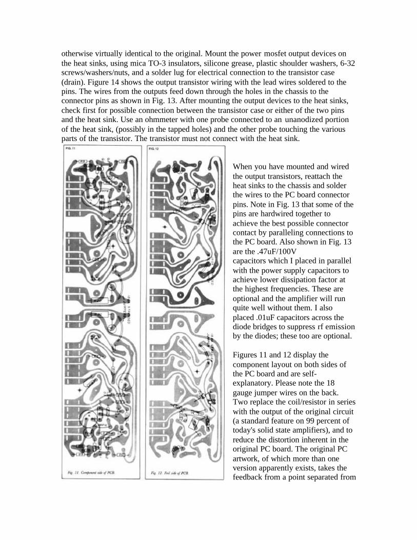
otherwise virtually identical to the original. Mount the power mosfet output devices onthe heat sinks, using mica TO-3 insulators, silicone grease, plastic shoulder washers, 6-32screws/washers/nuts, and a solder lug for electrical connection to the transistor case(drain). Figure 14 shows the output transistor wiring with the lead wires soldered to thepins. The wires from the outputs feed down through the holes in the chassis to theconnector pins as shown in Fig. 13. After mounting the output devices to the heat sinks,check first for possible connection between the transistor case or either of the two pinsand the heat sink. Use an ohmmeter with one probe connected to an unanodized portionof the heat sink, (possibly in the tapped holes) and the other probe touching the variousparts of the transistor. The transistor must not connect with the heat sink.
When you have mounted and wiredthe output transistors, reattach theheat sinks to the chassis and solderthe wires to the PC board connectorpins. Note in Fig. 13 that some of thepins are hardwired together toachieve the best possible connectorcontact by paralleling connections tothe PC board. Also shown in Fig. 13are the .47uF/100Vcapacitors which I placed in parallelwith the power supply capacitors toachieve lower dissipation factor atthe highest frequencies. These areoptional and the amplifier will runquite well without them. I alsoplaced .01uF capacitors across thediode bridges to suppress rf emissionby the diodes; these too are optional.
Figures 11 and 12 display thecomponent layout on both sides ofthe PC board and are self-explanatory. Please note the 18gauge jumper wires on the back.Two replace the coil/resistor in serieswith the output of the original circuit(a standard feature on 99 percent oftoday's solid state amplifiers), and toreduce the distortion inherent in theoriginal PC board. The original PCartwork, of which more than oneversion apparently exists, takes thefeedback from a point separated from
the actual output node by a short length of copper which carries an asymmetrical portionof the output current. The feedback thus operates off a voltage several milivolts removedfrom the actual output generating even-ordered distortions.
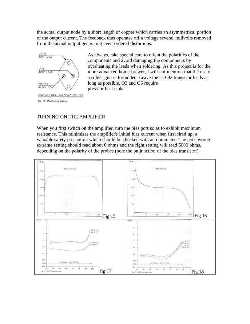
As always, take special care to orient the polarities of thecomponents and avoid damaging the components byoverheating the leads when soldering. As this project is for themore advanced home-brewer, I will not mention that the use ofa solder gun is forbidden. Leave the TO-92 transistor leads aslong as possible. Q3 and Q5 requirepress-fit heat sinks.
TURNING ON THE AMPLIFIER
When you first switch on the amplifier, turn the bias pots so as to exhibit maximumresistance. This minimizes the amplifier's initial bias current when first fired up, avaluable safety precaution which should be checked with an ohmmeter. The pot's wrongextreme setting should read about 0 ohms and the right setting will read 5000 ohms,depending on the polarity of the probes (note the pn junction of the bias transistor).
Fig 15 Fig 16
fig 17 Fig 18
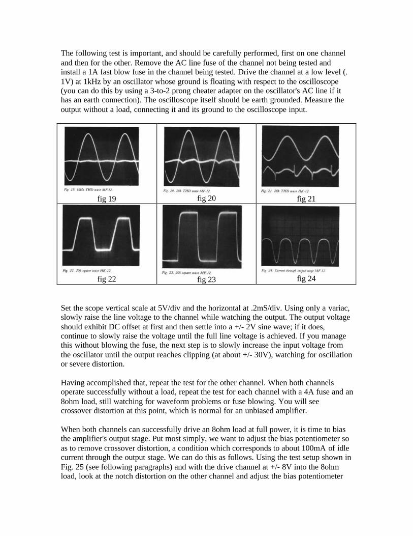
The following test is important, and should be carefully performed, first on one channeland then for the other. Remove the AC line fuse of the channel not being tested andinstall a 1A fast blow fuse in the channel being tested. Drive the channel at a low level (.1V) at 1kHz by an oscillator whose ground is floating with respect to the oscilloscope(you can do this by using a 3-to-2 prong cheater adapter on the oscillator's AC line if ithas an earth connection). The oscilloscope itself should be earth grounded. Measure theoutput without a load, connecting it and its ground to the oscilloscope input.
fig 19 fig 20 fig 21
fig 22 fig 23 fig 24
Set the scope vertical scale at 5V/div and the horizontal at .2mS/div. Using only a variac,slowly raise the line voltage to the channel while watching the output. The output voltageshould exhibit DC offset at first and then settle into a +/- 2V sine wave; if it does,continue to slowly raise the voltage until the full line voltage is achieved. If you managethis without blowing the fuse, the next step is to slowly increase the input voltage fromthe oscillator until the output reaches clipping (at about +/- 30V), watching for oscillationor severe distortion.
Having accomplished that, repeat the test for the other channel. When both channelsoperate successfully without a load, repeat the test for each channel with a 4A fuse and an8ohm load, still watching for waveform problems or fuse blowing. You will seecrossover distortion at this point, which is normal for an unbiased amplifier.
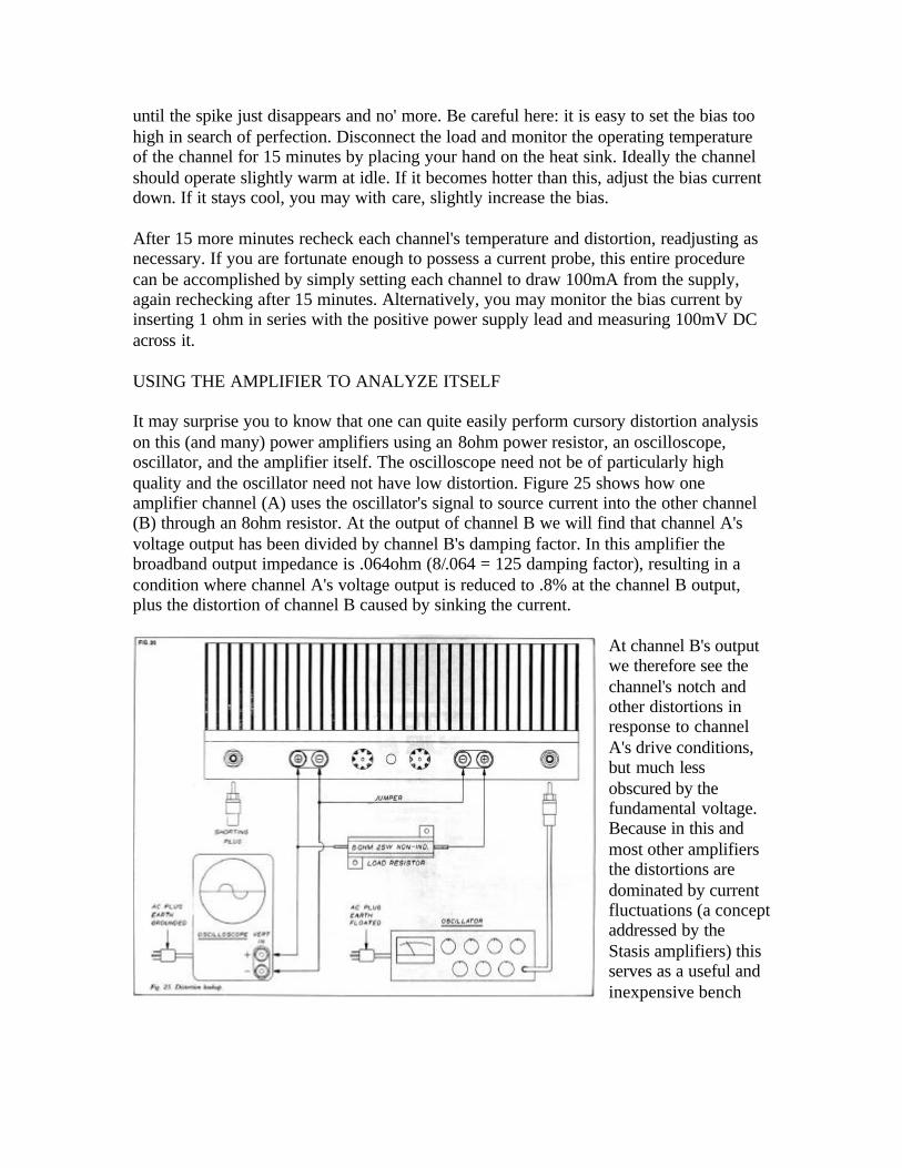
When both channels can successfully drive an 8ohm load at full power, it is time to biasthe amplifier's output stage. Put most simply, we want to adjust the bias potentiometer soas to remove crossover distortion, a condition which corresponds to about 100mA of idlecurrent through the output stage. We can do this as follows. Using the test setup shown inFig. 25 (see following paragraphs) and with the drive channel at +/- 8V into the 8ohmload, look at the notch distortion on the other channel and adjust the bias potentiometer
until the spike just disappears and no' more. Be careful here: it is easy to set the bias toohigh in search of perfection. Disconnect the load and monitor the operating temperatureof the channel for 15 minutes by placing your hand on the heat sink. Ideally the channelshould operate slightly warm at idle. If it becomes hotter than this, adjust the bias currentdown. If it stays cool, you may with care, slightly increase the bias.
After 15 more minutes recheck each channel's temperature and distortion, readjusting asnecessary. If you are fortunate enough to possess a current probe, this entire procedurecan be accomplished by simply setting each channel to draw 100mA from the supply,again rechecking after 15 minutes. Alternatively, you may monitor the bias current byinserting 1 ohm in series with the positive power supply lead and measuring 100mV DCacross it.
USING THE AMPLIFIER TO ANALYZE ITSELF
It may surprise you to know that one can quite easily perform cursory distortion analysison this (and many) power amplifiers using an 8ohm power resistor, an oscilloscope,oscillator, and the amplifier itself. The oscilloscope need not be of particularly highquality and the oscillator need not have low distortion. Figure 25 shows how oneamplifier channel (A) uses the oscillator's signal to source current into the other channel(B) through an 8ohm resistor. At the output of channel B we will find that channel A'svoltage output has been divided by channel B's damping factor. In this amplifier thebroadband output impedance is .064ohm (8/.064 = 125 damping factor), resulting in acondition where channel A's voltage output is reduced to .8% at the channel B output,plus the distortion of channel B caused by sinking the current.
At channel B's outputwe therefore see thechannel's notch andother distortions inresponse to channelA's drive conditions,but much lessobscured by thefundamental voltage.Because in this andmost other amplifiersthe distortions aredominated by currentfluctuations (a conceptaddressed by theStasis amplifiers) thisserves as a useful andinexpensive bench
technique and for the most part it is easy to see the distortion added to a .8%fundamental. This procedure is useful in biasing the amplifier as you can clearly seecrossover notch and other effects.
This test will also reveal distortions caused by poor connections between the PC boardand the connectors (something I encountered in the actual unit and which I cured bycleaning and reseating the connectors). To evaluate the percentage of distortionremember that the voltages seen by the 'scope divided by the output voltage of the otherchannel will equal the fraction of distortion. For example, if channel A's output is at +/-28V (20VRMS) through the 8 Ohms into channel B, then channel B's output will show asignal comprised of channel A's fundamental divided by the damping factor (for +/-.225V sinewave) plus an equivalent of channel B's distortion when operated at that levelinto 8ohm. In this case a .28V peak distortion spike would indicate a 1% peak distortion(not uncommon in amplifier's with . 1% average distortion).
PERFORMANCE
Figures 15-24 document the performance of the prototype amplifier, which was builtwithout selected components. Of particular note are the distortion and square wavecomparisons against the original, showing a significant improvement in distortioncharacteristic and transient response. Figure 24 shows the current waveform through halfthe output stage. Note that the current through the output device idles down instead ofshutting off abruptly as in bipolar Class B and AB amplifiers. This gives reducedcrossover distortion and the quasi-Class A operation at lower levels which otherwise wecould only achieve in a bipolar circuit with dynamic biasing.
The amplifier is sonically a significant improvement over the original, particularly in thehigh end where the Citation 12's veiled characteristic is replaced by a detailed, somewhatsweet sound. The imaging and midrange definition are also much improved; but the bassresponse (one of the Citation 1 2's strongest points) remains much the same ideal forplanar loudspeakers like MG II's, less so for acoustic suspension woofers.
In conclusion, I hope many of you will try this one and enjoy yourselves. No amplifiersounds as good as the one you built yourself*, and certainly no commercial amplifier willgive you as much satisfaction or frustration. As careful as the Editor and I have been,there is probably an error or two; I recommend that you cross-check the parts list,schematic, and pc board layout.
My amplifier has performed well for six months, as of this writing, and I encountered noexotic problems during its construction and testing.
Good luck. and have fun. n
Page 1 of 1


![Amateur Operato Advanced - Australian Maritime College · Amateur Operato Advanced Syllabus and Examination. The Amateur Licence (amateur advanced station) [the Advanced Amateur Licence]](https://static.fdocuments.net/doc/165x107/5f072ed67e708231d41bb822/amateur-operato-advanced-australian-maritime-college-amateur-operato-advanced.jpg)