The Morphology and Topography of Polymer Surfaces and ...epubs.surrey.ac.uk/738089/2/The Morphology...
31
- 1 - The Morphology and Topography of Polymer Surfaces and Interfaces Exposed by Ultra-Low-Angle Microtomy. Steven J. Hinder 1* , Chris Lowe 2 , James T. Maxted 2 , John F. Watts 1 . 1 The Surface Analysis Laboratory, School of Engineering, University of Surrey, Guildford, Surrey GU2 7XH, UK. 2 Becker Industrial Coatings Ltd, Goodlass Road, Speke, Liverpool L24 9HJ, UK.
Transcript of The Morphology and Topography of Polymer Surfaces and ...epubs.surrey.ac.uk/738089/2/The Morphology...

- 1 -
The Morphology and Topography of Polymer Surfaces and Interfaces Exposed by Ultra-Low-Angle Microtomy.
Steven J. Hinder1*
, Chris Lowe2, James T. Maxted
2, John F. Watts
1.
1The Surface Analysis Laboratory, School of Engineering, University of Surrey,
Guildford, Surrey GU2 7XH, UK.
2Becker Industrial Coatings Ltd, Goodlass Road, Speke, Liverpool L24 9HJ, UK.

- 2 -
Abstract :
The ultra-low-angle microtomy (ULAM) technique has been developed to impart a
cross-sectional, ultra-low-angle taper through polymeric materials such as coatings
and paints. ULAM employs a conventional rotary microtome in combination with
high-precision, angled sectioning blocks to fabricate the ultra-low-angle tapers.
Subsequent investigation of the tapers produced by ULAM may be used in
conjunction with X-ray photoelectron spectroscopy (XPS) or time-of-flight secondary
ion mass spectrometry (ToF-SIMS), for compositional depth profiling or ‘buried’
interface analysis. Variation in the selection of the ULAM taper angle and/or the
analysis interval size employed enables depth resolution at the nanometre or
micrometre scales to be achieved.
In the work described here scanning electron microscopy (SEM) and atomic force
microscopy (AFM) have been employed to investigate the morphology and
topography of the surfaces resulting from the ULAM tapering process. It is
demonstrated that a correctly mounted polymeric sample, sectioned with a sharp
microtome knife, displays little perturbation of the resulting polymeric surface after
ULAM processing. Additionally, SEM analysis of the interface region between a
poly(vinylidene fluoride) (PVdF) topcoat and polyurethane (PU) primer exposed by
ULAM processing reveals that the interface region between the two coatings
possesses a well-defined boundary. No evidence of polymeric smearing across the
interface is observed. XPS compositional depth profiling across a ‘buried’ PVdF/PU

- 3 -
interface, exposed by ULAM processing, is employed to demonstrate the utility of the
ULAM technique.
Keywords :
Ultra-low-angle microtomy; Polymeric coatings; Depth profiling; Multilayer
interfaces; Scanning electron microscopy; Atomic force microscopy; X-ray
photoelectron spectroscopy.
Running Headline : Morphology and Topography of Polymer Surfaces and Interfaces by ULAM.

- 4 -
1. Introduction. The desire to probe below the surface of a sample either to investigate changes of
composition with depth or to access interfaces ‘buried’ below overlying material is a
common challenge encountered by the materials scientist or engineer. Surface
specific depth profiling techniques such as angle resolved X-ray photoelectron
spectroscopy can be employed to produce composition depth profiles but are usually
limited to the topmost 5nm or so of the sample material [1]. Alternatively techniques
such as Rutherford backscattering spectroscopy can probe sample depths approaching
1µm [2]. However, whilst sputter depth profiling using noble gas or liquid metal ions
is the most widely employed technique to produce compositional depth profiles the
technique is typically limited to a few microns in materials which sputter in a
predictable and non-degrading manner. Polymers are not amenable to this means of
processing. If it is necessary to probe deep below the surface and yet retain depth
resolution, alternative methods must be sought.
A different approach to the direct analysis techniques described above is to employ an
instrument such as a microtome to produce cross-sections through a material by
means of a series of serial sections for subsequent analysis. Girois et al have
employed microtomed sections 40µm thick to investigate the photooxidation of
isotactic polypropylene [3] whilst Anton-Prinet et al used 20µm thick serial sections
to produce degradation thickness profiles of poly(vinyl chloride) that had undergone
photoageing [4]. Although the microtoming technique has been applied to a wide
range of polymeric materials, the depth resolution achievable is governed by the

- 5 -
practicalities of cutting and handling the material sections produced, typically a
resolution of no better than 6-10µm can be achieved when sectioning polymeric
samples [5].
The use of ex-situ mechanical techniques that remove material from a sample in a
precise manner and that produce specimens possessing a well-defined geometry have
a well documented history. Two such techniques that have been widely reported are
those of ball cratering and angle lapping. In the ball cratering procedure a steel ball
bearing coated in a diamond paste is rotated against a specimen so as to produce a
shallow crater at the sample surface. The specimen must then be introduced to a
spectrometer and a brief ion etch of the tapered surface employed to remove any
contaminants from the ball cratering procedure. Linescan or point analysis by Auger
electron spectroscopy along the crater wall then yields a compositional depth profile
of the sample material [6,7]. The angle lapping technique [8] was the forerunner of
ball cratering, in that sample material is removed from a specimen by abrading and
polishing. In the angle lapping procedure the specimen is polished at an angle of <3°
so as to produce a shallow taper through the material of interest. As with ball
cratering the lapped specimen must be introduced to a spectrometer and a brief ion
etch of the tapered surface performed to remove any contaminants from the angle
lapping process. A linescan or point analysis along the tapered surface of the sample
yields a compositional depth profile that can be readily converted to a depth of
analysis from the starting point.
- 6 -
Ball cratering and angle lapping have typically been used to investigate metallic,
alloyed and inorganic material systems. Walls et al employed ball cratering to
examine Zn coatings on steel and nitrocarburised steel surfaces [6,7]
whilst
Hintermann and Chollet used the technique on TiN coatings on steel [9]. Tarng and
Fisher have employed angle lapping to investigate polysilicon and lead-boro-
aluminosilicate coatings on SiO2/Si substrate [8] while Lea and Seah used Ag on Fe
to evaluate the lapping procedure [10]. When techniques such as ball cratering and
angle lapping, which rely upon an abrading or polishing mechanism to remove
sample material, are applied to organic systems such as polymeric materials the
resulting crater or taper surfaces generally suffer from smearing of the polymeric
material leading to a loss of resolution and the possibility that the abrading/polishing
mechanism induces physical or chemical change and/or artefacts. However, although
Cohen and Castle have demonstrated that ball cratering can be employed to
investigate polymer-steel interfaces, this analysis required precise control of the
sample temperature by means of a cryo-stage [11].
The ULAM technique is a logical extension of the angle lapping procedure, however,
ULAM provides the additional benefit in that it can be applied to a range of materials
that would undergo smearing or deformation if processed by angle lapping. In the
studies reported here the ULAM technique is described in detail and Scanning
Electron Microscopy (SEM) and Atomic Force Microscopy (AFM) are used to
investigate the morphology and topography respectively of ULAM fabricated tapered
surfaces that pass through a model multilayer PVdF topcoat and PU primer coating

- 7 -
system interface. Additionally, the applicability of ULAM tapers to the analysis of
polymeric coatings and paints is demonstrated by the use of X-ray photoelectron
spectroscopy (XPS) compositional depth profiling across a PVdF/PU interface buried
over 20µm below the PVdF topcoat surface.

- 8 -
2. Experimental.
2.1. Materials and Methods.
The PVdF topcoat and PU primer coating samples on an Al substrate used as a model,
multilayer, coating system were produced by Becker Industrial Coatings Ltd. The
polymeric topcoat was a PVdF based commercial formulation in which mainly blue
and white pigments were incorporated. The colour aided identification of the
interfacial layer. The underlying primer coating is a PU based commercial
formulation which incorporates a yellow pigment. Samples were provided as cured
coatings on Al panels (~60 × 100 mm). In addition a model powder coating system
comprising the commercially available powder coating RILSAN B®
(polyamide 11)
(Atofina, Serquigny, France) to which 3-aminopropyl triethoxysilane (APS) (Sigma-
Aldrich, Poole, UK) had been added was employed. Liquid APS was added to
RILSAN B powder stock and mixed in a rotary mixing chamber for 100s prior to
application to a grit blasted steel panel (100mm2
× 1mm) via an electrostatic gun.
Once applied the coating was heated to 210°C for 10 minutes, the resulting coating
was typically 80 to 120µm thick [12]. Thus polymeric specimens that were either
thermosetting (polyurethane) or thermoplastic (polyamide) in nature were prepared.
To prepare specimens for ULAM processing discs of ~10mm diameter were punched
from a coated aluminium panel, alternatively steel (and aluminium) substrate samples
were cut from panels using a guillotine to give specimens ~10mm2. To ensure that
any burrs or asperities formed at the rear of the sample by the cutting process were
removed, the rear of the specimen was polished using a silicon-carbide abrasive paper
- 9 -
(Struers, Glasgow, UK). At all times great care was taken to insure the procedures
used to cut the specimen from the sample panel and to prepare the specimen for
ULAM processing resulted in the specimen remaining flat.
2.2. Ultra-low-angle Microtomy.
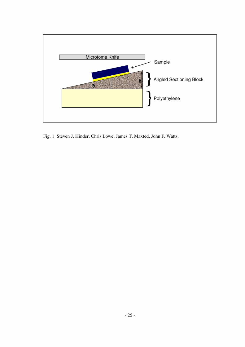
A schematic of the ULAM apparatus as employed in the production of ultra-low-
angle tapers is presented in Fig. 1. The ULAM processing of samples was carried out
on a Microm HM355S motorised rotary microtome (Optech Scientific Instruments,
Thame, UK) equipped with a standard specimen clamp and a tungsten carbide knife.
The ultra-low-angle sectioning blocks (~123mm2
x 7mm) were manufactured in-
house from stainless steel. The ultra-low-angle sectioning blocks have one 123mm2
tapered face raised by a defined amount (in µm) relative to the parallel edge of the
tapered face. The ultra-low-angle sectioning blocks available in our laboratories have
tapered faces raised by a height of 25, 50, 100 & 200µm (parameter h in Fig. 1),
providing taper angles (θ in Fig. 1) of 0.04°, 0.08°, 0.16° & 0.33° respectively .
The following procedure was followed when processing coating samples by the
ULAM technique;
1) A polyethylene (PE) block (~160×160×20 mm) (Aquarius Plastics, Guildford,
UK) was placed in the microtome sample clamp and trimmed with the
tungsten-carbide knife until the sections comprised the complete face of the
PE block. The PE block was then retracted from the knife and double-sided
adhesive tape applied to the freshly trimmed PE block face.
- 10 -
2) The face of an angled sectioning block containing an ultra-low-angle taper
was cleaned with acetone (Fisher Scientific, Loughbrorough, UK) to insure it
was free of any contaminants. Double sided adhesive tape was then applied to
the taper containing face of the angled sectioning block and the specimen to
be processed was applied to the adhesive tape at the centre of the angled
sectioning block face.
3) The angled sectioning block was then secured to the PE block via the double
sided adhesive tape on the trimmed face of the PE block such that the
specimen to be processed wais presented to the microtome knife at an ultra-
low-angle (see Fig. 1).
4) The specimen was then sectioned at between 1 and 5µm sectioning depth
depending on the thickness of the sample coating. Once the desired interface
was revealed or the required depth of tapering obtained the sample was
removed from the angled sectioning block for analysis.
2.3. Scanning Electron Microscopy.
SEM images were acquired on a Hitachi S3200N environmental SEM operated at a
chamber pressure of 50Pa. A 20kV electron beam was employed for scanning to
minimise any possible charging effects.
2.4. Atomic Force Microscopy.

- 11 -
AFM images were acquired on a Digital Instruments Nanoscope III (California, USA)
operated in the tapping mode. Tapered coating samples were fixed to metal AFM
stubs prior to analysis. Ultrasharp Si NSCS11 cantilevers from NT-MDT (Moscow,
Russia) were employed.
2.5. X-ray Photoelectron Spectroscopy.
XPS analyses were performed on a Thermo VG Scientific Sigma Probe spectrometer
(Thermo VG Scientific, East Grinstead, UK). The instrument employs a
monochromated AlKα X-ray source (hν = 1486.6 eV) which was used at 300W (15
kV x 20 mA). The area of analysis was approximately 15µm diameter for the
PVdF/polyurethane interface sample. The pass energy was set at 20eV for high-
resolution spectra of all elements of interest. Charge compensation was achieved
using an electron flood gun.
To aid charge compensation during linescan analysis on the PVdF/PU interface
specimens the linear edge of a Mo grid was positioned such that it was at right angles
to the interface region to be analysed. The Mo grid was held in place by a sprung
Cu/Be clip which was also positioned so as to be at right angle to the interface region
to be analysed. Experience has shown that this combination of Mo grid and Cu/Be
clip geometry promotes stable charge compensation across the interface region to be
investigated.

- 12 -
3. Results and Discussion.
3.1. Ultra-low-angle microtomy.
In a previous paper it was demonstrated that the ultra-low-angle tapers produced from
multilayer, polymeric coating systems by ULAM had application in both ‘buried’
interface analysis and compositional depth profiling by small area X-ray
photoelectron spectroscopy [13]. However, before the ULAM technique can be
accepted for general use two crucial uncertainties need to be resolved. Firstly, what is
the state of the polymeric material along the taper after ULAM processing,
specifically is any roughening or damage of the material surface observed? Secondly,
how well-defined is the interface between the coating layers exposed by ULAM
processing and is there any evidence of smearing of the polymeric material by the
passage of the microtome knife?
The concept behind ULAM is very simple; a specimen is presented to the microtome
knife at an ultra-low-angle (see Fig. 1) such that sectioning of the specimen by the
microtome knife imparts an ultra-low-angle taper through the sample material. To
demonstrate the applicability of ULAM to the investigation of organic materials a
blue PVdF based topcoat formulation and a yellow PU based primer formulation were
employed as a model, multilayer, polymeric coating system. In Fig. 2 a digitally
recorded optical image of a PVdF/PU coating on Al substrate processed by ULAM
such that the interface between the two coatings has been exposed is presented. The
ultra-low-angle taper imparted by ULAM cuts the air/coating surface of the PVdF
- 13 -
topcoat, traverses the bulk of the PVdF topcoat, exposes the PVdF/PU interface
region and terminates in the PU primer bulk (as indicated by the arrow in Fig. 2). The
image in Fig. 2 clearly demonstrates that ULAM is capable of exposing a ‘buried’
interface; in this case the interface is buried below 20µm or more of the PVdF
topcoat.
3.2. Morphology and Topology of Tapered Polymeric Surfaces.
In Fig. 3a an SEM image of a region of the PVdF topcoat bulk exposed by ULAM
processing is presented. The PVdF bulk exposed at the tapered surface in Fig. 3a
exhibits two distinct morphologies. One of the morphological regions is flat and
exhibits a low pixel intensity (dark contrast) in the SEM image. These regions of low
pixel intensity are attributed to regions composed principally of the PVdF polymer
resin. The alternate morphological region of the PVdF taper is granular in nature (the
granules are ~1µm in diameter), a large number of the granules observed in Fig. 3a
are associated with a very high pixel intensity (light contrast). The granules that
exhibit a high pixel intensity are attributed to the presence of pigments in the PVdF
coating formulation. In Fig. 4a a 400µm2 AFM tapping mode image of a region of the
PVdF topcoat bulk exposed by ULAM processing, complementary to the SEM image
of Fig. 3a, is presented. In Fig. 4a the PVdF tapered surface topography reveals the
presence of a large number of polypoid structures, typically 2µm in diameter. Such
polypoid structures have been observed before for both AFM [14] and SEM [15]
characterisation of pristine PVdF film surfaces. However, it is not possible to
categorically assign the polypoid structures observed in Fig. 4a to PVdF alone, a

- 14 -
number of the polypoid structures may be associated with the high pixel intensity
granules observed in Fig. 3a. Surface roughness calculations for the AFM image in
Fig. 4a give Ra = 47 ± 9nm (4µm2 area) suggesting the surface is relatively flat for
one that has been sectioned by a microtome knife. However, this Ra value is much
higher than would be expected for a pristine PVdF film where Ra values <5nm have
been reported [16]. No evidence is observed in Fig. 3a or 4a of any surface damage or
roughening, suggesting that the microtome knife has cleaved the PVdF coating with
minimal perturbation of the polymeric material.
In Fig. 3b an SEM image of a region of the PU primer bulk exposed by ULAM
tapering is presented. It is observed that the morphology exhibited by the tapered PU
surface in Fig. 3b contrasts markedly with that observed for the PVdF region in Fig.
3a. In a manner similar to the PVdF topcoat the PU primer possesses regions of low
pixel intensity (dark contrast) and regions that are granular and which exhibit higher
pixel intensity (light contrast). These regions are attributed to PU polymer rich and
pigment rich regions respectively. However, the PU surface morphology observed in
Fig. 3b also exhibits a large number of needle or acicular structures at or protruding
from the material surface. It is noted that these acicular structures are associated a
with very high pixel intensity (very light contrast) in the SEM image. The observation
of the acicular structures in Fig. 3b is attributed to the presence of strontium-
chromate, in the PU coating. In Fig. 4b a 400µm2 AFM tapping mode image of the
PU primer bulk, complementary to the SEM image in Fig. 3b, is presented. In Fig. 4b
the topography of the PU surface is similar to that observed for the PVdF bulk region
- 15 -
in Fig. 4a. However, the polypoid containing topography observed in Fig. 4b
suggests that in the PU the polypoid structures are more discrete and many stand
proud of or protrude from the sample surface. It is suggested that the polypoid
structures standing proud or protruding from the sample surface are in fact the
acicular structures observed in Fig. 3b. This would correlate with the fact that both
titanium dioxide and barium sulphate, also used in the primer, have primary particle
sizes of around 0.3µm, much smaller than the primary particle size of the strontium
chromate (12-14µm). Calculations of surface roughness obtained from the AFM
image in Fig. 4b give Ra = 51 ± 8nm (4 µm2 area) indicating the surface is flat for one
that has been sectioned by a microtome knife. However, this Ra value is much higher
than would be expected for a pristine PU film where Ra values <2nm (4µm2 area)
have been reported [17]. As with the PVdF bulk region, no evidence is observed in
Fig. 3b or 4b to indicate any damage to or roughening of the sample surface by
tearing or stripping of the polymeric material.
In contrast to the well-ordered sample surfaces observed in Fig. 3a & b the SEM
image in Fig. 3c displays large-scale surface damage leading to considerable surface
roughening due to the tearing and stripping of the polymeric material. The SEM
image in Fig. 3c was acquired on a poorly mounted polyamide/organosilane (PA)
coating that was sectioned with a blunted knife. The damage observed on the PA
coating is directional (that is the damage occurs in a left to right direction in the SEM
image), this direction is consistent with that of the microtome knife as it passed

- 16 -
through the polymeric material. It is also observed in Fig. 3c that some debris
associated with the damage to the PA surface is still resident on the ULAM taper.
3.3. Morphology of Buried Interface Exposed by ULAM.
In Fig. 5a a low resolution SEM image of an interface region between a PVdF based
topcoat (low pixel intensity/dark contrast region in Fig. 5a) and the underlying PU
based primer (higher pixel intensity /light contrast region of Fig. 5a) is presented. The
SEM image in Fig. 5a was acquired on a punched disk sample which upon ULAM
processing commonly produces the curved interface region between the coatings that
is observed in Fig. 5a. The interface region in Fig. 5a, even at low magnification, is
well-defined and exhibits good resolution between the two coating layers. Further
examination of Fig. 5a suggests there is no large scale evidence of smearing of the
polymeric coatings indicating the microtome knife cleaves the coating across the
interface in a precise manner. In contrast to the well-resolved interface region
observed in Fig. 5a the PVdF/PU interface presented in Fig. 5b is poorly defined. The
specimen used to obtain the SEM image in Fig. 5b was prepared from the same
sample panel as the specimen used to obtain the SEM image in Fig. 5a. However, the
specimen used in Fig. 5b was sectioned using a blunted and damaged microtome
knife. In the author’s opinion, the poorly defined PVdF/PU interface and the features
observed at the interface in Fig. 5b result from localised damage to the cutting edge of
the microtome knife. The use of such a knife has resulted in a poorly
resolvedinterface and in the smearing of PVdF topcoat material across the PVdF/PU
interface region into the PU bulk region of the specimen. In practice, the use of a
- 17 -
sharp, pristine microtome knife is essential in ensuring that the exposed ‘buried’
interface exhibits a well-resolved and well-defined boundary between the two coating
layers.
In the discussion above regarding the characterisation of the PVdF and PU surface
morphologies and topologies resulting from ULAM processing it was noted that the
two coating formulations exhibit markedly different morphologies and at a qualitative
level differences in SEM pixel intensity. These differences in morphology and pixel
intensity allow us to readily distinguish the PVdF from the PU across the PVdF/PU
interface observed in Fig. 6. To aid identification of the PVdF/polyurethane interface
broken lines indicating the locus of the interface have been inserted into the SEM
images in Figs. 6a and 6b. In both Fig. 6a and b the low contrast/pixel intensity region
to the left of the PVdF/PU interface is the PVdF topcoat whilst the higher
contrast/pixel intensity region to the right of the interface is the PU primer. The SEM
images of the PVdF/PU interface in Fig. 6 were acquired at higher resolution than
those obtained in Fig. 5. The SEM image in Fig. 6a was acquired at ×350
magnification while that in Fig. 6b was acquired at ×800 magnification. The SEM
images in Figs. 6a and b demonstrate that the PVdF/PU interface is well-defined and
that the two coatings are distinct and readily resolved across the exposed interface.
The higher resolution images in Fig. 6 support the assertion that there is no apparent
evidence of smearing of the two polymeric coatings upon cleavage by the microtome
knife.

- 18 -
3.4. XPS Linescan Analysis of a ‘Buried’ PVdF/PU Interface. ULAM has been applied to the investigation, by XPS linescan, of changes in the
elemental concentration (atomic %) with depth across the interface between a PVdF
topcoat and a PU primer. Before considering this interface, which has been 'buried'
20-25µm below the air/coating surface of the PVdF topcoat, it is instructive to dwell
on the results from the analysis of the bulk sections of both coatings. The
concentration of the fluorine is around 15% whereas a typical surface concentration in
a 70:30 blend of PVdF and acrylic resins is close to 30% demonstrating the
segregation of fluorine containing moieties to the air/coating surface probably as a
result of the natural tendency to reduce surface free energy.
The commercially based formulations chosen for this analysis are known to provide a
strong adhesion between the PVdF based topcoat and the underlying PU based
primer. Changes in the elemental concentration with respect to depth of all the major
constituent elements of the coatings have been followed, the results of which are
presented in Fig. 7. However, minor constituents with concentrations <0.3%
(primarily Sr, Cr & Ba found in the PU primer) have been omitted from Fig. 7. for
reasons of clarity. The initial data obtained from a linescan along a ULAM taper
across a coating/coating interface is that of atomic composition (atomic %) with
horizontal distance. However, with knowledge of the ULAM angle and XPS linescan
step size employed, application of simple geometry (equation 1 below) readily
enables the horizontal distance to be transformed into a depth interval and a chart

- 19 -
describing elemental concentration with depth is readily constructed as is
demonstrated in Fig. 7.
∆z = b tanθ (equation1)
Where ∆z = depth resolution, b = XPS linescan step size, θ = ULAM taper angle. For
the linescan analysis described here the sample was sectioned using the 0.04° taper
angle (θ), a 15µm X-ray spot and a 18µm XPS linescan step size (b) were employed
giving a theoretical depth resolution (∆z) of 13 nm.
In Fig. 7 the results obtained from an XPS linescan analysis detailing changes in the
concentration of C, O, F and N with respect to analysed depth across a buried
PVdF/PU interface are presented. The initial point of analysis in Fig. 7 (depth 0nm) is
within the PVdF bulk whilst the final analysis point (depth 169nm) lies within the PU
bulk. It is observed in Fig 7 that the interface region varies for the different elements.
The interface as defined by fluorine starts at 91nm and ends at 143nm a distance of
52nm. The oxygen interface begins and ends in the same place but the nitrogen
interface only starts at 103nm and ends at 130nm and the carbon interface is even
narrower beginning at 110nm and finishing at 130nm. Thus, elemental concentration
changes attributed to the PVdF/PU interface are observed over depths between 20-
50nm. The data for C in Fig. 7 indicates that there is a small change in the
concentration of C as the analysis traverses the PVdF/PU interface. In the PVdF bulk
region of the taper (0-91nm depth) the concentration of C is ~69% this increases
across the interface region to ~71% in the PU bulk region (130-169nm) of the

- 20 -
analysis. These depth profile concentration values for the bulk regions of the coatings
for C are consistent with XPS reference spectra obtained for the bulk of each coating
formulation. Due to the small differences it is difficult to infer anything significant in
this case. The concentration of F is ~16% in the PVdF bulk; it is observed in Fig. 7
that the concentration of F gradually decreases across the PVdF/PU interface region
(91-130nm) as the ULAM taper results in the thinning of the PVdF topcoat. No signal
for F is observed beyond 143nm (the PU region of the taper sample). The decrease in
the concentration of F is countered by increases in the concentrations of O and N as
observed in Fig. 7. In the PVdF bulk region of the taper the concentrations of O and
N are ~14% and ~1% respectively. The concentration of O and N increase across the
PVdF/PU interface to reach concentration levels of ~24% for O and ~3.2% for N
within the PU bulk. The analysis point at a depth of 130nm suggests there has been
some diffusion of F bearing materials from the PVdF topcoat into the topmost
nanometres of the underlying PU primer [13]. At this analysis point the N
concentration (~3.25 at%) has reached a level consistent with the N signal arising
from the PU bulk; however a residual F signal (~3%) is still observed. This
penetration of the PVdF topcoat into the PU primer may result in the strong adhesion
these coating formulations exhibit towards each other. The oxygen curve
demonstrates the opposite effect and indicates that the oxygen rich species migrate
into the PVdF topcoat thereby widening the interfacial region with the consequence
of further improvement in the interfacial adhesion.

- 21 -
According to geometrical considerations a step change interface can be identified to
within a band 13nm wide. This broadening is a natural consequence of the size of the
small area XPS X-ray spot and its transformation to a depth on the ULAM section. In
practice an interfacial region is defined as the distance over which the concentration
of an element reduces from 84% of its maximum intensity to 16% of that intensity.
That is, one standard deviation either side of the step change position. Thus the
interfacial region is described by the limits 16% and 84% of the change. This is the
usual manner in which interface width, ∆z, is defined in compositional depth profiles
obtained by surface analysis methods. By consideration of the carbon profile obtained
in this work, which will not be greatly affected by interdiffusion of PVdF and PU
(which is at a low level), the depth resolution is estimated at 25nm. The fact that the
depth profiles for carbon, oxygen, nitrogen and fluorine in Fig.7 do not follow each
other in a “mirror like” manner across the interface taken together with the above
hypothesis indicates that the results showing inter-diffusion of fluorine and oxygen
containing moieties in different directions across the interface are highlighting a real
effect.
4. Conclusions.
We have demonstrated by use of a PVdF and PU based model, multilayer, polymeric
coating system that the tapered sample surface, produced by ULAM processing,
exhibits no surface damage or roughening as a result of sectioning with a microtome
knife. Evidence for surface damage and roughening on a polyamide/organosilane
taper surface resulting from incorrect mounting practices and sectioning with a
- 22 -
blunted microtome knife was also demonstrated. Analysis of a PVdF/PU interface
‘buried’ more the 20µm below the PVdF topcoat revealed a well-defined and well-
resolved interface region had been exposed by ULAM processing. No evidence of
sample smearing across the PVdF/PU interface was observed in samples sectioned
with a sharp microtome knife. However, it was demonstrated that samples sectioned
with a blunted and damaged microtome knife possessed poorly resolved interfaces
which also exhibited evidence of polymer smearing. We have also demonstrated by
XPS linescan the applicability of ULAM tapers to compositional depth profiling and
the investigation of ‘buried’ interfaces. Changes in the elemental concentration of C,
O, F and N across a model, multilayer PVdF/PU coating interface were described.
Additionally, the XPS analysis indicated penetration of F bearing components from
the PVdF topcoat into the underlying PU primer. In general, ULAM is readily
capable of producing sample tapers with well-defined geometries and of exposing
‘buried’ interfaces that are well resolved. Although in the studies reported here we
have restricted ULAM processing to polymeric coating materials the technique may
be more generally applied to any material system compatible with being sectioned by
a microtome knife.
Acknowledgements.
The authors gratefully thank Ms Marianne Guichenuy for use of the polyamide/
organosilane SEM image, Dr Peter Zhdan for assistance with AFM image acquisition
and Mr Andy Brown for assistance with SEM image acquisition. The authors
acknowledge the financial support of the EPSRC (Grant no. GR/N65745).

- 23 -
References.
1. CUMPSON PJ. J. Electron Spectrosc. Relat. Phenom. 73 (1995) . : PERRUCHOT
C, WATTS JF, LOWE C, WHITE RG, CUMPSON PJ. Surf. Interf. Anal. 33 (2002)
10.
2. ROSS GJ, BARRADAS NP, HILL MP, JEYNES C, MORRISSEY P, WATTS JF.
J.Mater. Sci. 36 (2001) 4731.
3. GIROIS S, AUDOUIN L, VERDU J, DELPRAT P, MAROT G. Polym. Degrad.
Stab. 51 (1996) 125.
4. ANTON-PRINET C, DUBOIS J, MUR G, GAY M, AUDOUIN L, VERDU J. .
Polym. Degrad. Stab. 60 (1996) 125.
5. ADAMSON K. Prog. Org. Coat. 45 (2002) 69.
6. WALLS JM, HALL DD, SYKES DE Surf. Interf. Anal. 1 (1979) 204.
7. WALLS JM. Thin Solid Films 80 (1981) 213.
8. TARNG ML, FISHER DG. J. Vac. Sci. Technol. 15 (1978) 50.
9. HINTERMANN HE, CHOLLET L. Surface Technology 8 (1979) 421.
10. LEA C, SEAH MP. Thin Solid Films 75 (1981) 67.
11. COHEN JM, CASTLE JE. Inst. Phys. Conf. Ser. No 93 (1988) Chapter 5 275.
12. GUICHENUY M, WATTS JF, ABEL M-L, BROWN AM, AUDENAERT M,
AMOUROUX N. Accepted for publication in Surf. Interf. Anal. August 2004.
13. HINDER SJ, WATTS JF, LOWE C. Accepted for publication in Surf. Interf.
Anal. August 2004.
14. PORTE-DURRIEU MC, AYMES-CHODUR C, VERGNE C, BETZ N,
BAQUEY C. Nucl. Instr. Meth. Phys. Res. B 151 (1999) 404.
154. CHEN N, HONG L. Polymer 43 (2002) 1429.
16. DUCA MD, PLOSCEANU CL, POP T. . Polym. Degrad. Stab.61 (1998) 65.
17.CHUNG T-W, LIU D-Z, WANG S-Y, Wang S-S. Biomaterials 24 (2003) 4655.

- 24 -
Figure Captions.
Fig.1 Schematic depicting the concept of ultra-low-angle microtomy operation.
Fig.2 A digitally recorded optical image of a PVdF/poly(urethane) multilayer coating
interface exposed by ultra-low-angle microtomy. The blue regions is the PVdF based
topcoat whilst the yellow region is the polyurethane based primer. The arrow
indicates the direction followed by the ultra-low-angle taper imparted by ULAM
processing.
Fig. 3 SEM images of polymer coating bulk acquired on tapers produced by ultra-
low-angle microtomy. a) PVdF bulk, b) polyurethane bulk, c) polyamide/organosilane
bulk.
Fig. 4 Atomic force microscopy tapping mode images, 400µm2, of (a) the
poly(vinylidene difluoride) region and (b) the poly(urethane) region of a ULAM
tapered PVdF/PU sample.
Fig. 5 SEM low resolution images of the PVdF/polyurethane interface exposed by
ultra-low-angle microtomy. a) PVdF/polyurethane interface exposed by a sharp
microtome knife, b) PVdF/polyurethane interface exposed by a blunted and pitted
microtome knife.
Figure 6. SEM images of the PVdF/polyurethane interface exposed by ultra-low-
angle microtomy. a) PVdF/polyurethane interface, b) the same interface at higher
resolution. The broken lines indicate the locus of the interface between the PVdF
topcoat and the polyurethane primer.
Fig. 7. Changes in C, O, F and N concentration traversing a ULAM produced taper
exposing a ‘buried’ PVdF/PU interface region. The taper was cut using a 0.04° angle,
a 15µm X-ray spot size and a 18µm linescan step size were employed, thus,
theoretically, each successive analysis point increases the analysed depth by 13nm.
The values of the N1s data series have been multiplied by a factor of 10 for reasons of
clarity.
- 25 -
Fig. 1 Steven J. Hinder, Chris Lowe, James T. Maxted, John F. Watts.
h
Polyethylene B
Angled Sectioning Block
Sample
h h
}}
θ θ θ
Microtome Knife

- 26 -
Fig. 2 Steven J Hinder, Chris Lowe, James T. Maxted, John F. Watts.

- 27 -
a)
b)
c)
Fig. 3 Steven J. Hinder, Chris Lowe, James T. Maxted, John F. Watts.
25µm25µm25µm
25µm25µm25µm

- 28 -
a)
b)
b)
Fig. 4 Steven J. Hinder, Chris Lowe, James T. Maxted, John F. Watts.

- 29 -
a)
b)
Fig. 5 Steven J. Hinder, Chris Lowe, James T. Maxted, John F. Watts.
1mm
1mm

- 30 -
a)
b)
Fig. 6 Steven J. Hinder, Chris Lowe, James T. Maxted, John F. Watts.
100µm
50µm

- 31 -
Fig. 7 Steven J. Hinder, Chris Lowe, James T. Maxted, John F. Watts.
0
10
20
30
40
50
60
70
80
0 20 40 60 80 100 120 140 160
Depth / nm
Co
ncen
trat
ion
/ A
tom
ic %
C1s
O1s
N1s x10
F1s