The Main Memory System: Challenges and Opportunitiesomutlu/pub/main-memory-system_kiise15.… · 16...
26
16 특집원고Ⅰ The Main Memory System: Challenges and Opportunities The Main Memory System: Challenges and Opportunities Carnegie Mellon University Onur Mutlu・ Justin Meza・ Lavanya Subramanian The memory system is a fundamental performance and energy bottleneck in almost all computing systems. Recent system design, application, and technology trends that require more capacity, bandwidth, efficiency, and predictability out of the memory system make it an even more important system bottleneck. At the same time, DRAM technology is experiencing difficult technology scaling challenges that make the maintenance and enhancement of its capacity, energy-efficiency, and reliability significantly more costly with conventional techniques. In this article, after describing the demands and challenges faced by the memory system, we examine some promising research and design directions to overcome challenges posed by memory scaling. Specifically, we describe three major new research challenges and solution directions: 1) enabling new DRAM architectures, functions, interfaces, and better integration of the DRAM and the rest of the system (an approach we call system-DRAM co-design), 2) designing a memory system that employs emerging non-volatile memory technologies and takes advantage of multiple different technologies (i.e., hybrid memory systems), 3) providing predictable performance and QoS to applications sharing the memory system (i.e., QoS-aware memory systems ). We also briefly describe our ongoing related work in combating scaling challenges of NAND flash memory. Keywords: Memory systems, scaling, DRAM, flash, non-volatile memory, QoS, reliability, hybrid memory, storage 1. Introduction Main memory is a critical component of all computing systems, employed in server, embedded, desktop, mobile and sensor environments. Memory capacity, energy, cost, performance, and management algorithms must scale as we scale the size of the computing system in order to maintain performance growth and enable new applications. Unfortunately, such scaling has become difficult because recent trends in systems, applications, and technology greatly exacerbate the memory system bottleneck. 2. Memory System Trends In particular, on the systems/architecture front, energy and power consumption have become key design limiters as the memory system continues to be responsible for a significant fraction of overall system energy/power [109]. More and increasingly heterogeneous processing cores and agents/clients are sharing the memory system [9, 33, 176, 179, 75, 76, 58, 37], leading to increasing demand for memory capacity and bandwidth along with a relatively new demand for predictable performance and quality of service (QoS) from the memory system [126, 134, 174]. On the applications front, important applications are usually very data intensive and are becoming increasingly so [15], requiring both real-time and offline manipulation of great amounts of data. For example, next-generation genome sequencing technologies produce massive amounts of sequence data that overwhelms memory storage and bandwidth requirements of today's high-end desktop and laptop systems [184, 7, 195, 108] yet researchers have the goal of enabling low-cost personalized medicine, which requires even more data and its effective analyses. Creation of new killer applications and usage models for computers likely depends on how well the memory system can support the efficient storage and manipulation of data in such data-intensive applications. In addition, there is an increasing trend towards consolidation of applications on a chip to improve efficiency, which leads to the sharing of the memory system across many heterogeneous applications 특집원고Ⅰ
-
Upload
trinhthuan -
Category
Documents
-
view
214 -
download
0
Transcript of The Main Memory System: Challenges and Opportunitiesomutlu/pub/main-memory-system_kiise15.… · 16...
16 특집원고Ⅰ The Main Memory System: Challenges and Opportunities
The Main Memory System: Challenges and Opportunities
Carnegie Mellon University Onur Mutlu・Justin Meza・Lavanya Subramanian
The memory system is a fundamental performance and energy bottleneck in almost all computing systems. Recent system design, application, and technology trends that require more capacity, bandwidth, efficiency, and predictability out of the memory system make it an even more important system bottleneck. At the same time, DRAM technology is experiencing difficult technology scaling challenges that make the maintenance and enhancement of its capacity, energy-efficiency, and reliability significantly more costly with conventional techniques.
In this article, after describing the demands and challenges faced by the memory system, we examine some promising research and design directions to overcome challenges posed by memory scaling. Specifically, we describe three major new research challenges and solution directions: 1) enabling new DRAM architectures, functions, interfaces, and better integration of the DRAM and the rest of the system (an approach we call system-DRAM co-design), 2) designing a memory system that employs emerging non-volatile memory technologies and takes advantage of multiple different technologies (i.e., hybrid memory systems), 3) providing predictable performance and QoS to applications sharing the memory system (i.e., QoS-aware memory systems). We also briefly describe our ongoing related work in combating scaling challenges of NAND flash memory.Keywords: Memory systems, scaling, DRAM, flash, non-volatile memory, QoS, reliability, hybrid memory, storage
1. Introduction
Main memory is a critical component of all computing systems, employed in server, embedded, desktop, mobile and sensor environments. Memory capacity, energy, cost, performance, and management algorithms must scale as
we scale the size of the computing system in order to maintain performance growth and enable new applications. Unfortunately, such scaling has become difficult because recent trends in systems, applications, and technology greatly exacerbate the memory system bottleneck.
2. Memory System Trends
In particular, on the systems/architecture front, energy and power consumption have become key design limiters as the memory system continues to be responsible for a significant fraction of overall system energy/power [109]. More and increasingly heterogeneous processing cores and agents/clients are sharing the memory system [9, 33, 176, 179, 75, 76, 58, 37], leading to increasing demand for memory capacity and bandwidth along with a relatively new demand for predictable performance and quality of service (QoS) from the memory system [126, 134, 174].
On the applications front, important applications are usually very data intensive and are becoming increasingly so [15], requiring both real-time and offline manipulation of great amounts of data. For example, next-generation genome sequencing technologies produce massive amounts of sequence data that overwhelms memory storage and bandwidth requirements of today's high-end desktop and laptop systems [184, 7, 195, 108] yet researchers have the goal of enabling low-cost personalized medicine, which requires even more data and its effective analyses. Creation of new killer applications and usage models for computers likely depends on how well the memory system can support the efficient storage and manipulation of data in such data-intensive applications. In addition, there is an increasing trend towards consolidation of applications on a chip to improve efficiency, which leads to the sharing of the memory system across many heterogeneous applications
특집원고Ⅰ
2015. 2 정보과학회지 17
with diverse performance requirements, exacerbating the aforementioned need for predictable performance guarantees from the memory system [174, 180].
On the technology front, two major trends profoundly affect memory systems. First, there is increasing difficulty scaling the well-established charge-based memory technologies, such as DRAM [121, 87, 67, 8, 99, 2, 93] and flash memory [94, 120, 18, 19, 22], to smaller technology nodes [130, 131]. Such scaling has enabled memory systems with reasonable capacity and efficiency; lack of it will make it difficult to achieve high capacity and efficiency at low cost. Challenges with DRAM scaling were recently highlighted by a paper written by Samsung and Intel [80]. Second, some emerging resistive memory technologies, such as phase change memory (PCM) [161, 191, 99, 100, 157], spin-transfer torque magnetic memory (STT-MRAM) [29, 97] or resistive RAM (RRAM) [192] appear more scalable, have latency and bandwidth characteristics much closer to DRAM than flash memory and hard disks, and are non-volatile with little idle power consumption. Such emerging technologies can enable new opportunities in system design, including, for example, the unification of memory and storage subsystems [124]. They have the potential to be employed as part of main memory, alongside or in place of less scalable and leaky DRAM, but they also have various shortcomings depending on the technology (e.g., some have cell endurance problems, some have very high write latency/power, some have low density) that need to be overcome or tolerated.
3. Memory System Requirements
System architects and users have always wanted more from the memory system: high performance (ideally, zero latency and infinite bandwidth), infinite capacity, all at zero cost! The aforementioned trends do not only exacerbate and morph the above requirements, but also add some new requirements. We classify the requirements from the memory system into two categories: exacerbated traditional requirements and (relatively) new requirements.
The traditional requirements of performance, capacity, and cost are greatly exacerbated today due to increased pressure on the memory system, consolidation of multiple applications/agents sharing the memory system, and difficulties in DRAM technology and density scaling. In
terms of performance, two aspects have changed. First, today's systems and applications not only require low latency and high bandwidth (as traditional memory systems have been optimized for), but they also require new techniques to manage and control memory interference between different cores, agents, and applications that share the memory system [126, 134, 174, 38, 180] in order to provide high system performance as well as predictable performance (or quality of service) to different applications [174]. Second, there is a need for increased memory bandwidth for many applications as the placement of more cores and agents on chip make the memory pin bandwidth an increasingly precious resource that determines system performance [68], especially for memory-bandwidth-intensive workloads, such as GPGPUs [78, 77], heterogeneous systems [9], and consolidated workloads [134, 71, 70]. In terms of capacity, the need for memory capacity is greatly increasing due to the placement of multiple data-intensive applications on the same chip and continued increase in the data sets of important applications. One recent work showed that given that the core count is increasing at a faster rate than DRAM capacity, the expected memory capacity per core is to drop by 30% every two years [110], an alarming trend since much of today's software innovations and features rely on increased memory capacity. In terms of cost, increasing difficulty in DRAM technology scaling poses a difficult challenge to building higher density (and, as a result, lower cost) main memory systems. Similarly, cost-effective options for providing high reliability and increasing memory bandwidth are needed to scale the systems proportionately with the reliability and data throughput needs of today's data-intensive applications. Hence, the three traditional requirements of performance, capacity, and cost have become exacerbated.
The relatively new requirements from the main memory system are threefold. First, technology scalability: there is a new need for finding a technology that is much more scalable than DRAM in terms of capacity, energy, and cost, as described earlier. As DRAM continued to scale well from the above-100-nm to 30-nm technology nodes, the need for finding a more scalable technology was not a prevalent problem. Today, with the significant circuit and device scaling challenges DRAM has been facing below the 30-nm node [80], it is. Second, there is a relatively new need for providing performance predictability and
18 특집원고Ⅰ The Main Memory System: Challenges and Opportunities
QoS in the shared main memory system. As single-core systems were dominant and memory bandwidth and capacity were much less of a shared resource in the past, the need for predictable performance was much less apparent or prevalent [126]. Today, with increasingly more cores/agents on chip sharing the memory system and increasing amounts of workload consolidation, memory fairness, predictable memory performance, and techniques to mitigate memory interference have become first-class design constraints. Third, there is a great need for much higher energy/power/bandwidth efficiency in the design of the main memory system. Higher efficiency in terms of energy, power, and bandwidth enables the design of much more scalable systems where main memory is shared between many agents, and can enable new applications in almost all domains where computers are used. Arguably, this is not a new need today, but we believe it is another first-class design constraint that has not been as traditional as performance, capacity, and cost.
4. Solution Directions and Research Opportunities
As a result of these systems, applications, and technology trends and the resulting requirements, it is our position that researchers and designers need to fundamentally rethink the way we design memory systems today to 1) overcome scaling challenges with DRAM, 2) enable the use of emerging memory technologies, 3) design memory systems that provide predictable performance and quality of service to applications and users. The rest of this article describes our solution ideas in these three relatively new research directions, with pointers to specific techniques when possible.1) Since scaling challenges themselves arise due to difficulties in enhancing memory components at solely
1) Note that this paper is not meant or designed to be a survey of all recent works in the field of memory systems. There are many such insightful works, but we do not have space in this paper to discuss them all. This paper is meant to outline the challenges and research directions in memory systems as we see them. Therefore, many of the solutions we discuss draw heavily upon our own past, current, and future research. We believe this will be useful for the community as the directions we have pursued and are pursuing are hopefully fundamental challenges for which other solutions and approaches would be greatly useful to develop. We look forward to similar papers from other researchers describing their perspectives and solution directions/ideas.
one level of the computing stack (e.g., the device and/or circuit levels in case of DRAM scaling), we believe effective solutions to the above challenges will require cooperation across different layers of the computing stack, from algorithms to software to microarchitecture to devices, as well as between different components of the system, including processors, memory controllers, memory chips, and the storage subsystem. As much as possible, we will give examples of such cross-layer solutions and directions.
5. New Research Challenge 1:New DRAM Architectures
DRAM has been the choice technology for implementing main memory due to its relatively low latency and low cost. DRAM process technology scaling has for long enabled lower cost per unit area by enabling reductions in DRAM cell size. Unfortunately, further scaling of DRAM cells has become costly [8, 121, 87, 67, 99, 2, 80] due to increased manufacturing complexity/cost, reduced cell reliability, and potentially increased cell leakage leading to high refresh rates. Recently, a paper by Samsung and Intel [80] also discussed the key scaling challenges of DRAM at the circuit level. They have identified three major challenges as impediments to effective scaling of DRAM to smaller technology nodes: 1) the growing cost of refreshes [111], 2) increase in write latency, and 3) variation in the retention time of a cell over time [112]. In light of such challenges, we believe there are at least the following key issues to tackle in order to design new DRAM architectures that are much more scalable:
1) reducing the negative impact of refresh on energy, performance, QoS, and density scaling [111, 112, 26, 83, 80],
2) improving reliability of DRAM at low cost [143, 119, 93, 83],
3) improving DRAM parallelism/bandwidth [92, 26], latency [106, 107], and energy efficiency [92, 106, 111, 185].
4) minimizing data movement between DRAM and processing elements, which causes high latency, energy, and bandwidth consumption, by doing more operations on the DRAM and the memory controllers [165],
5) reducing the significant amount of waste present in
2015. 2 정보과학회지 19
today's main memories in which much of the fetched/stored data can be unused due to coarse- granularity management [123, 197, 151, 152, 185, 153].
Traditionally, DRAM devices have been separated from the rest of the system with a rigid interface, and DRAM has been treated as a passive slave device that simply responds to the commands given to it by the memory controller. We believe the above key issues can be solved more easily if we rethink the DRAM architecture and functions, and redesign the interface such that DRAM, controllers, and processors closely cooperate. We call this high-level solution approach system-DRAM co-design. We believe key technology trends, e.g., the 3D stacking of memory and logic [115, 3, 186] and increasing cost of scaling DRAM solely via circuit-level approaches [121, 87, 67, 80], enable such a co-design to become increasingly more feasible. We proceed to provide several examples from our recent research that tackle the problems of refresh (and retention errors), reliability, parallelism, latency, energy efficiency, in-memory computation, and capacity and bandwidth waste.
5.1 Reducing Refresh Impact
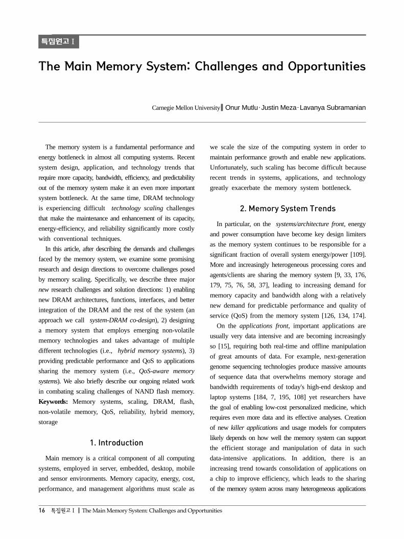
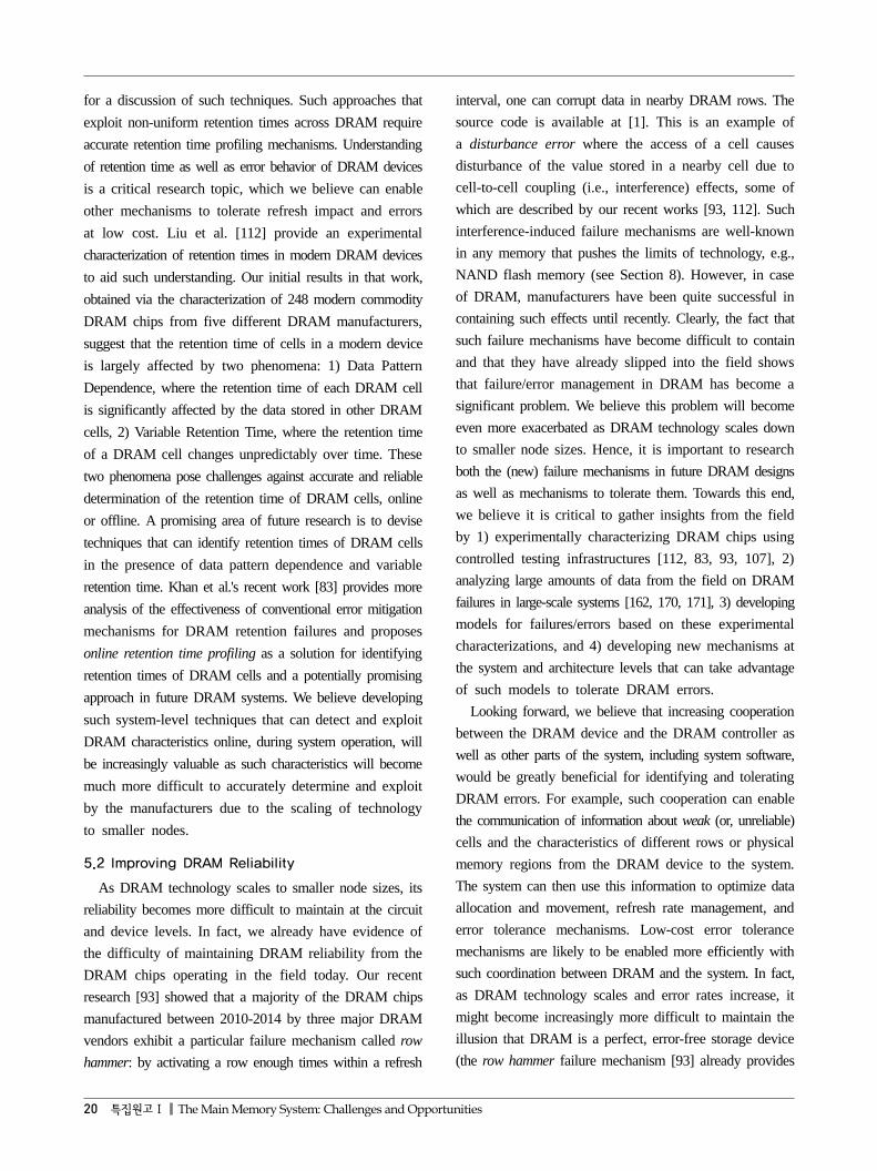
With higher DRAM capacity, more cells need to be refreshed at likely higher rates than today. Our recent work [111] indicates that refresh rate limits DRAM density scaling: a hypothetical 64Gb DRAM device would spend 46% of its time and 47% of all DRAM energy for refreshing its rows, as opposed to typical 4Gb devices of today that spend 8% of the time and 15% of the DRAM energy on refresh (as shown in Figure 1). For instance, a modern supercomputer may have 1PB of memory in total [4]. If we assume this memory is built from 8Gb DRAM devices and a nominal refresh rate, 7.8kW of power would be expended, on average, just to refresh the entire 1PB memory. This is quite a large number, just to ensure the memory correctly keeps its contents! And, this power is always spent regardless of how much the supercomputer is utilized.
Today's DRAM devices refresh all rows at the same worst-case rate (e.g., every 64ms). However, only a small number of weak rows require a high refresh rate [88, 112, 83] (e.g., only~1000 rows in 32GB DRAM require to be refreshed more frequently than every 256ms). Retention- Aware Intelligent DRAM Refresh (RAIDR) [111] exploits this observation: it groups DRAM rows into bins (implemented
as Bloom filters [14] to minimize hardware overhead) based on the retention time of the weakest cell within each row. Each row is refreshed at a rate corresponding to its retention time bin. Since few rows need high refresh rate, one can use very few bins to achieve large reductions in refresh counts: our results show that RAIDR with three bins (1.25KB hardware cost) reduces refresh operations by ~75% leading to significant improvements in system performance and energy efficiency as described by Liu et al. [111].
Like RAIDR, other approaches have also been proposed to take advantage of the retention time variation of cells across a DRAM chip. For example, some works proposed refreshing weak rows more frequently at a per-row granularity, others proposed not using memory rows with low retention times, and yet others suggested mapping critical data to cells with longer retention times such that critical data is not lost [188, 69, 114, 147, 86, 5] – see [111, 112]
(a) Power consumption
(b) Throughput Loss
Fig. 1 Impact of refresh in current (DDR3) and projected
DRAM devices. Reproduced from [111].
20 특집원고Ⅰ The Main Memory System: Challenges and Opportunities
for a discussion of such techniques. Such approaches that exploit non-uniform retention times across DRAM require accurate retention time profiling mechanisms. Understanding of retention time as well as error behavior of DRAM devices is a critical research topic, which we believe can enable other mechanisms to tolerate refresh impact and errors at low cost. Liu et al. [112] provide an experimental characterization of retention times in modern DRAM devices to aid such understanding. Our initial results in that work, obtained via the characterization of 248 modern commodity DRAM chips from five different DRAM manufacturers, suggest that the retention time of cells in a modern device is largely affected by two phenomena: 1) Data Pattern Dependence, where the retention time of each DRAM cell is significantly affected by the data stored in other DRAM cells, 2) Variable Retention Time, where the retention time of a DRAM cell changes unpredictably over time. These two phenomena pose challenges against accurate and reliable determination of the retention time of DRAM cells, online or offline. A promising area of future research is to devise techniques that can identify retention times of DRAM cells in the presence of data pattern dependence and variable retention time. Khan et al.'s recent work [83] provides more analysis of the effectiveness of conventional error mitigation mechanisms for DRAM retention failures and proposes online retention time profiling as a solution for identifying retention times of DRAM cells and a potentially promising approach in future DRAM systems. We believe developing such system-level techniques that can detect and exploit DRAM characteristics online, during system operation, will be increasingly valuable as such characteristics will become much more difficult to accurately determine and exploit by the manufacturers due to the scaling of technology to smaller nodes.
5.2 Improving DRAM Reliability
As DRAM technology scales to smaller node sizes, its reliability becomes more difficult to maintain at the circuit and device levels. In fact, we already have evidence of the difficulty of maintaining DRAM reliability from the DRAM chips operating in the field today. Our recent research [93] showed that a majority of the DRAM chips manufactured between 2010-2014 by three major DRAM vendors exhibit a particular failure mechanism called row hammer: by activating a row enough times within a refresh
interval, one can corrupt data in nearby DRAM rows. The source code is available at [1]. This is an example of a disturbance error where the access of a cell causes disturbance of the value stored in a nearby cell due to cell-to-cell coupling (i.e., interference) effects, some of which are described by our recent works [93, 112]. Such interference-induced failure mechanisms are well-known in any memory that pushes the limits of technology, e.g., NAND flash memory (see Section 8). However, in case of DRAM, manufacturers have been quite successful in containing such effects until recently. Clearly, the fact that such failure mechanisms have become difficult to contain and that they have already slipped into the field shows that failure/error management in DRAM has become a significant problem. We believe this problem will become even more exacerbated as DRAM technology scales down to smaller node sizes. Hence, it is important to research both the (new) failure mechanisms in future DRAM designs as well as mechanisms to tolerate them. Towards this end, we believe it is critical to gather insights from the field by 1) experimentally characterizing DRAM chips using controlled testing infrastructures [112, 83, 93, 107], 2) analyzing large amounts of data from the field on DRAM failures in large-scale systems [162, 170, 171], 3) developing models for failures/errors based on these experimental characterizations, and 4) developing new mechanisms at the system and architecture levels that can take advantage of such models to tolerate DRAM errors.
Looking forward, we believe that increasing cooperation between the DRAM device and the DRAM controller as well as other parts of the system, including system software, would be greatly beneficial for identifying and tolerating DRAM errors. For example, such cooperation can enable the communication of information about weak (or, unreliable) cells and the characteristics of different rows or physical memory regions from the DRAM device to the system. The system can then use this information to optimize data allocation and movement, refresh rate management, and error tolerance mechanisms. Low-cost error tolerance mechanisms are likely to be enabled more efficiently with such coordination between DRAM and the system. In fact, as DRAM technology scales and error rates increase, it might become increasingly more difficult to maintain the illusion that DRAM is a perfect, error-free storage device (the row hammer failure mechanism [93] already provides
2015. 2 정보과학회지 21
evidence for this). DRAM may start looking increasingly like flash memory, where the memory controller manages errors such that an acceptable specified uncorrectable bit error rate is satisfied [18, 20]. We envision a DRAM Translation Layer (DTL), not unlike the Flash Translation Layer (FTL) of today in spirit (which is decoupled from the processor and performs a wide variety of management functions for flash memory, including error correction, garbage collection, read/write scheduling, data mapping, etc.), can enable better scaling of DRAM memory into the future by not only enabling easier error management but also opening up new opportunities to perform computation, mapping and metadata management close to memory. This can become especially feasible in the presence of the trend of combining the DRAM controller and DRAM via 3D stacking. What should the interface be to such a layer and what should be performed in the DTL are promising areas of future research.
5.3 Improving DRAM Parallelism
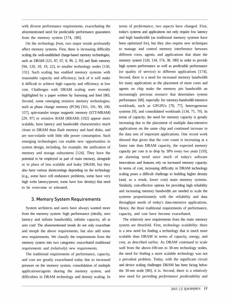
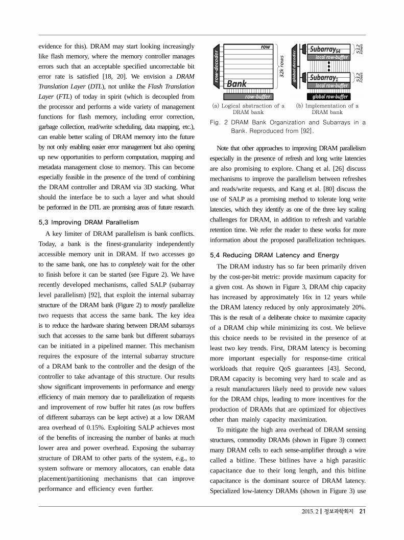
A key limiter of DRAM parallelism is bank conflicts. Today, a bank is the finest-granularity independently accessible memory unit in DRAM. If two accesses go to the same bank, one has to completely wait for the other to finish before it can be started (see Figure 2). We have recently developed mechanisms, called SALP (subarray level parallelism) [92], that exploit the internal subarray structure of the DRAM bank (Figure 2) to mostly parallelize two requests that access the same bank. The key idea is to reduce the hardware sharing between DRAM subarrays such that accesses to the same bank but different subarrays can be initiated in a pipelined manner. This mechanism requires the exposure of the internal subarray structure of a DRAM bank to the controller and the design of the controller to take advantage of this structure. Our results show significant improvements in performance and energy efficiency of main memory due to parallelization of requests and improvement of row buffer hit rates (as row buffers of different subarrays can be kept active) at a low DRAM area overhead of 0.15%. Exploiting SALP achieves most of the benefits of increasing the number of banks at much lower area and power overhead. Exposing the subarray structure of DRAM to other parts of the system, e.g., to system software or memory allocators, can enable data placement/partitioning mechanisms that can improve performance and efficiency even further.
(a) Logical abstraction of a DRAM bank
(b) Implementation of a
DRAM bank
Fig. 2 DRAM Bank Organization and Subarrays in a
Bank. Reproduced from [92].
Note that other approaches to improving DRAM parallelism especially in the presence of refresh and long write latencies are also promising to explore. Chang et al. [26] discuss mechanisms to improve the parallelism between refreshes and reads/write requests, and Kang et al. [80] discuss the use of SALP as a promising method to tolerate long write latencies, which they identify as one of the three key scaling challenges for DRAM, in addition to refresh and variable retention time. We refer the reader to these works for more information about the proposed parallelization techniques.
5.4 Reducing DRAM Latency and Energy
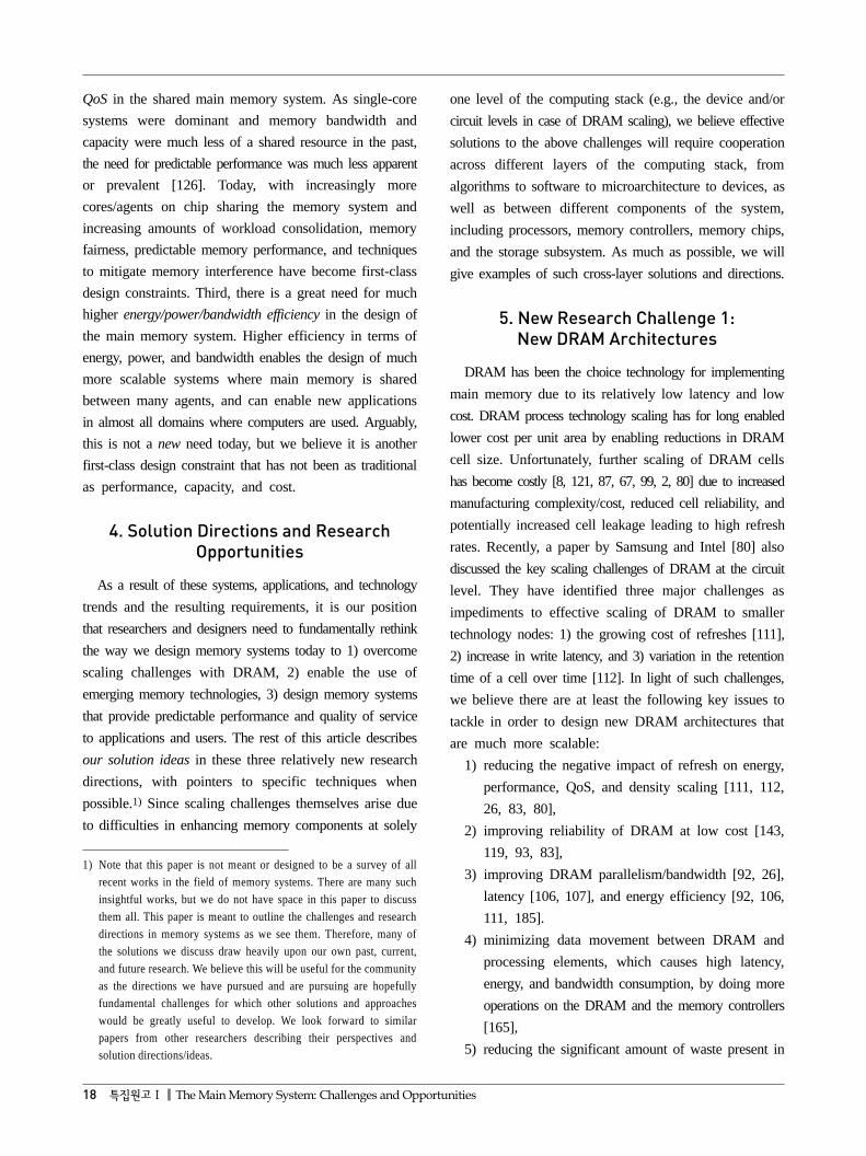
The DRAM industry has so far been primarily driven by the cost-per-bit metric: provide maximum capacity for a given cost. As shown in Figure 3, DRAM chip capacity has increased by approximately 16x in 12 years while the DRAM latency reduced by only approximately 20%. This is the result of a deliberate choice to maximize capacity of a DRAM chip while minimizing its cost. We believe this choice needs to be revisited in the presence of at least two key trends. First, DRAM latency is becoming more important especially for response-time critical workloads that require QoS guarantees [43]. Second, DRAM capacity is becoming very hard to scale and as a result manufacturers likely need to provide new values for the DRAM chips, leading to more incentives for the production of DRAMs that are optimized for objectives other than mainly capacity maximization.
To mitigate the high area overhead of DRAM sensing structures, commodity DRAMs (shown in Figure 3) connect many DRAM cells to each sense-amplifier through a wire called a bitline. These bitlines have a high parasitic capacitance due to their long length, and this bitline capacitance is the dominant source of DRAM latency. Specialized low-latency DRAMs (shown in Figure 3) use
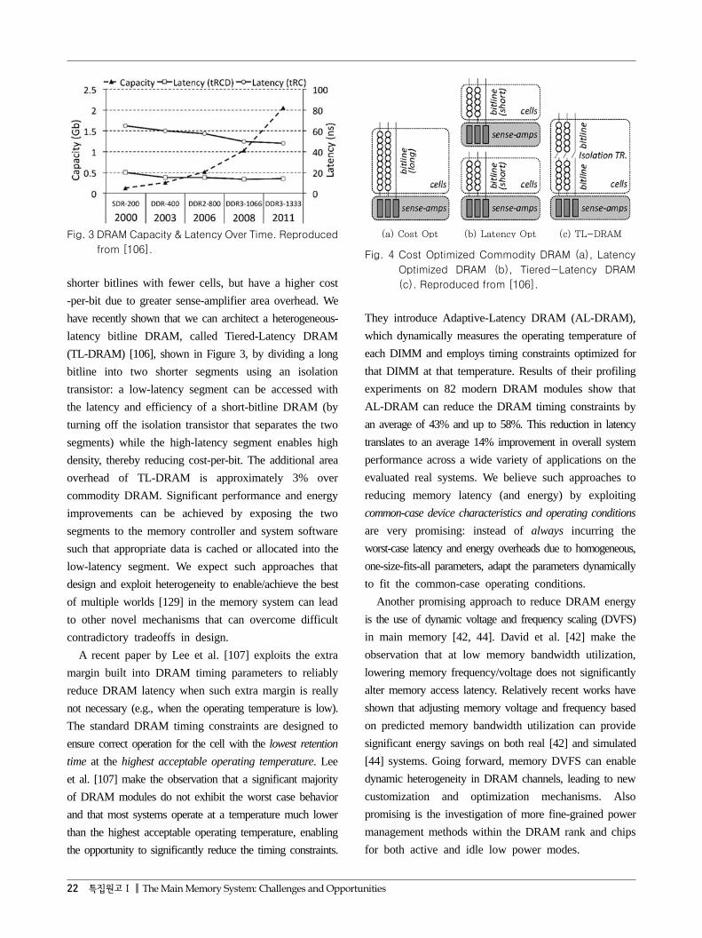
22 특집원고Ⅰ The Main Memory System: Challenges and Opportunities
Fig. 3 DRAM Capacity & Latency Over Time. Reproduced
from [106].
shorter bitlines with fewer cells, but have a higher cost -per-bit due to greater sense-amplifier area overhead. We have recently shown that we can architect a heterogeneous- latency bitline DRAM, called Tiered-Latency DRAM (TL-DRAM) [106], shown in Figure 3, by dividing a long bitline into two shorter segments using an isolation transistor: a low-latency segment can be accessed with the latency and efficiency of a short-bitline DRAM (by turning off the isolation transistor that separates the two segments) while the high-latency segment enables high density, thereby reducing cost-per-bit. The additional area overhead of TL-DRAM is approximately 3% over commodity DRAM. Significant performance and energy improvements can be achieved by exposing the two segments to the memory controller and system software such that appropriate data is cached or allocated into the low-latency segment. We expect such approaches that design and exploit heterogeneity to enable/achieve the best of multiple worlds [129] in the memory system can lead to other novel mechanisms that can overcome difficult contradictory tradeoffs in design.
A recent paper by Lee et al. [107] exploits the extra margin built into DRAM timing parameters to reliably reduce DRAM latency when such extra margin is really not necessary (e.g., when the operating temperature is low). The standard DRAM timing constraints are designed to ensure correct operation for the cell with the lowest retention time at the highest acceptable operating temperature. Lee et al. [107] make the observation that a significant majority of DRAM modules do not exhibit the worst case behavior and that most systems operate at a temperature much lower than the highest acceptable operating temperature, enabling the opportunity to significantly reduce the timing constraints.
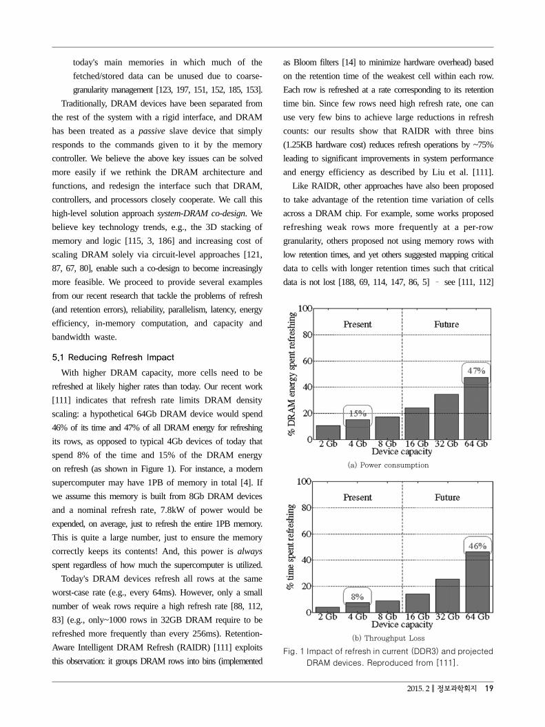
(a) Cost Opt
(b) Latency Opt
(c) TL-DRAM
Fig. 4 Cost Optimized Commodity DRAM (a), Latency
Optimized DRAM (b), Tiered-Latency DRAM
(c). Reproduced from [106].
They introduce Adaptive-Latency DRAM (AL-DRAM), which dynamically measures the operating temperature of each DIMM and employs timing constraints optimized for that DIMM at that temperature. Results of their profiling experiments on 82 modern DRAM modules show that AL-DRAM can reduce the DRAM timing constraints by an average of 43% and up to 58%. This reduction in latency translates to an average 14% improvement in overall system performance across a wide variety of applications on the evaluated real systems. We believe such approaches to reducing memory latency (and energy) by exploiting common-case device characteristics and operating conditions are very promising: instead of always incurring the worst-case latency and energy overheads due to homogeneous, one-size-fits-all parameters, adapt the parameters dynamically to fit the common-case operating conditions.
Another promising approach to reduce DRAM energy is the use of dynamic voltage and frequency scaling (DVFS) in main memory [42, 44]. David et al. [42] make the observation that at low memory bandwidth utilization, lowering memory frequency/voltage does not significantly alter memory access latency. Relatively recent works have shown that adjusting memory voltage and frequency based on predicted memory bandwidth utilization can provide significant energy savings on both real [42] and simulated [44] systems. Going forward, memory DVFS can enable dynamic heterogeneity in DRAM channels, leading to new customization and optimization mechanisms. Also promising is the investigation of more fine-grained power management methods within the DRAM rank and chips for both active and idle low power modes.
2015. 2 정보과학회지 23
5.5 Exporting Bulk Data Operations to DRAM:
Enabling In-Memory Computation
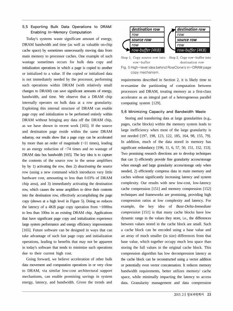
Today's systems waste significant amount of energy, DRAM bandwidth and time (as well as valuable on-chip cache space) by sometimes unnecessarily moving data from main memory to processor caches. One example of such wastage sometimes occurs for bulk data copy and initialization operations in which a page is copied to another or initialized to a value. If the copied or initialized data is not immediately needed by the processor, performing such operations within DRAM (with relatively small changes to DRAM) can save significant amounts of energy, bandwidth, and time. We observe that a DRAM chip internally operates on bulk data at a row granularity. Exploiting this internal structure of DRAM can enable page copy and initialization to be performed entirely within DRAM without bringing any data off the DRAM chip, as we have shown in recent work [165]. If the source and destination page reside within the same DRAM subarray, our results show that a page copy can be accelerated by more than an order of magnitude (~11 times), leading to an energy reduction of ~74 times and no wastage of DRAM data bus bandwidth [165]. The key idea is to capture the contents of the source row in the sense amplifiers by by 1) activating the row, then 2) deactivating the source row (using a new command which introduces very little hardware cost, amounting to less than 0.03% of DRAM chip area), and 3) immediately activating the destination row, which causes the sense amplifiers to drive their contents into the destination row, effectively accomplishing the page copy (shown at a high level in Figure 5). Doing so reduces the latency of a 4KB page copy operation from ~1000ns to less than 100ns in an existing DRAM chip. Applications that have significant page copy and initialization experience large system performance and energy efficiency improvements [165]. Future software can be designed in ways that can take advantage of such fast page copy and initialization operations, leading to benefits that may not be apparent in today's software that tends to minimize such operations due to their current high cost.
Going forward, we believe acceleration of other bulk data movement and computation operations in or very close to DRAM, via similar low-cost architectural support mechanisms, can enable promising savings in system energy, latency, and bandwidth. Given the trends and
Step 1. Copy source row into
row-buffer
Step 2. Copy row-buffer into
destination row
Fig. 5 High-level idea behind RowClone's in-DRAM page
copy mechanism.
requirements described in Section 2, it is likely time to re-examine the partitioning of computation between processors and DRAM, treating memory as a first-class accelerator as an integral part of a heterogeneous parallel computing system [129].
5.6 Minimizing Capacity and Bandwidth Waste
Storing and transferring data at large granularities (e.g., pages, cache blocks) within the memory system leads to large inefficiency when most of the large granularity is not needed [197, 198, 123, 122, 185, 164, 98, 155, 79]. In addition, much of the data stored in memory has significant redundancy [196, 11, 6, 57, 50, 151, 152, 153]. Two promising research directions are to develop techniques that can 1) efficiently provide fine granularity access/storage when enough and large granularity access/storage only when needed, 2) efficiently compress data in main memory and caches without significantly increasing latency and system complexity. Our results with new low-cost, low-latency cache compression [151] and memory compression [152] techniques and frameworks are promising, providing high compression ratios at low complexity and latency. For example, the key idea of Base-Delta-Immediate compression [151] is that many cache blocks have low dynamic range in the values they store, i.e., the differences between values stored in the cache block are small. Such a cache block can be encoded using a base value and an array of much smaller (in size) differences from that base value, which together occupy much less space than storing the full values in the original cache block. This compression algorithm has low decompression latency as the cache block can be reconstructed using a vector addition or potentially even vector concatenation. It reduces memory bandwidth requirements, better utilizes memory/ cache space, while minimally impacting the latency to access data. Granularity management and data compression
24 특집원고Ⅰ The Main Memory System: Challenges and Opportunities
support can potentially be integrated into DRAM controllers or partially provided within DRAM, and such mechanisms can be exposed to software, which can enable higher energy savings and higher performance improvements. Management techniques for compressed caches and memories (e.g., [153]) as well as flexible granularity memory system designs, software techniques/designs to take better advantage of cache/memory compression and flexible-granularity, and techniques to perform computations on compressed memory data are quite promising directions for future research.
5.7 Co-Designing DRAM Controllers and Processor-
Side Resources
Since memory bandwidth is a precious resource, coordinating the decisions made by processor-side resources better with the decisions made by memory controllers to maximize memory bandwidth utilization and memory locality is a promising area of more efficiently utilizing DRAM. Lee et al. [103] and Stuecheli et al. [173] both show that orchestrating last-level cache writebacks such that dirty cache lines to the same row are evicted together from the cache improves DRAM row buffer locality of write accesses, thereby improving system performance. Going forward, we believe such coordinated techniques between the processor-side resources and memory controllers will become increasingly more effective as DRAM bandwidth becomes even more precious. Mechanisms that predict and convey slack in memory requests [40, 41], that orchestrate the on-chip scheduling of memory requests to improve memory bank parallelism [105] and that reorganize cache metadata for more efficient bulk (DRAM row granularity) tag lookups [166] can also enable more efficient memory bandwidth utilization.
6. New Research Challenge 2:Emerging Memory Technologies
While DRAM technology scaling is in jeopardy, some emerging technologies seem poised to provide greater scalability. These technologies include phase-change memory (PCM), spin-transfer torque magnetoresistive RAM (STT-MRAM) and resistive RAM (RRAM). Such non-volatile memory (NVM) devices offer the potential for persistent memory (like Flash storage devices) at low read/write latencies (similar to or lower than DRAM).
As opposed to DRAM devices, which represent data as charge stored in a capacitor, NVM devices represent
data by changing the material characteristics of their cells. Taking PCM as an example, heating up the chalcogenide material that a cell is made of [161, 191] and cooling it at different rates changes the resistance of the cell (e.g., high resistance cells correspond to a value of 0 and low resistance cells correspond to a value of 1). In this way, PCM is advantageous over DRAM because it 1) has been demonstrated to scale to much smaller feature sizes [161, 99, 191] and can store multiple bits per cell [200, 201], promising higher density, 2) is non-volatile and as such requires no refresh (which is a key scaling challenge of DRAM as we discussed in Section 5.1), and 3) has low idle power consumption.
On the other hand, PCM has significant shortcomings compared to DRAM, which include 1) higher read latency and read energy, 2) much higher write latency and write energy, 3) limited endurance for a given PCM cell (for example, PCM cells may only be written to around 106 to 109 times), a problem that does not exist (practically) for a DRAM cell, and 4) potentially difficult-to-handle reliability issues, such as the problem of resistance drift [163]. As a result, an important research challenge is how to utilize such emerging technologies at the system and architecture levels to augment or even replace DRAM.
In our past work along these lines, we examined the use of PCM [99, 100, 101] and STT-MRAM [97] to completely replace DRAM as main memory. In our initial experiments and analyses that evaluated the complete replacement of DRAM with PCM [99, 100, 101], we architected a PCM- based main memory system that helped mitigate the negative energy and latency impact of writes by using more and smaller row buffers to improve locality and write coalescing. To address the write endurance issue, we proposed tracking and writing only modified data to the PCM device. These initial results are reported in Lee et al. [99, 100, 101] and they show that the performance, energy, and endurance of PCM chips can be greatly improved with the proposed techniques.
We have also reached a similar conclusion upon evaluation of the complete replacement of DRAM with STT-MRAM [97]. To tackle the long write latency and high write energy problems of STT-MRAM, we proposed an architecture that selectively writes back the contents of the row buffer when it is modified and only writes back the data that is modified to reduce write operation
2015. 2 정보과학회지 25
energy and latency. In addition, to improve the locality of accesses to STT-MRAM, we propose bypassing the modification of the row buffer for write operations. We find that our design enables an STT-MRAM based main memory to be more energy-efficient than a DRAM-based main memory.
In addition, one can achieve more efficient designs of PCM (or STT-MRAM) chips by taking advantage of the non-destructive nature of reads, which enables simpler and narrower row buffer organizations [122]. Unlike in DRAM, an entire PCM (or STT-MRAM) memory row does not need to be buffered by a device because reading a memory row does not destroy the data stored in the row. Meza et al. [122] showed that having narrow row buffers in emerging non-volatile devices can greatly reduce main memory dynamic energy compared to a DRAM baseline with large row sizes, without greatly affecting endurance, and for some NVM technologies (such as STT-MRAM), can lead to improved performance. The benefits of this technique can become even more pronounced in future systems with more threads accessing memory and limiting the potential benefits of traditional large row buffers.
Going forward, designing systems, memory controllers and memory chips taking advantage of the specific property of non-volatility of emerging technologies seems promising.
We believe emerging technologies enable at least three major system-level opportunities that can improve overall system efficiency: 1) hybrid main memory systems, 2) non-volatile main memory, 3) merging of memory and storage. We briefly touch upon each.
6.1 Hybrid Main Memory
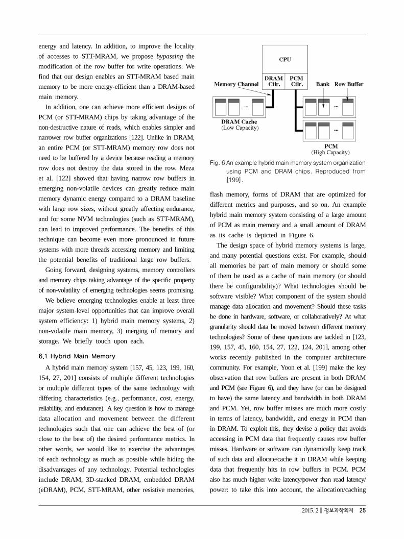
A hybrid main memory system [157, 45, 123, 199, 160, 154, 27, 201] consists of multiple different technologies or multiple different types of the same technology with differing characteristics (e.g., performance, cost, energy, reliability, and endurance). A key question is how to manage data allocation and movement between the different technologies such that one can achieve the best of (or close to the best of) the desired performance metrics. In other words, we would like to exercise the advantages of each technology as much as possible while hiding the disadvantages of any technology. Potential technologies include DRAM, 3D-stacked DRAM, embedded DRAM (eDRAM), PCM, STT-MRAM, other resistive memories,
Fig. 6 An example hybrid main memory system organization
using PCM and DRAM chips. Reproduced from
[199].
flash memory, forms of DRAM that are optimized for different metrics and purposes, and so on. An example hybrid main memory system consisting of a large amount of PCM as main memory and a small amount of DRAM as its cache is depicted in Figure 6.
The design space of hybrid memory systems is large, and many potential questions exist. For example, should all memories be part of main memory or should some of them be used as a cache of main memory (or should there be configurability)? What technologies should be software visible? What component of the system should manage data allocation and movement? Should these tasks be done in hardware, software, or collaboratively? At what granularity should data be moved between different memory technologies? Some of these questions are tackled in [123, 199, 157, 45, 160, 154, 27, 122, 124, 201], among other works recently published in the computer architecture community. For example, Yoon et al. [199] make the key observation that row buffers are present in both DRAM and PCM (see Figure 6), and they have (or can be designed to have) the same latency and bandwidth in both DRAM and PCM. Yet, row buffer misses are much more costly in terms of latency, bandwidth, and energy in PCM than in DRAM. To exploit this, they devise a policy that avoids accessing in PCM data that frequently causes row buffer misses. Hardware or software can dynamically keep track of such data and allocate/cache it in DRAM while keeping data that frequently hits in row buffers in PCM. PCM also has much higher write latency/power than read latency/ power: to take this into account, the allocation/caching
26 특집원고Ⅰ The Main Memory System: Challenges and Opportunities
policy is biased such that pages that are written to more likely stay in DRAM [199].
Other works have examined how to reduce the latency, energy, and cost of managing the metadata required to locate data in a large DRAM cache in hybrid main memories [116, 123]. Such metadata is typically stored in costly and high-energy SRAM in traditional CPU cache architectures. In a recent work, Meza et al. made the observation that only a small amount of data is accessed with high locality in a large DRAM cache and so only a small amount of metadata needs to be kept to locate data with locality in the cache. By distributing metadata within the DRAM cache itself (developed concurrently in [116]) and applying their technique, the authors show that similar performance to storing full cache metadata (which for large DRAM caches can be 10's or 100's of MB in size) can be achieved with smaller storage size.
Note that hybrid memory need not consist of completely different underlying technologies. A promising approach is to combine multiple different DRAM chips, optimized for different purposes. One recent work proposed the use of low-latency and high-latency DIMMs in separate memory channels and allocating performance-critical data to low-latency DIMMs to improve performance and energy- efficiency at the same time [27]. Another recent work examined the use of highly-reliable DIMMs (protected with ECC) and unreliable DIMMs in separate memory channels and allocating error-vulnerable data to highly-reliable DIMMs [119]. The authors observed that for certain data-intensive server workloads, data can be classified into different categories based on how sensitive (or insensitive) they are to errors. They show that by placing a small amount of error-sensitive data in more expensive ECC memory and the rest of data in less expensive non-ECC memory, their technique can help maximize server availability while minimizing server memory cost [119]. We believe these approaches are quite promising for scaling the DRAM technology into the future by specializing DRAM chips for different purposes. These approaches that exploit heterogeneity do increase system complexity but that complexity may be warranted if it is lower than the complexity of scaling DRAM chips using the same optimization techniques the DRAM industry has been using so far.
6.2 Making NVM Reliable and Secure
In contrast to traditional persistent storage devices, which operate on large blocks of data (hundreds or thousands of bits), new non-volatile memory devices provide the opportunity to operate on data at a much smaller granularity (several or tens of bits). Such operation can greatly simplify the implementation of higher-level atomicity and consistency guarantees by allowing software to obtain exclusive access to and perform more fine-grained updates on persistent data. Past works have shown that this behavior of NVM devices can be exploited to improve system reliability with new file system designs [36], improve system performance and reliability with better checkpointing approaches [46], and design more energy-efficient and higher performance system architecture abstractions for storage and memory [124].
On the flip side, the same non-volatility can lead to potentially unforeseen security and privacy issues that do not exist for existing DRAM main memories: critical and private data (e.g., unencrypted passwords stored in system memory) can persist long after the system is powered down [30], and an attacker can take advantage of this fact. To help combat this issue, some recent works have examined efficient encryption/decryption schemes for PCM devices [95]. Wearout issues of emerging technology can also cause attacks that can intentionally degrade memory capacity in the system (e.g., an attacker can devise adversarial access patterns that repeatedly write to the same physical locations in an attempt to rapidly wear out a device), and several works have examined ways to detect (and mitigate the effects of) such access patterns [156, 169]. Securing non-volatile main memory is therefore an important systems challenge.
6.3 Merging of Memory and Storage
One promising opportunity fast, byte-addressable, non- volatile emerging memory technologies open up is the design of a system and applications that can manipulate persistent data directly in memory instead of going through a slow storage interface. This can enable not only much more efficient systems but also new and more robust applications. We discuss this opportunity in more detail below.
Traditional computer systems have a two-level storage model: they access and manipulate 1) volatile data in main
2015. 2 정보과학회지 27
memory (DRAM, today) with a fast load/store interface, 2) persistent data in storage media (flash and hard disks, today) with a slower file system interface. Unfortunately, such a decoupled memory/storage model managed via vastly different techniques (fast, hardware-accelerated memory management units on one hand, and slow operating/file system (OS/FS) software on the other) suffers from large inefficiencies in locating data, moving data, and translating data between the different formats of these two levels of storage that are accessed via two vastly different interfaces, leading to potentially large amounts of wasted work and energy [124, 168]. The two different interfaces arose largely due to the large discrepancy in the access latencies of conventional technologies used to construct volatile memory (DRAM) and persistent storage (hard disks and flash memory).
Today, new non-volatile memory technologies, e.g, PCM, STT-MRAM, RRAM, show the promise of storage capacity and endurance similar to or better than flash memory at latencies comparable to DRAM. This makes them prime candidates for providing applications a persistent single- level store with a single load/store-like interface to access all system data (including volatile and persistent data), and several recent works have examined various abstractions to help unify storage and memory (e.g., [189, 34, 144, 124]).
In fact, if we keep the traditional two-level memory/ storage model in the presence of these fast NVM devices as part of storage, the operating system and file system code for locating, moving, and translating persistent data from the non-volatile NVM devices to volatile DRAM for manipulation purposes becomes a great bottleneck, causing most of the memory energy consumption and degrading performance by an order of magnitude in some data-intensive workloads, as we showed in recent work [124]. With energy as a key constraint, and in light of modern high-density NVM devices, a promising research direction is to unify and coordinate the management of volatile memory and persistent storage in a single level, to eliminate wasted energy and performance, and to simplify the programming model at the same time.
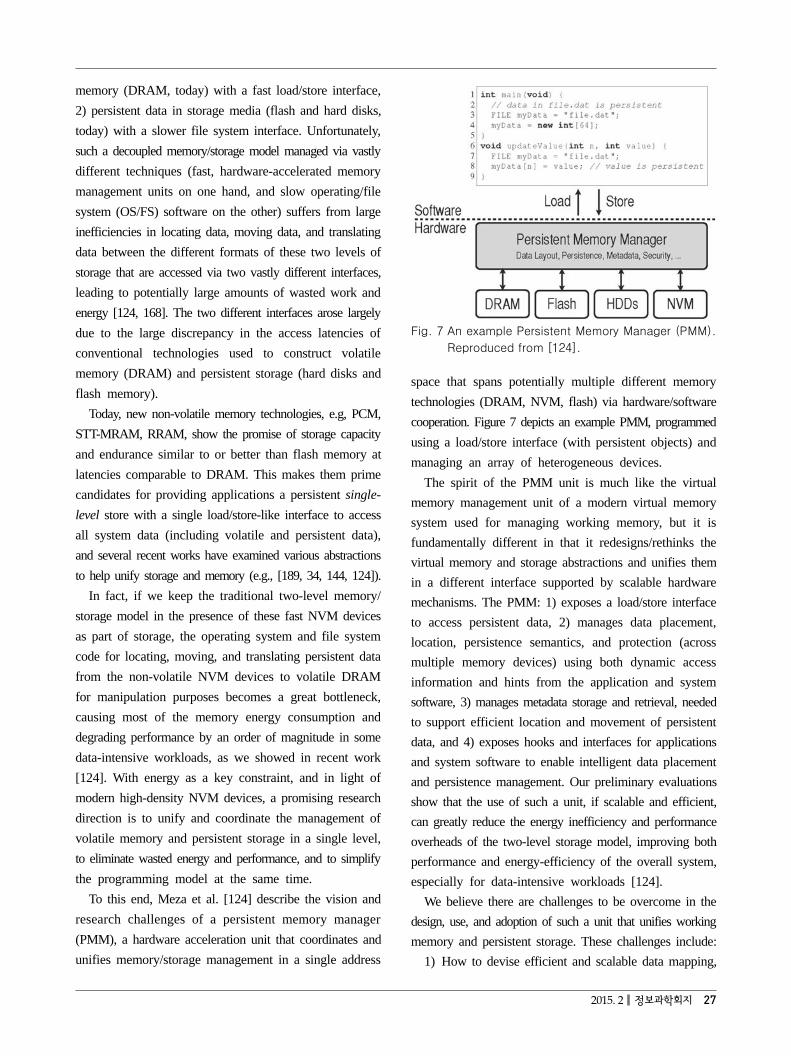
To this end, Meza et al. [124] describe the vision and research challenges of a persistent memory manager (PMM), a hardware acceleration unit that coordinates and unifies memory/storage management in a single address
Fig. 7 An example Persistent Memory Manager (PMM).
Reproduced from [124].
space that spans potentially multiple different memory technologies (DRAM, NVM, flash) via hardware/software cooperation. Figure 7 depicts an example PMM, programmed using a load/store interface (with persistent objects) and managing an array of heterogeneous devices.
The spirit of the PMM unit is much like the virtual memory management unit of a modern virtual memory system used for managing working memory, but it is fundamentally different in that it redesigns/rethinks the virtual memory and storage abstractions and unifies them in a different interface supported by scalable hardware mechanisms. The PMM: 1) exposes a load/store interface to access persistent data, 2) manages data placement, location, persistence semantics, and protection (across multiple memory devices) using both dynamic access information and hints from the application and system software, 3) manages metadata storage and retrieval, needed to support efficient location and movement of persistent data, and 4) exposes hooks and interfaces for applications and system software to enable intelligent data placement and persistence management. Our preliminary evaluations show that the use of such a unit, if scalable and efficient, can greatly reduce the energy inefficiency and performance overheads of the two-level storage model, improving both performance and energy-efficiency of the overall system, especially for data-intensive workloads [124].
We believe there are challenges to be overcome in the design, use, and adoption of such a unit that unifies working memory and persistent storage. These challenges include:
1) How to devise efficient and scalable data mapping,
28 특집원고Ⅰ The Main Memory System: Challenges and Opportunities
placement, and location mechanisms (which likely need to be hardware/software cooperative).
2) How to ensure that the consistency and protection requirements of different types of data are adequately, correctly, and reliably satisfied (One example recent work tackled the problem of providing storage consistency at high performance [118]). How to enable the reliable and effective coexistence and manipulation of volatile and persistent data.
3) How to redesign applications such that they can take advantage of the unified memory/storage interface and make the best use of it by providing appropriate hints for data allocation and placement to the persistent memory manager.
4) How to provide efficient and high-performance backward compatibility mechanisms for enabling and enhancing existing memory and storage interfaces in a single- level store. These techniques can seamlessly enable applications targeting traditional two-level storage systems to take advantage of the performance and energy-efficiency benefits of systems employing single-level stores. We believe such techniques are needed to ease the software transition to a radically different storage interface.
5) How to design system resources such that they can concurrently handle applications/access-patterns that manipulate persistent data as well as those that manipulate non-persistent data. (One example recent work [202] tackled the problem of designing effective memory scheduling policies in the presence of these two different types of applications/access-patterns.)
7. New Research Challenge 3:Predictable Performance
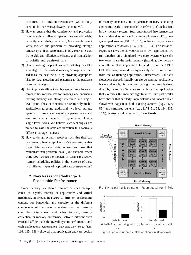
Since memory is a shared resource between multiple cores (or, agents, threads, or applications and virtual machines), as shown in Figure 8, different applications contend for bandwidth and capacity at the different components of the memory system, such as memory controllers, interconnects and caches. As such, memory contention, or memory interference, between different cores critically affects both the overall system performance and each application's performance. Our past work (e.g., [126, 134, 135, 139]) showed that application-unaware design
of memory controllers, and in particular, memory scheduling algorithms, leads to uncontrolled interference of applications in the memory system. Such uncontrolled interference can lead to denial of service to some applications [126], low system performance [134, 135, 139], unfair and unpredictable application slowdowns [134, 174, 51, 54]. For instance, Figure 9 shows the slowdowns when two applications are run together on a simulated two-core system where the two cores share the main memory (including the memory controllers). The application leslie3d (from the SPEC CPU2006 suite) slows down significantly due to interference from the co-running application. Furthermore, leslie3d's slowdown depends heavily on the co-running application. It slows down by 2x when run with gcc, whereas it slows down by more than 5x when run with mcf, an application that exercises the memory significantly. Our past works have shown that similarly unpredictable and uncontrollable slowdowns happen in both existing systems (e.g., [126, 85]) and simulated systems (e.g., [174, 51, 54, 134, 135, 139]), across a wide variety of workloads.
Fig. 8 A typical multicore system. Reproduced from [130].
(a) leslie3d co-running with
gcc
(b) leslie3d co-running with
mcf
Fig. 9 High and unpredictable application slowdowns
2015. 2 정보과학회지 29
Building QoS and application awareness into the different components of the memory system such as memory controllers, caches, interconnects is important to control interference at these different components and mitigate/ eliminate unfairness and unpredictability. Towards this end, previous works have explored two different solution directions: 1) to mitigate interference, thereby reducing application slowdowns and improving overall system performance, 2) to precisely quantify and control the impact of interference on application slowdowns, thereby providing performance guarantees to applications that need such guarantees. We discuss these two different approaches and associated research problems next.
7.1 Mitigating Interference
In order to mitigate interference at the different components of memory system, two kinds of approaches have been explored. The resources could be either smart (i.e., aware of threads' or applications' interference in memory) or dumb (i.e., unaware of threads' or applications' interference in memory) as we describe below.2)
7.1.1 Smart Resources
The smart resources approach equips resources (such as memory controllers, interconnects and caches) with the intelligence to 1) be aware of interference characteristics between applications and 2) prevent unfair application slowdowns and performance degradation. Several of our past works have taken the smart resources approach and designed QoS-aware memory controllers [134, 135, 139, 127, 89, 90, 91, 9, 102, 52, 174, 85, 175] and interconnects [39, 40, 41, 64, 62, 25, 145, 146, 65, 125]. Our and other previous works have explored smart shared cache management policies that 1) allocate shared cache capacity to applications in a manner that is aware of their cache utility [159, 194], 2) modify the cache replacement and insertion policies to be aware of the data reuse and memory access behavior of applications [158, 73, 72, 164, 84, 167]. All these QoS-aware schemes enable resources (such as memory controllers, interconnects and caches) to detect interference between applications by means of monitoring their access characteristics and allocate resources such as
2) For the rest of this article, without loss of generality, we use the term thread and application interchangeably. From the point of view of a smart resource, the resource needs to becommunicated at least the hardware context identifier of the application/thread that is generating requests to be serviced.
memory bandwidth, interconnect link bandwidth and cache capacity to applications such that interference between applications is mitigated.
We provide some brief examples of the smart resources approach by focusing on QoS-aware memory controllers [134, 135, 139, 127, 89, 90, 91, 9, 102, 52, 174, 85, 175].
Mutlu and Moscibroda [135, 139] show that uncontrolled inter-thread interference in the memory controller can destroy the memory-level parallelism (MLP) [61, 148, 140, 32, 137, 138, 49, 141] and serialize requests of individual threads, leading to significant degradation in both single-thread and system performance in multi-core/ multi-threaded systems. Hence, many techniques devised to parallelize a thread's memory requests to tolerate memory latency by exploiting MLP, such as out-of-order execution [183, 149, 150], non-blocking caches [96], runahead execution [49, 140, 32, 137, 136, 138, 141, 28, 133] and other techniques [31, 203, 158], can become ineffective if the memory controller is not aware of threads. They propose PAR-BS, a memory scheduler that forms a rank order among threads and services threads in that order, to tackle the interference problem and improve performance and fairness.
Kim et al. [89] observe that applications that have received the least service from the memory controllers in the past, would benefit from quick request service (in the future). They propose ATLAS [89], a QoS-aware memory controller design that monitors and ranks applications based on the amount of service each application receives at the memory controllers and prioritizes requests of applications with low attained memory service. Kim et al. [90, 91], in a later work, observe that prioritizing between all applications solely based on one access characteristic, e.g., the attained memory service in ATLAS, could unfairly slow down very memory-intensive applications. To solve this problem, they propose the thread cluster memory scheduler (TCM) [90, 91], which employs heterogeneous request scheduling policies for different types of applications. TCM classifies applications into two clusters, the latency-sensitive and bandwidth-sensitive clusters, prioritizes the latency-sensitive cluster, and employs a different policy to rank and prioritize among applications within each cluster, with the goal of optimizing for both performance and fairness. Results show that TCM can achieve both high performance and fairness compared to the best schedulers of the time.
30 특집원고Ⅰ The Main Memory System: Challenges and Opportunities
Most recently, Subramanian et al. [175] propose the blacklisting memory scheduler (BLISS) based on the observation that it is not necessary to employ a full ordered ranking across all applications, like ATLAS and TCM do, due to two key reasons - high hardware complexity and unfair application slowdowns from prioritizing some high-memory-intensity applications over other high-memory- intensity applications. Hence, they propose to separate applications into only two groups, one containing interference- causing applications and the other containing vulnerable-to- interference applications and prioritize the vulnerable-to- interference group over the interference-causing group. Such a scheme not only greatly reduces the hardware complexity and critical path latency of the memory scheduler, but also prevents applications from slowing down unfairly, thereby improving system performance.
Besides interference between requests of different threads, other sources of interference such as interference in the memory controller among threads of the same application [176, 179, 75, 76, 177, 178, 48, 12, 16] and interference caused by prefetch requests to demand requests [172, 181, 66, 102, 104, 105, 55, 56, 53, 167, 142] are also important problems to tackle and they offer ample scope for further research.
A challenge with the smart resources approach is the coordination of resource allocation decisions across different resources, such as main memory, interconnects and shared caches. To provide QoS across the entire system, the actions of different resources need to be coordinated. Several works examined such coordination mechanisms. One example of such a scheme is a coordinated resource management scheme proposed by Bitirgen et al. [13] that employs machine learning to predict each application's performance for different possible resource allocations. Resources are then allocated appropriately to different applications such that a global system performance metric is optimized. Another example of such a scheme is a recent work by Wang and Martinez [190] that employs a market- dynamics-inspired mechanism to coordinate allocation decisions across resources. Approaches to coordinate resource allocation and scheduling decisions across multiple resources in the memory system, whether they use machine learning, game theory, or feedback based control, are a promising research topic that offers ample scope for future exploration.
7.1.2 Dumb Resources
The dumb resources approach, rather than modifying the resources themselves to be QoS- and application-aware, controls the resources and their allocation at different points in the system (e.g., at the cores/sources or at the system software) such that unfair slowdowns and performance degradation are mitigated. For instance, Ebrahimi et al. propose Fairness via Source Throttling (FST) [51, 54, 53], which throttles applications at the source (processor core) to regulate the number of requests that are sent to the shared caches and main memory from the processor core. Kayiran et al. [82] throttle the thread-level parallelism of the GPU to mitigate memory contention related slowdowns in heterogeneous architectures consisting of both CPUs and GPUs. Das et al. [38] propose to map applications to cores (by modifying the application scheduler in the operating system) in a manner that is aware of the applications' interconnect and memory access characteristics. Muralidhara et al. [128] propose to partition memory channels among applications such the data of applications that interfere significantly with each other are mapped to different memory channels. Other works [74, 113, 193, 85] build upon [128] and partition banks between applications at a fine-grained level to prevent different applications' request streams from interfering at the same banks. Zhuravlev et al. [204] and Tang et al. [180] propose to mitigate interference by co-scheduling threads that interact well and interfere less at the shared resources. Kaseridis et al. [81] propose to interleave data across channels and banks such that threads benefit from locality in the DRAM row-buffer, while not causing significant interference to each other. On the interconnect side, there has been a growing body of work on source throttling mechanisms [145, 146, 25, 59, 182, 63, 10] that detect congestion or slowdowns within the network and throttle the injection rates of applications in an application-aware manner to maximize both system performance and fairness.
One common characteristic among all these dumb resources approaches is that they regulate the amount of contention at the caches, interconnects and main memory by controlling their operation/allocation from a different agent such as the cores or the operating system, while not modifying the resources themselves to be QoS- or application-aware. This has the advantage of keeping the
2015. 2 정보과학회지 31
resources themselves simple, while also potentially enabling better coordination of allocation decisions across multiple resources. On the other hand, the disadvantages of the dumb resources approach are that 1) each resource may not be best utilized to provide the highest performance because it cannot make interference-aware decisions, 2) monitoring and control mechanisms to understand and decide how to best control operation/allocation from a different agent than the resources themselves to achieve a particular goal may increase complexity.
7.1.3 Integrated Approaches to QoS and Resource
Management
Even though both the smart resources and dumb resources approaches can greatly mitigate interference and provide QoS in the memory system when employed individually, they each have advantages and disadvantages that are unique, as we discussed above. Therefore, integrating the smart resources and dumb resources approaches can enable better interference mitigation than employing either approach alone by exploiting the advantages of each approach. An early example of such an integrated resource management approach is the Integrated Memory Partitioning and Scheduling (IMPS) scheme [128], which combines memory channel partitioning in the operating system (a dumb resource approach) along with simple application- aware memory request scheduling in the memory controller (a smart resource approach), leading to higher performance than when either approach is employed alone. Combining different approaches to memory QoS and resource management, both smart and dumb, with the goal of more effective interference mitigation is therefore a promising area for future research and exploration.
7.2 Quantifying and Controlling Interference
While several previous works have focused on mitigating interference at the different components of a memory system, with the goals of improving performance and preventing unfair application slowdowns, few previous works have focused on precisely quantifying and controlling the impact of interference on application slowdowns, with the goal of providing soft or hard performance guarantees. An application's susceptibility to interference and, consequently, its performance, depends on which other applications it is sharing resources with: an application
can sometimes have very high performance and at other times very low performance on the same system, solely depending on its co-runners (as we have shown in an example in Figure 9). A critical research challenge is therefore how to design the memory system (including all shared resources such as main memory, caches, and interconnects) such that 1) the performance of each application is predictable and controllable, and performance requirements of each application are satisfied, while 2) the performance and efficiency of the entire system are as high as needed or possible.
A promising solution direction to address this predictable performance challenge is to devise mechanisms that are effective and accurate at 1) estimating and predicting application performance in the presence of inter-application interference in a dynamic system with continuously incoming and outgoing applications, and 2) enforcing end-to-end performance guarantees within the entire shared memory system. We discuss briefly several prior works that took some of the first steps to achieve these goals and conclude with some promising future directions to pursue.
Stall Time Fair Memory Scheduling (STFM) [134] is one of the first works on estimating the impact of inter-application memory interference on performance. STFM estimates the impact of memory interference at the main memory alone on application slowdowns. It does so by estimating the impact of delaying every individual request of an application on its slowdown. Fairness via Source Throttling (FST) [51, 54] and Per-Thread Cycle Accounting [47] employ a scheme similar to STFM to estimate the impact of main memory interference, while also taking into account interference at the shared caches. While these approaches are good starting points towards addressing the challenge of estimating and predicting application slowdowns in the presence of memory interference, our recent work [174] observed that the slowdown estimates from STFM, FST and Per-Thread Cycle Accounting are relatively inaccurate since they estimate interference at an individual request granularity.
We have recently designed a simple method, called MISE (Memory-interference Induced Slowdown Estimation) [174], for estimating application slowdowns accurately in
32 특집원고Ⅰ The Main Memory System: Challenges and Opportunities
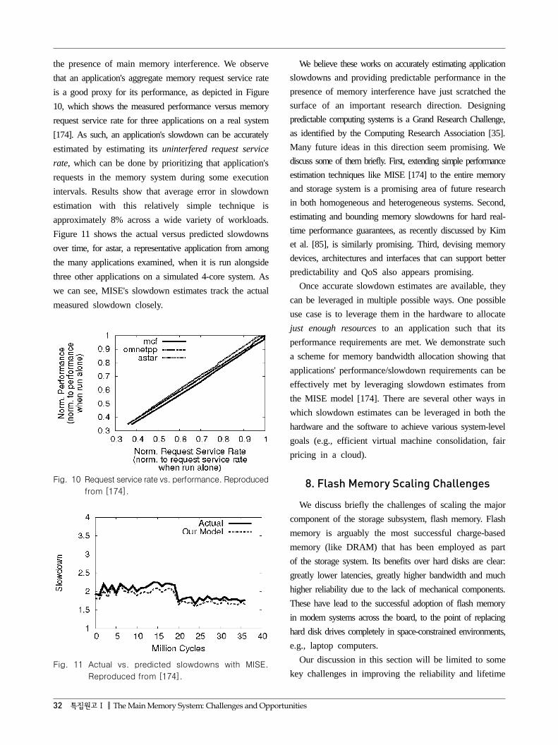
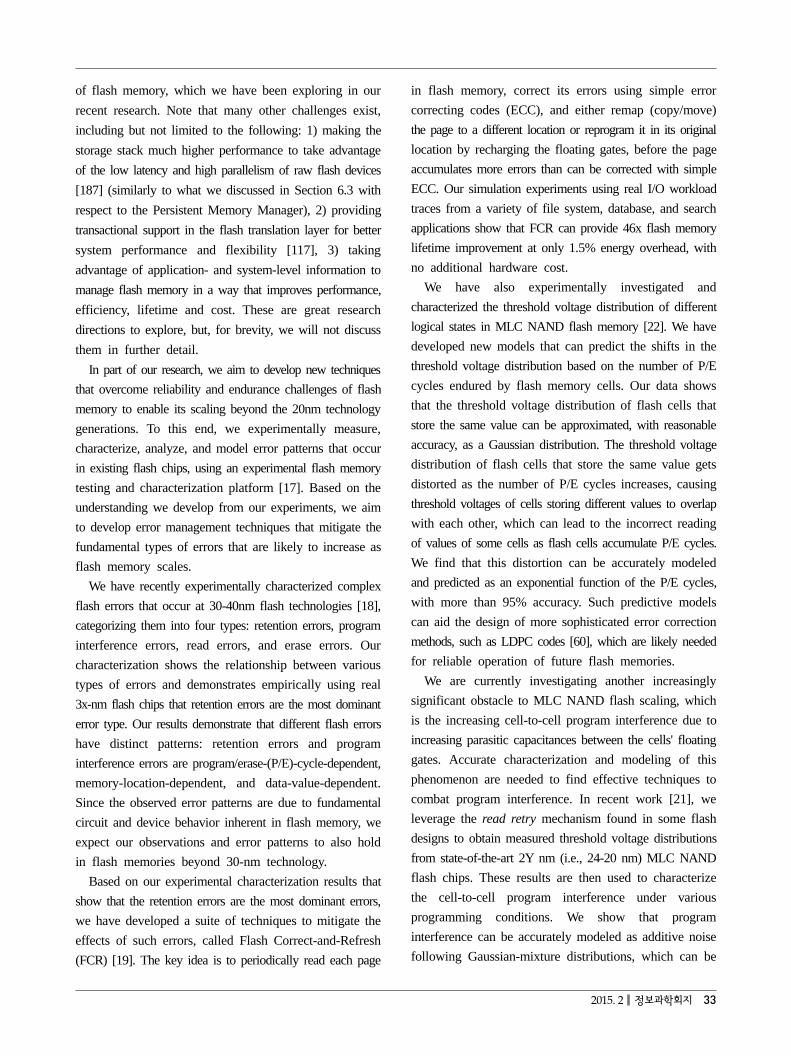
the presence of main memory interference. We observe that an application's aggregate memory request service rate is a good proxy for its performance, as depicted in Figure 10, which shows the measured performance versus memory request service rate for three applications on a real system [174]. As such, an application's slowdown can be accurately estimated by estimating its uninterfered request service rate, which can be done by prioritizing that application's requests in the memory system during some execution intervals. Results show that average error in slowdown estimation with this relatively simple technique is approximately 8% across a wide variety of workloads. Figure 11 shows the actual versus predicted slowdowns over time, for astar, a representative application from among the many applications examined, when it is run alongside three other applications on a simulated 4-core system. As we can see, MISE's slowdown estimates track the actual measured slowdown closely.
Fig. 10 Request service rate vs. performance. Reproduced
from [174].
Fig. 11 Actual vs. predicted slowdowns with MISE.
Reproduced from [174].
We believe these works on accurately estimating application slowdowns and providing predictable performance in the presence of memory interference have just scratched the surface of an important research direction. Designing predictable computing systems is a Grand Research Challenge, as identified by the Computing Research Association [35]. Many future ideas in this direction seem promising. We discuss some of them briefly. First, extending simple performance estimation techniques like MISE [174] to the entire memory and storage system is a promising area of future research in both homogeneous and heterogeneous systems. Second, estimating and bounding memory slowdowns for hard real- time performance guarantees, as recently discussed by Kim et al. [85], is similarly promising. Third, devising memory devices, architectures and interfaces that can support better predictability and QoS also appears promising.
Once accurate slowdown estimates are available, they can be leveraged in multiple possible ways. One possible use case is to leverage them in the hardware to allocate just enough resources to an application such that its performance requirements are met. We demonstrate such a scheme for memory bandwidth allocation showing that applications' performance/slowdown requirements can be effectively met by leveraging slowdown estimates from the MISE model [174]. There are several other ways in which slowdown estimates can be leveraged in both the hardware and the software to achieve various system-level goals (e.g., efficient virtual machine consolidation, fair pricing in a cloud).
8. Flash Memory Scaling Challenges
We discuss briefly the challenges of scaling the major component of the storage subsystem, flash memory. Flash memory is arguably the most successful charge-based memory (like DRAM) that has been employed as part of the storage system. Its benefits over hard disks are clear: greatly lower latencies, greatly higher bandwidth and much higher reliability due to the lack of mechanical components. These have lead to the successful adoption of flash memory in modern systems across the board, to the point of replacing hard disk drives completely in space-constrained environments, e.g., laptop computers.
Our discussion in this section will be limited to some key challenges in improving the reliability and lifetime
2015. 2 정보과학회지 33
of flash memory, which we have been exploring in our recent research. Note that many other challenges exist, including but not limited to the following: 1) making the storage stack much higher performance to take advantage of the low latency and high parallelism of raw flash devices [187] (similarly to what we discussed in Section 6.3 with respect to the Persistent Memory Manager), 2) providing transactional support in the flash translation layer for better system performance and flexibility [117], 3) taking advantage of application- and system-level information to manage flash memory in a way that improves performance, efficiency, lifetime and cost. These are great research directions to explore, but, for brevity, we will not discuss them in further detail.
In part of our research, we aim to develop new techniques that overcome reliability and endurance challenges of flash memory to enable its scaling beyond the 20nm technology generations. To this end, we experimentally measure, characterize, analyze, and model error patterns that occur in existing flash chips, using an experimental flash memory testing and characterization platform [17]. Based on the understanding we develop from our experiments, we aim to develop error management techniques that mitigate the fundamental types of errors that are likely to increase as flash memory scales.
We have recently experimentally characterized complex flash errors that occur at 30-40nm flash technologies [18], categorizing them into four types: retention errors, program interference errors, read errors, and erase errors. Our characterization shows the relationship between various types of errors and demonstrates empirically using real 3x-nm flash chips that retention errors are the most dominant error type. Our results demonstrate that different flash errors have distinct patterns: retention errors and program interference errors are program/erase-(P/E)-cycle-dependent, memory-location-dependent, and data-value-dependent. Since the observed error patterns are due to fundamental circuit and device behavior inherent in flash memory, we expect our observations and error patterns to also hold in flash memories beyond 30-nm technology.
Based on our experimental characterization results that show that the retention errors are the most dominant errors, we have developed a suite of techniques to mitigate the effects of such errors, called Flash Correct-and-Refresh (FCR) [19]. The key idea is to periodically read each page
in flash memory, correct its errors using simple error correcting codes (ECC), and either remap (copy/move) the page to a different location or reprogram it in its original location by recharging the floating gates, before the page accumulates more errors than can be corrected with simple ECC. Our simulation experiments using real I/O workload traces from a variety of file system, database, and search applications show that FCR can provide 46x flash memory lifetime improvement at only 1.5% energy overhead, with no additional hardware cost.
We have also experimentally investigated and characterized the threshold voltage distribution of different logical states in MLC NAND flash memory [22]. We have developed new models that can predict the shifts in the threshold voltage distribution based on the number of P/E cycles endured by flash memory cells. Our data shows that the threshold voltage distribution of flash cells that store the same value can be approximated, with reasonable accuracy, as a Gaussian distribution. The threshold voltage distribution of flash cells that store the same value gets distorted as the number of P/E cycles increases, causing threshold voltages of cells storing different values to overlap with each other, which can lead to the incorrect reading of values of some cells as flash cells accumulate P/E cycles. We find that this distortion can be accurately modeled and predicted as an exponential function of the P/E cycles, with more than 95% accuracy. Such predictive models can aid the design of more sophisticated error correction methods, such as LDPC codes [60], which are likely needed for reliable operation of future flash memories.
We are currently investigating another increasingly significant obstacle to MLC NAND flash scaling, which is the increasing cell-to-cell program interference due to increasing parasitic capacitances between the cells' floating gates. Accurate characterization and modeling of this phenomenon are needed to find effective techniques to combat program interference. In recent work [21], we leverage the read retry mechanism found in some flash designs to obtain measured threshold voltage distributions from state-of-the-art 2Y nm (i.e., 24-20 nm) MLC NAND flash chips. These results are then used to characterize the cell-to-cell program interference under various programming conditions. We show that program interference can be accurately modeled as additive noise following Gaussian-mixture distributions, which can be
34 특집원고Ⅰ The Main Memory System: Challenges and Opportunities
predicted with 96.8% accuracy using linear regression models. We use these models to develop and evaluate a read reference voltage prediction technique that reduces the raw flash bit error rate by 64% and increases the flash lifetime by 30%. More detail can be found in Cai et al. [21].
To improve flash memory lifetime, we have developed a mechanism called Neighbor-Cell Assisted Correction (NAC) [23], which uses the value information of cells in a neighboring page to correct errors found on a page when reading. This mechanism takes advantage of the new empirical observation that identifying the value stored in the immediate-neighbor cell makes it easier to determine the data value stored in the cell that is being read. The key idea is to re-read a flash memory page that fails error correction codes (ECC) with the set of read reference voltage values corresponding to the conditional threshold voltage distribution assuming a neighbor cell value and use the re-read values to correct the cells that have neighbors with that value. Our simulations show that NAC effectively improves flash memory lifetime by 33% while having no (at nominal lifetime) or very modest (less than 5% at extended lifetime) performance overhead.
Most recently, we have provided a rigorous characterization of retention errors in NAND flash memory devices and new techniques to take advantage of this characterization to improve flash memory lifetime [24]. We have extensively characterized how the threshold voltage distribution of flash memory changes under different retention age, i.e., the length of time since a flash cell is programmed. We observe from our characterization results that 1) the optimal read reference voltage of a flash cell, at which the data can be read with the lowest raw bit error rate, systematically changes with the cell's retention age and 2) different regions of flash memory can have different retention ages, and hence different optimal read reference voltages. Based on these observations, we propose a new technique to learn and apply the optimal read reference voltage online (called Retention Optimized Reading). Our evaluations show that our technique can extend flash memory lifetime by 64% and reduce average error correction latency by 7% with only a 768 KB storage overhead in flash memory for a 512 GB flash-based SSD. We also propose a technique to recover data with uncorrectable errors by identifying and probabilistically correcting flash cells with retention errors. Our evaluation shows that this technique can
effectively recover data from uncorrectable flash errors and reduce Raw Bit Error Rate (RBER) by 50%. More detail can be found in Cai et al. [24].
These works, to our knowledge, are the first open- literature works that 1) characterize various aspects of real state-of-the-art flash memory chips, focusing on reliability and scaling challenges, and 2) exploit the insights developed from these characterizations to develop new mechanisms that can improve flash memory reliability and lifetime. We believe such an experimental- and characterization- based approach (which we also employ for DRAM [112, 83, 93, 107], as we discussed in Section 5) to developing novel techniques for both existing and emerging memory technologies is critically important as it 1) provides a solid basis (i.e., real data from modern devices) on which future analyses and new techniques can be based, 2) reveals new scaling trends in modern devices, pointing to important challenges in the field, and 3) equips the research community with reliable models and analyses that can be openly used to innovate in areas where experimental information is usually scarce in the open literature due to heavy competition within industry, thereby enhancing research and investigation in areas that are previously deemed to be difficult to research.
Going forward, we believe more accurate and detailed characterization of flash memory error mechanisms are needed to devise models that can aid the design of even more efficient and effective mechanisms to tolerate errors found in sub-20nm flash memories. A promising direction is the design of predictive models that the system (e.g., the flash controller or system software) can use to proactively estimate the occurrence of errors and take action to prevent the error before it happens. Flash-correct- and-refresh [19], read reference voltage prediction [21], and retention optimizated reading [24] mechanisms, described earlier, are early forms of such predictive error tolerance mechanisms. Methods for exploiting application and memory access characteristics to optimize flash performance, energy, lifetime and cost are also very promising to explore. We believe there is a bright future ahead for more aggressive and effective application- and data-characteristic-aware management mechanisms for flash memory (just like for DRAM and emerging memory technologies). Such techniques will likely aid effective scaling of flash memory technology into the future.
2015. 2 정보과학회지 35
9. Conclusion
We have described several research directions and ideas to enhance memory scaling via system and architecture- level approaches. We believe there are three key fundamental principles that are essential for memory scaling: 1) better cooperation between devices, system, and software, i.e., the efficient exposure of richer information up and down the layers of the system stack with the development of more flexible yet abstract interfaces that can scale well into the future, 2) better-than-worst-case design, i.e., design of the memory system such that it is optimized for the common case instead of the worst case, 3) heterogeneity in design, i.e., the use of heterogeneity at all levels in memory system design to enable the optimization of multiple metrics at the same time. We believe these three principles are related and sometimes coupled. For example, to exploit heterogeneity in the memory system, we may need to enable better cooperation between the devices and the system, e.g., as in the case of heterogeneous DRAM refresh rates [111], tiered-latency DRAM [106], heterogeneous- reliability memory [119], locality-aware management of hybrid memory systems [199] and the persistent memory manager for a heterogeneous array of memory/storage devices [124], five of the many ideas we have discussed in this paper.
We have shown that a promising approach to designing scalable memory systems is the co-design of memory and other system components to enable better system optimization. Enabling better cooperation across multiple levels of the computing stack, including software, microarchitecture, and devices can help scale the memory system by exposing more of the memory device characteristics to higher levels of the system stack such that the latter can tolerate and exploit such characteristics. Finally, heterogeneity in the design of the memory system can help overcome the memory scaling challenges at the device level by enabling better specialization of the memory system and its dynamic adaptation to different demands of various applications. We believe such system-level and integrated approaches will become increasingly important and effective as the underlying memory technology nears its scaling limits at the physical level and envision a near future full of innovation in main memory architecture, enabled by the co-design of the system and main memory.
Acknowledgments
The source code and data sets of some of the works we have discussed or alluded to (e.g., [164, 151, 93, 83, 195, 7, 108]) are available under open source software license at our research group, SAFARI's, tools website [1].
We would like to thank Rachata Ausavarungnirun for logistic help in preparing this article and earlier versions of it. Many thanks to all students in the SAFARI research group and collaborators at Carnegie Mellon as well as other universities, whom have contributed to the various works outlined in this article. Thanks also go to our research group's industrial sponsors over the past six years, including AMD, HP Labs, Huawei, IBM, Intel, Microsoft, Nvidia, Oracle, Qualcomm, Samsung. Some of the research reported here was also partially supported by GSRC, Intel URO Memory Hierarchy Program, Intel Science and Technology Center on Cloud Computing, NIH, NSF, and SRC. In particular, NSF grants 0953246, 1065112, 1147397, 1212962, 1320531, 1409723, 1423172 have supported parts of the research we have described.
This article is a significantly extended and revised version of an invited paper that appeared at the 5th International Memory Workshop [130], which was also presented at MemCon 2013 [131]. Part of the structure of this article is based on an evolving set of talks Onur Mutlu has delivered at various venues on Scaling the Memory System in the Many-Core Era and Rethinking Memory System Design for Data-Intensive Computing between 2010-2015, including invited talks at the 2011 International Symposium on Memory Management and ACM SIGPLAN Workshop on Memory System Performance and Correctness [132] and the 2012 DAC More Than Moore Technologies Workshop. Section 8 of this article is a significantly extended and revised version of the introduction of an invited article that appeared in a special issue of the Intel Technology Journal, titled Error Analysis and Retention-Aware Error Management for NAND Flash Memory [20].
References
[ 1 ] “SAFARI tools,” https://www.ece.cmu.edu/safari/tools.html.[ 2 ] “International technology roadmap for semiconductors
(ITRS),” 2011.[ 3 ] Hybrid Memory Consortium, 2012, http://www.
hybridmemorycube.org.
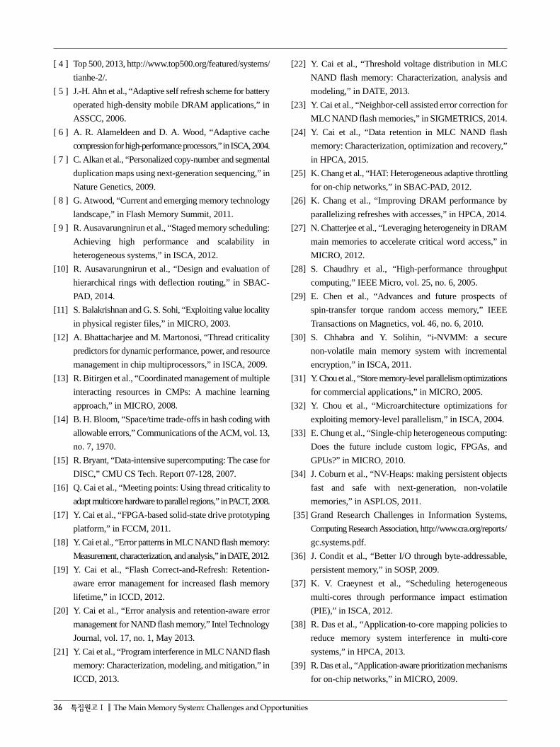
36 특집원고Ⅰ The Main Memory System: Challenges and Opportunities
[ 4 ] Top 500, 2013, http://www.top500.org/featured/systems/ tianhe-2/.
[ 5 ] J.-H. Ahn et al., “Adaptive self refresh scheme for battery operated high-density mobile DRAM applications,” in ASSCC, 2006.
[ 6 ] A. R. Alameldeen and D. A. Wood, “Adaptive cache compression for high-performance processors,” in ISCA, 2004.
[ 7 ] C. Alkan et al., “Personalized copy-number and segmental duplication maps using next-generation sequencing,” in Nature Genetics, 2009.
[ 8 ] G. Atwood, “Current and emerging memory technology landscape,” in Flash Memory Summit, 2011.
[ 9 ] R. Ausavarungnirun et al., “Staged memory scheduling: Achieving high performance and scalability in heterogeneous systems,” in ISCA, 2012.
[10] R. Ausavarungnirun et al., “Design and evaluation of hierarchical rings with deflection routing,” in SBAC- PAD, 2014.
[11] S. Balakrishnan and G. S. Sohi, “Exploiting value locality in physical register files,” in MICRO, 2003.
[12] A. Bhattacharjee and M. Martonosi, “Thread criticality predictors for dynamic performance, power, and resource management in chip multiprocessors,” in ISCA, 2009.
[13] R. Bitirgen et al., “Coordinated management of multiple interacting resources in CMPs: A machine learning approach,” in MICRO, 2008.
[14] B. H. Bloom, “Space/time trade-offs in hash coding with allowable errors,” Communications of the ACM, vol. 13, no. 7, 1970.
[15] R. Bryant, “Data-intensive supercomputing: The case for DISC,” CMU CS Tech. Report 07-128, 2007.
[16] Q. Cai et al., “Meeting points: Using thread criticality to adapt multicore hardware to parallel regions,” in PACT, 2008.
[17] Y. Cai et al., “FPGA-based solid-state drive prototyping platform,” in FCCM, 2011.
[18] Y. Cai et al., “Error patterns in MLC NAND flash memory: Measurement, characterization, and analysis,” in DATE, 2012.
[19] Y. Cai et al., “Flash Correct-and-Refresh: Retention- aware error management for increased flash memory lifetime,” in ICCD, 2012.
[20] Y. Cai et al., “Error analysis and retention-aware error management for NAND flash memory,” Intel Technology Journal, vol. 17, no. 1, May 2013.
[21] Y. Cai et al., “Program interference in MLC NAND flash memory: Characterization, modeling, and mitigation,” in ICCD, 2013.
[22] Y. Cai et al., “Threshold voltage distribution in MLC NAND flash memory: Characterization, analysis and modeling,” in DATE, 2013.
[23] Y. Cai et al., “Neighbor-cell assisted error correction for MLC NAND flash memories,” in SIGMETRICS, 2014.
[24] Y. Cai et al., “Data retention in MLC NAND flash memory: Characterization, optimization and recovery,” in HPCA, 2015.
[25] K. Chang et al., “HAT: Heterogeneous adaptive throttling for on-chip networks,” in SBAC-PAD, 2012.
[26] K. Chang et al., “Improving DRAM performance by parallelizing refreshes with accesses,” in HPCA, 2014.
[27] N. Chatterjee et al., “Leveraging heterogeneity in DRAM main memories to accelerate critical word access,” in MICRO, 2012.
[28] S. Chaudhry et al., “High-performance throughput computing,” IEEE Micro, vol. 25, no. 6, 2005.
[29] E. Chen et al., “Advances and future prospects of spin-transfer torque random access memory,” IEEE Transactions on Magnetics, vol. 46, no. 6, 2010.
[30] S. Chhabra and Y. Solihin, “i-NVMM: a secure non-volatile main memory system with incremental encryption,” in ISCA, 2011.
[31] Y. Chou et al., “Store memory-level parallelism optimizations for commercial applications,” in MICRO, 2005.
[32] Y. Chou et al., “Microarchitecture optimizations for exploiting memory-level parallelism,” in ISCA, 2004.
[33] E. Chung et al., “Single-chip heterogeneous computing: Does the future include custom logic, FPGAs, and GPUs?” in MICRO, 2010.
[34] J. Coburn et al., “NV-Heaps: making persistent objects fast and safe with next-generation, non-volatile memories,” in ASPLOS, 2011.
[35] Grand Research Challenges in Information Systems, Computing Research Association, http://www.cra.org/reports/ gc.systems.pdf.
[36] J. Condit et al., “Better I/O through byte-addressable, persistent memory,” in SOSP, 2009.
[37] K. V. Craeynest et al., “Scheduling heterogeneous multi-cores through performance impact estimation (PIE),” in ISCA, 2012.
[38] R. Das et al., “Application-to-core mapping policies to reduce memory system interference in multi-core systems,” in HPCA, 2013.
[39] R. Das et al., “Application-aware prioritization mechanisms for on-chip networks,” in MICRO, 2009.
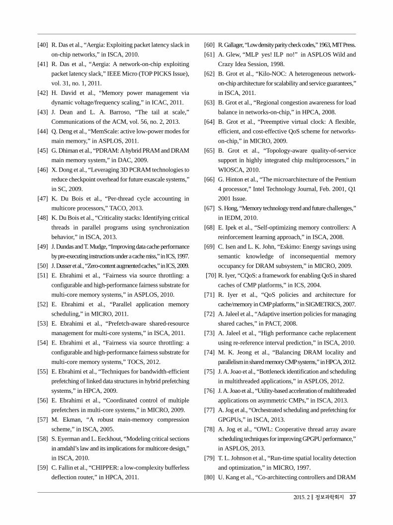
2015. 2 정보과학회지 37
[40] R. Das et al., “Aergia: Exploiting packet latency slack in on-chip networks,” in ISCA, 2010.
[41] R. Das et al., “Aergia: A network-on-chip exploiting packet latency slack,” IEEE Micro (TOP PICKS Issue), vol. 31, no. 1, 2011.
[42] H. David et al., “Memory power management via dynamic voltage/frequency scaling,” in ICAC, 2011.
[43] J. Dean and L. A. Barroso, “The tail at scale,” Communications of the ACM, vol. 56, no. 2, 2013.
[44] Q. Deng et al., “MemScale: active low-power modes for main memory,” in ASPLOS, 2011.
[45] G. Dhiman et al., “PDRAM: A hybrid PRAM and DRAM main memory system,” in DAC, 2009.
[46] X. Dong et al., “Leveraging 3D PCRAM technologies to reduce checkpoint overhead for future exascale systems,” in SC, 2009.
[47] K. Du Bois et al., “Per-thread cycle accounting in multicore processors,” TACO, 2013.
[48] K. Du Bois et al., “Criticality stacks: Identifying critical threads in parallel programs using synchronization behavior,” in ISCA, 2013.
[49] J. Dundas and T. Mudge, “Improving data cache performance by pre-executing instructions under a cache miss,” in ICS, 1997.
[50] J. Dusser et al., “Zero-content augmented caches,” in ICS, 2009.[51] E. Ebrahimi et al., “Fairness via source throttling: a
configurable and high-performance fairness substrate for multi-core memory systems,” in ASPLOS, 2010.
[52] E. Ebrahimi et al., “Parallel application memory scheduling,” in MICRO, 2011.
[53] E. Ebrahimi et al., “Prefetch-aware shared-resource management for multi-core systems,” in ISCA, 2011.
[54] E. Ebrahimi et al., “Fairness via source throttling: a configurable and high-performance fairness substrate for multi-core memory systems,” TOCS, 2012.
[55] E. Ebrahimi et al., “Techniques for bandwidth-efficient prefetching of linked data structures in hybrid prefetching systems,” in HPCA, 2009.
[56] E. Ebrahimi et al., “Coordinated control of multiple prefetchers in multi-core systems,” in MICRO, 2009.
[57] M. Ekman, “A robust main-memory compression scheme,” in ISCA, 2005.
[58] S. Eyerman and L. Eeckhout, “Modeling critical sections in amdahl’s law and its implications for multicore design,” in ISCA, 2010.
[59] C. Fallin et al., “CHIPPER: a low-complexity bufferless deflection router,” in HPCA, 2011.
[60] R. Gallager, “Low density parity check codes,” 1963, MIT Press.[61] A. Glew, “MLP yes! ILP no!” in ASPLOS Wild and
Crazy Idea Session, 1998.[62] B. Grot et al., “Kilo-NOC: A heterogeneous network-
on-chip architecture for scalability and service guarantees,” in ISCA, 2011.
[63] B. Grot et al., “Regional congestion awareness for load balance in networks-on-chip,” in HPCA, 2008.
[64] B. Grot et al., “Preemptive virtual clock: A flexible, efficient, and cost-effective QoS scheme for networks- on-chip,” in MICRO, 2009.
[65] B. Grot et al., “Topology-aware quality-of-service support in highly integrated chip multiprocessors,” in WIOSCA, 2010.
[66] G. Hinton et al., “The microarchitecture of the Pentium 4 processor,” Intel Technology Journal, Feb. 2001, Q1 2001 Issue.
[67] S. Hong, “Memory technology trend and future challenges,” in IEDM, 2010.
[68] E. Ipek et al., “Self-optimizing memory controllers: A reinforcement learning approach,” in ISCA, 2008.
[69] C. Isen and L. K. John, “Eskimo: Energy savings using semantic knowledge of inconsequential memory occupancy for DRAM subsystem,” in MICRO, 2009.
[70] R. Iyer, “CQoS: a framework for enabling QoS in shared caches of CMP platforms,” in ICS, 2004.
[71] R. Iyer et al., “QoS policies and architecture for cache/memory in CMP platforms,” in SIGMETRICS, 2007.
[72] A. Jaleel et al., “Adaptive insertion policies for managing shared caches,” in PACT, 2008.
[73] A. Jaleel et al., “High performance cache replacement using re-reference interval prediction,” in ISCA, 2010.
[74] M. K. Jeong et al., “Balancing DRAM locality and parallelism in shared memory CMP systems,” in HPCA, 2012.
[75] J. A. Joao et al., “Bottleneck identification and scheduling in multithreaded applications,” in ASPLOS, 2012.
[76] J. A. Joao et al., “Utility-based acceleration of multithreaded applications on asymmetric CMPs,” in ISCA, 2013.
[77] A. Jog et al., “Orchestrated scheduling and prefetching for GPGPUs,” in ISCA, 2013.
[78] A. Jog et al., “OWL: Cooperative thread array aware scheduling techniques for improving GPGPU performance,” in ASPLOS, 2013.
[79] T. L. Johnson et al., “Run-time spatial locality detection and optimization,” in MICRO, 1997.
[80] U. Kang et al., “Co-architecting controllers and DRAM
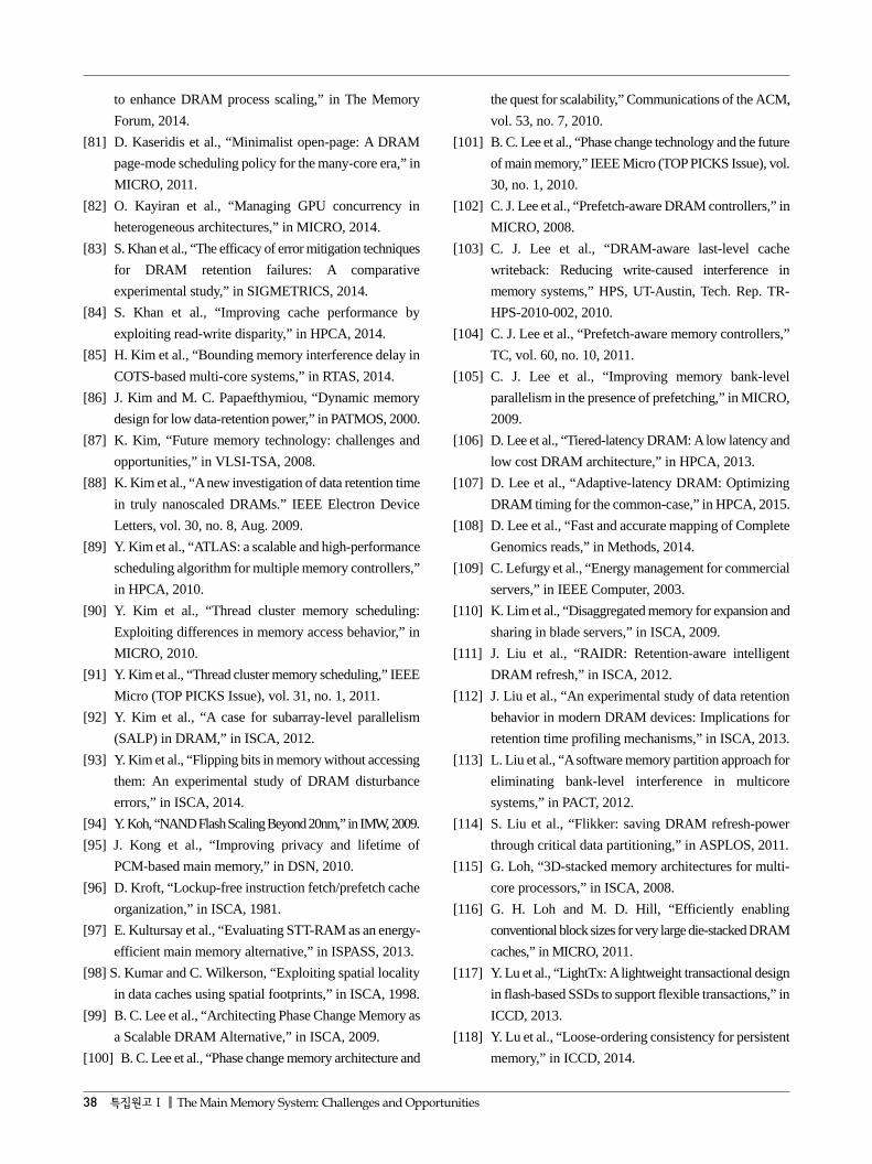
38 특집원고Ⅰ The Main Memory System: Challenges and Opportunities
to enhance DRAM process scaling,” in The Memory Forum, 2014.
[81] D. Kaseridis et al., “Minimalist open-page: A DRAM page-mode scheduling policy for the many-core era,” in MICRO, 2011.
[82] O. Kayiran et al., “Managing GPU concurrency in heterogeneous architectures,” in MICRO, 2014.
[83] S. Khan et al., “The efficacy of error mitigation techniques for DRAM retention failures: A comparative experimental study,” in SIGMETRICS, 2014.
[84] S. Khan et al., “Improving cache performance by exploiting read-write disparity,” in HPCA, 2014.
[85] H. Kim et al., “Bounding memory interference delay in COTS-based multi-core systems,” in RTAS, 2014.
[86] J. Kim and M. C. Papaefthymiou, “Dynamic memory design for low data-retention power,” in PATMOS, 2000.
[87] K. Kim, “Future memory technology: challenges and opportunities,” in VLSI-TSA, 2008.
[88] K. Kim et al., “A new investigation of data retention time in truly nanoscaled DRAMs.” IEEE Electron Device Letters, vol. 30, no. 8, Aug. 2009.
[89] Y. Kim et al., “ATLAS: a scalable and high-performance scheduling algorithm for multiple memory controllers,” in HPCA, 2010.
[90] Y. Kim et al., “Thread cluster memory scheduling: Exploiting differences in memory access behavior,” in MICRO, 2010.
[91] Y. Kim et al., “Thread cluster memory scheduling,” IEEE Micro (TOP PICKS Issue), vol. 31, no. 1, 2011.
[92] Y. Kim et al., “A case for subarray-level parallelism (SALP) in DRAM,” in ISCA, 2012.
[93] Y. Kim et al., “Flipping bits in memory without accessing them: An experimental study of DRAM disturbance errors,” in ISCA, 2014.
[94] Y. Koh, “NAND Flash Scaling Beyond 20nm,” in IMW, 2009.[95] J. Kong et al., “Improving privacy and lifetime of
PCM-based main memory,” in DSN, 2010.[96] D. Kroft, “Lockup-free instruction fetch/prefetch cache
organization,” in ISCA, 1981.[97] E. Kultursay et al., “Evaluating STT-RAM as an energy-
efficient main memory alternative,” in ISPASS, 2013. [98] S. Kumar and C. Wilkerson, “Exploiting spatial locality
in data caches using spatial footprints,” in ISCA, 1998.[99] B. C. Lee et al., “Architecting Phase Change Memory as
a Scalable DRAM Alternative,” in ISCA, 2009.[100] B. C. Lee et al., “Phase change memory architecture and
the quest for scalability,” Communications of the ACM, vol. 53, no. 7, 2010.
[101] B. C. Lee et al., “Phase change technology and the future of main memory,” IEEE Micro (TOP PICKS Issue), vol. 30, no. 1, 2010.
[102] C. J. Lee et al., “Prefetch-aware DRAM controllers,” in MICRO, 2008.
[103] C. J. Lee et al., “DRAM-aware last-level cache writeback: Reducing write-caused interference in memory systems,” HPS, UT-Austin, Tech. Rep. TR- HPS-2010-002, 2010.
[104] C. J. Lee et al., “Prefetch-aware memory controllers,” TC, vol. 60, no. 10, 2011.
[105] C. J. Lee et al., “Improving memory bank-level parallelism in the presence of prefetching,” in MICRO, 2009.
[106] D. Lee et al., “Tiered-latency DRAM: A low latency and low cost DRAM architecture,” in HPCA, 2013.
[107] D. Lee et al., “Adaptive-latency DRAM: Optimizing DRAM timing for the common-case,” in HPCA, 2015.
[108] D. Lee et al., “Fast and accurate mapping of Complete Genomics reads,” in Methods, 2014.
[109] C. Lefurgy et al., “Energy management for commercial servers,” in IEEE Computer, 2003.
[110] K. Lim et al., “Disaggregated memory for expansion and sharing in blade servers,” in ISCA, 2009.
[111] J. Liu et al., “RAIDR: Retention-aware intelligent DRAM refresh,” in ISCA, 2012.
[112] J. Liu et al., “An experimental study of data retention behavior in modern DRAM devices: Implications for retention time profiling mechanisms,” in ISCA, 2013.
[113] L. Liu et al., “A software memory partition approach for eliminating bank-level interference in multicore systems,” in PACT, 2012.
[114] S. Liu et al., “Flikker: saving DRAM refresh-power through critical data partitioning,” in ASPLOS, 2011.
[115] G. Loh, “3D-stacked memory architectures for multi- core processors,” in ISCA, 2008.
[116] G. H. Loh and M. D. Hill, “Efficiently enabling conventional block sizes for very large die-stacked DRAM caches,” in MICRO, 2011.
[117] Y. Lu et al., “LightTx: A lightweight transactional design in flash-based SSDs to support flexible transactions,” in ICCD, 2013.
[118] Y. Lu et al., “Loose-ordering consistency for persistent memory,” in ICCD, 2014.
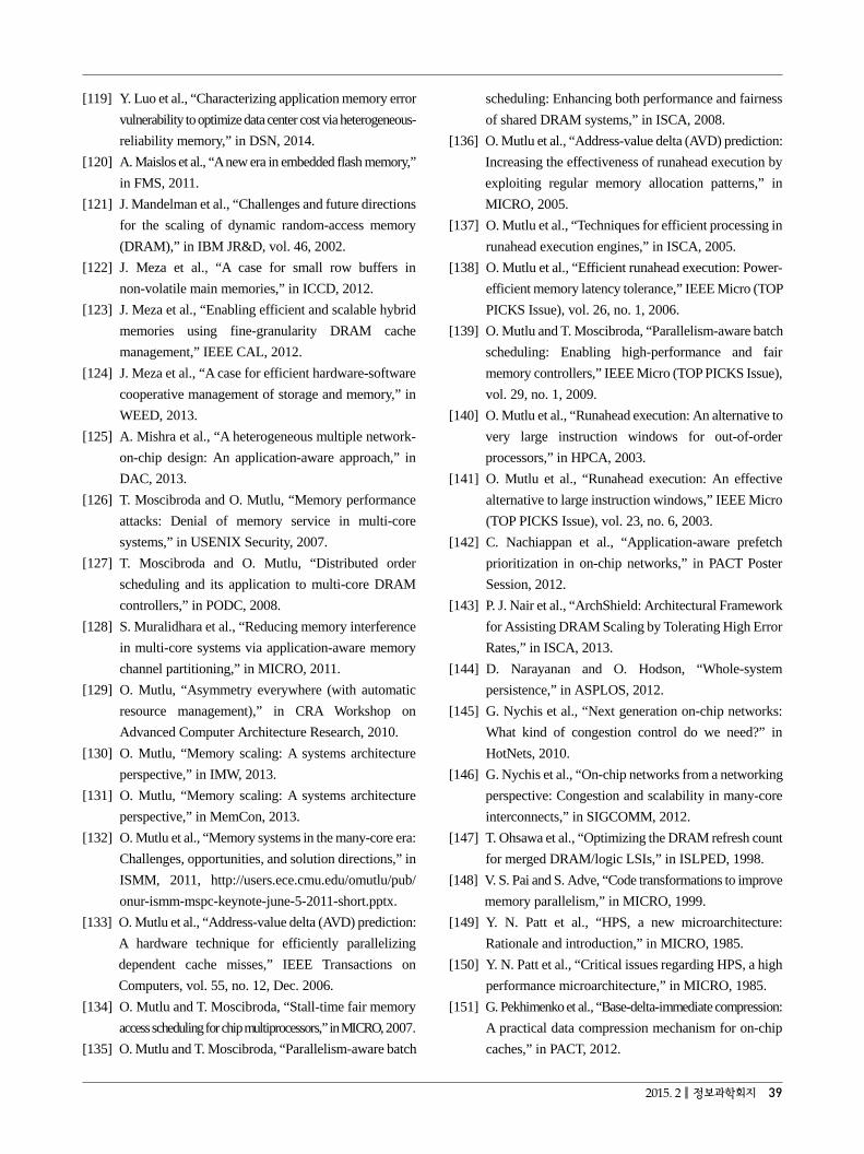
2015. 2 정보과학회지 39
[119] Y. Luo et al., “Characterizing application memory error vulnerability to optimize data center cost via heterogeneous- reliability memory,” in DSN, 2014.
[120] A. Maislos et al., “A new era in embedded flash memory,” in FMS, 2011.
[121] J. Mandelman et al., “Challenges and future directions for the scaling of dynamic random-access memory (DRAM),” in IBM JR&D, vol. 46, 2002.
[122] J. Meza et al., “A case for small row buffers in non-volatile main memories,” in ICCD, 2012.
[123] J. Meza et al., “Enabling efficient and scalable hybrid memories using fine-granularity DRAM cache management,” IEEE CAL, 2012.
[124] J. Meza et al., “A case for efficient hardware-software cooperative management of storage and memory,” in WEED, 2013.
[125] A. Mishra et al., “A heterogeneous multiple network- on-chip design: An application-aware approach,” in DAC, 2013.
[126] T. Moscibroda and O. Mutlu, “Memory performance attacks: Denial of memory service in multi-core systems,” in USENIX Security, 2007.
[127] T. Moscibroda and O. Mutlu, “Distributed order scheduling and its application to multi-core DRAM controllers,” in PODC, 2008.
[128] S. Muralidhara et al., “Reducing memory interference in multi-core systems via application-aware memory channel partitioning,” in MICRO, 2011.
[129] O. Mutlu, “Asymmetry everywhere (with automatic resource management),” in CRA Workshop on Advanced Computer Architecture Research, 2010.
[130] O. Mutlu, “Memory scaling: A systems architecture perspective,” in IMW, 2013.
[131] O. Mutlu, “Memory scaling: A systems architecture perspective,” in MemCon, 2013.
[132] O. Mutlu et al., “Memory systems in the many-core era: Challenges, opportunities, and solution directions,” in ISMM, 2011, http://users.ece.cmu.edu/omutlu/pub/ onur-ismm-mspc-keynote-june-5-2011-short.pptx.
[133] O. Mutlu et al., “Address-value delta (AVD) prediction: A hardware technique for efficiently parallelizing dependent cache misses,” IEEE Transactions on Computers, vol. 55, no. 12, Dec. 2006.
[134] O. Mutlu and T. Moscibroda, “Stall-time fair memory access scheduling for chip multiprocessors,” in MICRO, 2007.
[135] O. Mutlu and T. Moscibroda, “Parallelism-aware batch
scheduling: Enhancing both performance and fairness of shared DRAM systems,” in ISCA, 2008.
[136] O. Mutlu et al., “Address-value delta (AVD) prediction: Increasing the effectiveness of runahead execution by exploiting regular memory allocation patterns,” in MICRO, 2005.
[137] O. Mutlu et al., “Techniques for efficient processing in runahead execution engines,” in ISCA, 2005.
[138] O. Mutlu et al., “Efficient runahead execution: Power- efficient memory latency tolerance,” IEEE Micro (TOP PICKS Issue), vol. 26, no. 1, 2006.
[139] O. Mutlu and T. Moscibroda, “Parallelism-aware batch scheduling: Enabling high-performance and fair memory controllers,” IEEE Micro (TOP PICKS Issue), vol. 29, no. 1, 2009.
[140] O. Mutlu et al., “Runahead execution: An alternative to very large instruction windows for out-of-order processors,” in HPCA, 2003.
[141] O. Mutlu et al., “Runahead execution: An effective alternative to large instruction windows,” IEEE Micro (TOP PICKS Issue), vol. 23, no. 6, 2003.
[142] C. Nachiappan et al., “Application-aware prefetch prioritization in on-chip networks,” in PACT Poster Session, 2012.
[143] P. J. Nair et al., “ArchShield: Architectural Framework for Assisting DRAM Scaling by Tolerating High Error Rates,” in ISCA, 2013.
[144] D. Narayanan and O. Hodson, “Whole-system persistence,” in ASPLOS, 2012.
[145] G. Nychis et al., “Next generation on-chip networks: What kind of congestion control do we need?” in HotNets, 2010.
[146] G. Nychis et al., “On-chip networks from a networking perspective: Congestion and scalability in many-core interconnects,” in SIGCOMM, 2012.
[147] T. Ohsawa et al., “Optimizing the DRAM refresh count for merged DRAM/logic LSIs,” in ISLPED, 1998.
[148] V. S. Pai and S. Adve, “Code transformations to improve memory parallelism,” in MICRO, 1999.
[149] Y. N. Patt et al., “HPS, a new microarchitecture: Rationale and introduction,” in MICRO, 1985.
[150] Y. N. Patt et al., “Critical issues regarding HPS, a high performance microarchitecture,” in MICRO, 1985.
[151] G. Pekhimenko et al., “Base-delta-immediate compression: A practical data compression mechanism for on-chip caches,” in PACT, 2012.
40 특집원고Ⅰ The Main Memory System: Challenges and Opportunities
[152] G. Pekhimenko et al., “Linearly compressed pages: A main memory compression framework with low complexity and low latency.” in MICRO, 2013.
[153] G. Pekhimenko et al., “Exploiting compressed block size as an indicator of future reuse,” in HPCA, 2015.
[154] S. Phadke and S. Narayanasamy, “MLP aware heterogeneous memory system,” in DATE, 2011.
[155] M. K. Qureshi et al., “Line distillation: Increasing cache capacity by filtering unused words in cache lines,” in HPCA, 2007.
[156] M. K. Qureshi et al., “Enhancing lifetime and security of phase change memories via start-gap wear leveling.” in MICRO, 2009.
[157] M. K. Qureshi et al., “Scalable high performance main memory system using phase-change memory technology,” in ISCA, 2009.
[158] M. K. Qureshi et al., “A case for MLP-aware cache replacement,” in ISCA, 2006.
[159] M. K. Qureshi and Y. N. Patt, “Utility-based cache partitioning: A low-overhead, high-performance, runtime mechanism to partition shared caches,” in MICRO, 2006.
[160] L. E. Ramos et al., “Page placement in hybrid memory systems,” in ICS, 2011.
[161] S. Raoux et al., “Phase-change random access memory: A scalable technology,” IBM JR&D, vol. 52, Jul/Sep 2008.
[162] B. Schroder et al., “DRAM errors in the wild: A large-scale field study,” in SIGMETRICS, 2009.
[163] N. H. Seong et al., “Tri-level-cell phase change memory: Toward an efficient and reliable memory system,” in ISCA, 2013.
[164] V. Seshadri et al., “The evicted-address filter: A unified mechanism to address both cache pollution and thrashing,” in PACT, 2012.
[165] V. Seshadri et al., “RowClone: Fast and efficient In-DRAM copy and initialization of bulk data,” in MICRO, 2013.
[166] V. Seshadri et al., “The dirty-block index,” in ISCA, 2014.[167] V. Seshadri et al., “Mitigating prefetcher-caused pollution
using informed caching policies for prefetched blocks,” TACO, 2014.
[168] F. Soltis, “Inside the AS/400,” 29th Street Press, 1996.[169] N. H. Song et al., “Security refresh: prevent malicious
wear-out and increase durability for phase-change memory with dynamically randomized address mapping,” in ISCA, 2010.
[170] V. Sridharan and D. Liberty, “A study of DRAM failures
in the field,” in SC, 2012.[171] V. Sridharan et al., “Feng shui of supercomputer
memory: Positional effects in DRAM and SRAM faults,” in SC, 2013.
[172] S. Srinath et al., “Feedback directed prefetching: Improving the performance and bandwidth-efficiency of hardware prefetchers,” in HPCA, 2007.
[173] J. Stuecheli et al., “The virtual write queue: Coordinating DRAM and last-level cache policies,” in ISCA, 2010.
[174] L. Subramanian et al., “MISE: Providing performance predictability and improving fairness in shared main memory systems,” in HPCA, 2013.
[175] L. Subramanian et al., “The blacklisting memory scheduler: Achieving high performance and fairness at low cost,” in ICCD, 2014.
[176] M. A. Suleman et al., “Accelerating critical section execution with asymmetric multi-core architectures,” in ASPLOS, 2009.
[177] M. A. Suleman et al., “Data marshaling for multi-core architectures,” in ISCA, 2010.
[178] M. A. Suleman et al., “Data marshaling for multi-core systems,” IEEE Micro (TOP PICKS Issue), vol. 31, no. 1, 2011.
[179] M. A. Suleman et al., “Accelerating critical section execution with asymmetric multi-core architectures,” IEEE Micro (TOP PICKS Issue), vol. 30, no. 1, 2010.
[180] L. Tang et al., “The impact of memory subsystem resource sharing on datacenter applications,” in ISCA, 2011.
[181] J. Tendler et al., “POWER4 system microarchitecture,” IBM JRD, Oct. 2001.
[182] M. Thottethodi et al., “Exploiting global knowledge to achieve self-tuned congestion control for k-ary n-cube networks,” IEEE TPDS, vol. 15, no. 3, 2004.
[183] R. M. Tomasulo, “An efficient algorithm for exploiting multiple arithmetic units,” IBM JR&D, vol. 11, Jan. 1967.
[184] T. Treangen and S. Salzberg, “Repetitive DNA and next-generation sequencing: computational challenges and solutions,” in Nature Reviews Genetics, 2012.
[185] A. Udipi et al., “Rethinking DRAM design and organization for energy-constrained multi-cores,” in ISCA, 2010.
[186] A. Udipi et al., “Combining memory and a controller with photonics through 3D-stacking to enable scalable and energy-efficient systems,” in ISCA, 2011.
[187] V. Vasudevan et al., “Using vector interfaces to deliver millions of IOPS from a networked key-value storage
2015. 2 정보과학회지 41
server,” in SoCC, 2012.[188] R. K. Venkatesan et al., “Retention-aware placement in
DRAM (RAPID): Software methods for quasi-non- volatile DRAM,” in HPCA, 2006.
[189] H. Volos et al., “Mnemosyne: lightweight persistent memory,” in ASPLOS, 2011.
[190] X. Wang and J. Martinez, “XChange: Scalable dynamic multi-resource allocation in multicore architectures,” in HPCA, 2015.
[191] H.-S. P. Wong et al., “Phase change memory,” in Proceedings of the IEEE, 2010.
[192] H.-S. P. Wong et al., “Metal-oxide RRAM,” in Proceedings of the IEEE, 2012.
[193] M. Xie et al., “Improving system throughput and fairness simultaneously in shared memory CMP systems via dynamic bank partitioning,” in HPCA, 2014.
[194] Y. Xie and G. H. Loh, “PIPP: Promotion/insertion pseudo-partitioning of multi-core shared caches,” in ISCA, 2009.
[195] H. Xin et al., “Accelerating read mapping with FastHASH,” in BMC Genomics, 2013.
[196] J. Yang et al., “Frequent value compression in data caches,” in MICRO, 2000.
[197] D. Yoon et al., “Adaptive granularity memory systems: A tradeoff between storage efficiency and throughput,” in ISCA, 2011.
[198] D. Yoon et al., “The dynamic granularity memory system,” in ISCA, 2012.
[199] H. Yoon et al., “Row buffer locality aware caching policies for hybrid memories,” in ICCD, 2012.
[200] H. Yoon et al., “Data mapping and buffering in multi-level cell memory for higher performance and energy efficiency.” CMU SAFARI Tech. Report, 2013.
[201] H. Yoon et al., “Efficient data mapping and buffering techniques for multi-level cell phase-change memories,” TACO, 2014.
[202] J. Zhao et al., “FIRM: Fair and high-performance memory control for persistent memory systems,” in MICRO, 2014.
[203] H. Zhou and T. M. Conte, “Enhancing memory level parallelism via recovery-free value prediction,” in ICS, 2003.
[204] S. Zhuravlev et al., “Addressing shared resource contention in multicore processors via scheduling,” in ASPLOS, 2010.
Onur Mutlu2006 PhD, Computer Engineering, University of
Texas at Austin2002 MSE, Computer Engineering, University of
Texasat Austin2000 BSE, Computer Engineering, University of
Michigan, Ann Arbor2000 BS, Psychology, University of Michigan, Ann Arbor2013~Present Dr. William D. and Nancy W. Strecker Early Career
(Associate) Professor, ECED ept., Carnegie Mellon University2009~Present Courtesy Assistant/Associate Professor, CS Dept., Carnegie
Mellon University2009~2013 Assistant Professor, ECE Dept., Carnegie Mellon University2006~2009 Researcher, Microsoft Research2007~2009 Research Fellow, University of Texas at Austin2004~2005 Co-op Engineer, Advanced Micro Devices (during summers)2001~2003 Graduate Technical Intern, Intel Corporation (during summers)2012 Intel Early Career Faculty Honor Program Award2012 CMU College of Engineering George Tallman Ladd Research
Award2011 IEEE Computer Society TCCA Young Computer Architect Award
Justin Meza2010~Present PhD Candidate, Electrical and Computer
Engineering, Carnegie Mellon University2014 MS, Electrical and Computer Engineering,
Carnegie Mellon University2010 BS, Computer Science, University of California
at Los Angeles2013~2014 Intern Researcher, Facebook2014 Intern Researcher, Google2006~2012 Intern Researcher, Hewlett-Packard Labs2013 John and Claire Bertucci Graduate Fellowship, Carnegie Mellon
University
Lavanya Subramanian2009~Present PhD Candidate, Electrical and Computer
Engineering, Carnegie Mellon University2012~Present MS, Electrical and Computer Engineering,
Carnegie Mellon University2007~Present Bachelors, Electronics and Communication
Engineering, Madras Institute of Technology, India2007~2009 Design Engineer, SanDisk2013 John and Claire Bertucci Graduate Fellowship, Carnegie Mellon
University2011 Graduate Technical Intern, Intel Corporation2010 Intern, Microsoft Research


![The Main Memory System: Challenges and …users.ece.cmu.edu/~omutlu/pub/main-memory-system_kiise15.pdf[29, 97] or resistive RAM (RRAM) [192] appear more scalable, have latency and](https://static.fdocuments.net/doc/165x107/5ad375db7f8b9a92258e84c5/the-main-memory-system-challenges-and-usersececmueduomutlupubmain-memory-system.jpg)