The Inconvenient Truths of NAND Flash Memory · The Inconvenient Truths of NAND Flash Memory Jim...
32
Santa Clara, CA USA August 2007 1 The Inconvenient Truths of NAND Flash Memory Jim Cooke ([email protected]) Applications Engineering Director Micron Technology, Inc.
Transcript of The Inconvenient Truths of NAND Flash Memory · The Inconvenient Truths of NAND Flash Memory Jim...
Santa Clara, CA USAAugust 2007 1
The Inconvenient Truths of NAND Flash Memory
Jim Cooke ([email protected])
Applications Engineering DirectorMicron Technology, Inc.
Santa Clara, CA USAAugust 2007 2
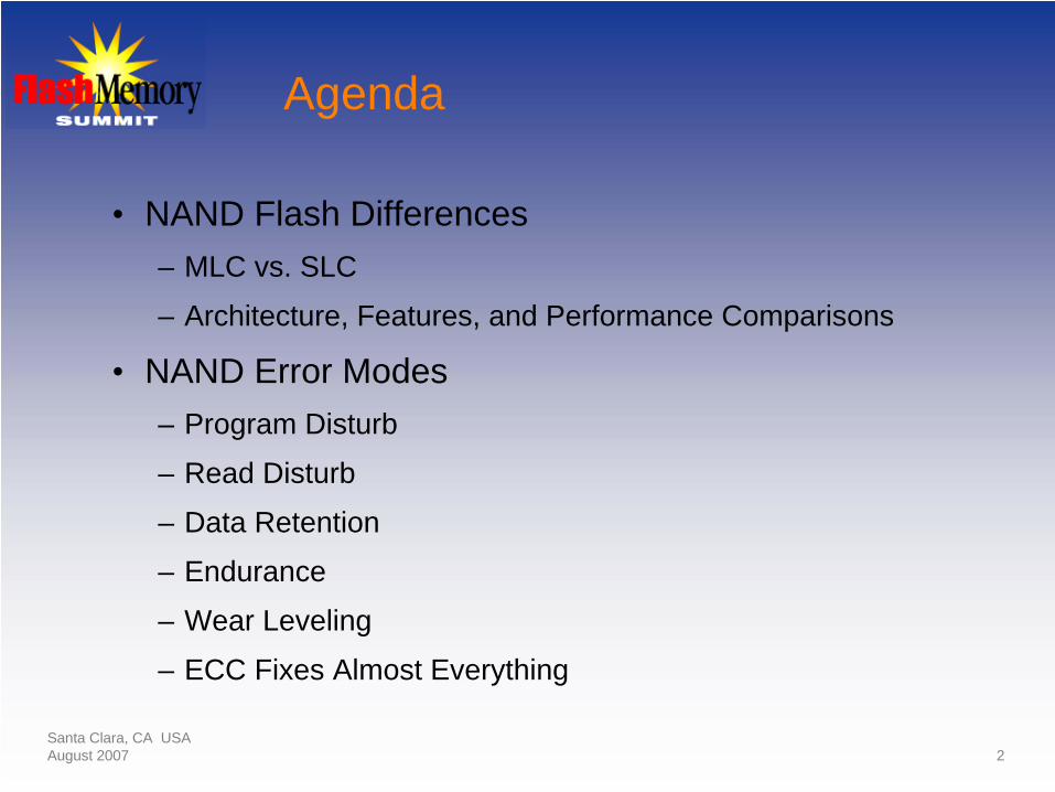
Agenda
• NAND Flash Differences – MLC vs. SLC
– Architecture, Features, and Performance Comparisons
• NAND Error Modes– Program Disturb
– Read Disturb
– Data Retention
– Endurance
– Wear Leveling
– ECC Fixes Almost Everything
Santa Clara, CA USAAugust 2007 3
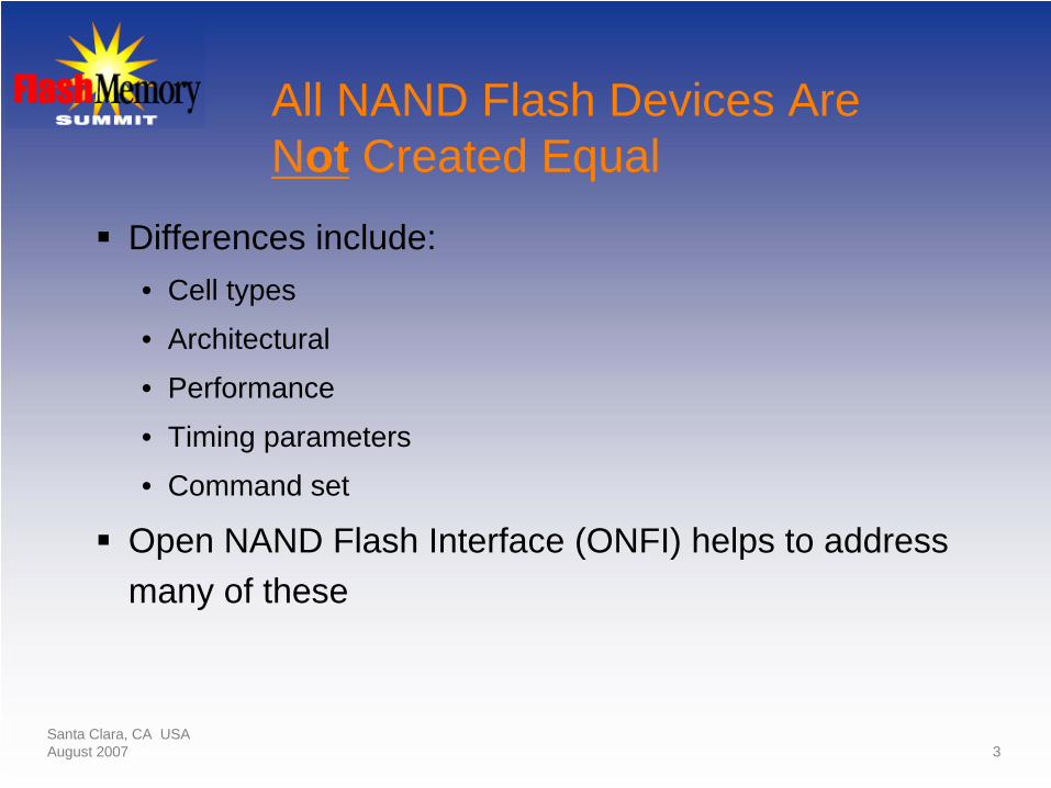
All NAND Flash Devices Are Not Created Equal
Differences include:• Cell types
• Architectural
• Performance
• Timing parameters
• Command set
Open NAND Flash Interface (ONFI) helps to address many of these
Santa Clara, CA USAAugust 2007 4
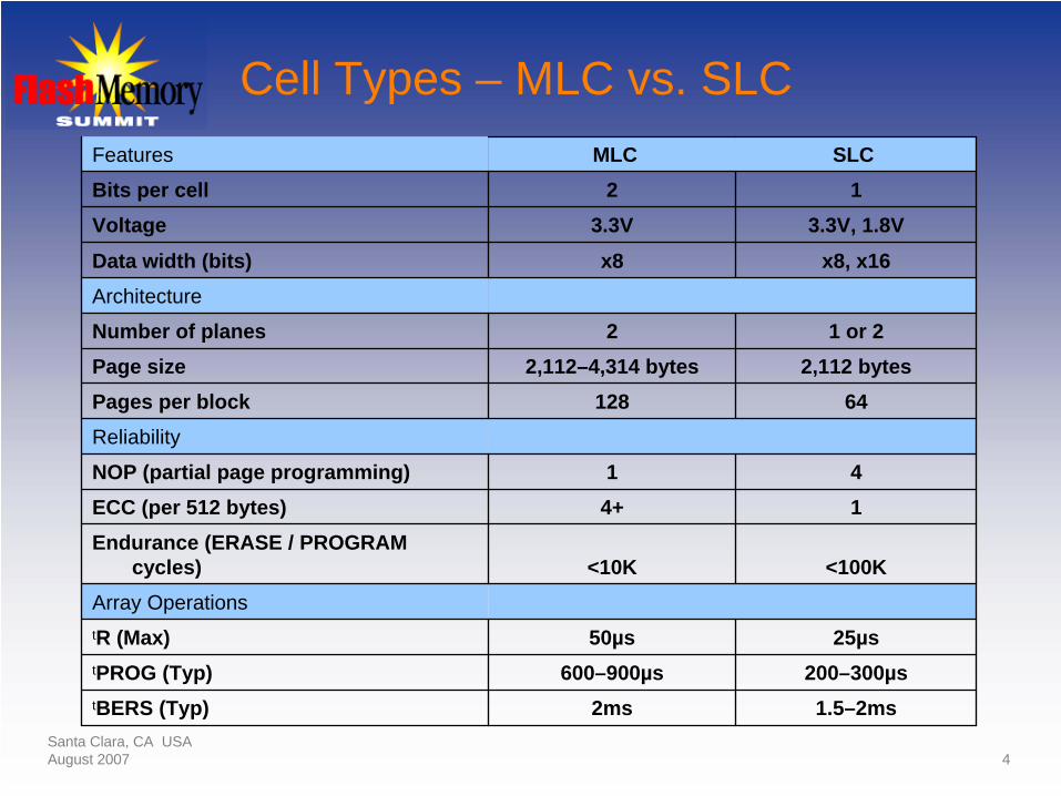
Cell Types – MLC vs. SLCFeatures MLC SLCBits per cell 2 1Voltage 3.3V 3.3V, 1.8V
Data width (bits) x8 x8, x16Architecture
Number of planes 2 1 or 2Page size 2,112–4,314 bytes 2,112 bytesPages per block 128 64Reliability
NOP (partial page programming) 1 4ECC (per 512 bytes) 4+ 1Endurance (ERASE / PROGRAM
cycles) <10K <100KArray OperationstR (Max) 50µs 25µstPROG (Typ) 600–900µs 200–300µstBERS (Typ) 2ms 1.5–2ms
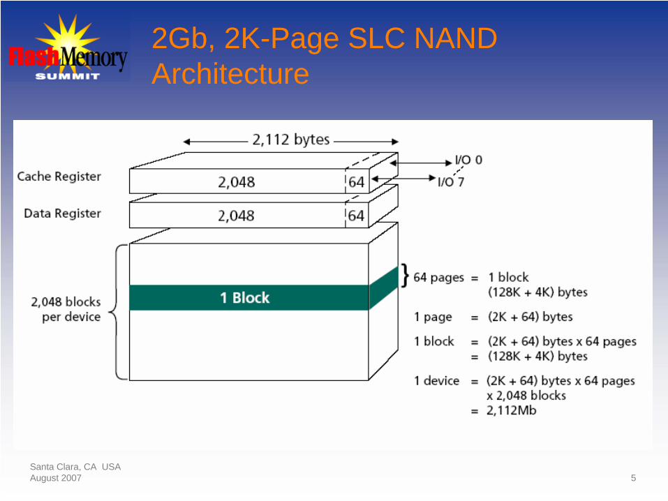
Santa Clara, CA USAAugust 2007 5
2Gb, 2K-Page SLC NAND Architecture
Santa Clara, CA USAAugust 2007 6
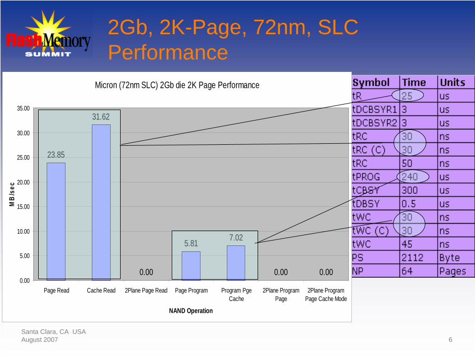
2Gb, 2K-Page, 72nm, SLC Performance
Micron (72nm SLC) 2Gb die 2K Page Performance
23.85
31.62
0.00
5.81 7.02
0.00 0.000.00
5.00
10.00
15.00
20.00
25.00
30.00
35.00
Page Read Cache Read 2Plane Page Read Page Program Program PgeCache
2Plane ProgramPage
2Plane ProgramPage Cache Mode
NAND Operation
MB
/sec
Santa Clara, CA USAAugust 2007 7
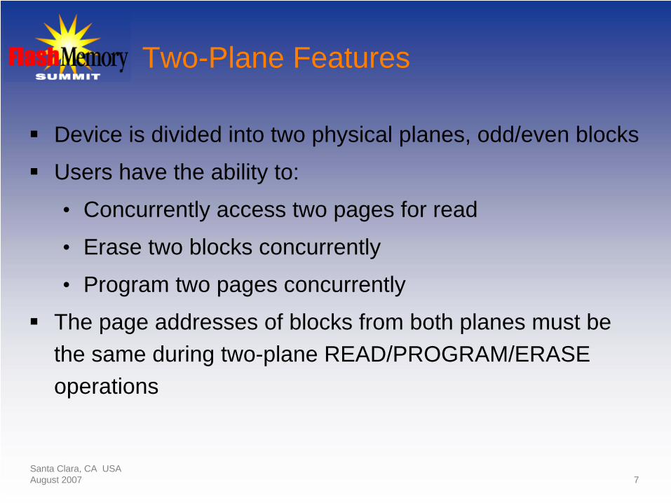
Two-Plane Features
Device is divided into two physical planes, odd/even blocks
Users have the ability to:
• Concurrently access two pages for read
• Erase two blocks concurrently
• Program two pages concurrently
The page addresses of blocks from both planes must be the same during two-plane READ/PROGRAM/ERASE operations
Santa Clara, CA USAAugust 2007 8
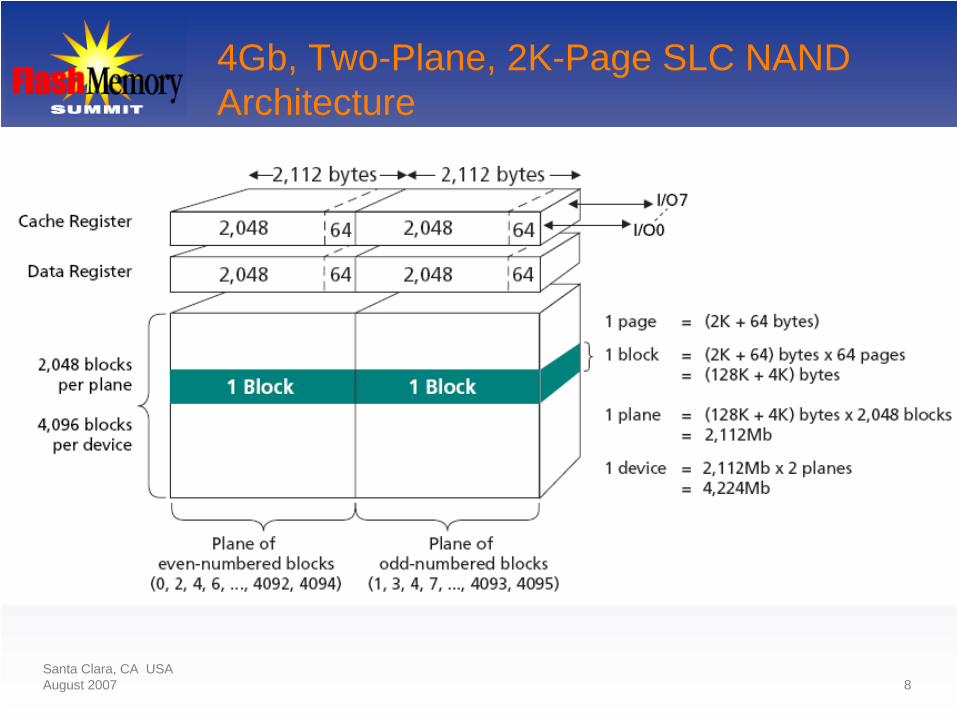
4Gb, Two-Plane, 2K-Page SLC NAND Architecture
Santa Clara, CA USAAugust 2007 9
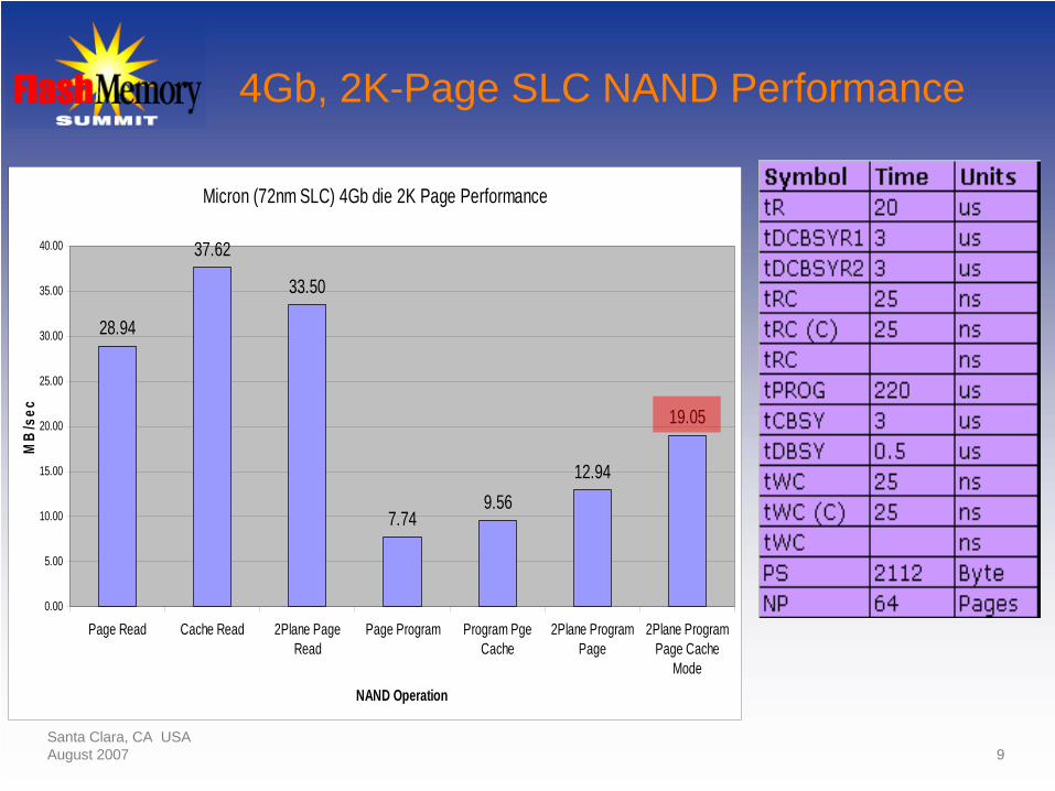
4Gb, 2K-Page SLC NAND Performance
Micron (72nm SLC) 4Gb die 2K Page Performance
28.94
37.62
33.50
7.749.56
12.94
19.05
0.00
5.00
10.00
15.00
20.00
25.00
30.00
35.00
40.00
Page Read Cache Read 2Plane PageRead
Page Program Program PgeCache
2Plane ProgramPage
2Plane ProgramPage Cache
Mode
NAND Operation
MB
/sec
Santa Clara, CA USAAugust 2007 10
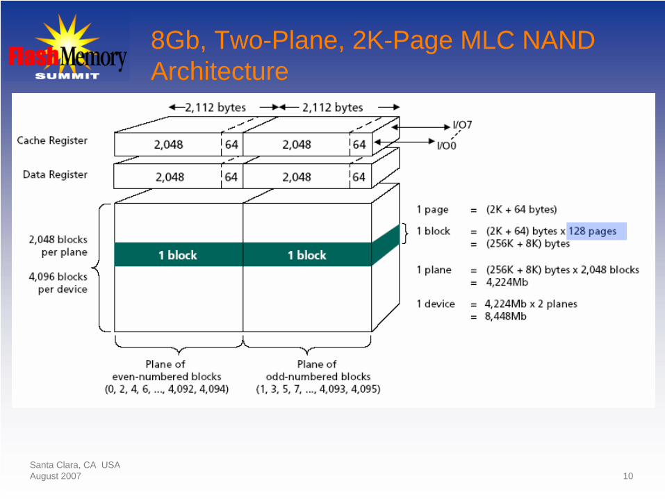
8Gb, Two-Plane, 2K-Page MLC NAND Architecture
Santa Clara, CA USAAugust 2007 11
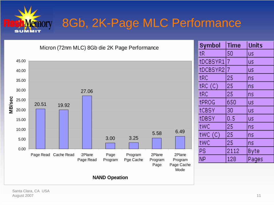
8Gb, 2K-Page MLC Performance
Micron (72nm MLC) 8Gb die 2K Page Performance
20.51 19.92
27.06
3.00 3.255.58 6.49
0.00
5.00
10.00
15.00
20.00
25.00
30.00
35.00
40.00
45.00
Page Read Cache Read 2PlanePage Read
PageProgram
ProgramPge Cache
2PlaneProgram
Page
2PlaneProgram
Page CacheMode
NAND Opeation
MB
/sec
Santa Clara, CA USAAugust 2007 12
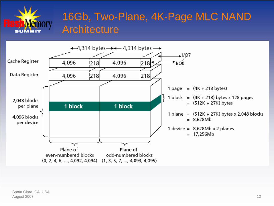
16Gb, Two-Plane, 4K-Page MLC NAND Architecture
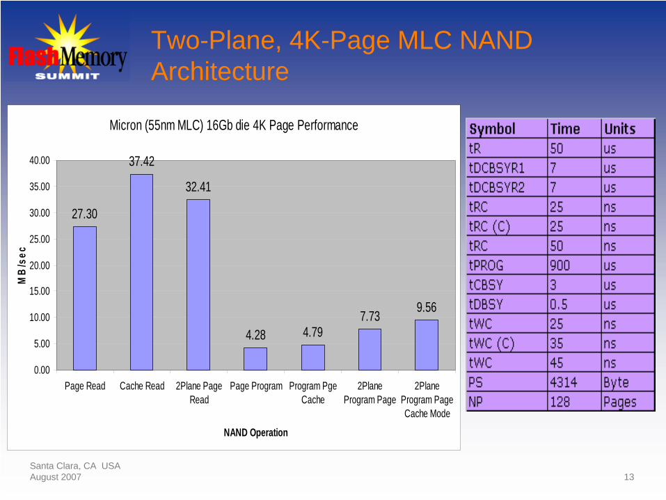
Santa Clara, CA USAAugust 2007 13
Two-Plane, 4K-Page MLC NAND Architecture
Micron (55nm MLC) 16Gb die 4K Page Performance
27.30
37.42
32.41
4.28 4.797.73 9.56
0.00
5.00
10.00
15.00
20.00
25.00
30.00
35.00
40.00
Page Read Cache Read 2Plane PageRead
Page Program Program PgeCache
2PlaneProgram Page
2PlaneProgram PageCache Mode
NAND Operation
MB
/sec

Santa Clara, CA USAAugust 2007 14
Open NAND Flash Interface
Future Micron NAND Flash devices support the ONFI specificationMicron is a founding member of ONFIThe ONFI 1.0 specification is available at http://www.onfi.org/ONFI founders:
Santa Clara, CA USAAugust 2007 15
NAND Error Modes
Program Disturb Read Disturb Data RetentionEndurance
Santa Clara, CA USAAugust 2007 16
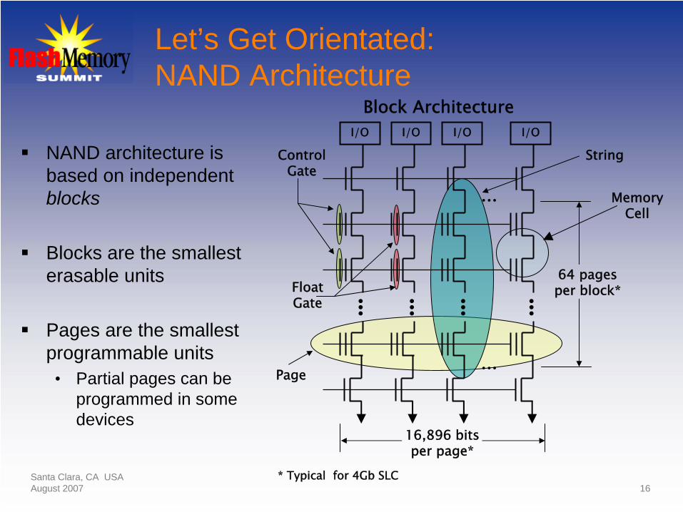
Let’s Get Orientated: NAND Architecture
NAND architecture is based on independent blocks
Blocks are the smallest erasable units
Pages are the smallest programmable units• Partial pages can be
programmed in some devices
16,896 bits per page*
64 pages per block*
Page
String
Float Gate
Memory Cell
Control Gate
I/OI/OI/OI/O
Block Architecture
* Typical for 4Gb SLC
Santa Clara, CA USAAugust 2007 17
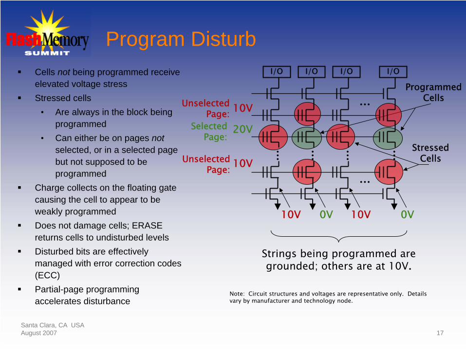
Program Disturb
10V
20V
10V
Selected Page:
Unselected Page:
UnselectedPage:
Strings being programmed are grounded; others are at 10V.
0V10V 10V 0V
Programmed Cells
Stressed Cells
Cells not being programmed receive elevated voltage stressStressed cells
• Are always in the block being programmed
• Can either be on pages not selected, or in a selected page but not supposed to be programmed
Charge collects on the floating gate causing the cell to appear to be weakly programmed Does not damage cells; ERASE returns cells to undisturbed levelsDisturbed bits are effectively managed with error correction codes (ECC)Partial-page programming accelerates disturbance
I/OI/OI/OI/O
Note: Circuit structures and voltages are representative only. Details vary by manufacturer and technology node.
Santa Clara, CA USAAugust 2007 18
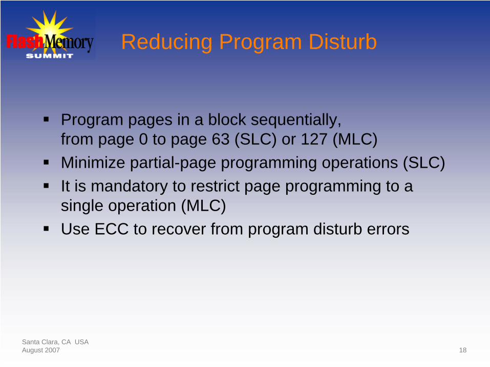
Reducing Program Disturb
Program pages in a block sequentially,from page 0 to page 63 (SLC) or 127 (MLC)Minimize partial-page programming operations (SLC)It is mandatory to restrict page programming to a single operation (MLC)Use ECC to recover from program disturb errors

Santa Clara, CA USAAugust 2007 19
Read Disturb
5V
0V
5V
Selected Page:
Unselected Page:
Unselected Page:
Stressed Cells
Cells not being read receive elevated voltage stressStressed cells are
• Always in the block being read
• Always on pages not being read
Charge collects on the floating gate causing the cell to appear to be weakly programmed Does not damage cells; ERASE returns cells to undisturbed levelsDisturbed bits are effectively managed with ECC
I/OI/OI/OI/O
Note: Circuit structures and voltages are representative only. Details vary by manufacturer and technology node.

Santa Clara, CA USAAugust 2007 20
Reducing Read Disturb
Rule of thumb for excessive reads per block between ERASE operations• SLC – 1,000,000 READ cycles
• MLC – 100,000 READ cycles
If possible, read equally from pages within the block
If exceeding the rule-of-thumb cycle count, then move the block to another location and erase the original block
Establish ECC threshold to move data
Erase resets the READ DISTURB cycle count
Use ECC to recover from read disturb errors
Santa Clara, CA USAAugust 2007 21
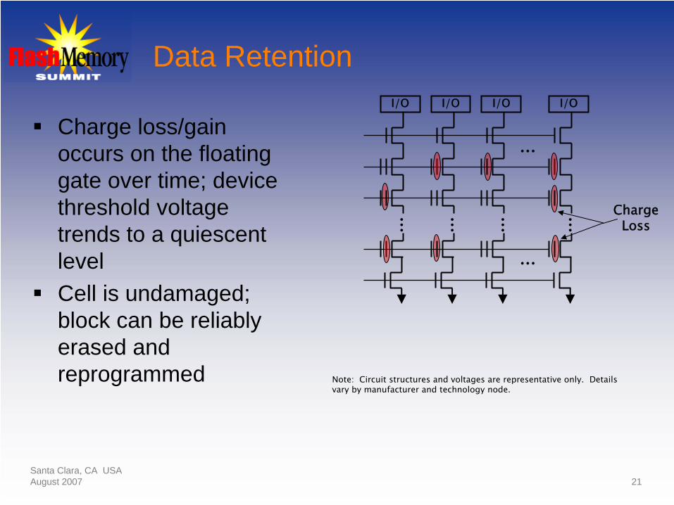
Data Retention
Charge loss/gain occurs on the floating gate over time; device threshold voltage trends to a quiescent levelCell is undamaged; block can be reliably erased and reprogrammed Note: Circuit structures and voltages are representative only. Details
vary by manufacturer and technology node.
Charge Loss
I/OI/OI/OI/O
Santa Clara, CA USAAugust 2007 22
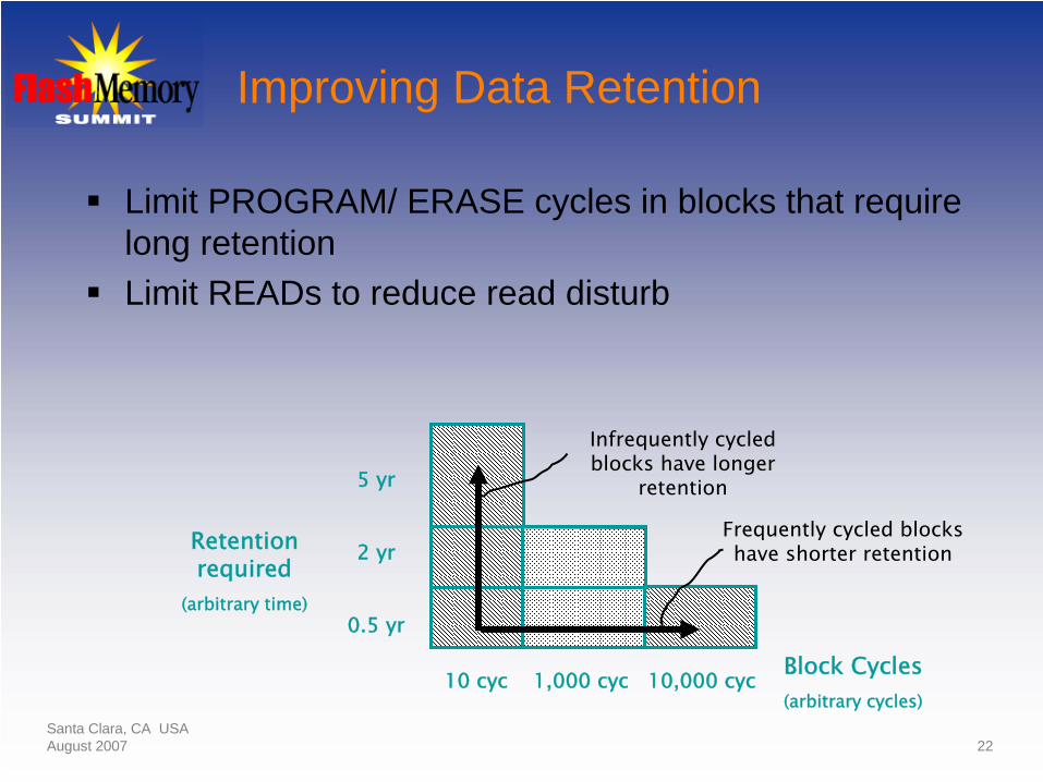
Improving Data Retention
Limit PROGRAM/ ERASE cycles in blocks that require long retentionLimit READs to reduce read disturb
10 cyc 1,000 cyc 10,000 cyc
5 yr
2 yr
0.5 yr
Retention required
(arbitrary time)
Block Cycles(arbitrary cycles)
Infrequently cycled blocks have longer
retention
Frequently cycled blocks have shorter retention
Santa Clara, CA USAAugust 2007 23
Endurance
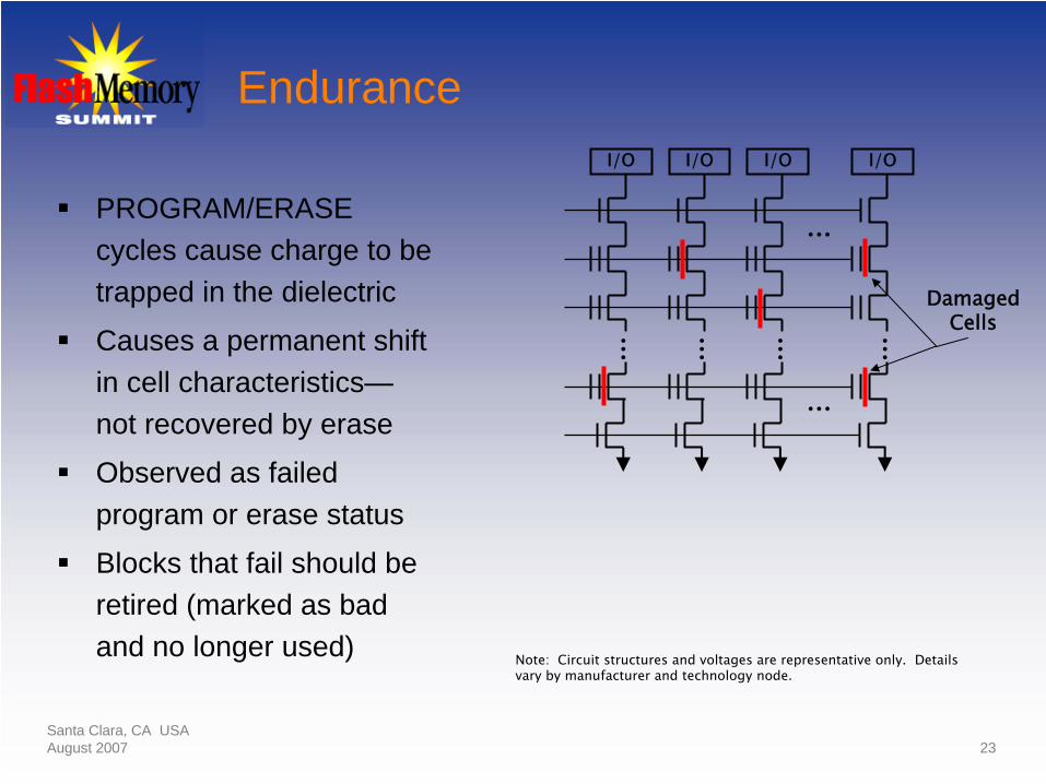
PROGRAM/ERASE cycles cause charge to be trapped in the dielectric
Causes a permanent shiftin cell characteristics—not recovered by erase
Observed as failed program or erase status
Blocks that fail should be retired (marked as bad and no longer used)
I/OI/OI/OI/O
Note: Circuit structures and voltages are representative only. Details vary by manufacturer and technology node.
Damaged Cells
Santa Clara, CA USAAugust 2007 24
Endurance Recommendations
Always check pass/fail status (SR0) for PROGRAM and ERASE operations• Note: READ operations do not set SR0 to fail
statusIf fail status after PROGRAM, move all block data to an available block and mark the failed block badUse ECC to recover from errorsWrite data equally to all good blocks (wear leveling)Protect block management/meta data in spare area with ECC
Santa Clara, CA USAAugust 2007 25
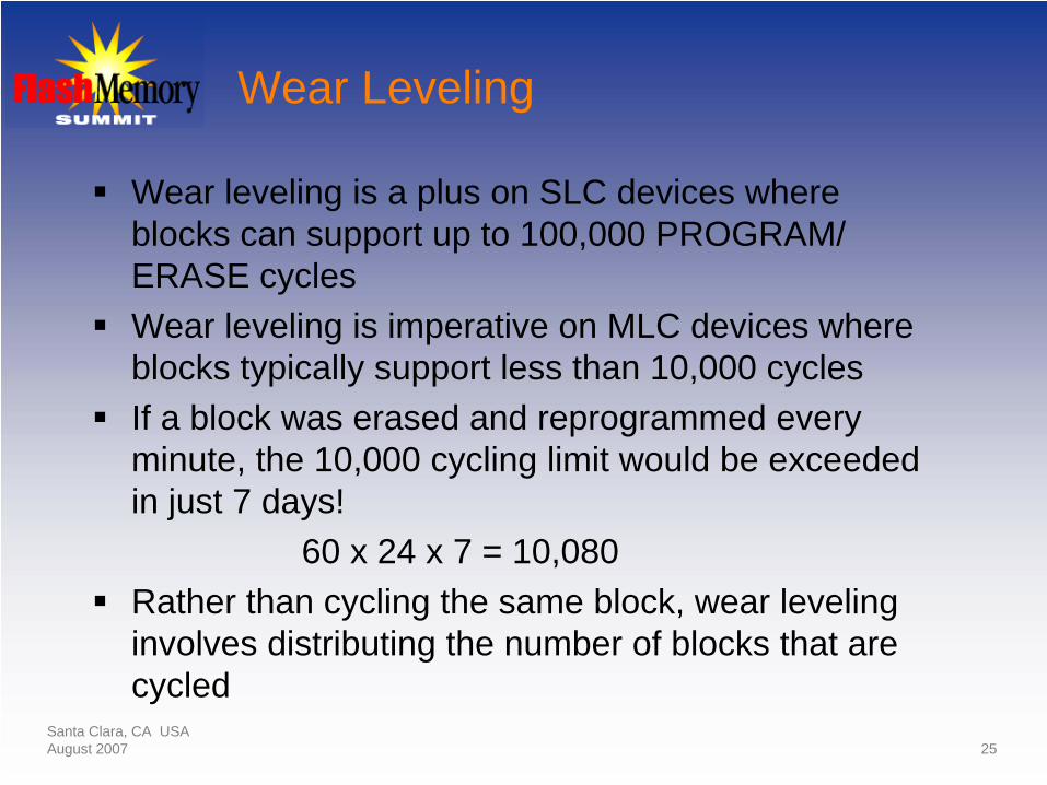
Wear Leveling
Wear leveling is a plus on SLC devices where blocks can support up to 100,000 PROGRAM/ ERASE cyclesWear leveling is imperative on MLC devices where blocks typically support less than 10,000 cyclesIf a block was erased and reprogrammed every minute, the 10,000 cycling limit would be exceeded in just 7 days!
60 x 24 x 7 = 10,080Rather than cycling the same block, wear leveling involves distributing the number of blocks that are cycled
Santa Clara, CA USAAugust 2007 26
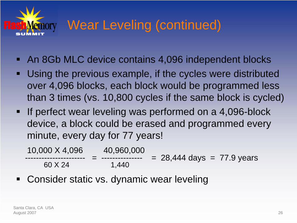
Wear Leveling (continued)
An 8Gb MLC device contains 4,096 independent blocksUsing the previous example, if the cycles were distributed over 4,096 blocks, each block would be programmed less than 3 times (vs. 10,800 cycles if the same block is cycled)If perfect wear leveling was performed on a 4,096-block device, a block could be erased and programmed every minute, every day for 77 years!10,000 X 4,096 40,960,000---------------------- = --------------- = 28,444 days = 77.9 years
60 X 24 1,440
Consider static vs. dynamic wear leveling
Santa Clara, CA USAAugust 2007 27
ECC Can Fix Everything (well, almost)
Understand the target data-error rate for your particular system
Understand the use model that you intend for your system
Design the ECC circuit to improve the raw-bit error rate (BER) of the NAND Flash, under your use conditions, to meet the system’s target BER
Santa Clara, CA USAAugust 2007 28
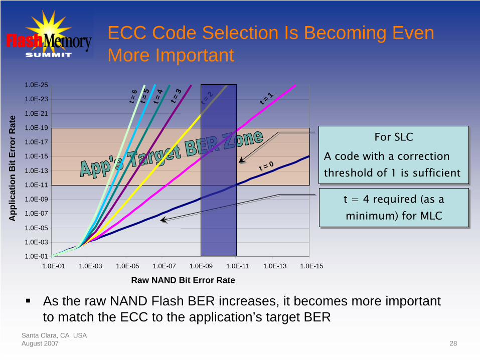
ECC Code Selection Is Becoming Even More Important
As the raw NAND Flash BER increases, it becomes more important to match the ECC to the application’s target BER
t = 0
t = 1
t = 2t = 3
t = 4
t = 5
t = 6
1.0E-25
1.0E-23
1.0E-21
1.0E-19
1.0E-17
1.0E-15
1.0E-13
1.0E-11
1.0E-09
1.0E-07
1.0E-05
1.0E-03
1.0E-011.0E-151.0E-131.0E-111.0E-091.0E-071.0E-051.0E-031.0E-01
Raw NAND Bit Error Rate
App
licat
ion
Bit
Erro
r Rat
e
For SLC
A code with a correction threshold of 1 is sufficient
For SLC
A code with a correction threshold of 1 is sufficient
t = 4 required (as a minimum) for MLC
t = 4 required (as a minimum) for MLC
Santa Clara, CA USAAugust 2007 29
Another Option: Embedded MMC (eMMC)
The complexities of future MLC require increased attention; the ECC algorithm, for example, is becoming more and more complex, moving from 4+ bits to 8+ bits in the futureA managed interface addresses the complexities of current and future NAND Flash devices; this means the host does not need to know the details of NAND Flash block sizes, page sizes, planes, new features, process generation, MLC vs. SLC, wear leveling, ECC requirements, etc. Embedded MMC (eMMC) is the next logical step in the NAND Flash evolution for embedded applications because it turns a program/ erase/read device with bad blocks and bad bits (NAND Flash) into a simple write/read memory
Santa Clara, CA USAAugust 2007 30
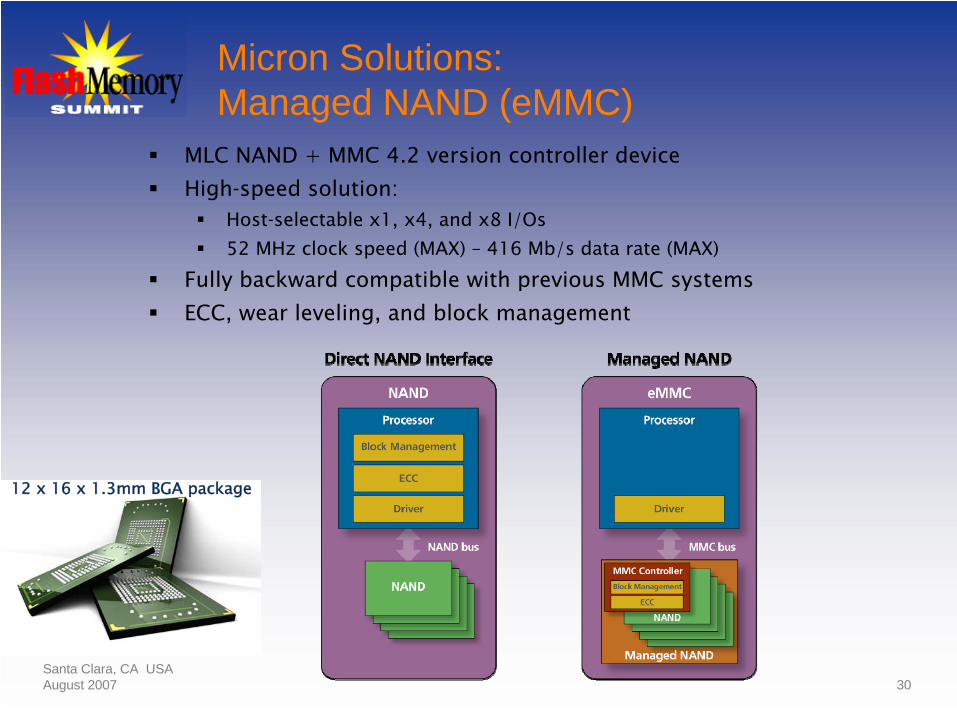
Micron Solutions: Managed NAND (eMMC)
MLC NAND + MMC 4.2 version controller deviceHighspeed solution:
Hostselectable x1, x4, and x8 I/Os52 MHz clock speed (MAX) – 416 Mb/s data rate (MAX)
Fully backward compatible with previous MMC systems ECC, wear leveling, and block management
12 x 16 x 1.3mm BGA package

Santa Clara, CA USAAugust 2007 31
Conclusions
NAND Flash is the lowest cost, nonvolatile memory available todayComplexities of MLC NAND require increased logic and software designAll of these complexities are addressed through the use of the controller included with eMMC
Santa Clara, CA USAAugust 2007 32
Thank You
©2007 Micron Technology, Inc. All rights reserved. Products are warranted only to meet Micron’s production data sheet specifications. Information, products and/or specifications are subject to change without notice. All information is provided on an “AS IS” basis without warranties of any kind. Dates are estimates only. Drawings not to scale. Micron and the Micron logo are trademarks of Micron Technology, Inc. All other trademarks are the property of their respective owners.