
The How, Why, When, and Where of Automated X-ray Test€¦ · Use of automated X-ray inspection ......
7
The Why, Where, What, How, and When of Automated X-ray Inspection By Glen Leinbach and Stig Oresjo Agilent Technologies Loveland, Colorado [email protected]; [email protected] ABSTRACT Use of automated X-ray inspection (AXI) for printed circuit board inspection is rapidly growing, especially on high-density, complex boards. X-ray images of solder joints can be analyzed automatically to detect structural defects, such as insufficient solder, voiding, shorts, opens, and other defects – that typically make up 80% to 90% of the total defects on an assembled circuit board. How do the different AXI technologies work? What are the appropriate uses of 2D versus 3D X-ray? Where in the manufacturing process should AXI be placed for maximum effect? And, not least, how can AXI be used to improve the manufacturing process? THE NEED FOR BETTER TEST For many years, the de facto test process for production of printed circuit board assemblies (PCBAs) included manual visual inspection (MVI) after soldering followed by an electrical test such as in-circuit test (ICT) at the end of the assembly process to isolate any defects that occurred during manufacturing. A final functional test was then run to verify that the product worked as required before it was integrated into the final product. This process was sufficient until the advent of surface mount technology (SMT). SMT allowed quantum advances in circuit density over through-hole technology (THT) due to much smaller packages with smaller leads. Once they were comfortable with single-sided SMT, designers began placing components on both sides of the PCBAs to obtain the most functionality in the smallest possible package. As this was happening, production rates increased for consumer products, such as cell phones, and the large complex boards used in servers, routers, and telecom equipment grew larger and more complex. Yields at functional test dropped, and large numbers of skilled technicians were needed for troubleshooting. It became clear that a new test method was needed to find manufacturing defects. Looking at a table of defects commonly found in on PCBAs during assembly, it is obvious that most are not electrical defects, but "structural" defects. Defect Type Approximate Occurrence Rate Defect Class Solder Related Open 25% Structural Yes Insufficient 18% Structural Yes Short 13% Structural Yes Missing Electrical Comp. 12% Structural No Misaligned 8% Structural Yes Defective Electrical Comp. 8% Electrical No Wrong Component 5% Electrical No Excess Solder 3% Structural Yes Missing Non-electrical Comp. 2% Structural Yes Wrong Orientation 2% Electrical No Defective Non-electrical Comp. 2% Structural No Extra 2% Electrical Yes Figure 1 1 Although electrical test is effective at finding many structural defects, such as shorts and missing components, a structural test would be a better fit to the types of defects occurring in manufacturing. WHY X-RAY INSPECTION? There are many forms of structural test and inspection in industrial use: X-ray, optical, ultrasonic, thermal imaging, etc. As seen in Table 1, many of the defects are related to the soldering process. X-ray has a unique advantage over other structural test technologies: Materials absorb X-rays proportional to their atomic weight. Materials made of heavier elements absorb more X-rays and are easily imaged, while materials made of lighter elements are more transparent to X-rays. Solders used in electronic assembly are made of heavy elements, such as tin, bismuth, silver, indium, and lead. Most other materials used in electronics are made of lighter elements, such as carbon, aluminum, oxygen, hydrogen, silicon, sodium, and copper.
Transcript of The How, Why, When, and Where of Automated X-ray Test€¦ · Use of automated X-ray inspection ......

The Why, Where, What, How, and When of Automated X-ray Inspection
By Glen Leinbach and Stig OresjoAgilent TechnologiesLoveland, [email protected]; [email protected]
ABSTRACTUse of automated X-ray inspection (AXI) forprinted circuit board inspection is rapidlygrowing, especially on high-density, complexboards. X-ray images of solder joints can beanalyzed automatically to detect structuraldefects, such as insufficient solder, voiding,shorts, opens, and other defects – that typicallymake up 80% to 90% of the total defects on anassembled circuit board. How do the differentAXI technologies work? What are theappropriate uses of 2D versus 3D X-ray? Wherein the manufacturing process should AXI beplaced for maximum effect? And, not least, howcan AXI be used to improve the manufacturingprocess?
THE NEED FOR BETTER TESTFor many years, the de facto test process forproduction of printed circuit board assemblies(PCBAs) included manual visual inspection(MVI) after soldering followed by an electricaltest such as in-circuit test (ICT) at the end of theassembly process to isolate any defects thatoccurred during manufacturing. A finalfunctional test was then run to verify that theproduct worked as required before it wasintegrated into the final product. This processwas sufficient until the advent of surface mounttechnology (SMT). SMT allowed quantumadvances in circuit density over through-holetechnology (THT) due to much smaller packageswith smaller leads. Once they were comfortablewith single-sided SMT, designers began placingcomponents on both sides of the PCBAs toobtain the most functionality in the smallestpossible package. As this was happening,production rates increased for consumerproducts, such as cell phones, and the largecomplex boards used in servers, routers, andtelecom equipment grew larger and morecomplex. Yields at functional test dropped, andlarge numbers of skilled technicians were neededfor troubleshooting. It became clear that a newtest method was needed to find manufacturingdefects.
Looking at a table of defects commonly found inon PCBAs during assembly, it is obvious thatmost are not electrical defects, but "structural"defects.
Defect Type ApproximateOccurrenceRate
Defect Class SolderRelated
Open 25% Structural YesInsufficient 18% Structural YesShort 13% Structural YesMissing Electrical Comp. 12% Structural NoMisaligned 8% Structural YesDefective ElectricalComp.
8% Electrical No
Wrong Component 5% Electrical NoExcess Solder 3% Structural YesMissing Non-electricalComp.
2% Structural Yes
Wrong Orientation 2% Electrical NoDefective Non-electricalComp.
2% Structural No
Extra 2% Electrical YesFigure 11
Although electrical test is effective at findingmany structural defects, such as shorts andmissing components, a structural test would be abetter fit to the types of defects occurring inmanufacturing.
WHY X-RAY INSPECTION?There are many forms of structural test andinspection in industrial use: X-ray, optical,ultrasonic, thermal imaging, etc. As seen inTable 1, many of the defects are related to thesoldering process. X-ray has a unique advantageover other structural test technologies: Materialsabsorb X-rays proportional to their atomicweight. Materials made of heavier elementsabsorb more X-rays and are easily imaged, whilematerials made of lighter elements are moretransparent to X-rays. Solders used in electronicassembly are made of heavy elements, such astin, bismuth, silver, indium, and lead. Mostother materials used in electronics are made oflighter elements, such as carbon, aluminum,oxygen, hydrogen, silicon, sodium, and copper.
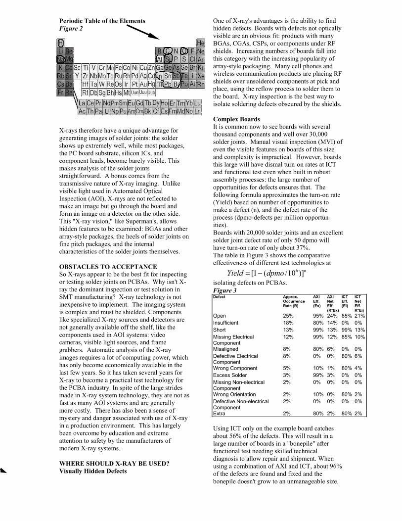
Periodic Table of the ElementsFigure 2
X-rays therefore have a unique advantage forgenerating images of solder joints: the soldershows up extremely well, while most packages,the PC board substrate, silicon ICs, andcomponent leads, become barely visible. Thismakes analysis of the solder jointsstraightforward. A bonus comes from thetransmissive nature of X-ray imaging. Unlikevisible light used in Automated OpticalInspection (AOI), X-rays are not reflected tomake an image but go through the board andform an image on a detector on the other side.This "X-ray vision," like Superman's, allowshidden features to be examined: BGAs and otherarray-style packages, the heels of solder joints onfine pitch packages, and the internalcharacteristics of the solder joints themselves.
OBSTACLES TO ACCEPTANCESo X-rays appear to be the best fit for inspectingor testing solder joints on PCBAs. Why isn't X-ray the dominant inspection or test solution inSMT manufacturing? X-ray technology is notinexpensive to implement. The imaging systemis complex and must be shielded. Componentslike specialized X-ray sources and detectors arenot generally available off the shelf, like thecomponents used in AOI systems: videocameras, visible light sources, and framegrabbers. Automatic analysis of the X-rayimages requires a lot of computing power, whichhas only become economically available in thelast few years. So it has taken several years forX-ray to become a practical test technology forthe PCBA industry. In spite of the large stridesmade in X-ray system technology, they are not asfast as many AOI systems and are generallymore costly. There has also been a sense ofmystery and danger associated with use of X-rayin a production environment. This has largelybeen overcome by education and extremeattention to safety by the manufacturers ofmodern X-ray systems.
WHERE SHOULD X-RAY BE USED?Visually Hidden Defects
One of X-ray's advantages is the ability to findhidden defects. Boards with defects not opticallyvisible are an obvious fit: products with manyBGAs, CGAs, CSPs, or components under RFshields. Increasing numbers of boards fall intothis category with the increasing popularity ofarray-style packaging. Many cell phones andwireless communication products are placing RFshields over unsoldered components at pick andplace, using the reflow process to solder them tothe board. X-ray inspection is the best way toisolate soldering defects obscured by the shields.
Complex BoardsIt is common now to see boards with severalthousand components and well over 30,000solder joints. Manual visual inspection (MVI) ofeven the visible features on boards of this sizeand complexity is impractical. However, boardsthis large will have dismal turn-on rates at ICTand functional test even when built in robustassembly processes: the large number ofopportunities for defects ensures that. Thefollowing formula approximates the turn-on rate(Yield) based on number of opportunities tomake a defect (n), and the defect rate of theprocess (dpmo-defects per million opportun-ities).Boards with 20,000 solder joints and an excellentsolder joint defect rate of only 50 dpmo willhave turn-on rate of only about 37%.The table in Figure 3 shows the comparativeeffectiveness of different test technologies at
isolating defects on PCBAs.Figure 3Defect Approx.
OccurrenceRate (R)
AXIEff.(Ex)
AXINetEff.(R*Ex)
ICTEff.(Ei)
ICTNetEff.R*Ei)
Open 25% 95% 24% 85% 21%Insufficient 18% 80% 14% 0% 0%Short 13% 99% 13% 99% 13%Missing ElectricalComponent
12% 99% 12% 85% 10%
Misaligned 8% 80% 6% 0% 0%Defective ElectricalComponent
8% 0% 0% 80% 6%
Wrong Component 5% 10% 1% 80% 4%Excess Solder 3% 99% 3% 0% 0%Missing Non-electricalComponent
2% 0% 0% 0% 0%
Wrong Orientation 2% 10% 0% 80% 2%Defective Non-electricalComponent
2% 0% 0% 0% 0%
Extra 2% 80% 2% 80% 2%
Using ICT only on the example board catchesabout 56% of the defects. This will result in alarge number of boards in a "bonepile" afterfunctional test needing skilled technicaldiagnosis to allow repair and shipment. Whenusing a combination of AXI and ICT, about 96%of the defects are found and fixed and the
ndpmoYield )]10/(1[ 6−=
bonepile doesn't grow to an unmanageable size.

High Reliability and Harsh EnvironmentsBoards used in aerospace or other high reliabilityapplications are a good fit for AXI since itevaluates the quality of the solder joints, not justtheir presence or absence. Similarly, productsused in harsh environments are well suited to X-ray inspection. Large thermal and mechanicalstresses on the board while in use cause marginaljoints to fail. An example is the under-hoodenvironment in automobiles. It is brutal, andfailure of an engine or braking control systemcan be catastrophic. Boards are not unusuallycomplex and are often single sided.
WHAT ARE THE VARIOUS X-RAYTECHNOLOGIES?X-ray is now accepted as one of the best methodsof isolating structural defects on PCBAs. Butwhat X-ray inspection and test technologies areavailable now and where do they give PCBAmanufacturers the most value?
Manual X-ray InspectionAlthough much more expensive thanconventional MVI, manual X-ray inspection issimilar: It uses the eyes and brain of the operatoras the image processor and decision-maker. LikeMVI, this is slow and boring in a productionenvironment resulting in inconsistent results andis better suited to a failure analysis environment.The operator doing failure analysis usually hasconsiderable expertise in X-ray image interpre-tation, and normally there is a limited number ofdefects to analyze. Most manual X-ray systemsare transmission systems.
2D or Transmission X-ray Inspection "2D" (two-dimensional) X-ray is another namefor conventional transmission X-ray technology.X-rays are generated at a fixed point source, passthrough the PCBA, and form an image on adetector. Most medical and dental X-rays aretransmission systems and use photographic filmas the detector. In manufacturing, an electronicdetector creates the image, converts it into adigital image and transfers it to a computerwhere analysis of the image takes place.As in a medical X-ray, everything between thesource and the detector is in focus. This workswell if you are looking at a broken bone or asingle sided PCBA that has only one layer ofsolder joints. On double-sided boards with ahigh density of solder joints on both sides of theboard, the image gets very confusing, as shownin Figure 4.Figure 4 2D Transmission Image
Solder joints from the top and bottom sides ofthe board overlap, shading each other andmaking analysis almost impossible. 2D X-raytest is best suited to single-sided boards and is
often used in automotive applications where highreliability is needed from single-sided boardsthat operate in a harsh environment. Many 2DX-ray inspection systems are in production useworldwide, usually on single-sided PCBAs.
The Need for 3D X-rayEngineers usually design double-sided boardsdue to performance or space requirements oftheir end products. These requirements oftenresult in poor electrical test access due to highdensity. This increased density and complexityare being seen in boards of ever increasing size;many as large as 18"x24". X-ray technology is adouble-edged sword: It allows imaging of hiddenfeatures, but also includes everything betweenthe X-ray source and detector in the image. It isclear that the solder joint information for eachside of a double-sided board must be separated tobe used effectively. For the purpose of thispaper, "3D" means that clear images of singlelayers (or slices) of the board are generated andused for test.
3D Digital TomosynthesisDigital tomosynthesis creates a pseudo-3Dimage by reconstructing multiple transmissionimages taken from different angles.
Figure 5 3D Tomosynthetic Image

The reconstruction of each slice is donecomputationally and requires a lot of computerpower. Integrating an infinite number of imageswould give the clearest, truest slice images.Unfortunately, the amount of computationincreases greatly as the number of images usedin the integration increases. Practicality limitsthe number of images used in eachreconstruction due to the throughput needs of aproduction system. The cost of reducing thenumber of images used results in the formationof phantom features or "artifacts" in the sliceimages that are a source of error in the analysisof the slice image. With today's throughputrequirements of PCBA production, digitaltomosynthesis is challenged to keep up.Implementation of digital tomosynthesis is stillvery limited in production environments butcontinues to be a promising technology ascomputers become faster and less costly.
Combining 2D and 3D TomosynthesisA novel approach is being offered that combinesthe speed of 2D transmission with the capabilityof 3D tomosynthesis. Many of the solder jointson double-sided boards are not shaded by jointson the other side of the board when viewed with2D transmission.In this combination technology, joints withoutshading are inspected with the faster 2D X-ray,and 3D digital tomosynthesis is used on thejoints that are shaded from the other side of theboard. This would seem to be a good approach,applying the strong points of each technology.Both the 2D and 3D imaging are done in onepass in the same system.
Fields of ViewDriven by the size and cost of X-ray detectors,limitations in system resolution, and the largequantity of data present in each image, all auto-mated X-ray systems divide the board under testinto smaller parts for imaging and analysis. Inmost systems, the size of these "fields of view"ranges from about 0.3-inch to 1.0-inch square.The theory behind the combination 2D/3D sys-tems is that a large percentage of solder joints arenot shaded and can therefore be inspected in 2Dmode. However, since the board must bedivided into views, the presence of any shadedjoints in a view requires that the entire view beinspected in 3D mode. This greatly increases thepercentage of the board that must be inspected inthe slower 3D tomosynthesis mode. The higherthe density of solder joints on the board, thehigher the likelihood that any view will require3D inspection due to shading.Figure 6 illustrates the percent of views that canbe inspected in 2D-transmission mode for sev-eral typical products. Results for two differentsized fields of view were calculated from realproduction board CAD data.
Figure 6
It is apparent that for high-density double-sidedboards there will not be much of a throughputadvantage in using 2D/3D combinational testingcompared to using 100% 3D tomosynthesis.
3D LaminographyIn 3D laminography, the X-ray source and thedetector move in a circular pattern, synchronizedbut 180 degrees out of phase. The X-ray imageis integrated around an entire revolution, digit-ized, and sent to the computer. In the image,only the features in one plane of the board are infocus.

Figure 7 3D Laminographic Image
Solder joints and anything else not in the planeof focus are sufficiently blurred out across theimage to allow independent analysis of the jointsin the plane of focus. By precisely moving theboard up and down (in the Z-axis), images ofjoints on each side of the board can be independ-ently generated for test. Since the image of eachside of the board is physically generated by theimaging system and not as a result of tomosyn-thetic computation, laminography is much fasterthan digital tomosynthesis. In a laminographicsystem, the ability to focus on a single slice ofthe board also requires the system to know wherethat desired slice is located in the Z-axis. Lami-nographic systems must measure the precise Z-axis position of the top and bottom of the board.Typically this is done on each board at thebeginning of the test cycle with a laser or opticalsystem that is an integral part of the system.Although this has a negative effect onthroughput, overall production rates oflaminographic systems are considerably fasterthan for existing 3D digital tomosynthesissystems. At present, there are several hundred3D X-ray laminography systems in use in PCBAmanufacturing worldwide.
WHEN SHOULD AXI BE USED?In the Assembly ProcessAutomated X-ray inspection can be useful atmany stages of the assembly process, but timeand resource constraints usually limit most
products to a single pass through X-ray. Itshould be implemented where it will have themaximum positive effect on the process. Sinceautomatic analysis of finished solder joints is itsstrength, most systems are placed after solderingprocesses, even though automated X-rayinspection is excellent for monitoring the solderpaste deposition process.Given a single X-ray inspection in the process,the best use is usually at the end of the finalsoldering process, be it either wave or reflow.All solder joints on the board are present and canbe covered in a single test. Also, by waitinguntil the completion of all assembly processes,any defects caused by the later processes (suchas damaged or missing components) will befound. The diagram in Figure 8 shows the flowfor a double-sided board with 2 reflow and aselective wave process.
Figure 8 Common Process Flow
Product LifecycleThe answer to another "when" question involvesthe life cycle of the product: Prototyping, earlyproduction, and volume production.PrototypingTo minimize the time to market for newproducts, the ability to turn-on and troubleshootprototype designs quickly is critical. This isparticularly difficult with large, complex boards:The designer is usually confronted with anunproven circuit design on an untested board thatprobably contains manufacturing defects.Finding and fixing the manufacturing defects cansave days or weeks in validating the design forproduction. Options in the prototyping phase aremanual visual inspection, electrical test with aflying prober, AOI, and AXI. ICT is not anormal option due to the lead-time for fixturingand programming. The flying prober has at leastthe same accessibility problems as ICT and onlyperforms shorts, opens, and analog in-circuitmeasurements. It is not very effective at findingmost solder defects, and work invested indeveloping a flying probe test can not beleveraged into production: A flying probercannot keep up with production volumes.Programs developed for AXI move with theproduct to production, so the investment inprototype test is not wasted.
Early ProductionThe value of AXI in volume production hasalready been discussed. Early low-volumeproduction can also have situations uniquelyanswered by AXI. Many manufacturers' normaltest methodology uses ICT as the predominantproduction test. Sometimes the ICT program orfixture is not ready when production begins.Due to its lack of fixturing and comparative easeof programming, an X-ray inspection can be

ready in a matter of hours or days and productioncan proceed without choking functional test withdifficult-to-isolate defects.
Volume ProductionWhen the ICT program and fixture becomeavailable and have been debugged, using bothICT and AXI as partners covers the largestdefect spectrum.
Defect Approx.OccuranceRate
AXIEff.
ICTEff.
AXI +ICTEFF.
Open 25% 95% 85% 99%Insufficient 18% 80% 0% 80%Short 13% 99% 99% 100%Missing ElectricalComponent
12% 99% 85% 100%
Misaligned 8% 80% 0% 80%Defective ElectricalComponent
8% 0% 80% 80%
Wrong Component 5% 10% 80% 82%Excess Solder 3% 99% 0% 99%Missing Non-electricalComponent
2% 0% 0% 0%
Wrong Orientation 2% 10% 80% 82%Defective Non-electricalComponent
2% 0% 0% 0%
Extra 2% 80% 80% 96%
Figures 9+10 Combined Effectiveness ofAXI+ICT
The key to this effectiveness is that eachtechnology complements the other. ICT candetect but not isolate shorts and cannot findintermittent open solder joints. AXI cannot findreversed ICs or wrong parts. Together theyassure that very few defects escape downstream.
PROCESS CONTROLUp to this point, the discussion has focused onautomated X-ray inspection being used forscreening defects on PCBAs. This has the mostimmediate and positive impact on the shipmentand quality performance of a manufacturer. Butwhile testing boards, automated X-ray inspectiongenerates information for two additionalopportunities to improve a shop's performance:attribute data (defects) and continuous(measurement) data about the solder joints.
Attribute DataBy recording defect data in a database andrunning periodic queries, a manufacturer canisolate and quantify manufacturing problems andtake corrective action. If problems are designrelated, hard data can often be used to convincedesigners to improve future designs.
Figure 11 Defects by Pin Number on U20
The example in Figure 11 shows how attributedata can be used for solving process problems.After the manufacturer sorted defects found byAXI by board type, defect type and componentreference designator. Defects on componentU20, a 0.5-mm pitch QFP64 package on the topof the board, were found to be much higher thanon any other part. Setting up another quickseries of Pareto charts indicated that the vastmajority of defects were solder bridges. The
AXI ICT

next Pareto showed that most were on pins 61and 62. (Figure 11.) The process engineer tookthis information to the solder paste-stencilingprocess, where a very small “dimple” was foundin the stencil between the apertures for pins 61and 62. This dimple allowed paste to besqueezed onto the board between the pins,causing a high occurrence of bridging. X-rayinspection generates detailed defect data that canlead to improved processes.Use of defect data, in conjunction with adatabase tool allowing the manufacturer to trackyields and isolate problems, can lead the way toimproving quality and assembly yields.
Measurement DataMeasurement data from x-ray inspection ofsolder joints gives the manufacturer informationneeded to implement real-time process control.At present, real-time process control is notcommonly used in PBCA manufacturing. It is adifficult environment for real-time processcontrol due to a large number of factors:• There are many possible causes for most
process variations.• The correlation between specific measure-
ment variations and their causes has notbeen well characterized by the industry. Alarge amount of work is needed to developthis characterization.
• In high mix shops, there are thousands ofuncontrolled variables, such as leadmaterial, finish, and size, the thermalcharacteristics of each product, and vendor-to-vendor component variations.
• The short life cycle of most products (oftensix months or less) and influx of newproducts makes characterization difficult.
• Product requirements often dictate that theboard's design is not an optimum fit with thePCBA assembly processes.
• The frequent transfer of products from line-to-line and facility-to-facility.
Today, the best fit for implementation of real-time SPC in PCBA manufacturing is in high-volume production facilities, building singleproducts over an extended period.Unique among test technologies, AXI collectsdetailed solder measurement data that only nowcan give the industry the information it needs forsuccessful SPC efforts. It promises to open newopportunities for major improvements in PCBAmanufacturing.
SUMMARYAutomated X-ray inspection is the most effectivetechnology for finding manufacturing defects inPCBA assembly operations. Its acceptance isincreasing and it is being successfully used inproduction and in prototype operations on manykinds of assemblies.
2D transmission is an excellent fit for single-sided PCBAs, and 3D AXI is the best fit forhigh-density double-sided boards.3D digital tomosynthesis is a very attractivetechnology for testing high-density double-sidedboards, but still lacks the throughput required formany applications. With improved throughputits use can become widely accepted. 3D laminography is a good fit for testing high-density double-sided boards. Its higherthroughput has resulted in successful productionimplementation at many facilities throughout theworld.Defect data is being used today to isolate andsolve many problems in production, and the datagenerated by AXI has the potential for use inprocess control as SMT manufacturing processesbecome characterized.When used in prototyping, all AXI technologiescontribute to minimizing the time to market fornew products. In production, AXI is the mosteffective method of finding manufacturingdefects. When coupled with electrical test in aproduction environment, manufacturers obtainthe broadest possible coverage of the PCBAdefect spectrum.
BIBLIOGRAPHY[1] Leinbach, Glen, "Using Production Defect
Data to Improve an SMT Assembly Process,"Proceedings of SMTA International 2000, pp.507-512
[2] Lecklider, Tom, "Faults Can't Hide From X-Ray Inspection," Evaluation Engineering,November 2000
[3] McClure, Doug, "X-rays spot circuit boardflaws," Machine Design, December 7, 2000


![Continuous Inspection - codemanshipcodemanship.co.uk/files/ContinuousInspection.pdf · Example Automated Continuous Inspection Process Change Code [before check-in] Run automated](https://static.fdocuments.net/doc/165x107/5f93d295a1c10d3ed34c6b1c/continuous-inspection-co-example-automated-continuous-inspection-process-change.jpg)


