The G-QRP Club Founded in 1974, the G-QRP Club is the largest QRP Club in the world. The club exists...
20
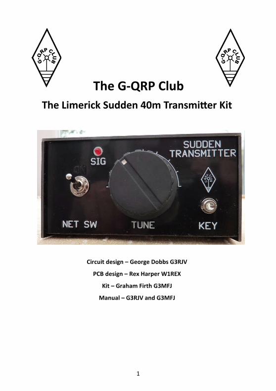
1 The G-QRP Club The Limerick Sudden 40m Transmier Kit Circuit design – George Dobbs G3RJV PCB design – Rex Harper W1REX Kit – Graham Firth G3MFJ Manual – G3RJV and G3MFJ
-
Upload
trinhthuan -
Category
Documents
-
view
224 -
download
3
Transcript of The G-QRP Club Founded in 1974, the G-QRP Club is the largest QRP Club in the world. The club exists...
1
The G-QRP Club
The Limerick Sudden 40m Transmi�er Kit
Circuit design – George Dobbs G3RJV
PCB design – Rex Harper W1REX
Kit – Graham Firth G3MFJ
Manual – G3RJV and G3MFJ

2
Founded in 1974, the G-QRP Club is the largest QRP Club in the world. The club exists to promote interest and growth in low power amateur radio communication (5 watts or less). Member-ship is open to any licensed radio amateur or short wave listener anywhere in the world.
The club publishes a quarterly journal called SPRAT, which is sent free to members. SPRAT contains many circuits, technical hints and ideas for QRP construction projects, together with club news, contest and award information and other items of interest to QRP operators. SPRAT is an exclusive QRP journal and con-tains much practical information in each issue. The club operates a club sales department where components are available at spe-cial prices to club members. We also publish QRP books which are available to members.
If you are not a member, and would like to find out more, please look at www.gqrp.com. For a sample SPRAT and a membership form, please send your name and address to our membership secretary:
Tony Fishpool, PO Box 298, Dartford, Kent. DA1 9DQ.
Please mention where you saw this information

3
Transmi�er Overview
The Limerick Sudden Transmi�er is a simple circuit for a reliable QRP transmi�er. Alt-
hough crystal controlled, the oscillator stage (T1) is a Variable Crystal Oscillator (VXO).
The crystal supplied is a fundamental frequency crystal on 7.030MHz, the QRP calling
frequency on the 40 metre band, although other frequencies are available for the CW
end of this band. No4ce that an inductor (L1) and a variable capacitor (VC1) have been
added in series with the crystal and ground. These induc4ve and capaci4ve elements
allow some shi6ing of the frequency.
The oscillator output is coupled via C4 to a 2N3904 Driver stage (T2). TR1 forms the RF
(radio frequency) load for the stage. It is also a coupling transformer to drive the power
amplifier. The transformer is wound on an FT37-43 core; a ferrite core for broadband
coupling. The primary winding is 25 turns of 30 s.w.g. enameled wire. (Gold) The sec-
ondary winding is 5 turns of the red wire wound over the centre of the primary winding.
The value of the resistance in the emi�er of T2 determines the amount of drive available
to T3 and hence the output power of the transmi�er. A preset poten4ometer (VR1) is
placed in series with R6 and acts as a DRIVE control.
The NPN 2N3906 transistor (T4) is used as a Key Switch to key the transmi�er. This keys
both the oscillator and the buffer/driver (T1 and T2). In many QRP transmi�er designs it
is common to leave the oscillator free running and to key later stages. This is because
keying an RF oscillator can result in a “chirpy” CW note. However, T1 is a crystal con-
trolled oscillator and no such chirp occurs. Keying both stages overcomes the problem
of oscillator break-through when the oscillator is s4ll running in the receive mode.
SW1 is a NET switch that enables the oscillator to run without keying the transmi�er. It
provides 12 volts for the oscillator and D1 prevents this voltage reaching T2. This facility
allows the oscillator to be heard in the receiver so that the VXO signal can be adjusted to
a desired frequency or aligned with a desired sta4on signal. “NeGng” is standard prac-
4ce when a separate transmi�er and receiver are being used; it is also called “spoGng”
in North America.
T3 is the transmi�er power amplifier (the Final). This is a simple Class C amplifier biased
by the drive voltage from TR1. The output load is provided by L2, an RF choke. A zener
diode (ZD1) offers protec4on for the output transistor should the transmi�er be inad-
vertently operated without an antenna or into a short circuit. A clip-on heat sink keeps
the transistor cool. C6 couples the RF output to a seven element Low-Pass Filter based
on the W3NQN filter data, with enhanced 2nd
harmonic filtering.
The capacitor C7 leads to the transmi�er-receiver break-in circuit popularized by W7EL
in his “Op4mised Transceiver” design. It is a simple method of sharing the same anten-
na by a transmi�er and receiver without damage to the receiver during transmission or
significant loss of signal from the transmi�er. Some mu4ng of the signal fed to the re-
ceiver is achieved by the circuit T5, T6 and T7. The mu4ng circuit is such that when a
receiver is connected to the transmi�er, 12 volts must be connected to the transmi�er
to hear signals. The mu4ng is most effec4ve when the covers are on the transmi�er and
receiver.

4
Building the Transmi�er
You will have no4ced that this is a rather unusual kit. It has a printed circuit board
without any holes. We call it “Limerick Construc4on” because it was designed by Rex
Harper, W1REX, of Limerick, Maine. It is a surface mounted board in that the compo-
nents are mounted on the surface of the board, although the components used are
“through-hole” parts. This allows for ease of construc4on and easy correc4on of any
errors. The main board also has the front and back panels for the transmi�er. They are
scored and can be snapped off the main board. We suggest you smooth the snapped
off edges with emery paper or an emery board. The component parts are soldered to
the top surface of the board using the leads that would go through the board on a
conven4onal printed circuit board. The interconnec4ons between the moun4ng pads
are ready made but hidden by the black screen printed overlay. The designa4on of all
the parts is printed next to the appropriate pads. Each sec4on of the transmi�er
(OSCILLATOR, DRIVER, FINAL, LOW-PASS FILTER and KEY SWITCH) is also marked on
the board. The MUTE circuit components are mounted on the back panel. Any refer-
ences to top, bo�om, le4 and right assume that the board is held with the printed text
the correct way, with the G-QRP Club logo in the centre right. Top is actually the Rear
of the finished board, and bo�om is, of course, the Front.
It does help to set out all the components in the order
of designa4on. i.e. C1, C2 etc. The best way is to use a
small piece of polystyrene to hold the individual parts.
If you are going to use this idea for semiconductors, a
piece of aluminium foil wrapped round the polystyrene
will prevent any sta4c damage. Double check the ca-
pacitor values—there is a lot of difference between a
101 and a 104 capacitor!
The building of the transmi�er does entail winding four
coils on toroid cores (TR1, and L4, L5 and L6), and an RF
choke for the PA wired on a pig-nosed binocular core
(L2). The cores are the small rings that look like miniature “Polo Mints”. L1 and L3 are
pre-wound chokes (coils) that look like fat resistors. Winding the coils is not difficult; it
just requires a li�le care and the accurate coun4ng of the number of turns. There is
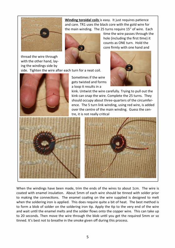
ample guidance in the pages of this manual. It is a good idea to wind TR1 before begin-
ning to add any other components to the board. It is the most difficult of the hand-
wound coils as it has two windings, a tuned winding and a smaller link winding.
TR1 is wound on the FT37-43 core. This is the black core - the one without the yellow
coa4ng. The primary winding has 25 turns of the gold wire. There is guide as to how
to wind these on the next page. Each 4me the wire passes through the hole of the core
counts as one turn. The turns should be laid side by side and occupy about three-
quarters of the circumference of the core. The link winding is 5 turns of the red wire
wound over the centre of the main winding. Placement of the link winding is not too
cri4cal – just guess the centre posi4on.
5
When the windings have been made, trim the ends of the wires to about 1cm. The wire is
coated with enamel insula4on. About 5mm of each wire should be 4nned with solder prior
to making the connec4ons. The enamel coa4ng on the wire supplied is designed to melt
when the soldering iron is applied. This does require quite a bit of heat. The best method is
to form a blob of solder on the soldering iron 4p. Apply the 4p to the very end of the wire
and wait un4l the enamel melts and the solder flows onto the copper wire. This can take up
to 20 seconds. Then move the wire through the blob un4l you get the required 5mm or so
4nned. It’s best not to breathe in the smoke given off during this process.
Winding toroidal coils is easy. It just requires pa4ence
and care. TR1 uses the black core with the gold wire for
the main winding. The 25 turns require 15” of wire. Each
4me the wire passes through the
hole (including the first 4me) it
counts as ONE turn. Hold the
core firmly with one hand and
thread the wire through
with the other hand, lay-
ing the windings side by
side. Tighten the wire a6er each turn for a neat coil.
Some4mes if the wire
gets twisted and forms
a loop it results in a
kink. Untwist the wire carefully. Trying to pull out the
kink can snap the wire. Complete the 25 turns. They
should occupy about three-quarters of the circumfer-
ence. The 5 turn link winding, using red wire, is added
over the centre of the main winding. Guess the cen-
tre, it is not really cri4cal
6
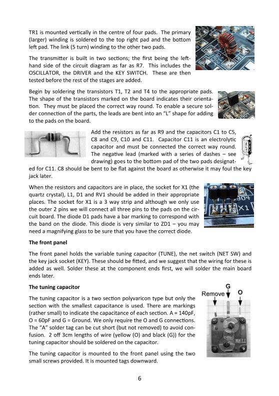
TR1 is mounted ver4cally in the centre of four pads. The primary
(larger) winding is soldered to the top right pad and the bo�om
le6 pad. The link (5 turn) winding to the other two pads.
The transmi�er is built in two sec4ons; the first being the le6-
hand side of the circuit diagram as far as R7. This includes the
OSCILLATOR, the DRIVER and the KEY SWITCH. These are then
tested before the rest of the stages are added.
Begin by soldering the transistors T1, T2 and T4 to the appropriate pads.
The shape of the transistors marked on the board indicates their orienta-
4on. They must be placed the correct way round. To enable a secure sol-
der connec4on of the parts, the leads are bent into an “L” shape for adding
to the pads on the board.
Add the resistors as far as R9 and the capacitors C1 to C5,
C8 and C9, C10 and C11. Capacitor C11 is an electroly4c
capacitor and must be connected the correct way round.
The nega4ve lead (marked with a series of dashes – see
drawing) goes to the bo�om pad of the two pads designat-
ed for C11. C8 should be bent to be flat against the board as otherwise it may foul the key
jack later.
When the resistors and capacitors are in place, the socket for X1 (the
quartz crystal), L1, D1 and RV1 should be added in their appropriate
places. The socket for X1 is a 3 way strip and although we only use
the outer 2 pins we will connect all three pins to the pads on the cir-
cuit board. The diode D1 pads have a bar marking to correspond with
the band on the diode. This diode is very similar to ZD1 – you may
need a magnifying glass to be sure that you have the correct diode.
The front panel
The front panel holds the variable tuning capacitor (TUNE), the net switch (NET SW) and
the key jack socket (KEY). These should be fi�ed, and we suggest that the wiring for these is
added as well. Solder these at the component ends first, we will solder the main board
ends later.
The tuning capacitor
The tuning capacitor is a two sec4on polyvaricon type but only the
sec4on with the smallest capacitance is used. There are markings
(rather small) to indicate the capacitance of each sec4on. A = 140pF,
O = 60pF and G = Ground. We only require the O and G connec4ons.
The “A” solder tag can be cut short (but not removed) to avoid con-
fusion. 2 off 3cm lengths of wire (yellow (O) and black (G)) for the
tuning capacitor should be soldered on the capacitor.
The tuning capacitor is mounted to the front panel using the two
small screws provided. It is mounted tags downward.

7
The key jack socket
The socket is a 3.5mm socket to be used with a 3.5mm mono jack plug
so one of the connec4ons, (which is a switch contact), is unused. It is a
good idea to cut off the unwanted solder tag to avoid confusion. The
ground tag should be to the outer edge. The wires for this will be sol-
dered to the main board first, and connected to the jack a6er the panel
is fi�ed.
The NET switch
NET SW is a small toggle switch that requires two wires
to be joined to the SW1 pads on the main board. Which
wire goes to which pad is not important as this is a sim-
ple on/off switch. Use the top two contacts on the
switch for the wires. When the switch lever is poin4ng
downwards a connec4on is made between these two contacts. The normal posi4on of the lever
when using the transmi�er is upwards. 2 pieces of wire (blue and orange, 10 cm long) should be
soldered to the net switch, and then twisted together over their full length. North American
builders who seem to like their switches upside down compared to European switches may wish
to use this switch with VFO on being up!
Now, the LED (light emiGng diode) can be mounted on the front
panel. This fits into a small hole marked “SIG” for signal because the
diode to there to glow whenever a signal is being transmi�ed.
On the inside of the front panel, either side of the SIG hole, there is a double pad and a single
pad. The nega4ve side (-) of the LED is connected to ground at the single pad. The posi4ve side
of the LED is connected to the double pad nearest the hole. The outer pad, marked “LED” is
connected with a wire to the LED pads to the right of R10 on the main board. The longest lead
of the LED is the posi4ve lead. To mount the LED, push it into the SIG hole and, using pointed
pliers, gently bend the leads in an arc to reach the desired pads.
The finished front panel should look like this –
Now remove the insula4on completely from two 2cm
pieces of the black wire, and solder one end of each
piece of bare wire to the KEY pads on the main board. Be
careful you don’t catch your fingers on these when they
are stuck up in the air!
8
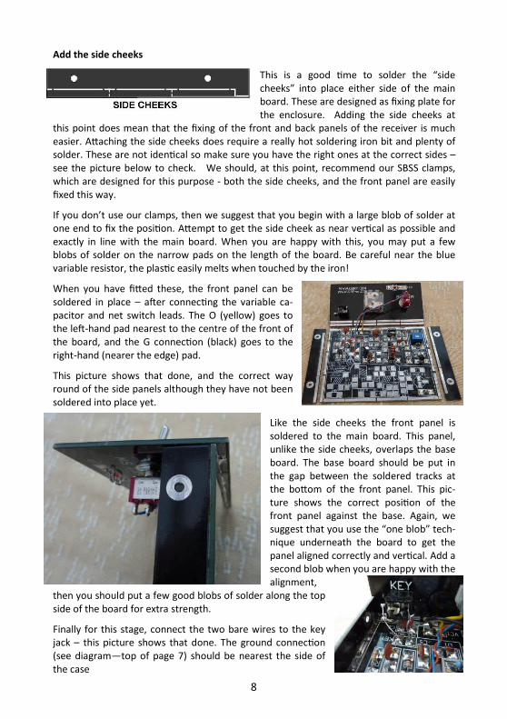
Add the side cheeks
This is a good 4me to solder the “side
cheeks” into place either side of the main
board. These are designed as fixing plate for
the enclosure. Adding the side cheeks at
this point does mean that the fixing of the front and back panels of the receiver is much
easier. A�aching the side cheeks does require a really hot soldering iron bit and plenty of
solder. These are not iden4cal so make sure you have the right ones at the correct sides –
see the picture below to check. We should, at this point, recommend our SBSS clamps,
which are designed for this purpose - both the side cheeks, and the front panel are easily
fixed this way.
If you don’t use our clamps, then we suggest that you begin with a large blob of solder at
one end to fix the posi4on. A�empt to get the side cheek as near ver4cal as possible and
exactly in line with the main board. When you are happy with this, you may put a few
blobs of solder on the narrow pads on the length of the board. Be careful near the blue
variable resistor, the plas4c easily melts when touched by the iron!
When you have fi�ed these, the front panel can be
soldered in place – a6er connec4ng the variable ca-
pacitor and net switch leads. The O (yellow) goes to
the le6-hand pad nearest to the centre of the front of
the board, and the G connec4on (black) goes to the
right-hand (nearer the edge) pad.
This picture shows that done, and the correct way
round of the side panels although they have not been
soldered into place yet.
Like the side cheeks the front panel is
soldered to the main board. This panel,
unlike the side cheeks, overlaps the base
board. The base board should be put in
the gap between the soldered tracks at
the bo�om of the front panel. This pic-
ture shows the correct posi4on of the
front panel against the base. Again, we
suggest that you use the “one blob” tech-
nique underneath the board to get the
panel aligned correctly and ver4cal. Add a
second blob when you are happy with the
alignment,
then you should put a few good blobs of solder along the top
side of the board for extra strength.
Finally for this stage, connect the two bare wires to the key
jack – this picture shows that done. The ground connec4on
(see diagram—top of page 7) should be nearest the side of
the case

9
Complete
circuit
diagram

10
Tes9ng the first sec9on
Tes4ng the transmi�er at this stage
requires a Diode Probe. All the parts
are provided for making such a probe as
shown in the picture.
The diode probe is built “Manha�an-
style” by a�aching a strip of five pads to
the top le6-hand corner of the printed
circuit board material using super glue.
The components are surface mounted as shown. The three le6-hand pads are joined using
an off-cut from one of the trimmed component leads.
Flexible wire in red, black, yellow and green is supplied. The yellow and green leads are
terminated with crocodile clips and the red and black leads are terminated with 4mm plugs
(the standard plug used in test meters). If your meter uses a different size of plug, then you
will have to obtain these yourself. The placement of the four leads is shown in the circuit
drawing. Later the diode probe will be converted into a basic wa�meter to measure the final
transmi�er output.
For those not familiar with 4mm plugs, the centre of the metal insert contains a grub screw
to secure the end of the wire. A small screw driver pushed up the centre of the metal insert
is used to clamp the end of the wire as shown. The metal insert is then pushed into the plas-
4c housing of the plug, wire being place in line with the slot in the plas4c housing. The insert
is now pushed un4l the end of the plug is as far out as it will travel. This does take force!
Pushing the end of the insert against a firm surface will help. You might need a screwdriver
to push in the final bit of the metal insert.
11
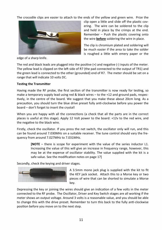
The crocodile clips are easier to a�ach to the ends of the yellow and green wire. Prize the
clip open a li�le and slide off the plas4c cov-
ering. The wire can be soldered to the clip
and held in place by the crimps at the end.
Remember – Push the plas4c covering onto
the wire before soldering the wire in place.
The clip is chromium plated and soldering will
be much easier if the area to take the solder
is roughed a li�le with emery paper or the
edge of a sharp knife.
The red and black leads are plugged into the posi4ve (+) and nega4ve (-) inputs of the meter.
The yellow lead is clipped on the le6 side of R7 (the pad connected to the output of TR1) and
the green lead is connected to the other (grounded) end of R7. The meter should be set on a
range that will indicate 10 volts DC.
Tes9ng the Transmi�er
Having made the RF probe, the first sec4on of the transmi�er is now ready for tes4ng, so
make a temporary supply lead using red & black wires – to the +12 and ground pads, respec-
4vely, in the centre of the board. We suggest that you make these about 20cm long. As a
precau4on, you should turn the blue drive preset fully an4-clockwise before you power the
board – don’t forget to insert the crystal!
When you are happy with all the connec4ons (a check that all the parts are in the correct
places is useful at this stage). Apply 12 Volt power to the board: +12v to the red wire, and
the nega4ve to the black wire.
Firstly, check the oscillator. If you press the net switch, the oscillator only will run, and this
can be found around 7.030MHz on a suitable receiver. The tune control should vary the fre-
quency from around 7.027MHz to 7.031MHz.
[NOTE – there is scope for experiment with the value of the series inductor L1.
Increasing the value of this will give an increase in frequency range, however, this
may be at the expense of oscillator stability. The value supplied with the kit is a
safe value. See the modifica4on notes on page 17]
Secondly, check the keying and driver stages.
A 3.5mm mono jack plug is supplied with the kit to fit
the KEY jack socket. A�ach this to a Morse key or two
pieces of wire that can be shorted to simulate a Morse
key.
Depressing the key or joining the wires should give an indica4on of a few volts in the meter
connected to the RF probe. The Oscillator, Driver and Key Switch stages are all working if the
meter shows an output voltage. Around 3 volts is a reasonable value, and you should be able
to change this with the drive preset. Remember to turn this back to the fully an4-clockwise
posi4on before you move on to the next step.

12
Now, the rest of the transmi�er.
The final amplifier
Firstly, wind the coil L2. This is 5 turns on a FT43-2402 binocular
toroid. Each turn goes through both holes of the core, and you
should end up with it looking like this.
It is helpful to insert this and the other components in the sec4on marked “FINAL” (ZD1,
R10, C6 and C7) before adding the final amplifier transistor (T3) (2N3866). ZD1 must be
connected the correct way round. The bo�om pad of the ZD1 placement shows a bar
marking; this corresponds to the bar (or ring) near one end of the zener diode.
Trim the transistor leads to about 10mm and bend the end 3mm of the transistor leads to
form a “foot” that will lay flush with the pads. The best direc4ons for the foot, assuming
the tab on the transistor case points upwards, are emi�er upwards, collector downwards
and base to the le6. Refer to the base connec4on diagram on the circuit schema4c. Using
pointed pliers manipulate the leads un4l each foot rests on the required pad. Tin the pads
and the leads and solder them in place. The heatsink is applied to the transistor by placing
a screwdriver blade in the gap and twis4ng it to open the vanes. The heatsink should now
fit over the transistor casing. The screwdriver is removed to allow the heatsink to clamp
firmly on the sides of the transistor.
The next step is to solder a 10cm length of yellow wire to the LED pad on the main board
(just to the rear of the +12v power pad, connect the other end of this to the LED pad on
the front panel. Tuck this wire in 4dily as you can see on the picture of the main board and
front panel below. The diodes D2 & D3 should be soldered into place - the diode D2/3 pads
have a bar marking (like ZD1) to show the way to mount them. Finally solder the “fat resis-
tor” sized inductor, L3 into place.
The low-pass filter
The low-pass filter coils (L4, L5 & L6) are wound on the yellow
cores using the gold wire. L4 and L6 have 21 turns, L5 has 20
turns. These require 14” (35cm) of wire for each coil. Wind as for
TR1 with one pass through the core being one turn. L5 has one
less turn (20) than L4 and L6 (21 each) so wind L5 first and lay it
aside so that it won’t be confused with the others. 35cm of wire
is easily enough for each coil. The windings on each core should
occupy about three-quarters of the circumference.

13
Nearly all the capacitors in the filter are actually two in parallel as the
correct values are not commercially available. We suggest that you paral-
lel these pairs first as shown here, before fiGng them. A good plan is to
mount C12 - C15, and C18, then mount L5, followed by L4 and L6.
Here is a picture of the completed
board so far.
The layout of the printed circuit
board. This shows the wiring be-
tween the pads

14
The back panel.
Firstly, mount the three sockets on the back panel – the antenna socket, the receiver aerial
socket and the power socket.
The antenna sockets
The antenna socket (ANT) is a single hole fixing
phono socket, as is the RECEIVER socket. These
require two wires to be joined to the ANT pads on
the main board and we will connect these in a
moment.
The power socket
The POWER socket also has two connec4ons that connect to the
main board and it is vital to get these the correct way round. Again,
we will connect these shortly.
The receiver mu9ng
The components for the receiver mu4ng sec4on are mounted inside the back panel, and
you should now fit these. Solder the resistors into place first, followed by the transistors. It
is best to keep the lead length of these parts short if possible.
The next job is to connect the rear panel to main board. Firstly, you need to cut seven
lengths of wire. The first three are on the back panel and are as follows:
RCVR on the back panel connects to the centre of the RECEIVER phono socket – use
3cm of orange wire for this.
GND on the back panel connects to the ground tag on the RECEIVER phono socket –
use 1½cm of bare wire for this.
Solder a 10cm length of red wire to the +12 tag on the back panel but do not connect
the other end yet.
Now cut the other four pieces as follows and solder these to the pads on the main board:
R-MUTE on the main board – use a 9cm length of green wire for this.
K-MUTE on the (bo�om of club logo) on the main board – use a 10cm length of or-
ange wire for this.
ANT on the main board – use two 9cm lengths of wire – black and blue, the black
(ground) connec4on goes to the le6-hand pad and the blue (antenna connec-
4on) goes to the right-hand pad. Y
You should already have two pieces of wire connected to the +12V and GND tags of
the main board that we used for tes4ng. Cut these to 9cm long.
15
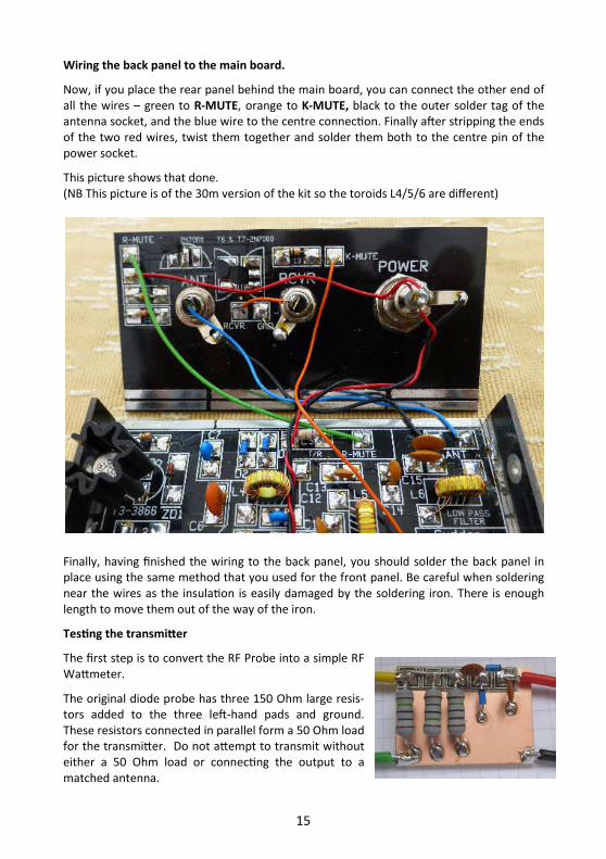
Wiring the back panel to the main board.
Now, if you place the rear panel behind the main board, you can connect the other end of
all the wires – green to R-MUTE, orange to K-MUTE, black to the outer solder tag of the
antenna socket, and the blue wire to the centre connec4on. Finally a6er stripping the ends
of the two red wires, twist them together and solder them both to the centre pin of the
power socket.
This picture shows that done.
(NB This picture is of the 30m version of the kit so the toroids L4/5/6 are different)
Finally, having finished the wiring to the back panel, you should solder the back panel in
place using the same method that you used for the front panel. Be careful when soldering
near the wires as the insula4on is easily damaged by the soldering iron. There is enough
length to move them out of the way of the iron.
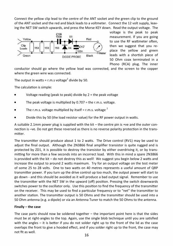
Tes9ng the transmi�er
The first step is to convert the RF Probe into a simple RF
Wa�meter.
The original diode probe has three 150 Ohm large resis-
tors added to the three le6-hand pads and ground.
These resistors connected in parallel form a 50 Ohm load
for the transmi�er. Do not a�empt to transmit without
either a 50 Ohm load or connec4ng the output to a
matched antenna.
16
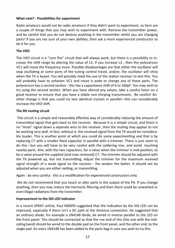
Connect the yellow clip lead to the centre of the ANT socket and the green clip to the ground
of the ANT socket and the red and black leads to a voltmeter. Connect the 12 volt supply, leav-
ing the NET SW switch upwards, and press the Morse KEY down. Read the output voltage. The
voltage is the peak to peak
measurement. If you are going
to use the RF wa�meter o6en,
then we suggest that you re-
place the yellow and green
leads with a shor4sh piece of
50 Ohm coax terminated in a
Phono (RCA) plug. The inner
conductor should go where the yellow lead was connected, and the screen to the copper
where the green wire was connected.
The output in wa�s = r.m.s voltage2 divide by 50.
The calcula4on is simple:
• Voltage reading (peak to peak) divide by 2 = the peak voltage
• The peak voltage is mul4plied by 0.707 = the r.m.s. voltage.
• The r.m.s. voltage mul4plied by itself = r.m.s. voltage 2
• Divide this by 50 (the load resistor value) for the RF power output in wa�s.
A suitable 2.1mm power plug is supplied with the kit – the centre pin is +ve and the outer con-
nec4on is –ve. Do not get these reversed as there is no reverse polarity protec4on in the trans-
mi�er.
The transmi�er should produce about 1 to 2 wa�s. The Drive control (RV1) may be used to
adjust the final output. Although the 2N3866 final amplifier transistor is quite rugged and is
protected by ZD1, it is possible to destroy the transistor by either overdriving it, or by trans-
miGng for more than a few seconds into an incorrect load. With this in mind a spare 2N3866
is provided with the kit – do not destroy this as well! We suggest you begin below 2 wa�s and
increase the output to around 2 wa�s maximum. Try for an output voltage on the test meter
of some 25 to 28 volts. One to two wa�s on 40 metres represents a useful amount of QRP
transmi�er power. If you turn up the drive control up too much, the output power will start to
go down - and this should be avoided as it will produce a bad output signal. Remember to use
the transmi�er with the NET SW in the upward (off) posi4on. Pressing the switch downwards
switches power to the oscillator only. Use this posi4on to find the frequency of the transmi�er
on the receiver. This may be used to find a par4cular frequency or to “net” the transmi�er to
another sta4on. The transmi�er output is 50 Ohms and the transmi�er should be used into a
50 Ohm antenna (e.g. a dipole) or via an Antenna Tuner to match the 50 Ohms to the antenna.
Finally – the case
The case parts should now be soldered together – the important point here is that the sides
must be at right-angles to the top. Again, use the single blob technique un4l you are sa4sfied
with the angles – it is be�er if you do not solder right up to the front of the lid as the case
overlaps the front to give a hooded effect, and if you solder right up to the front, the case may
not fit as well.
17
What next? - Possibili9es for experiment
Radio amateurs would not be radio amateurs if they didn't want to experiment, so here are
a couple of things that you may wish to experiment with. Remove the transmi�er power,
and be careful that you do not destroy anything in the transmi�er whilst you are changing
parts! If you are not sure of your own abili4es, then ask a more experienced constructor to
do it for you.
The VXO
The VXO circuit is a “sure fire” circuit that will always work, but there is a possibility to in-
crease the shi6 range by altering the value of L3. If you increase L3 , then the polyvaricon
VC1 will move the frequency more. Possible disadvantages are that either the oscillator will
stop oscilla4ng at some parts of the tuning control travel, and/or, the oscillator will chirp
when the TX is keyed. You will possibly need the use of the sta4on receiver to test this. You
will probably have to unfasten VC1 and move it aside to change any of these parts. The
polyvaricon has a second sec4on - this has a capacitance shi6 of 6 to 160pF. You may wish to
try using the second sec4on. When you have altered any values, take a careful listen on a
good receiver to ensure that you have a stable non-chirping transmission. Be careful! An-
other change is that you could try two iden4cal crystals in parallel—this can considerably
increase the VXO shi6.
The RX mu9ng circuit
This circuit is a simple and reasonably effec4ve way of considerably reducing the amount of
transmi�ed signal that gets back to the receiver. Because it is a simple circuit, and there is
no “mute” signal down a separate wire to the receiver, then the mu4ng may appear to not
be working very well. In fact, without it, the received signal from the TX would be considera-
bly louder. This is another point at which you could do some experimen4ng and that is by
replacing C7 with a smaller fixed capacitor in parallel with a trimmer. There is just room to
do this—but you will have to be very careful with the soldering iron, and avoid touching
nearby parts. Aim, with the two capacitors, for a value when the trimmer is mid-posi4on, to
be a value around the supplied (and now removed) C7. The trimmer should be adjusted with
the TX powered up, but not transmiGng. Adjust the trimmer for the maximum received
signal strength of a weak signal on the receiver - the weaker the be�er. It should not be
adjusted when you are either neGng, or transmiGng.
Again - be very careful - this is a modifica4on for experienced constructors only.
We do not recommend that you touch or alter parts in the output of the PA. If you change
anything, then you may reduce the harmonic filtering and then there could be unwanted or
even illegal radia4ons from the transmi�er.
Improvement to the SIG LED indicator
in a recent SPRAT ar4cle, Paul M0XPD suggested that the indica4on by the SIG LED can be
improved, especially if there isn’t a DC path at the Antenna connec4on. He suggested that
an ordinary diode, for example a 1N4148 diode, be wired in inverse parallel to the LED on
the front panel. This should be connected so that the +ve end of this (the one with the indi-
ca4ng band) should be wired to the double pad on the front panel, and the other end, to the
single pad. An extra 1N4148 has been added to the parts bag in case you wish to try this.

18
Value Markings Resistors
R1 47k Yellow, purple, orange, gold R2 470 Yellow, purple, brown, gold R3 120 Brown, red, black, black, brown R4 2k2 Red, red, red, gold R5 470 Yellow, purple, brown, gold R6 10 Brown, black, black, gold R7 33 Orange, orange, black, gold R8 1k Brown, black, red, gold R9 47k Yellow, purple, orange, gold R10 1k Brown, black, red, gold R11 2k2 Red, red, red, gold R12 10k Brown, black, orange, gold R13 10k Brown, black, orange, gold R14 150 Brown, green, black, black, brown R15 150 Brown, green, black, black, brown R16 150 Brown, green, black, black, brown
Capacitors
C1 100nF 104 C2 47pF 47 C3 100pF 101 C4 47pF 47 C5 100nF 104 C6 100nF 104 C7 47pF 47 C8 100nF 104 C9 100nF 104 C10 100nF 104 C11 10uF 10uF (the –ve side is plainly marked) C12 377pF (330 + 47pF) * 331 + 47 C13 660pF (330 + 330pF) * 331 + 331 C14 660pF (330 + 330pF) * 331 + 331 C15 430pF (330 + 100pF) * 331 + 101
C16 & 17 2 x 100nF 104 (for RF probe) C18 100pF 101
* these values are 2 capacitors in parallel – see text
Inductors L1 10uH Brown, black, black, silver L2 BN43-2402 binocular core Pig nose – 5 complete turns 30SWG L3 10uH Brown, black, black, silver L4 T37-6 Yellow/black – 21 turns L5 T37-6 Yellow/black – 20 turns L6 T37-6 Yellow/black – 21 turns
TR1 FT37-43 Black – 25t (30SWG) + 5t (27SWG)
19
Other parts RV1 50 Ohm Drive control preset VC1 60pF Tuning SW miniature toggle switch Net switch (may be a 2 tag part) J1 3.5mm mono jack socket Key jack J2 Phono/RCA socket Antenna J3 Phono/RCA socket Antenna to receiver X1 Crystal 7.030MHz HC49U wire lead crystal
Socket Crystal socket 3 SIL sockets 35mm knob For VXO tuning capacitor
Magnet wire 30 SWG Gold coloured Magnet wire 27 SWG Red coloured
PVC wire 6 colours of wire Red, Black, Orange, Yellow, Blue & Green Heatsink For PA transistor
Power socket Panel mounting 2.1mm Power plug 2.1mm
4 feet for case Key plug 3.5mm mono plug
Blank PCB For probe 5 MEsquares For probe Extra flex wire For probe Black, Red, Yellow, Green
4mm plugs For probe Black, Red Min crocodile clips For probe Yellow, Green
LED Output indicator ZD1 33v zener diode (BZX55C33) PA protector
D2 1N5711 RX parallel mute D3 1N5711 RX parallel mute D4 1N5711 Probe detector D5 1N5711 Probe detector
D1 1N4148 For net switch T7 2N7000 RX parallel mute
Semiconductors
T1 2N3904 Oscillator T2 2N3904 Driver T3 2N3866 (4-247 CG9949) PA (spare included)
T5 2N7000 RX series mute T6 2N7000 voltage inverter
T4 2N3906 Keyer
Toroids For L4, L5 & L6 3 x T37-6 - yellow/black
Toroid For T1 FT37-43 - black Pig-nose toroid For L2 BN43-2402
Screws 4 off self-tapping screws For fixing the case to the base
Extra diode 1N4148 This is a second diode in case you wish to try the SIG LED indicator improvement (see
20
The finished transmi�er
NB - this is a picture of the 30m version of the kit
© G-QRP Club 2010/11/12/13/14/15/16
V2.8 September 2016