

The Failure Analysis Process - ASM International
15
The Failure Analysis Process M. Steven Ferrier Metatech Corporation 1190 SW Sunset Drive Corvallis, OR 97333 Telephone 541-752-2713 Email [email protected] Introduction. How does an experienced Failure Analysis engineer crack a tough analysis? What makes the difference between a new engineer's Fail- ure Analysis approach and the seasoned, effective analysis method of a veteran? Can our industry cap- ture a formulation of correct Failure Analysis meth- odology to accelerate the development of new engi- neers and aid the strong skills of experienced ana- lysts? More crucial, perhaps, is the underlying question, Are we able as analysts to think abstractly about the nature of our work? Or are we instead bound to a tool-focused, concrete way of thinking that has all the adaptability of the construction material of the same name? While our historical inability in the FA indus- try to abstract a general process from our daily work will probably not doom our discipline, this shortcom- ing will certainly rob us of a great deal of efficiency, flexibility and basic understanding of what we do in electronic device Failure Analysis. This author has the conviction that we are a better group of people than to allow this shortcoming to continue undetected and uncorrected for much longer. While many or most Failure Analysis departments make the definition and application of specific analy- sis process flows a significant priority, the subject of general FA methodology remains a minor one in the literature as of this writing. 1-3 By way of a summary remediation, this tutorial paper presents a fully-gen- eral analysis formalization intended to make the fail- ure analysis design efficient, rigorous and consistent from analysis to analysis and from failure to failure. The formalization amounts to a practical form of sci- entific method 4,5 , customized for the failure analysis discipline, and enabling faster analysis to satisfy business constraints. The analysis design methodology, or decision en- gine, can be formulated as six steps arranged in a cy- cle or loop, shown in Fig. 1. This may not look like a Failure Analysis process flow, which is appropriate, since it is not, strictly speaking, such a flow. Instead, these steps in this order form a metaprocess, that is, a process whose function is to create another process. Applied to semiconductor failure analysis, this gen- eral decision engine metaprocess creates a specific analysis flow for a specific failure based on the facts about the failure, the results of analysis operations, the body of knowledge about physical causes and their effects and, finally, inferential logic. This metaprocess is intended to work properly—that is, generate a correct unique failure analysis flow—for any failure analysis of a manufactured product com- ing from any of the semiconductor wafer and pack- aging processes predominant today. Using the ap- proach described in this tutorial, the analyst of any experience level should become able to make analy- sis choices in ways that reflect mature failure analysis skills. This approach can thus accelerate the maturity Figure 1 Scientific Method Metaprocess Loop for Failure Analysis (unfolded version) Construct an existence-correlation-causation ques- tion (E/C/C Question) Make a measurement to address that question (Measurement) Interpret the results of the measurement to answer the E/C/C Question (Interpretation) Cast the answer in an existence-correlation- causation form (E/C/C Answer) Build a correlation list of possible prior causes and their effects (Correlation List) Select one or more items from the List about which to construct a new E/C/C Question (Selection) Measurement E/C/C Question E/C/C Answer Correlation List (start of next loop) Interpretation Selection (end of prior loop) Microelectronics Failure Analysis Desk Reference, Sixth Edition R.J. Ross, editor Copyright © 2011 ASM International®. All rights reserved. Product code: 09110Z 1
Transcript of The Failure Analysis Process - ASM International

The Failure Analysis Process M. Steven Ferrier
Metatech Corporation � 1190 SW Sunset Drive � Corvallis, OR 97333 Telephone 541-752-2713 � Email [email protected]
Introduction. How does an experienced Failure Analysis engineer crack a tough analysis? What makes the difference between a new engineer's Fail-ure Analysis approach and the seasoned, effective analysis method of a veteran? Can our industry cap-ture a formulation of correct Failure Analysis meth-odology to accelerate the development of new engi-neers and aid the strong skills of experienced ana-lysts?
More crucial, perhaps, is the underlying question, Are we able as analysts to think abstractly about the nature of our work? Or are we instead bound to a tool-focused, concrete way of thinking that has all the adaptability of the construction material of the same name? While our historical inability in the FA indus-try to abstract a general process from our daily work will probably not doom our discipline, this shortcom-ing will certainly rob us of a great deal of efficiency, flexibility and basic understanding of what we do in electronic device Failure Analysis. This author has the conviction that we are a better group of people than to allow this shortcoming to continue undetected and uncorrected for much longer.
While many or most Failure Analysis departments make the definition and application of specific analy-sis process flows a significant priority, the subject of general FA methodology remains a minor one in the literature as of this writing.1-3 By way of a summary remediation, this tutorial paper presents a fully-gen-
eral analysis formalization intended to make the fail-ure analysis design efficient, rigorous and consistent from analysis to analysis and from failure to failure. The formalization amounts to a practical form of sci-entific method4,5, customized for the failure analysis discipline, and enabling faster analysis to satisfy business constraints.
The analysis design methodology, or decision en-gine, can be formulated as six steps arranged in a cy-cle or loop, shown in Fig. 1. This may not look like a Failure Analysis process flow, which is appropriate, since it is not, strictly speaking, such a flow. Instead, these steps in this order form a metaprocess, that is, a process whose function is to create another process. Applied to semiconductor failure analysis, this gen-eral decision engine metaprocess creates a specific analysis flow for a specific failure based on the facts about the failure, the results of analysis operations, the body of knowledge about physical causes and their effects and, finally, inferential logic. This metaprocess is intended to work properly—that is, generate a correct unique failure analysis flow—for any failure analysis of a manufactured product com-ing from any of the semiconductor wafer and pack-aging processes predominant today. Using the ap-proach described in this tutorial, the analyst of any experience level should become able to make analy-sis choices in ways that reflect mature failure analysis skills. This approach can thus accelerate the maturity
Figure 1 Scientific Method Metaprocess Loop for Failure Analysis (unfolded version)
Construct an existence-correlation-causation ques-tion (E/C/C Question)
Make a measurement to address that question (Measurement)
Interpret the results of the measurement to answer the E/C/C Question (Interpretation)
Cast the answer in an existence-correlation-causation form (E/C/C Answer)
Build a correlation list of possible prior causes and their effects (Correlation List)
Select one or more items from the List about which to construct a new E/C/C Question (Selection)
Measurement
E/C/C Question
E/C/C Answer
Correlation List
(start of next loop)
Interpretation
Selection
(end of prior loop)
Microelectronics Failure AnalysisDesk Reference, Sixth Edition R.J. Ross, editor
Copyright © 2011 ASM International®.All rights reserved.
Product code: 09110Z
1

of beginning analysts once they have the small amount of experience needed to use the metaprocess effectively. Some benefits of this methodology will be described in detail a little later in the tutorial. All examples of any kind in this tutorial, with one major exception described shortly, are hypothetical but pos-sible.
The Metaprocess in a Nutshell. Very briefly, here is how this metaprocess produces a correct de-vice analysis flow. All analysis starts with under-standing the failure mode. We have a part and a complaint; does the failure mode exist on this part and match the complaint? We make a measurement to confirm the failure mode. If we do confirm the mode, it makes sense, rather than just jumping into a measurement, to ask ourselves what could cause the mode. Even if we have no data yet, we can still come up with a list of possible causes that may be substan-tial. The next step is to write down on our list other effects of the causes we just wrote down on our list. We then select one effect on our list and ask whether it exists.
The reader will notice that at this point we are back where we started: asking whether an effect ex-ists. We began by asking whether the effect called the failure mode exists, and ended by asking whether an effect on our list existed. This makes it clear that the pro??cess we are using represents a loop. If we follow this loop, it will lead us from the failure mode to the root anomaly. Pursuing a rigorous version of this approach provides the correct analysis flow.
The Metaprocess in Real Life. To show this, we start with a real-life example of the use of this ap-proach, drawn verbatim (excepting a few editorial excisions) from a published ISTFA paper6. After this practical example, we will provide some clear defini-tions of basic terms and then proceed to explain the six steps on their own merits.
Application of a formal Failure Analysis meta-process to a stubborn yield loss problem provided a framework that ultimately facilitated a solution. Ab-sence of results from conventional failure analysis techniques such as PEM (Photon Emission Mi-croscopy) and liquid crystal microthermography frus-trated early attempts to analyze this low-level supply leakage failure mode. Subsequently, a reorganized analysis team attacked the problem using a specific top-level metaprocessa,4.
Using the metaprocess, analysts generated a spe-cific unique step-by-step analysis process in real time. Along the way, this approach encouraged the creative identification of secondary failure effects that provided repeated breakthroughs in the analysis flow. Analysis proceeded steadily toward the failure cause in spite of its character as a three-way interac-tion among factors in the IC design, mask generation, and wafer manufacturing processes. The metaprocess
a A metaprocess is a general process whose pur-pose and function is to create a specific process to suit specific conditions and requirements.
also provided the formal structure that, at the conclu-sion of the analysis, permitted a one-sheet summary of the failure's cause-effect relationships and the analysis flow leading to discovery of the anomaly.
As with every application of this metaprocess, the resulting analysis flow simply represented an effec-tive version of good failure analysis. The formal and flexible codification of the analysis decision-making process, however, provided several specific benefits, not least of which was the ability to proceed with high confidence that the problem could and would be solved. This tutorial describes the application of the metaprocess, and also the key measurements and cause-effect relationships in the analysis.
Manufacturing and Failure Mode. The yield failure mode, labeled VDD Leakage, occurred in a specific printhead IC manufactured in a 1.0 um sin-gle-poly three-metal CMOS process. Although this is a relatively simple wafer process, the mode's charac-teristics conspired to counteract any real benefit from the process simplicity. Up to 80% of the IC's manu-factured exhibited a slightly elevated (but definitely anomalous) supply leakage current in a standby con-
Figure 3 Cumulative distribution of leakage behavior of related but non-failing design with IDD of over 90% of devices falling below 200nA.
Figure 2 Cumulative distribution of failing design leakage behavior of wafer lots with only 20% of IDD currents falling below 200nA.
2

figuration compared to comparable IC designs. The anomalous leakage current revealed itself as a sloppy cumulative current distribution curve (Fig. 2) com-pared to the clean curves of non-failing designs (Fig. 3).
Another fact stood out at the outset as a clear clue. The leakage did not occur on the susceptible design when it was manufactured in an older wafer process with significantly heavier n-well doping. Early fail-ure analysis indicated no correlating liquid-crystal transitions, a result consistent with the leakage levels of approximately 1-5uA. Other traditional analysis measurements (including a search for correlating photon emission) also proved unsuccessful. In spite of months of yield loss without a resolution, the team responsible for yield refused on principle to simply raise the test limit and redefine this product as 'good'.
Application of the Metaprocess. The problem was eventually returned to the IC's designers, and a task force assembled across design and manufactur-ing organizations to solve the problem. The ensuing analysis was guided chiefly by a cyclic metaprocess, diagrammed in Fig. 1 above. This metaprocess per-formed a critical three functions for the analysis ef-fort.
Function 1. The metaprocess provided a constant focus on (a) the nature and details of the cause-effect network that the failure had created, (b) the analysis path, and (c) the location (status) of current analysis activity on that path. The metaprocess provided this function through the canonical form of the E/C/C Question, "Does <the selected specific possible prior cause> Exist, Correlate with <the known, observed failing behavior>, and Cause that behavior? For ex-ample, at one point the question became: "Does the possible gate oxide short exist, correlate with the known quadratic IDD leakage, and cause that leak-age?" Depending upon the answer to this question, one of the following three cases applied:
I. The analysis path is false (in this example, the possible cause, a gate short, did not exist);
II. The analysis path is near the main cause-effect relationship (the possible cause, a gate short, existed and correlated with the observed quadratic IDD be-havior);
III. The analysis path is at the main cause-effect relationship (the possible cause, a gate short, existed, correlated with the known IDD behavior, and was re-lated to the behavior as cause and effect by a specific physical law of transistor operation).
Function 2. The metaprocess directed focus evenly on both halves of any good analysis: meas-urement and prior cause postulation. The former tempts many analysts to neglect to focus on possible prior causes. The Correlation List step (middle bot-tom) forced consideration of possible causes for the observed behavior, and then focused analysis meas-urement design to the goal of detecting secondary or side effects of those possible causes5. This repeat-edly drove innovation and inspired creative analysis approaches. Conversely, the Measurement step
(middle top) disciplined the construction of the Cor-relation List to treat possible prior causes arising from the failure's anomalous behavior rather than from speculation.
Function 3. The metaprocess provided applica-tion points for methodical analysis logic. At some points during analysis, behavior that correlated with failure differed very little from behavior that did not. The metaprocess facilitated the use of logical princi-ples able to accurately distinguish fine differences, such as the Contrapositive Testb and Inductive Proofc.
Analysis Flow. The following section describes the overall analysis flow arising from the metapro-cess, including some details of its application.
A. Failure Mode Verification and Characteriza-tion. In verifying failure mode, analysis began with a focus on the causes and effects operating in the fail-ing IC, incorporating the first function informed by the metaprocess described earlier (providing a con-stant focus on the nature and details of the cause-ef-fect failure-created network, the analysis path, and the location of current analysis activity on that path). The metaprocess loop was initiated, as Fig. 1 indi-cates, at the E/C/C Question step.
E/C/C Question: Does the reported VDD leakage exist, correlate with the complaint, and cause this IC to be categorized as a failure?
Measurement: Under conditions matching the failed test, the die under analysis exhibited anoma-
lous IDD(VDD,T) current (Fig. 4). Interpretation: Voltage and temperature behavior
of the anomalous current matched the complaint be-havior.
b Contrapositive Test: The test of a statement P by seeking a valid consequent Q that is false. P=>Q means that any ~Q=>~P. In FA terms, if a sure effect is truly absent, its cause is absent.
c Inductive Proof: The proof of a statement P by sufficient demonstration of valid and true conse-quents Qn without exception: for n>sufficient limit, P=>Qn and all Qn are found true. In FA terms, if the first predicted side effect is present, test for the next. If sufficient side effects are present without excep-tion, declare the common cause of all side effects proved and therefore present.
Figure 4 IDD(VDD,T) for a failing IC, with a superim-posed flat 1.0uA test limit surface.
3
E/C/C Answer: VDD leakage existed, correlated with the complaint, and caused the IC to be catego-rized as a failure.
B. Analysis Flow Generated by the Metaprocess. The main part of the analysis follows. After the E/C/C Answer that validated the failure mode, a Cor-relation List was next constructed. This step ad-dressed two (non-E/C/C) questions:
1. What possible prior causes may create the con-firmed VDD leakage?
2. What other effects do each of these possible prior causes imply?
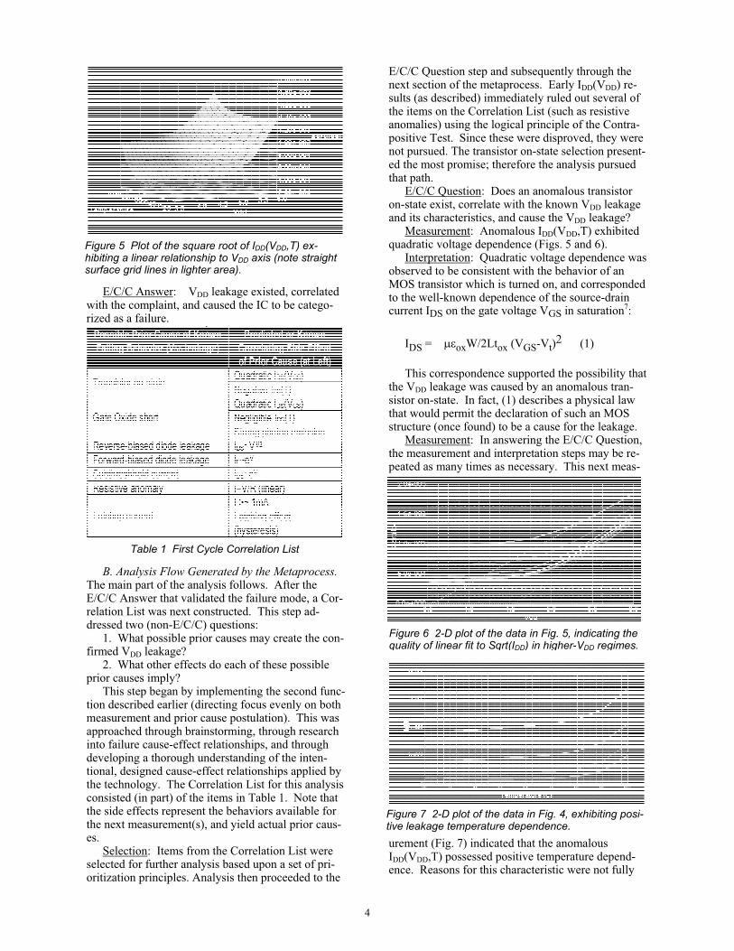
This step began by implementing the second func-tion described earlier (directing focus evenly on both measurement and prior cause postulation). This was approached through brainstorming, through research into failure cause-effect relationships, and through developing a thorough understanding of the inten-tional, designed cause-effect relationships applied by the technology. The Correlation List for this analysis consisted (in part) of the items in Table 1. Note that the side effects represent the behaviors available for the next measurement(s), and yield actual prior caus-es.
Selection: Items from the Correlation List were selected for further analysis based upon a set of pri-oritization principles. Analysis then proceeded to the
E/C/C Question step and subsequently through the next section of the metaprocess. Early IDD(VDD) re-sults (as described) immediately ruled out several of the items on the Correlation List (such as resistive anomalies) using the logical principle of the Contra-positive Test. Since these were disproved, they were not pursued. The transistor on-state selection present-ed the most promise; therefore the analysis pursued that path.
E/C/C Question: Does an anomalous transistor on-state exist, correlate with the known VDD leakage and its characteristics, and cause the VDD leakage?
Measurement: Anomalous IDD(VDD,T) exhibited quadratic voltage dependence (Figs. 5 and 6).
Interpretation: Quadratic voltage dependence was observed to be consistent with the behavior of an MOS transistor which is turned on, and corresponded to the well-known dependence of the source-drain current IDS on the gate voltage VGS in saturation7:
IDS = ��oxW/2Ltox (VGS-Vt)2 (1) This correspondence supported the possibility that
the VDD leakage was caused by an anomalous tran-sistor on-state. In fact, (1) describes a physical law that would permit the declaration of such an MOS structure (once found) to be a cause for the leakage.
Measurement: In answering the E/C/C Question, the measurement and interpretation steps may be re-peated as many times as necessary. This next meas-
urement (Fig. 7) indicated that the anomalous IDD(VDD,T) possessed positive temperature depend-ence. Reasons for this characteristic were not fully
Figure 5 Plot of the square root of IDD(VDD,T) ex-hibiting a linear relationship to VDD axis (note straight surface grid lines in lighter area).
Figure 7 2-D plot of the data in Fig. 4, exhibiting posi-tive leakage temperature dependence.
Figure 6 2-D plot of the data in Fig. 5, indicating the quality of linear fit to Sqrt(IDD) in higher-VDD regimes.
Table 1 First Cycle Correlation List
4

apparent during this phase of the analysis, but possi-ble explanations arose near the end of the analysis from the observed root anomaly. Even more impor-tantly in the short term, this characteristic helped lo-calize the failure site (described shortly).
Interpretation: This observed temperature behav-ior was the opposite of that expected from a transis-tor. Normally, channel mobility �, which dominates8 the temperature dependence of the saturated MOS drain current ID, decreases with increasing tempera-ture9. Therefore, the structure that was causing the anomalous current to flow should not be solely an MOS transistor. Nonetheless, the quadratic I(V) be-havior represented an indicator of MOS transistor in-volvement that could not be dismissed. This conflict was resolved by postulating a structure that included an MOS transistor, but also incorporated other com-ponents whose temperature dependence dominated that of the transistor. Such a structure could be pos-tulated while leaving its particular components un-specified for the moment.
Measurement: Next, a new photon emission mea-surement was performed, which again exhibited no emission signal, even at higher voltages and tempera-tures that significantly increased the failing VDD leak-age.
Interpretation: System tests verified that the PEM systems used in these measurements were capable of detecting emission from forward-biased diode struc-tures passing currents in the single-digit microampere range.
Recombination rates of MOS transistors were ex-pected to fall below this range, and therefore any such emission would remain undetected. This nega-tive result did, however, definitively rule out a gate oxide short (whose stronger emission should have been detected). The logical principle of the Contra-positive Test immediately demanded this conclusion.
E/C/C Answer: A circuit anomaly that includes a transistor on-state exists, correlates with the con-firmed VDD leakage, and causes it.
Correlation List: The Correlation List (Table 2) was next constructed. This list contains possible pri-or causes for the just-confirmed behavior (the anoma-lous transistor on-state), and also includes other side effects (effects other than observed VDD leakage) of those possible prior causes. In clarification of the re-set signal entry noted in Table 2, it was known from earlier work that the external reset pin could turn off the leakage on failing dice, which led to the reset state as a possible prior cause in the electrical do-main. The Table also includes normal transistors in an abnormal on state due to abnormal electrical con-ditions, as well as abnormal (unintended) transistors.
Selection: The correlation of the reset pin state with the observed VDD leakage was selected. This prior cause postulated that the test, which was expect-ed to set the reset pin to an active state, actually set it to an inactive state thereby allowing the leakage to occur.
In order to summarize the next several
metaprocess steps, an E/C/C Question was framed concerning the selected PPC (Possible Prior Cause); that is, the reset pin state's correlation to the leakage: does an incorrect reset condition exist, correlate with the leakage, and cause it? Following this, a meas-urement determined that the normal reset state (rather than the incorrect state) correlated with leakage. This ruled out incorrect reset pin setup during testing and, in terms of the E/C/C Answer, that this possible prior cause did not exist. (Note that this did not mean that the correlation of the reset pin state to the failure was ignored, but rather that a test error creating the leak-age by an incorrect reset pin state was ruled out.)
From the metaprocess flow, the next step would be to make a new selection from the same Correlation List since the prior cause of the same known effect was still under examination. In order to pursue the remaining Correlation List items (as described), how-ever, it was necessary to resolve the question of ex-actly which structure was causing the leakage.
The most important methodology question at this stage in any analysis is: how can more information about the cause-effect relationships involved in the failure be obtained? This question drives the most challenging and significant operation within typical analysis flows: localization. Localization is valued as the only effective way to gather extensive informa-tion about the effects created by a defect. The ulti-mate purpose of localization is to provide greater ac-cess to the cause-effect network immediately sur-rounding the defect.
During a localization operation, the analysis makes no progress down the cause-effect chain. In-stead, the analyst spends time and effort working to place the known failure behavior characteristics at some location in the IC's physical structure. This means that the analysis remains at the same point in the cause-effect chain while the spatial correlation of the failure's known behavior is identified.
In this case, PEM and Liquid Crystal provided no signals for localization. The IC was too complex to perform electrical localization in the design's own cause-effect domains (blocks' effects on other blocks), and the network of metallization was too dense to easily permit Focused Ion Beam (FIB) cut localization of the leakage path (from the topmost die level).
The discipline imposed by the Correlation List step (demanding enumeration of all possible secon-dary effects of the possible prior causes) yielded a re-turn at this point. The leakage's positive temperature coefficient (Figs. 5-7) should be local to the anomaly site. The analysts therefore sought to locate this characteristic in the die interior.
E/C/C Question: Does a local thermal effect ex-ist, correlate with the observed global IDD tempera-ture characteristics, and cause them? With this ques-tion in mind, a local heater was built. Its tip diameter (defining its spatial resolution) was large at 1000 um, but this still represented a relatively small region of the IC.
5

Measurement: Using the topside airflow heater, a topside temperature rise was impressed at various points across the IC, and a very slight rise in IDD leakage as a function of the heater position was ob-served. Considerable effort was required to separate the signal from the noise, and only a few data points per day resulted.
Interpretation: Although not all regions were ex-amined due to the laborious process involved, results obtained suggested that approximately 90% of the IC area could be ignored, and that the analysis could fo-cus on a relatively small region at the top of the die. A plot of the signal as a function of die location ap-pears in Fig. 8. The region at the left of the figure is at the top of the die. This interpretation confirmed
that the effect named in the Correlation List (Table 2), a localized IDD(T,x,y), did exist and correlated with the global failure behavior. Since no physical law demanded that this thermal characteristic caused the observed leakage, only the first two sub-questions could be answered positively for this possible prior cause.
E/C/C Answer: A local thermal effect exists, cor-
relates with the failure behavior, but does not cause it.
Since an effect (but not the prior cause itself) had been localized, the next step was to revisit or recon-struct the Correlation List. To proceed effectively at this point, however, improved access to the cause-ef-fect network around the specific defect or anomaly was needed. To gain this access, material was built using a custom metal mask. Failing wafers built with this mask routed their (anomalous) supply current through a middle metallization sandwich layer. A FIB cut then confirmed the thermal map's results. A typical cycle through the metaprocess took shape as
described next. Correlation List: Localization can be executed
without much elaboration. It should be understood and developed, however, as a series of loops through the Fig. 1 metaprocess. To enable this, the Correla-tion List indicated in Table 3 was constructed. Lo-calization then continued based upon the Correlation List items identified.
Selection: IDD current path in analog circuitry section.
E/C/C Question: Does a current path in the ana-log circuitry section exist, correlate with global fail-ure characteristics, and cause them?
Measurement: All but the bottom (more resistive) refractory metal layer was removed mechanically (by probe scrub) and measurements made for possible re-sulting voltage drops.
Interpretation: Results exhibited no voltage drops along any VDD metallization path to the analog cir-cuitry.
Measurement: Focused Ion Beam (FIB) cuts iso-
Table 2 Second Cycle Correlation List
Figure 8 ��IDD(x,y) generated by topside heating
Table 3 Final correlation list related to observed anomaly
6

lated current paths between the external VDD pin and analog circuitry. Global IDD was then re-measured.
Interpretation: External current exhibited original characteristics as a function of voltage (anomalous current was not eliminated by the FIB cut).
E/C/C Answer: A current path in the analog cir-cuitry does not exist.
At this point, current localization was pursued on multiple devices by FIB and other means until it was traced, first to a region of standard cells, then to a half-row within the region, and finally to two similar standard cells in the row (Fig. 9). This region was broadly consistent with the thermal map in Fig. 8. Correlation of the two cells to the leakage was dem-onstrated by tying the local implementation of the re-set line of each cell to the low-current state. These
FIB modifications produced approximately a 50% re-duction of the anomalous IDD leakage for each cell. To further localize the current path, the local reset within the cell was isolated before and after an in-verter, and the post-inverter signal was found to cor-relate while the pre-inverter signal did not.
At this point the root anomaly was seen for the first time. The mask-generated layout in the area re-lated to the post-inverter signal was inspected, and the structure depicted in Fig. 10 was observed. This figure has key structures annotated with three vertical polysilicon paths traversing an n+ guardring. These structures are not intentional (designed) transistors.
This structure stood out because it appeared to provide an unintended biased and transisting path from the p+ regions through a channel across the n+ guardring, and across the depletion region at the p-well boundary to the p-well region. Three anomalous factors (Fig. 11) interacted to create this path:
1. A mask generation algorithm created a very small extension of the p+ regions to the vertical poly-silicon crossing the guardring (two instances, left and right);
2. An n+ guardring removed field oxide and cre-ated conditions for channel formation;
3. An apparent reduction in well doping ex-panded the depletion region to contact the channel area.
At this point the failure was, to a large degree, considered localized. Since localization held the analysis substantially in place on the cause-effect network, however, it was appropriate to recall the analysis status in terms of the metaprocess loop. This review made it clear that some evidence now existed to address the E/C/C Question: "Does an abnormal transistor exist, correlate with the known VDD leak-age, and cause it?" That evidence suggested that such a transistor did exist, did correlate with the known VDD leakage, and did cause it.
Here another opportunity to apply methodical logic arose, representing the third function of the metaprocess described earlier (providing application points for methodical analysis logic). Inductive Proof must be invoked to prove that a possible prior cause is an actual cause. When predicted side effects are always found, the decision to declare the PPC proved by induction rests entirely with the analyst. There is no objective criterion for the number of vali-dated side-effect predictions. For some on the team, the number of validated predictions was simply not yet sufficient, and so additional side effects were sought that would remove any doubts about the anomaly's role.
Unfortunately, FIB access to further localize or exercise the local circuitry was not possible. The analysis therefore again turned to the Correlation List
Table 4 Second Cycle Correlation List, 1st Mod
Figure 11 Components of anomalous leakage current path
Figure 10 Key transistor-like structures common to both leaky standard cells
Figure 9 Standard cell region, half-row, and two cells containing leakage
7

(Table 4) to predict, select, and measure other secon-dary effects of the observed set of adjacent anoma-lies. The List made it clear that if a transistor source, channel, and drain existed in the region of the appar-ent anomalies, definite changes in the surface doping at regions 1 and 3 should exist.
The construction of this region virtually guaran-teed that region 2 would exhibit characteristics of a doped channel, but it was apparent that much could be learned from comparing the first and third regions with the channel. (These statements all represent im-plications in support of inductive proof.) The Corre-lation List again led immediately to the E/C/C Ques-tion, "Do the transistor source, channel, and drain ex-ist in the fabricated IC at the region of the anomaly, do they correlate with the observed failing behavior, and do they cause it?" A measurement was required to make these possible side effects visible.
Local high-resolution surface doping measure-ments of the region with Scanning Capacitance Mi-croscopy (SCM)
10,11 on an Atomic Force Microscope
(AFM) would serve the purpose. The SCM technique can provide very high spatial resolution mapping of semiconductor surface doping. This information, combined with precise AFM topographic measure-ments revealing field oxide extents, identified the ends of the parasitic channel, other local doping variations, and also depletion region widths.
These results (Measurement) are illustrated in Fig. 12, and confirmed the availability of a current path through the anomalies capable of producing the observed leakage current (Interpretation). The results satisfactorily demonstrated the "abnormal transistor wrongly activated" in the modified Correlation List. That is, they provided the last positive indicators de-manded by the analysts' application of inductive
proof to show that "an abnormal transistor structure at coordinates (x,y) exists, correlates with the original VDD leakage, and causes it." (Final E/C/C Answer)
C. Corrective Action and Graphical Summary
This analysis successfully identified the anomaly causing the VDD leakage. It remained to determine whether this anomaly also explained other initial fail-ure characteristics. The low local power dissipation explained why no Liquid Crystal signal was seen. Photon emission was probably not observed due to equipment sensitivity to the mechanism. The high doping level of the old process explained why the same design fabricated in that earlier process exhib-ited no leakage. This probably occurred because the higher doping reduced the depletion region width (Fig. 12, Region 3) sufficiently to prevent contact be-tween the depletion region and the channel. Finally, from Fig. 12 and the dependence on well doping, it is clear that the anomalous positive leakage temperature dependence is caused not through channel resistivity, but rather through characteristics of the depletion re-gions adjacent to the channel. During leakage, the greatest influence on current levels probably occurs in Region 1 of Fig. 12, where doping concentrations evidenced by SCM appear to be near intrinsic levels. Thermally generated carriers there will increase the carrier density in this region, lowering its resistivity and passing more current into the channel. Circuits modified to remove this structure exhibited no anomalous VDD leakage, demonstrating that this analysis (summarized in Fig. 13) had identified the root anomaly.
Six Metaprocess Steps. Having completed the example of their application and use, let’s look at the metaprocess from a more general, even an abstract, point of view. We must begin with a short descrip-tion of the nature of cause and effect. Each phe-nomenon we observe is an effect of some cause—that is, it does not create itself. When we directly meas-ure or observe an effect, we can call it a known effect. Any candidate for a cause of our known effect is a possible prior cause, or PPC. Other (initially unveri-fied) effects of our PPC will be secondary effects in relation to the (primary) known effect. So in the above example, a possible prior cause of the known effect of VDD leakage was an anomalous transistor in an on state. A secondary effect of that anomalous transistor was a quadratic I-V characteristic. The first known effect we encounter in any failure analysis is the failure's verified failure mode, our VDD leakage in the example. We will term the first cause of failure in an electronic device the root anomaly. In our ex-ample, the root anomaly was the set of three regions created by the polysilicon routing. The cause of the root anomaly within the manufacturing process we will call the process cause. In our case above, the process cause was whatever permitted the anomalous transistor to be created. We don't use the term 'root cause', since it does not adequately distinguish be-tween the first cause within the semiconductor device and the first cause within the manufacturing process. This approach and these concepts brought success in the above analysis example, but let us delve deeper into the specific application of these concepts to indi-vidual analysis decisions. To do this, we will start by
Figure 12 AFM surface (topographic) and SCM dop-ing results (flat, doping shown through contrast) from suspicious region. Region 1: P+ region connects to channel through region that is at least depleted, and possibly inverted. Region 2: Channel region clearly reaches from the p-well at far right, extending leftward past the edge of field oxide (top topography surface edge delineated by vertical line extending to SCM data surface) to connect to the Region 3 channel (double-headed arrow at right).
8
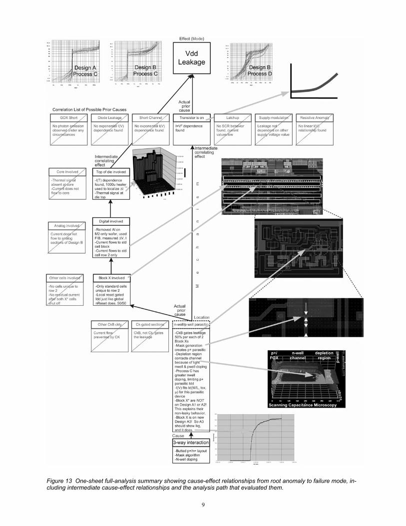
Figure 13 One-sheet full-analysis summary showing cause-effect relationships from root anomaly to failure mode, in-cluding intermediate cause-effect relationships and the analysis path that evaluated them.
9

jumping right into the middle of a new, completely imaginary analysis.
E/C/C Question. Suppose we have found, through earlier analysis, a voltage contrast anomaly (that is, our failure differs from a good part in this way.) The
anomalous contrast--our known effect--could be a re-sult of any of a number of possible prior causes, but let's select one: a conductive path between the metal trace showing the contrast and some other nearby metal trace. (The resulting short would change the trace's voltage, and therefore its contrast.) Our possi-ble prior cause, then, is an intermetal conductive path, and the E/C/C Question step would lead us to construct this question: "Does an intermetal con-ductive path exist, correlate with our observed volt-age contrast anomaly, and cause it?" Multiple ex-
amples of the use of the E/C/C Question appear in the first part of this tutorial. It will serve the reader well to review the above case study as this general de-scription of the metaprocess describes each of the metaprocess’s six steps.
Measurement. This second step uses analysis tools, observation, and logical reasoning to look for an effect of the possible prior cause--the intermetal conductive path--other than our known effect. In other words, what else would an intermetal conduc-tive path do besides create our observed contrast anomaly? When we come up with such secondary effects, we measure them at this second step. We
might, for example, measure I(V) current to adjacent lines and look for a linear relationship as an effect of an intermetal path. Such an ohmic I(V) characteristic between adjacent lines is a second, different effect of
our possible prior cause. Interpretation. We next interpret our measure-
ment results and determine what answer they give to our E/C/C Question. If we find the ohmic I(V) trace we just mentioned, we can keep our possible prior cause--intermetal conduction--as a candidate for the actual cause. We cannot yet conclude, however, that we have found the actual cause, since there are still
other possible prior causes which could explain both our observed contrast and also ohmic I(V) simultane-ously. At this point, then, we loop back to the meas-urement step (see Fig. 1) and look for yet another secondary effect of the PPC. We may look for other
effects such as Liquid Crystal phase changes, current local to the output block or to the phase change, and so on, as we continue to loop. When we actually find enough of our predicted effects, we can conclude that
their common cause, intermetal conduction, exists. If on the other hand the ohmic I(V) trace is absent,
then we immediately rule out an intermetal short, in accordance with a logic guideline called the Contra-positive Test, also discussed below.
E/C/C Answer. After interpreting our measure-ment results and finding enough evidence for our prior cause, we formulate an answer that corresponds exactly in form to the question we posed.
If and when results support it, we a) conclude that the linear I(V) exists, b) demonstrate that the I(V) trace correlates with the node’s leakage anomaly, and c) show by appropriate physical laws that any ob-served I(V) causes the leakage. We may find that our possible prior cause doesn’t exist, or we may find that it exists but that it doesn't correlate with our known anomaly, or we may find existence and correlation but not find that our PPC causes the known anomaly. Or we may find all three, existence, correlation and causation. In this case, for our example we would an-swer, "An intermetal conductive path exists, corre-lates with our observed voltage contrast behavior, and causes it." This IM conduction now becomes our new known effect, since we have proved its exis-tence and shown where it lies in the failure's cause-effect chain.
Correlation List. Now that we have a new known effect, we next create a brainstorm list of PPC's of the intermetal short. We might include lateral or vertical dielectric cracking, intermetal particles, oxide pin-holes, electromigration-induced metal extrusions, metal overheating, and so forth. We also--and this is
Ohmic I(V)! VC anomaly
IM conduction?
VC anomaly!
IM conduction!
LC phase chg?
�V near �T?
Visible metal?
T-, I-fragility?
IM conduction!
Particle? Metal extrusion?
Ohmic I(V)? VC anomaly!
IM conduction?
IM conduction!
Particle? Metal extrusion? Dielectric crack?
LC phase chg?
Ohmic I(V)! VC anomaly
IM conduction?
VC anomaly!
VC anomaly!
IM conduction?
Ohmic I(V)? VC anomaly!
IM conduction?
10

very important--generate an exhaustive list of other secondary effects of each of these possible prior causes. For example, along with our metal extrusion item we add to the Correlation List expected secon-dary effects including local liquid crystal phase change, further local voltage changes, visible metal anomaly, fragility with temperature, fragility with high current, along with any other such effects we can think of. One thing to note is that visual evidence of an anomaly has no special place in this methodol-ogy: it falls equal in importance to any other equally-attested effect. A well-built correlation list will in-clude at least ten secondary effects of each PPC. If it proves difficult to come up with many secondary ef-fects, this indicates, among other things, the need for analysts to strengthen their understanding of the physics of device failure. Our measurement step above, however, shows how important these secon-dary effects are to a successful analysis.
Selection. In the final step of our loop we select one of the Correlation List items and use it to begin a new Decision Engine cycle. We make the selection based in part on factors such as whether our choice must be investigated destructively, whether investi-gation of the PPC or effect is easy or difficult, and how likely the item is. In our example, we might se-lect local liquid crystal phase change as our effect, since it is likely, relatively easy to measure, and non-destructive. We are free to choose more than one list item, each starting its own new Decision Engine cy-cle. This methodology enables us to increase our productivity in this way while giving us a tool to keep track of where we are in each analysis direction.
E/C/C Question (next loop iteration). At this point we prepare our next E/C/C Question about this selection: "Does local liquid crystal phase change exist, correlate with the observed intermetal conduc-tion, and cause it?" The Engine cycle begins again with this step. But what has happened during these six steps plus one? We have moved from one known anomaly, a difference in voltage contrast between a good part and our failure, to the actual prior cause for that anomaly, an instance of anomalous intermetal conduction. Our single loop has taken us down one link in the unique chain of cause-and-effect that the failure contains.
Moving from Mode to Root Anomaly. This pat-tern of steps, then, demonstrably creates an analysis flow which proceeds efficiently back down the cause-effect chain by which the root anomaly creates the failure mode. If we simply apply the Decision En-gine loop, our analysis flow unfolds, and the failure's cause-effect chain relationships are revealed link by link. From the initial failure mode (question, "Does a failure mode exist on this design and correlate with
the complaint") and its verification (answer, "the mode exists and correlates with the complaint") through intermediate questions (for example., "do hillocks exist, correlate with the observed intermetal conduction, and cause the conduction?") and their an-swers, to the root anomaly ("does incomplete CMP exist in the region of the conduction, correlate with the observed conduction, and cause it?"), this metaprocess creates the analysis flow which leads the analyst from the mode, or the first detected effect of the failure cause, back through intermediate cause-ef-fect relationships to the root anomaly. In this way the metaprocess reveals the entire cause-effect chain from root anomaly to failure mode.
Analysis Flow Characteristics. Rather than de-livering a prepackaged analysis flow which may or may not apply well to the failure at hand, this metaprocess produces the analysis flow one step at a time based on actual failure characteristics. This makes the unfolding analysis flow very responsive to the most current information about the failure. The metaprocess also directs the analyst to explore appli-cable cause-effect relationships at each point, and points to needed measurement equipment and tech-niques, whether available to the analyst or not.
These characteristics provide two benefits. First, they prioritize the analyst's focus correctly, placing greater importance on an understanding of good and failing device behavior than on technique or tool op-eration expertise. Second, they encourage the devel-opment of an analytical lab infrastructure which serves the objective of finding causes of failure, rather than the other way around. Many labs unwit-tingly make the toolset primary. The analysis process then becomes in large part a way of "grading" failures to determine whether or not they will reveal their se-crets to a lab's existing analysis tool and technique set. Failures which do not yield to existing analysis capability often merely land in the "Cause unknown" bin rather than driving the lab's capability forward until their causes are found. The metaprocess de-scribed here makes the need for missing techniques both evident and quantifiable, enabling labs to im-prove their equipment set with confidence in the value of the techniques developed or purchased. (The metaprocess benefited the VDD leakage analysis by prompting the development of the topside airflow heater whose results provided the first localization of the leakage.)
Second, the flow's characteristics make the formal
VC anomaly!
IM conduction!
LC phase chg?
Design failure!
VC anomaly!
IM conduction!
Intertrace Cu!
Incomplete CMP!
11

use of inferential logic easier, so as to help avoid analysis pitfalls and improve success. The flow does so by breaking the analysis process down into seg-ments small enough that their relationship to formal logic principles becomes clear. The following sec-tion explains this for three of the most important logic concepts, namely logical inference, proof by in-duction and disproof by contrapositive testing.
Applying Formal Logic. Fig. 14 shows a seg-ment of the full six-step loop. This segment relates to how we prove and disprove possible correlations in the course of a failure analysis. For example, if we have a functional failure mode which only occurs at positive supply voltages above 2.5V, we must look for possible prior causes which imply that specific voltage dependence. These may not be easy to iden-tify. The apparent nonlinear relationship with supply voltage may suggest, however, that our failure mechanism involves active devices, and therefore may correlate with photon emission.
To investigate this possible correlation we identify implied characteristics of a common cause for the failure and the photon emission, then look for those characteristics. Simple but important logical impli-cations--if-then statements--used here begin with the clause:
"If a common cause creates the functional failure mode and photon emission, then..."
and end with clauses such as, "any observed photon emission will show an intensity
change at 2.5V"; "temperature-dependent shifts in the failure onset will correlate with observed photon intensity change"; "emission pattern will correlate with the failing vector(s)"; "good devices will not show the observed cor-relations"
and so on. Each of these implications describes a cause-effect relationship; each possible effect pro-vides something to measure.
After each measurement, an interpretation of the results indicates whether the predicted effect exists. As the list of observed effects grows, with no unsuc-cessful tests, the strength of the correlation grows with it, until the analyst can conclude that the com-mon cause exists. After a sufficient number of meas-urements, each verifying a predicted effect, we con-sider the cause proved. This process is called proof by induction. (In actual analyses, we would be very specific about exactly what common cause--gate ox-ide leakage on the input of an and-or-invert block, threshhold voltage shifts in the region of a failing
register, or poor transmission-gate design electrically close to the VDD node--we wish to demonstrate.) In-ductive proof--enough successful tests with no fail-ures--represents a powerful tool for the analyst, in spite of its subjectivity.
Should we find on the other hand that a predicted effect of our possible prior cause is clearly and de-finitively absent, we conclude that the cause is ab-sent. This needs to happen in principle only once, not repeatedly as with inductive proof. The logical prin-ciple by which we disprove such a prior cause is the contrapositive test. This test's principle states that if any cause positively implies a given effect, the real absence of that effect immediately disproves the ex-istence of the cause.
To reiterate, while it typically takes multiple it-erations of measurement and interpretation to prove a correlation and its prior cause, in principle it takes the absence of only one predicted and sure effect to dis-prove a correlation or possible prior cause.
But our use of logic tools runs throughout the en-gine. On the other side of the decision engine loop are the Correlation List and Selection steps (Fig. 15.) Where the Measurement and Interpretation steps prove or disprove whether our possible prior cause is real, the Correlation List and Selection steps identify those PPCs in order to prove or disprove them. Logi-cal principles applied at this step include, among oth-ers, logical implication, axioms of independent and dependent causes, and causation checking (identify-ing possible prior causes).
Avoiding False Paths. Logical implication, logi-cal correlation or equivalence, inductive proof, and contrapositive testing represent four of at least twelve logical principles applicable at one or more steps in the decision engine loop. Space limitations prevent a full description in this tutorial, but others govern the logic of interactions, identifying failure characteris-tics by looking for patterns, handling multiple possi-ble causes of a given effect, and justifying destructive steps. Each of these logical principles helps to iden-tify false analysis paths and avoid all but brief trips down these paths. In the process, analyses succeed more often.
For example, inductive proof directs the analyst to test repeatedly, not just once, for a possible prior cause. Many effects such as photon emission and lo-cal temperature excursions have multiple possible prior causes, of course. These must be distinguished from one another during analysis by looking for their
Figure 14 Metaprocess steps related to proving or disprov-ing possible prior causes
Measurement
Interpretation
Figure 15 Metaprocess steps related to identification of PPCs
Correlation List
Selection
12

other effects, as we described above in our descrip-tion of the Interpretation step. To make a mistake in connection with this process means an unknowing
trip down a false path. Inductive proof leads the ana-lyst to look for these false paths by finding the one prior cause whose effects all appear. In the process, the other possible (but not actual) prior causes are re-jected. For example, suppose a particular signal never makes it from one block's output to the next in-put. A clear voltage contrast change on either side of the lone contact on the failing metal line (Fig. 16) leads immediately to the initial suspicion that the contact is open or high resistance. If inductive proof is not used, the suspicion may easily become a con-clusion without further testing, which is a logically-incorrect, and risk-laden, approach. Alternatively, use of inductive proof would lead to more careful scrutiny of the downstream voltage contrast to look for harder-to-find evidence of the output signal, me-chanical microprobing to test for DC current flow across the contact, and even photon emission tests to examine the behavior of the input stage to which the trace connects. If any evidence of low-frequency, low-amplitude post-contact signal exists, or photon emission in the input stage correlates with the failing
condition, or especially if current flows normally through the contact, the analyst is immediately led away from the open contact prior cause, which is clearly in those cases a false path. A low-value short at the downstream input stage, creating a resistor di-vider with the contact, as illustrated in Fig. 17, may conceivably turn out to be more likely based on in-ductive proof's additional results.
But what might have happened if we had followed events in the pursuit of the incorrect open contact prior cause? A natural next step to evaluate an open contact would be a focused-ion-beam cross-section, clearly a destructive step. Other possible steps would produce a similar result. In fact, whatever the se-quence of analysis operations chosen, the path even-tually will include a destructive step. Therefore pur-suit of the false path would sooner or later result in a
destructive step performed prematurely and at the wrong location. This illustrates the point that de-structive steps are generally not the cause, in and of themselves, of unsuccessful analyses. Some analy-ses, in fact, are composed almost entirely of destruc-tive steps, with extremely successful results due in large part to proper and logical methodology12. Analyses fail rather because a false path is mistaken for the true path, and premature or misplaced de-structive steps remove essential evidence for the ac-tual cause-effect chain. The root anomaly then re-mains undiscovered in spite of all further analytical efforts. Good use of inferential logic within the metaprocess thus avoids improper destructive steps and increases the analysis success rate.
Analysis Speed. Execution speed may be the first concern that an analyst has with a scientific-method-based approach. This methodology addresses that concern first by efficiency. Unrecognized false paths waste more analysis time than any other time sink, not to mention the disastrous results if the analyst performs a destructive step. The remedy, testing for multiple effects of a PPC, costs far less in time than an unrecognized false path. Secondly, the method provides a level of organization that permits multiple decision engine cycles to operate in parallel without confusion, as described above. This means that the analyst can investigate several PPC’s at a time and still keep track of the analysis easily. Finally, meth-odological insights into cause-effect versus effect-ef-fect correlations and other characteristics of the main cause-effect chain enable the analyst to choose the fastest among several possible analytical routes to the root anomaly.
Uniform Analysis Representation. While pro-viding the above benefits to analysis execution, speed and success, the metaprocess described here also generates a uniform, informative and compact way to represent an entire analysis flow. When each loop's Answer and Correlation List contents are written down, the analysis path revealing the main cause-ef-fect chain, and also each investigated but disproved prior cause, appear in graphical form. A generic ex-ample of such a summary appears in Fig. 18. It may be profitably compared to the analysis summary of Fig. 13, which represents a specific instance of such a summary.
This representation lays a foundation for uniform presentation of analyses from case to case, analyst to analyst, and, for that matter, company to company. This in turn opens opportunities for better communi-cation of analysis results and methods, for training of analysts that goes beyond informal or trainer-depend-ent approaches, and for database logging of analysis results to capture the essential aspects of any analy-sis.
Conclusion. Failure analysts who repeatedly find correct causes for difficult failures come to be known as clever analysts. While such reputations may be well deserved, cleverness of this sort can and should be formalized and taught to those not yet possessing
Figure 17 Alternative PPC for observed contact VC contrast change
Figure 16 Voltage con-trast change at contact
13

such a reputation. A well-constructed, careful analy-sis methodology provides a teachable formulation for the 'cleverness factor' (which consists chiefly, in this author's opinion, of discovering, understanding the nature of, and making use of the large network of cause-effect relationships which can lead to the fail-ure's cause). It also provides a foundation for rigor-ous use of all available equipment during analysis. This tutorial has described a formal failure analysis methodology or Decision Engine which provides a speed-sensitive scientific approach for use in typical electronic-device manufacturing technologies. The approach is a metaprocess, a generic process which itself produces a specific process flow adapted to a specific failure analysis. It benefits the analyst by providing an effective custom analysis flow, keeping the analysis organized in the mind, making the ap-proach as rigorous as required for the problem's diffi-culty, providing tools to optimize speed and analysis depth, and enabling a clear and standardized descrip-tion of the analysis flow and outcomes.
References
1. Wagner, L., Failure Analysis of Integrated Cir-cuits: Tools and Techniques, pp. 1-11. 1999: Kluwer Academic Publishers, Boston, MA.
2. Dicken, H., "A Philosophy of, and a Basic Ap-
proach to Failure Analysis," Electronic Failure Analysis Seminar Reference, pp. 13-25. 1998: ASM International, Materials Park, OH.
3. Pabbisetty, S., "Failure Analysis Overview,"Electronic Failure Analysis Seminar Reference, pp. 3-11. 1998: ASM International, Materials Park, OH.
4. Ferrier, S. "A Standardized Scientific MethodApproach for Failure Analysis Application," 2002 Proceedings of the International Symposium for Testing and Failure Analysis, pp. 341-347.
5. Ferrier, Steve, "Trying to See in the Dark,"Electronic Device Failure Analysis News, May 2003, p. 25.
6. Ferrier, Steve, Martin, Kevin, and Schulte,Donald, Ph. D., Contributions of a Failure Analy-sis Metaprocess to Breakthrough Failure Analysis Results, 2003 Proceedings of the International Symposium for Testing and Failure Analysis, pp. 167-176
7. Gray, Paul R. and Robert G. Meyer, Analysisand Design of Analog Integrated Circuits, p. 64, eqn 1.175, John Wiley & Sons, New York, New York (1993).
8. Gray, Paul R. and Robert G. Meyer, Analysisand Design of Analog Integrated Circuits, p. 64,eqn 1.174, John Wiley & Sons, New York, New York (1993). Note that the temperature de-
Figure 18 Generic diagram of analysis flow showing path to each actual prior cause through observed secondary ef-fects, and elimination of incorrect possible prior causes by demonstrated absence of secondary effects. Note that each actual prior cause is itself an effect of an earlier cause in the chain. The prior cause which has no earlier cause in the failing integrated circuit is the root anomaly.
Actual prior cause!
Actual prior cause!
Secondary Effect!
Failure Mode!
Secondary Effect!
Secondary Effect!
Possible prior cause
Secondary Effect!
Secondary Effect!
Secondary Effect!
Secondary Effect!
No Secondary Effect
Actual prior cause!
Root anomaly!
No Secondary Effect
Secondary Effect!
Secondary Effect!
Possible prior cause
No Secondary Effect No Secondary Effect
No Secondary Effect No Secondary Effect
No Secondary Effect
No Secondary Effect
Possible prior cause
Secondary Effect!
Secondary Effect!
Secondary Effect!
Possible prior cause
No Secondary Effect
14


![ASM/ATFCM Procedure 3 Preliminary Safety Case · · 2014-08-144.7 Safety Process Validation and Verification ... and the Safety Case Development Manual [8] ... The ASM/ATFCM Procedure](https://static.fdocuments.net/doc/165x107/5aed86b27f8b9a45568fc890/asmatfcm-procedure-3-preliminary-safety-safety-process-validation-and-verification.jpg)

