The Effect Of Carbon Nanotube/organic Semiconductor ...
46
University of Central Florida University of Central Florida STARS STARS Electronic Theses and Dissertations, 2004-2019 2012 The Effect Of Carbon Nanotube/organic Semiconductor The Effect Of Carbon Nanotube/organic Semiconductor Interfacial Area On The Performance Of Organic Transistors Interfacial Area On The Performance Of Organic Transistors Narae Kang University of Central Florida Part of the Physics Commons Find similar works at: https://stars.library.ucf.edu/etd University of Central Florida Libraries http://library.ucf.edu This Masters Thesis (Open Access) is brought to you for free and open access by STARS. It has been accepted for inclusion in Electronic Theses and Dissertations, 2004-2019 by an authorized administrator of STARS. For more information, please contact [email protected]. STARS Citation STARS Citation Kang, Narae, "The Effect Of Carbon Nanotube/organic Semiconductor Interfacial Area On The Performance Of Organic Transistors" (2012). Electronic Theses and Dissertations, 2004-2019. 2497. https://stars.library.ucf.edu/etd/2497
Transcript of The Effect Of Carbon Nanotube/organic Semiconductor ...

University of Central Florida University of Central Florida
STARS STARS
Electronic Theses and Dissertations, 2004-2019
2012
The Effect Of Carbon Nanotube/organic Semiconductor The Effect Of Carbon Nanotube/organic Semiconductor
Interfacial Area On The Performance Of Organic Transistors Interfacial Area On The Performance Of Organic Transistors
Narae Kang University of Central Florida
Part of the Physics Commons
Find similar works at: https://stars.library.ucf.edu/etd
University of Central Florida Libraries http://library.ucf.edu
This Masters Thesis (Open Access) is brought to you for free and open access by STARS. It has been accepted for
inclusion in Electronic Theses and Dissertations, 2004-2019 by an authorized administrator of STARS. For more
information, please contact [email protected].
STARS Citation STARS Citation Kang, Narae, "The Effect Of Carbon Nanotube/organic Semiconductor Interfacial Area On The Performance Of Organic Transistors" (2012). Electronic Theses and Dissertations, 2004-2019. 2497. https://stars.library.ucf.edu/etd/2497

THE EFFECT OF CARBON NANOTUBE/ORGANIC SEMICONDUCTOR
INTERFACIAL AREA ON THE PERFORMANCE OF ORGANIC
TRANSISTORS
by
NARAE KANG
B.S Hanyang University, 2009
A dissertation submitted in partial fulfillment of the requirements
for the degree of Master of Science
in the Department of Physics
in the College of Science
at the University of Central Florida
Orlando, Florida
Fall Term
2012
Major Professor: Saiful I. Khondaker

ii
© 2012 Narae Kang

iii
To my parents and my brother

iv
ABSTRACT
Organic field-effect transistors (OFETs) have attracted tremendous attention due to their
flexibility, transparency, easy processiblity and low cost of fabrication. High-performance
OFETs are required for their potential applications in the organic electronic devices such as
flexible display, integrated circuit, and radiofrequency identification tags. One of the major
limiting factors in fabricating high-performance OFET is the large interfacial barrier between
metal electrodes and OSC which results in low charge injection from the metal electrodes to
OSC. In order to overcome the challenge of low charge injection, carbon nanotubes (CNTs) have
been suggested as a promising electrode material for organic electronic devices.
In this dissertation, we study the effect of carbon nanotube (CNT) density in CNT
electrodes on the performance of organic field effect transistor (OFETs). The devices were
fabricated by thermal evaporation of pentacene on the Pd/single walled CNT (SWCNT)
electrodes where SWCNTs of different density (0-30/um) were aligned on Pd using
dielectrophoresis (DEP) and cut via oxygen plasma etching to keep the length of nanotube short
compared to the channel length. From the electronic transport measurements of 40 devices, we
show that the average saturation mobility of the devices increased from 0.02 for zero SWCNT to
0.06, 0.13 and 0.19 cm2/Vs for low (1-5 /µm), medium (10-15 /µm) and high (25-30 /µm)
SWCNT density in the electrodes, respectively. The increase is three, six and nine times for low,
medium and high density SWCNTs in the electrode compared to the devices that did not contain
any SWCNT. In addition, the current on-off ratio and on-current of the devices are increased up

v
to 40 times and 20 times with increasing SWCNT density in the electrodes. Our study shows that
although a few nanotubes in the electrode can improve the OFET device performance, significant
improvement can be achieved by maximizing SWCNT/OSC interfacial area. The improved
OFET performance can be explained due to a reduced barrier height of SWCNT/pentacene
interface compared to metal/pentacene interface which provides more efficient charge injection
pathways with increased SWCNT/pentacene interfacial area.

vi
ACKNOWLEDGMENTS
I would like to acknowledge and give my great appreciation for his guidance and support
of my thesis advisor, Dr. Saiful I. Khondaker who has mentored me throughout my research
work over the entire time during the Master degree of Science at University of Central Florida
(UCF). Dr. Khondaker has provided a great opportunity to experience real research at
Nanoscience Technolocy Center (NSTC) at UCF and guided me throughout my research and
beyond. I also would like to thank the committee members, Dr. Lei Zhai, and Dr. Michael N.
Leuenberger for spending their valuable time to read my thesis
Secondly, I strongly would like to acknowledge Biddut Sarker and Daeha Joung for their
help operating the equipment such as e-beam lithography (EBL), e-beam/thermal evaporation,
scanning electron microscopy (SEM), atomic forced microscopy (AFM) to fabricate and
characterize the nano-scaled devices. I wish them the best of luck continuing their research and
beyond for their future career. I would also like to thank all the members in my group, Feras
Alzubi, Muhammad Rakibul Islam, and Udai Bhanu. I also would like to thank the members of
staffs and faculties at Nanoscience Technology Center (NSTC) and department of physics in
University of Central Florida (UCF).
Last of all, my special thanks have to to my family for their endless love and support.

vii
TABLE OF CONTENTS
LIST OF FIGURES ..................................................................................................................... viii
LIST OF TABLES .......................................................................................................................... x
LIST OF ABBREVIATIONS ........................................................................................................ xi
CHAPTER 1 : INTRODUCTION .................................................................................................. 1
1.1 Motivation ............................................................................................................................. 1
1.2 Organization of thesis ............................................................................................................ 5
CHAPTER 2 : BACKGROUND .................................................................................................... 6
2.1 Organic field-effect transistors (OFETs) ............................................................................... 6
2.2 Interfacial barrier at metal electrode/OSC interface.............................................................. 7
2.3 Enhanced charge injection at CNT electrode/OSC interface ................................................ 9
CHAPTER 3 : DEVICE FABRICATION .................................................................................... 12
3.1 Fabrication of electrodes ..................................................................................................... 12
3.2 Assembly of CNT using dielectrophoresis .......................................................................... 13
3.3 Fabrication of making different density CNTs in the electrodes ........................................ 14
3.4 Fabrication of OFETs using CNT electrodes ...................................................................... 18
CHAPTER 4 : ELECTRON TRANSPORT MEASUREMENT.................................................. 20
4.1 Experimental Set-up ............................................................................................................ 20
4.2 Output/Transfer characteristics of OFETs .......................................................................... 21
4.3 Device statistics ................................................................................................................... 25
CHAPTER 5 : CONCLUSION .................................................................................................... 31
5.1 Summary ............................................................................................................................. 31
5.2 Future work suggestions ...................................................................................................... 32
REFERENCES ............................................................................................................................. 33

viii
LIST OF FIGURES
Figure 1 (a) A conceptual view of future organic flexible display which can be rolled into a pen-
like device when not in use. Images courtesy of Universal Display Corp. (b) A full color, 13-inch
OLED display with only 2mm thick. (c) A conceptual view of integrated circuits on flexible, and
transparent plastic substrate. Photograph courtesy of T. Jackson, Penn state Univ. [ref. 2] .......... 1 Figure 2 Schematic of bottom-gated organic field-effect transistors (OFETs) showing the factors
that limits the performance of OFETs using the metal (Pd) electrodes.[ref. 25] ............................ 2
Figure 3 Different studies of OFETs using CNT electrodes show improved charge injection
properties and different densities of CNT in the electrodes. (a) [ref. 11], (b) [ref. 12], (c) [ref. 26],
and (d) [ref. 13] ............................................................................................................................... 3
Figure 4. (a) The basic structure of bottom-gated OFETs. It has 5 components: source, drain
electrode, insulating dielectric layer, gate electrode, and organic semiconductor. Channel length
(L) and channel width (W) was described in the schematic diagram. The working principle of
OFETs and current-voltage characteristics are illustrated in (b)-(d). (b) linear, (c) the beginning
of saturation at pinch-off, and (d) saturation regime. [ref. 27] ....................................................... 6 Figure 5. The schematic diagram of energy level difference between metal electrode and organic
semiconductor (a) without and (b) with an interfacial dipole barrier. [ref. 8] ................................ 8 Figure 6. The different types of dipole barrier formation at metal electrode/organic
semiconductor interface. [ref. 28] ................................................................................................... 9
Figure 7. The schematic theoretical diagram of CNT structure. The properties of CNTs can be
decided depending on its chirality. (a) armchair, (b) zigzag, and (c) chiral. The actual tubules
shown in the figure correspond to (n,m) values of : (a) (5,5), (b) (9,0), and (c) (10, 5). [ref. 29] 10 Figure 8. Schematic diagram of electrode pattern fabrication on the Si substrate. First, PMMA is
spincoated on the Si substrate. Then, using EBL the pattern of electrode is defined. The desired
metal is evaporated. Lift-off is done using action followed by IPA, DI water washing and drying
with N2 gun. .................................................................................................................................. 12 Figure 9. The schematic diagram of DEP assembly of CNTs. (a) The CNT solution is dropped
between source and drain electrode. (b) The simulation pictures showing electric field formation
when AC voltage is applied between source and drain electrode. (c) After applying AC voltage,
CNTs are aligned along E-field between source and drain electrode. [ref. 23] ............................ 13 Figure 10. Electrical characterizations of SWCNT aligned arrays before cutting. (a) Current (Id)
–voltage (Vd) and (b) current (Id) – gate voltage (Vg) characteristics at fixed Vds = 0.5V. .......... 14
Figure 11. Schematic diagram of SWNT electrode fabrication with different density of SWNTs
in the electrode. (i) Assembly of the aligned array SWCNTs by DEP assembly between Pd
electrodes. Linear density of the SWCNT arrays was controlled by tuning the SWCNT solution
concentration (iii) Opened a window on the SWCNTs array via electron beam lithography and
(iv) etch the SWCNTs by oxygen plasma..................................................................................... 16 Figure 12. (a) SEM images of the edge of the electrodes with high, medium, low density
SWCNTs and Pd electrode. (b) Current-voltage characteristics of the electrodes with high,

ix
medium and low density SWCNTs before cutting. Inset : AFM images of pentacene film. The
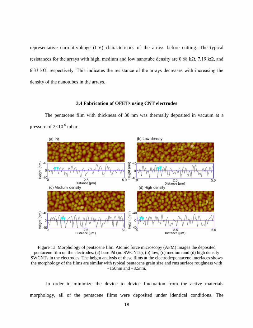
scale bar indicates 500nm for each picture. .................................................................................. 17 Figure 13. Morphology of pentacene film. Atomic force microscopy (AFM) images the
deposited pentacene film on the electrodes. (a) bare Pd (no SWCNTs), (b) low, (c) medium and
(d) high density SWCNTs in the electrodes. The height analysis of these films at the
electrode/pentacene interfaces shows the morphology of the films are similar with typical
pentacene grain size and rms surface roughness with ~150nm and ~3.5nm. ............................... 18 Figure 14. Experimental set-ups for electrical measurements of OFET devices. (a) The devices
are measured using Hewlett Packed (HP) 4145B semiconductor parametric analyzer. This is
connected to a probe station inside glove box system, which is filled with N2 gas flow as seen in
(b). ................................................................................................................................................. 20
Figure 15. Output characteristics (Id-Vdcurve) of pentacene transistors at Vg = 0, -5, -10, -15 and
-20V (bottom to top) for (a) zero, (b) low density, (c) medium density, and (d) high density
SWCNTs in the electrodes. ........................................................................................................... 21 Figure 16. Transfer characteristics (Id-Vg) of pentacene transistors at Vd = -50 V (left axis) and
(Id)1/2
(right axis) of the devices with (a) zero, (b) low density, (c) medium density, and (d) high
density SWCNTs in the electrodes. .............................................................................................. 23
Figure 17. Device performance as a function of SWCNT density in the electrodes. (a) Linear and
saturation mobility, (b) on/off ratio, and (c) on-current. ............................................................... 26
Figure 18. Schematic of diagram for (a) interfacial area and (b) the energy level diagram with (i)
bare Pd, (ii) low, and (iii) high density SWCNT in the electrodes. (a) The arrows indicate the
charge injection from the SWCNTs (red arrow) and Pd (blue arrow). (b) The schematic diagram
shows the energy level digram showing the Fermi Level (EF), HOMO and LUMO, the vacuum
level (EVAC), and the interfacial dipole (Δ) for each density electrodes. ...................................... 28

x
LIST OF TABLES
Table 1. Summary of all measured devices. The saturation mobility (μsat), linear mobility (μlin),
current on-off ratio (Ion/Ioff) and on-current (Ion) for the devices with zero, low, medium, high
density. .......................................................................................................................................... 24

xi
LIST OF ABBREVIATIONS
a-Si:H – armorphous silicon hydrogenated
CNT – carbon nanotube
DEP – dielectrophoresis
DI water – di-ionized water
EBL – electron beam lithogrphy
HOMO – highest occupied molecular orbital
IPA - isopropyl alcohol
LUMO – lowest occupied molecular orbital
N2 - nitrogen
OFET – organic field-effect transistor
OSC – organic semiconductor
P3HT – poly (3-hexylthiophene)
PMMA - Polymethylmethacrylate (Acrylic)
RFID – radio-frequency identification
SEM – scanning emission microscopy
Si – silicon
SiO2 – silicon di-oxide
SWCNT – single-walled carbon nanotube

1
CHAPTER 1 : INTRODUCTION
1.1 Motivation
Organic field-effect transistors (OFETs) have attracted a great deal of research interests
in the field of both academy and industry owing to their flexibility, transparency, low-cost and
large-area.1-4
Figure 1 (a) A conceptual view of future organic flexible display which can be rolled into a pen-like
device when not in use. Images courtesy of Universal Display Corp. (b) A full color, 13-inch OLED
display with only 2mm thick. (c) A conceptual view of integrated circuits on flexible, and transparent
plastic substrate. Photograph courtesy of T. Jackson, Penn state Univ. [ref. 2]
OFETs can be fabricated on glass or inexpensive flexible plastic substrates with lower
temperature and considerably lower cost compared to amorphous silicon hydrogenated (a-Si:H)
devices. These advantages are able to have substantial impacts on developing next generation

2
organic electronics such as flexible display, flexible solar cell, or radio-frequency identification
(RFID) tags as shown in Figure 1.
The organic semiconducting materials have been used as active channel materials for
OFETs including sublimed and solution-processed semiconductors. The most widely used
organic materials for semiconducting layer of OFETs are pentacene and poly (3-hexylthiophene)
(P3HT). Boundless choices of active materials and potentials can open up the further possibilities
for practical applications of OFETs.
Figure 2 Schematic of bottom-gated organic field-effect transistors (OFETs) showing the factors that
limits the performance of OFETs using the metal (Pd) electrodes.[ref. 25]
As the charge-injecting electrode for OFETs, conventional noble metals such as Au, Ti,
Pt, and Pd have been used due to their chemical stability and work function, which can match the
highest occupied molecular orbital (HOMO) of p-type organic semiconductors. However, the use
of metal electrodes can form several interfacial barriers at metal electrode/organic semiconductor
(OSC) such as the discontinuity in morphology, dipole barriers, and Schottky barriers, which

3
cause low charge injection at electrode/OSC interface and thus reduce the performance of
OFETs.5-9
Figure 2 shows two main factors that limits the performance of OFETs. One is low
charge injection at metal electrodes and OSC interface. The other is large grain-boundary
resistance by trapping charge carriers in grain boundaries from organic semiconductor
molecules. In order to overcome these limitations, carbon nanotubes (CNTs) have been
suggested as a promising electrode material for organic electronic devices.10-15
Figure 3 Different studies of OFETs using CNT electrodes show improved charge injection properties and
different densities of CNT in the electrodes. (a) [ref. 11], (b) [ref. 12], (c) [ref. 26], and (d) [ref. 13]
Recently, several research groups have reported the device performance of OFETs using
CNT electrodes as seen in Figure 1.3.10-18
In these studies, CNT electrodes were fabricated with
various techniques using either individual CNT,10-11
random network CNTs,15-17
CNT/polymer
composite,12
or aligned array CNTs.13,14,18
The density of CNT in the electrodes is also various
for each studies from 1 to 30 per µm. These studies also suggested that the device performance
of OFETs using CNT electrode is enhanced compared to that of OFETs using metal electrodes.

4
However, one important question is still unanswered: whether the density of CNT in the
electrode has any role in the performance of the fabricated OFETs and how much improvement
can be possible using CNT electrode? The density of CNT in the electrodes can control the
interfacial area between the CNTs and OSCs. A low density CNTs forms small CNT/pentacene
interfacial area while high density CNTs creates large interfacial area with OSC. It has been
suggested from the molecular dynamics simulation and NMR spectroscopy that a π-π interaction
exists between CNT/OSC.19-21
In addition, CNT has a field emission properties due their one-
dimensional structure.22
These theoretical and experimental studies suggest that charge injection
should depend on the CNT/OSC interfacial area and that one can improve the performance of
OFETs by maximizing CNT/OSC interfacial area. However, no such investigation has been
reported yet. Such a study is of great importance for achieving the overreaching goal of the CNT
electrodes in organic electronics.
Therefore, we systematically have investigated the effect of CNT/OSC interfacial area on
the performance of the OFETs by varying the density of CNT in the electrode. The devices were
fabricated by thermal evaporation of pentacene on the Pd/single-walled carbon nanotube
(SWCNT) electrodes where SWCNTs of different density (0-30 /µm) were aligned on Pd using
dielectrophoresis (DEP) and cut via oxygen plasma etching to keep the length of nanotube short
compared to the channel length. From the electronic transport measurements of 40 devices, we
show that the average saturation mobility of the devices increased from 0.02 for zero SWCNT to
0.06, 0.13 and 0.19 cm2/Vs for low (1-5 /µm), medium (10-15 /µm) and high (25-30 /µm)
SWCNT density in the electrodes, respectively. The increase is three, six and nine times for low,
medium and high density SWCNTs in the electrode compared to the devices that did not contain

5
any SWCNT. In addition, the current on-off ratio and on-current of the devices are increased up
to 40 times and 20 times with increasing SWCNT density in the electrodes. Our study shows that
although a few nanotubes in the electrode can improve the OFET device performance, significant
improvement can be achieved by maximizing SWCNT/OSC interfacial area. The improvement
can be explained due to a reduced barrier height of SWCNT/pentacene interface compared to
metal/pentacene interface which provides more and more efficient charge injection pathways
with increased SWCNT/pentacene interfacial area.
1.2 Organization of thesis
In Chapter 2, I will discuss the basic structure and working principle of OFETs. In
addition, I will compare the device performance of OFETs using metal electrode and CNT
electrode, showing several other groups’ study related to transport properties of OFETs using
CNT electrode compared to metal electrode.
Chapter 3 will introduce the device fabrication details of making different density CNT
electrodes using dielectrophoresis (DEP) assembly. Then, the fabrication of OFETs using
different density of CNT electrodes will be more discussed in detail.
Chapter 4 will show electron transport measurement of OFETs using different density of
CNT electrodes compared to bare Pd electrode. The output/transfer characteristics of OFETs will
be discussed depending on the different density of CNT electrodes compared to bare Pd
electrode.
Finally, in Chapter 5, I will conclude the results and suggest future works.

6
CHAPTER 2 : BACKGROUND
2.1 Organic field-effect transistors (OFETs)
The schematic diagram of organic field-effect transistors (OFETs) is described in Figure
4 (a).
Figure 4. (a) The basic structure of bottom-gated OFETs. It has 5 components: source, drain electrode,
insulating dielectric layer, gate electrode, and organic semiconductor. Channel length (L) and channel
width (W) was described in the schematic diagram. The working principle of OFETs and current-voltage
characteristics are illustrated in (b)-(d). (b) linear, (c) the beginning of saturation at pinch-off, and (d)
saturation regime. [ref. 27]

7
Basically, OFETs have three terminals: source, drain and gate. Organic semiconducting
materials can be placed between source and drain electrodes. The charge carrier density can be
modulated by applying the gate voltage. The insulating dielectric layer is placed in the middle of
the structure. We use the bottom-gated configuration for OFETs. Figure 4 (b)-(d) shows the basic
operation of OFETs showing linear and saturation current-voltage characteristics. In the linear
regime, the drain current (Id) is directly proportional to gate voltage (Vg), and the field-effect
mobility in linear regime (µlin) can be extracted from Id-Vg curve at fixed bias voltage (Vd) with
the equation of µlin = (dId/dVg)(L/WCiVd). The field-effect mobility in the saturation regime (µsat)
can be extracted using the equation of µsat = (2LId,sat)(WCi(Vg-VT)2) because the square root of
the saturation current is proportional to the Vg.
2.2 Interfacial barrier at metal electrode/OSC interface
One of the major factors which limit the performance OFET is large interfacial barrier
from the interface between metal electrodes and organic semiconductor (OSC). This causes low
charge injection from the metal electrodes to OSC and finally reduces the performance of
OFETs.5-6
The interfacial barriers can be caused by several factors such as the discontinuity in
morphology, dipole barriers, and Schottky barriers.7-9

8
Figure 5. The schematic diagram of energy level difference between metal electrode and organic
semiconductor (a) without and (b) with an interfacial dipole barrier. [ref. 8]
Figure 5 shows the schematic of metal electrode and OSC interface without and with
dipole barrier, which is originated when the vacuum level of the material is shifted. The variety
of mechanisms of interfacial dipole barrier between metal electrode/OSC is shown in Figure 6
(a)-(f). Schottky barrier is originated from a difference of energy level between work function of
metal electrode and highest occupied molecular orbital (HOMO)/ Lowest occupied molecular
orbital (LUMO) level at OSC. The presence of Schottky barrier at metal electrode/OSC interface
makes non-ohmic behavior at low bias, which is meant to be large contact resistance and low
charge injection efficiency.

9
In order to overcome those challenges of low charge injection and large interfacial barrier
between metal electrode and OSC, carbon nanotubes (CNTs) have been suggested as a promising
electrode material for organic electronic devices.10-15
Figure 6. The different types of dipole barrier formation at metal electrode/organic semiconductor
interface. [ref. 28]
2.3 Enhanced charge injection at CNT electrode/OSC interface
Carbon nanotubes (CNTs), formed by rolling up graphite sheet in three-dimension
(Figure 7.), have been suggested as promising electrode materials for OFETs.

10
Figure 7. The schematic theoretical diagram of CNT structure. The properties of CNTs can be decided
depending on its chirality. (a) armchair, (b) zigzag, and (c) chiral. The actual tubules shown in the figure
correspond to (n,m) values of : (a) (5,5), (b) (9,0), and (c) (10, 5). [ref. 29]
The physical structure of CNT is decided depending on the specific angle of rolling a sp2
bonded sheet into cylindrical shape. This angle is named ‘Chiral angle’, and the electronic
properties of CNTs is provided based on types of nanotube chirality. As seen in Figure 7,
‘armchair’ nanotubes show metallic behavior, and ‘zigzag’ nanotubes show semiconducting
behavior.
Due to their transparency, flexibility, low-cost, solution-processed and easy-processing,
CNTs have been spotlighted as a material which can be integrated to future flexible display,
flexible solar cell and many other flexible/transparent electronic applications.1-4
Owing to its
unique one-dimensional structure, CNTs have a field-emission properties and high electrical
conductivity and chemical stability. Strong π-π interaction between the side walls of CNTs and

11
organic semiconductor and high work function of CNTs (~5.0eV) is the other benefits of using
CNTs as an electrode material for OFETs.10-17

12
CHAPTER 3 : DEVICE FABRICATION
3.1 Fabrication of electrodes
The devices were fabricated on heavily doped silicon (Si) substrates coated with a
thermally grown 250 nm thick silicon di-oxide (SiO2) layer. Palladium (Pd) electrodes of 5 μm x
25 μm were fabricated using standard electron beam lithography (EBL) process. The detail
fabrication steps illustrate in Figure 8.
Figure 8. Schematic diagram of electrode pattern fabrication on the Si substrate. First, PMMA is
spincoated on the Si substrate. Then, using EBL the pattern of electrode is defined. The desired metal is
evaporated. Lift-off is done using action followed by IPA, DI water washing and drying with N2 gun.

13
The single layer resist of PMMA (950K, C2, 2%, MicroChem) is spin-coated on the Si
substrate at 4000 rpm for 1min, and then placed on hot plate to bake during 15 min at 180 ˚C.
The thickness of PMMA is 100 to 150 nm. Then, the electrode patterns are defined using EBL
(Zeiss Ultra 55 SEM) exposed with an area dose of ~ 350 μC/cm2 and voltage of 28kV. As for
the developing process, the devices are immersed into MIBK:IPA (1:3) for 75 sec and IPA for 15
sec followed by N2 dry. The desired metals, such as Au, Pd, Pt, Al, Ni, Cu, Ti, Ag and other
metals, depending upon their purpose, can be deposited by thermal/e-beam evaporation. For our
device, Palladium (Pd) is deposited by e-beam evaporation. Finally, the device is place into
Acetone for 3-4 hours to remove the rest of PMMA followed by IPA, DI water washing and N2
dry.
3.2 Assembly of CNT using dielectrophoresis
Several methods to align carbon nanotubes (CNTs) have been introduced in recent years.
The direct growth via chemical vapor deposition (CVD) is one of the examples; however, very
high temperature (~ 900˚C) is required to transfer the aligned array of CNTs to substrate.
Figure 9. The schematic diagram of DEP assembly of CNTs. (a) The CNT solution is dropped between
source and drain electrode. (b) The simulation pictures showing electric field formation when AC voltage
is applied between source and drain electrode. (c) After applying AC voltage, CNTs are aligned along E-
field between source and drain electrode. [ref. 23]

14
Since solution-processed assembly is easy-processing at room temperature, the post-
growth techniques such as Langmuir-Blodgett assembly, bubble blown assembly, evaporation-
driven self-assembly, spin coating assisted alignment and contact printing have been introduced.
However, the number of aligned CNT arrays is from 1 to 10 per um. In order to align high dense
CNT arrays, dielectrophoresis (DEP) assembly has been developed. 2D, 1D, and 0D
nanomaterials can be aligned via DEP at desirable position of the devices. Figure 3.2 describes
the schematic of DEP assembly. The basic working principle of DEP is very simple, low-cost,
solution-processed and easy-processing. 24
3.3 Fabrication of making different density CNTs in the electrodes
The single-walled carbon nanotubes (SWCNTs) of different linear densities of 0-30/um
were assembled between the Pd electrodes via DEP using a high quality SWCNT aqueous
solution obtained from Brewer Science. Figure 10. shows output/transfer characteristics of this
SWCNT solution showing metallic behavior.
Figure 10. Electrical characterizations of SWCNT aligned arrays before cutting. (a) Current (Id) –voltage
(Vd) and (b) current (Id) – gate voltage (Vg) characteristics at fixed Vds = 0.5V.

15
Figure 11. illustrated the fabrication steps of making different density of SWNT
electrodes. In short, a 3 µl SWCNT solution was dropped onto Pd pattern and an AC voltage of 5
V with a frequency of 2 MHz were applied for 30 sec. Due to the DEP force, the SWCNTs are
aligned in arrays between the Pd patterns. The linear density was controlled by varying the
concentration of SWCNT solution by diluting the original nanotube solution (~ 50 μg/mL) with
deionized (DI) water. The SWCNT arrays were then cut by spin coating PMMA, defining a 4.4
μm (L) x 25 μm (W) window in the middle of the channel using standard EBL, and subsequent
oxygen plasma etching. Finally, the chips are kept into chloroform and cleaned with isopropanol
(IPA) and deionized (DI) water

16
.
Figure 11. Schematic diagram of SWNT electrode fabrication with different density of SWNTs in the
electrode. (i) Assembly of the aligned array SWCNTs by DEP assembly between Pd electrodes. Linear
density of the SWCNT arrays was controlled by tuning the SWCNT solution concentration (iii) Opened a
window on the SWCNTs array via electron beam lithography and (iv) etch the SWCNTs by oxygen
plasma.

17
Figure 12. (a) shows representative scanning electron microscopy (SEM) images of the
part of the electrodes containing an average of 30, 13 and 2 SWCNT/um as well as a bare Pd
electrode.
Figure 12. (a) SEM images of the edge of the electrodes with high, medium, low density SWCNTs and Pd
electrode. (b) Current-voltage characteristics of the electrodes with high, medium and low density
SWCNTs before cutting. Inset : AFM images of pentacene film. The scale bar indicates 500nm for each
picture.
The average linear densities of the arrays were calculated by counting the total number of
SWCNTs from the SEM images and then dividing it by the channel width. Figure 12. (b) shows
18
representative current-voltage (I-V) characteristics of the arrays before cutting. The typical
resistances for the arrays with high, medium and low nanotube density are 0.68 kΩ, 7.19 kΩ, and
6.33 kΩ, respectively. This indicates the resistance of the arrays decreases with increasing the
density of the nanotubes in the arrays.
3.4 Fabrication of OFETs using CNT electrodes
The pentacene film with thickness of 30 nm was thermally deposited in vacuum at a
pressure of 2×10⁻⁶
mbar.
Figure 13. Morphology of pentacene film. Atomic force microscopy (AFM) images the deposited
pentacene film on the electrodes. (a) bare Pd (no SWCNTs), (b) low, (c) medium and (d) high density
SWCNTs in the electrodes. The height analysis of these films at the electrode/pentacene interfaces shows
the morphology of the films are similar with typical pentacene grain size and rms surface roughness with
~150nm and ~3.5nm.
In order to minimize the device to device fluctuation from the active materials
morphology, all of the pentacene films were deposited under identical conditions. The

19
morphological investigation using atomic force microscopy (Figure 12 (b), inset) showed that all
the films have similar morphology with an average grain size of ~150 nm (Figure 13). For a fair
comparison of the device performances in terms of nanotube density in the electrodes (different
interfacial areas) and to obtain statistically meaningful results, we classified the devices into four
categories with a narrow range of SWCNT densities: high (25-30 /μm), medium (10-15 /μm),
low (1-5 /μm) and Pd (zero SWCNT) only.

20
CHAPTER 4 : ELECTRON TRANSPORT MEASUREMENT
4.1 Experimental Set-up
The electrical transport of CNT array is measured using DL instruments 1211 current
preamplifier and Ketihly-2400 source meter interfaced with LabView program. The electronic
properties and characterization of OFETs were performed using Hewlett-Packed (HP) 4145B
semiconductor parametric analyzer interfaced with LabView program. This equipment is
connected to a probe station inside an enclosed glove box system with N2 gas flow as shown in
Figure 14. For our measurements of OFETs, a total number of 40 devices were investigated with
each different density.
Figure 14. Experimental set-ups for electrical measurements of OFET devices. (a) The devices are
measured using Hewlett Packed (HP) 4145B semiconductor parametric analyzer. This is connected to a
probe station inside glove box system, which is filled with N2 gas flow as seen in (b).

21
4.2 Output/Transfer characteristics of OFETs
In order to investigate the effect of SWCNT density in the electrodes, electrical
measurement is performed. Figures 15. (a)-(d) show the drain current (Id) vs source-drain bias
voltage (Vd) curves (output characteristics) at different gate- voltages (Vg) for our best devices
with zero, low, medium and high SWCNTs in the electrodes.
Figure 15. Output characteristics (Id-Vdcurve) of pentacene transistors at Vg = 0, -5, -10, -15 and -20V
(bottom to top) for (a) zero, (b) low density, (c) medium density, and (d) high density SWCNTs in the
electrodes.

22
All the devices show a good gate modulation with linear behavior at low Vd and
saturation behavior at higher Vd, typical of p-channel OFETs. For comparison of device
characteristics, we plotted all the curves in the same scale. From here, we see that the output
current significantly increases with increasing the SWCNT density in the electrodes. The output
current (at Vd = -50V and Vg = - 20V) of the devices with zero SWCNTs is 0.15 μA, whereas it is
0.34 μA, 0.81 μA and 1.15 μA for the devices with low, medium and high density SWCNTs in
the electrodes. The output current is twice for low density and nine times for the high density
SWCNTs compared to the device without any SWCNTs. Since the morphology of all the
devices are similar, the increase of output current with increasing SWCNT density clearly show
that the interfacial area at the SWCNTs/pentacene has significant impact on the output
characteristics of the devices.

23
Figure 16. Transfer characteristics (Id-Vg) of pentacene transistors at Vd = -50 V (left axis) and (Id)1/2
(right
axis) of the devices with (a) zero, (b) low density, (c) medium density, and (d) high density SWCNTs in
the electrodes.
To further investigate the effect of the interfacial area on the device performance, we also
measured the corresponding transfer curves (Id -Vg) of the same devices at Vd = -50 V (as seen in
Figure 16. (a)-(d)) and at Vd = -10 V and calculated the field effect mobility (μ), on-off ratio
(Ion/Ioff) and on-current (Ion) of the devices. The linear mobility, µlin (at Vd = -10 V) and
saturation mobility, μsat (at Vd = -50 V) are extracted using the standard formula,18
µlin =
(L/WCiVd)(dId/dVg) and μsat = (2LId,sat)/(WCi(Vg-VT)2), respectively; where Id,sat is saturation

24
current, and Ci is the gate dielectric capacitance (13.8nF/cm2). The maximum μsat (maximum μlin)
of the devices for zero, low, medium and high densities SWCNTs in the electrodes are 0.05
(0.03), 0.10 (0.06), 0.19(0.13), 0.29 (0.19) cm2/Vs, respectively (see also Table 1).
Table 1. Summary of all measured devices. The saturation mobility (μsat), linear mobility (μlin), current
on-off ratio (Ion/Ioff) and on-current (Ion) for the devices with zero, low, medium, high density.
This demonstrates that the mobility of the devices also increases with increasing
SWCNT/pentacene interfacial area. The maximum μsat is 100%, 280%, and 480% larger for low,
medium and high density SWCNTs in the electrode compared to the devices that did not contain
any SWCNT. Similar increment in the μlin with increasing the SWCNT density is also observed.
In calculating the μ, we used L= 4.4 µm and L= 5 µm for devices with SWCNTs and no
SWCNTs respectively. However, the SEM images of Figure 12. (a) for low and medium density
SWCNTs in the electrode show that there may be an ambiguity in determining L for these
densities as the charge injection comes from both Pd and SWCNT interface. In order to minimize
this uncertainty, we kept lengths of anchored nanotubes to the Pd short (~ 300 nm). Nevertheless,
if we were chosen L= 5 μm for these two densities then the μsat would be 0.11 and 0.22 cm2/Vs,
for low and medium SWCNT densities. These values are even higher, and indicate that our
25
experimental data exceeds the error that may arise from the choice of L in low and medium
density electrodes. In addition to μ, other important parameters to evaluate the performance of
the transistors are Ion/Ioff and Ion. The transfer curves show that the on-current (Id at Vg = - 80 V)
and Ion/Ioff increase with the nanotube density in the electrodes. The maximum Ion/Ioff and Ion for
high density SWCNT electrodes devices are 1.1×10⁵ and 14.2 μA respectively, whereas they are
3.1 ×10⁴ and 12.8 μA for medium density, 1.8 ×10
4 and 10.8 μA for low density, and 9.6 ×10
3
and 3.3 μA for zero density SWCNT in the electrodes. Therefore, both the Ion/Ioff and Ion are
also increased significantly with increasing SWCNT density in the electrodes.
4.3 Device statistics
The device characteristics measured from 40 devices are summarized in Figure 4.4 where
we plot the μ, Ion/Ioff and Ion as a function of SWCNT density in the electrodes.

26
Figure 17. Device performance as a function of SWCNT density in the electrodes. (a) Linear and
saturation mobility, (b) on/off ratio, and (c) on-current.
Figure 17. (a) show that, similar to our best devices, the average μsat are increased from
0.02 for zero SWCNT to 0.06, 0.13 and 0.19 cm2/Vs (average μlin are increased from 0.01 to 0.03,

27
0.08 and 0.11 cm2/Vs) for low, medium and high SWCNT density in the electrodes, respectively.
The increase in average mobility for our OFET with high density SWCNT electrode is almost an
order magnitude higher than that of OFETs with zero SWCNT. Similar significant increase can
also be seen in the median value of the Ion/Ioff and Ion with increasing SWCNT density (Figure
17. (b), and (c)). For the devices with zero SWCNT electrodes, the median value of Ion/Ioff and
Ion are 1.5 ×10³ and 0.6 μA, respectively. These values increased to 5.5×10
4 (~40 times) and
11.82 μA (~20 times) for the devices with high SWCNT density electrodes. From this study, it is
clear that the density of SWCNT in the electrode, which control the SWCNT/pentacene
interfacial area, has significant impact on the performance of OFETs, Our study unequivocally
show that, although a small number of SWCNTs in the electrodes can enhance the devices
performance, the maximum performance were obtained using the most dense SWCNTs in the
electrode.
The remarkable improvement in the OFET device performance with increasing the
SWCNT density in the electrodes is due to increased interfacial area of SWCNT/pentacene
interfaces. The current at an interface at a fixed bias voltage and temperature (T) can be
approximated as I ∝ exp(-ɸb/KT), where ɸb is the Schottky barrier between the
metal/semiconductor interface and K is the Boltzmann constant.14
A decrease in ɸb will result in
an increase of current at the interface. It has been recently shown that the value of ɸb at
SWCNT/pentacene interface is ~ 0.16 eV, which is much lower than the ɸb at metal/pentacene
interface (~0.35 to 0.85eV).14

28
Figure 18. Schematic of diagram for (a) interfacial area and (b) the energy level diagram with (i) bare Pd,
(ii) low, and (iii) high density SWCNT in the electrodes. (a) The arrows indicate the charge injection from
the SWCNTs (red arrow) and Pd (blue arrow). (b) The schematic diagram shows the energy level digram
showing the Fermi Level (EF), HOMO and LUMO, the vacuum level (EVAC), and the interfacial dipole (Δ)
for each density electrodes.
Figure 18. shows schematic diagrams of interfacial area for bare Pd (0 SWCNT), low and
high density SWCNT electrodes. In the devices without any SWCNT, all the charge carriers are
injected from Pd and pass through only Pd/pentacene interface (Figure 18. (a) (i)). Since Pd has a
larger barrier height compared to SWCNT, charge carriers need to overcome a larger injection
barriers at the Pd/pentacene interface, which may reduce the number of injected charge carriers
in the pentacene film and led to poor device performances (Figure 18. (b) (i)). In contrast, when a
small number of SWCNTs are anchored with Pd (low density SWCNT electrode) charge carriers

29
are injected from both the SWCNT and Pd (Figure 18. (a) (ii)). In this case, the injected charge
carriers pass through a smaller barrier at SWCNT/pentacene and a larger barrier at Pd/pentacene
(Figure 18. (b) (ii)). Since the charge carriers now have limited access of injection paths through
SWCNT, the injection efficiency and device properties are improved. With increasing SWCNT
densities, the carriers have larger SWCNT/Pentacene interfacial areas for more efficient charge
injection through the lower barrier pathways and the device properties continue to improve
resulting in higher device performance (Figure 18. (a) (iii) and (b) (iii)). It is important to note
that, in our highest density electrodes there are 30 SWCNT/µm leaving an inter-nanotube
separation of 33 nm and we are unable to increase the density any further using DEP. If it will be
possible to increase the density of SWCNT in the electrodes by any other technique, it can result
in even more impressive device performance.
It is argued that although the work function of both the Pd (5.1 eV) and SWCNT (5.0 eV)
are similar and matched with highest occupied molecular orbital (HOMO) level of the pentacene
(4.9 eV), the reduction of barrier height is occurred to only SWCNT/pentacene interface due to a
small dipole barrier forming at the SWNT/pentacene interface.14
Instead, the charge transport is
limited due to the formation of interfacial dipole barrier and Schottky barrier at Pd/pentacene
interface.7-9
Figure 18. (b) shows schematic diagrams of interfacial area and energy band diagram for
the (i) Pd/pentacene, (ii) SWCNT (low density)/pentacene, and (iii) SWCNT (high
density)/pentacene interfaces. The band diagram of energy level illustrates how the Schottky
barrier (B) and dipole barrier (Δ) are changed with interfacial area at the SWCNT/pentacene
interface. In the devices without any SWCNT, all the charge carriers are injected from the Pd and

30
pass through only Pd/pentacene interface. Since Pd has a larger barrier height compared to
SWCNT (Figure 18. (b)), charge carriers need to overcome a larger injection barrier at the
Pd/pentacene interface, which may reduce the number of injected charge carriers in the
pentacene film and lead to poor device performances. In contrast, when a small number of
SWCNTs are anchored with Pd (low density SWCNT electrode) charge carriers are injected
from both the SWCNT and Pd (Figure 18. (b)). In this case, the injected charge carriers pass
through a smaller barrier at SWCNT/pentacene and a larger barrier at Pd/pentacene. Since the
charge carriers now have limited access of injection paths through SWCNT, the injection
efficiency and device properties are improved. With increasing SWCNT densities, the carriers
have larger SWCNT/Pentacene interfacial areas for more efficient charge injection through the
lower barrier pathways and the device properties continue to improve resulting in higher device
performance.

31
CHAPTER 5 : CONCLUSION
5.1 Summary
In this thesis, we show that the performance of pentacene transistors can be significantly
improved by maximizing the interfacial area at single walled carbon nanotube
(SWCNT)/pentacene. From the electronic transport measurements, we found that the average
mobility is increased three, six and nine times for low, medium and high SWCNT densities,
respectively, compared to the devices with zero SWCNT. In addition, the current on-off ratio and
on-current are also increased up to 40 times and 20 times with increasing the SWCNT density.
Our study have demonstrated that (i) even a few nanotubes in the electrode can improve
the OFET device performance, and (ii) significant improvement can be achieved by maximizing
SWCNT/OSC interfacial area. Theses improved OFET performance can be explained by reduced
barrier height from SWCNT/pentacene interface compared to metal/pentacene interface. The
interface of high density SWCNT/pentacene provides more efficient charge injection pathways
with increased SWCNT/pentacene interfacial area. We conclude that the performance of the
pentacene transistors using aligned arrays SWCNT electrodes with various interfacial areas at the
SWCNT/pentacene contact. From the electronic transport measurement, we showed that the
OFET device performance such as mobility, current on-off ratio and on-current can be
significantly improved with increasing interfacial area at the SWCNT/pentacene and best
performance can be achieved by maximizing SWCNT/OSC interfacial area. We attributed the

32
improved device performance due to a lower barrier height at the SWCNT/pentacene interface
compared to metal/pentacene interface.
This work is supported by U.S. National Science Foundation (NSF) under Grant ECCS
1102228.
5.2 Future work suggestions
Our study showed that the density of SWCNT in the electrodes effects on the
performance of devices. The conclusion of our study suggests the way to improve the organic
field-effect transistor for future organic electronics. Also, this work will give us a better
understanding of the effect of SWCNT in the electrode in terms of the device performance. More
research can be done by low temperature transport measurement study to investigate the direct
evidence of barrier height changes depending on the densities of SWCNT in the electrodes. This
research will provide us a numerical value for the actual barrier height at different density of
SWCNT and organic semiconducting thin film, which will be varied depending on the density of
SWCNT in the electrodes.
Another potential future plan could be fabricating OFETs using graphene electrode. Due
to its unique 2-dimensional hexagonal carbon atom structure, graphene has outstanding electrical,
mechanical, and chemical properties. This study can give us an idea of improving the
performance organic field-effect transistor.

33
REFERENCES
1. C. D. Dimitrakopoulos and P. R. L. Malenfant, Adv. Mater. 14, 99 (2002).
2. S. R. Forrest, Nature 428, 911 (2004).
3. A. Dodabalapur, Mater. Today 9, 24 (2006).
4. T. B. Singh and N. S. Sariciftci, Annu. Rev. Mater. Res. 36, 199 (2006).
5. D. J. Gundlach, L. Zhou, J. A. Nichols, T. N. Jackson, P. V. Necliudov, and M. S. Shur, J.
Appl. Phys. 100, 024509 (2006).
6. L. Burgi, T. J. Richards, R. H. Friend, H. Sirringhaus, J. Appl. Phys. 94, 6129 (2003).
7. S. Braun, W. R. Salaneck, and M. Fahlman, Adv. Mater. 21, 1450 (2009).
8. I. G. Hill, A. Rajagopal, A. Kahn, and Y. Hu, Appl. Phys. Lett. 73, 662 (1998).
9. N. Koch, A. Kahn, J. Ghijsen, J.-J. Pireaux, J. Schwartz, R. L. Johnson, and A. Elschner,
Appl. Phys. Lett. 82, 70 (2003).
10. P. Qi, A. Javey, M. Rolandi, Q. Wang, E. Yenilmez, and H. Dai, J. Am. Chem. Soc. 126,
11774 (2004).
11. C. M. Aguirre, C. Ternon, M. Paillet, P. Desjardins, and R. Martel, Nano Lett. 9, 1457
(2009).
12. S. L. Hellstrom, R. Z. Jin, R. M. Stoltenberg, and Z. Bao, Adv. Mater. 22, 4204 (2010).
13. B. K. Sarker and S. I. Khondaker, Appl. Phys. Lett. 100, 023301 (2012).
14. B. K. Sarker and S. I. Khondaker, ACS Nano 6, 4993 (2012).

34
15. A. Southard, V. Sangwan, J. Cheng, E. D. Williams, and M. S. Fuhrer, Org. Electron. 10,
1556 (2009).
16. C.-H. Chang, C.-H. Chien, and J.-Y. Yang, Appl. Phys. Lett. 91, 083502 (2007)
17. Q. Cao, Z.-T. Zhu, M. G. Lemaitre, M.-G. Xia, M. Shim, and J. A. Rogers, Appl. Phys.
Lett. 88, 113511 (2006).
18. B. K. Sarker, J. Liu, L. Zhai, and S. I. Khondaker, ACS Appl. Mater. Interfaces 3, 1180
(2011).
19. J. Chen, H. Liu, W. A. Weimer, M. D. Halls, D. H. Waldeck, and G. C. Walker, J. Am.
Chem. Soc. 124, 9034 (2002).
20. M. Foroutan and A. T. Nasrabadi, J. Phys. Chem. B 114, 5320 (2010).
21. F. Tournus, S. Latil, M. I. Heggie, and J. C. Charlier, Phys. Rev. B 72, 075431 (2005).
22. G. Xhou, W. Duan and B. Gu, Phys. Rev. Lett. 87, 095504 (2001)
23. S. Shekhar, P. Stokes, and S. I. Khondaker, ACS Nano 5, 1739 (2011).
24. B. K. Sarker, M. R. Islam, F. Alzubi, and S. I. Khondaker, Mater. Express 1, 80 (2011).
25. B. J. Jung, N. J. Tremblay, M-L. Yeh, and H. E. Katz. Chem. Mater. 23, 568, (2010)
26. F. Cicoira, C. M. Aquirre, and R. Martel, ACS Nano, 5, 283 (2011)
27. J. Zaumeseil and H. Sirringhaus, Chem. Rev. 107, 1296 (2007)
28. Z. Liu, M. Kobayashi, B. C. Paul, Z. Bao, and Y. Nishi, Phys. Rev. B 82, 035311 (2010)
29. M. S. Dresselhaus, G. Dresselhaus, and R. Saito, Carbon, 33, 883 (1995)