The Digital Logic LevelThe Digital Logic...
75
The Digital Logic Level The Digital Logic Level Chapter 3 1
Transcript of The Digital Logic LevelThe Digital Logic...

The Digital Logic LevelThe Digital Logic Level
Chapter 3
1

Gates and Boolean Algebra (1)
(a) A transistor inverter.(b) A NAND gate(b) A NAND gate.(c) A NOR gate.
2

Gates and Boolean Algebra (2)
The symbols and functional behavior for the five basic gates.(d) X= A . B(d) X A . B(e) X= A + B
3

Boolean Algebra
(a) Truth table for majority function of three variables (A,B,C).O/P is 0 if the majority of its I/P are 0. 1 if the majority of its I/P 1(b) A circuit for (a)(b) A circuit for (a).
4

Circuit Equivalence (1)
C t ti f ( ) O (b) d ( ) O tConstruction of (a) NOT, (b) AND, and (c) OR gates using only NAND gates or only NOR gates. 5

Circuit Equivalence (2)
Two equivalent functions (a) AB + AC, (b) A(B + C).6

Circuit Equivalence (3)
Some identities of Boolean algebra.7

Circuit Equivalence (4)
Alternative symbols for some gates:y g(a) NAND, (b) NOR, (c) AND, (d) OR
8

Circuit Equivalence (5)
(a) The truth table for the XOR function(a) The truth table for the XOR function.(b-d) Three circuits for computing it. 9

Circuit Equivalence (6)
(a) Electrical characteristics of a device.(b) Positive logic(b) Positive logic.(c) Negative logic.
10

Integrated Circuits
An SSI chip containing four gates.SS c p co ta g ou gatesSSI : Small scale integrated (1 to 10 gates)MSI : medium scale integrated (10 to 100 gates)LSI : large scale integrated (100 to 100,000 gates)VLSI: very large scale integrated >100,000 gates)11

Combinational CircuitsMultiplexers (1)
• An eight-input / d d i/• o/p depends on i/p
• n control i/p, i/p is 2n, 1o/p•Multiplexer circuit Used to•Multiplexer circuit. Used to select one of the i/p •Used as parallel-to-serial cct•Application: keyboard
12

Multiplexers (2)
(a) An MSI multiplexer.(b) Th l i l i d h j i f i(b) The same multiplexer wired to compute the majority function.
13

Decoders
n bits i/p, used to set one of the o/p 2n to 1.
Small memory consist of 8 chipsconsist of 8 chips
A 3-to-8 decodercircuitcircuit.
14

Comparators
A simple 4-bitcomparator.
o/p is 1 if A=Bo/p is 1 if A=Bo/p is 0 otherwise
15

Programmable Logic Arrays
A 12-input 6-outputA 12 input, 6 outputprogrammable logic array.The little squares representfuses that can be burned out.fuses that can be burned out.
16

Arithmetic CircuitShiftersShifters
A 1-bit left/right shifter.• 8 i/p 8 o/p control line C determine the direction of the shift• 8 i/p , 8 o/p, control line C determine the direction of the shift
0 for left , 1 for right 17

Adders (1)
(a) (b)
(a) A truth table for 1-bit addition.(b) A circuit for a half adder.
18

Adders (2)
(a) Truth table for a full adder.( )(b) Circuit for a full adder ( has carry i/p &o/p).
19

Arithmetic Logic Units ALU (1)
• A 1-bit ALU.•Perform AND, OR sum of twoOR, sum of two machine word.•The cct perform pAB, A+B, notB based on F0, F1(00 01 10 11)(00,01,10,11)
20

Arithmetic Logic Units (2)
Eight 1-bit ALU slices connected to make an 8-bit ALU. The enables and invert signals are not shown for simplicity.
21

Clocks
(a) A clock.(b) The timing diagram for the clock(b) The timing diagram for the clock.(c) Generation of an asymmetric clock.
22

Memory (1 bit )Latches (1)Latches (1)
(a) NOR latch in state 0.(b) NOR latch in state 1.(c) Truth table for NOR(c) Truth table for NOR.
23

Latches (2)
A l k d SR l t hA clocked SR latch.24

Latches (3)
A l k d D l t hA clocked D latch.25

Flip-Flops (1)
(a) A pulse generator.(b) Timing at four points in the circuit.
26

Flip-Flops (2)• FF: the state transition does not occur when the clock is 1 but during the clock transition from 0 to 1 or 1 to 0.• FF is edge triggered, whereas a latch is level triggerFF is edge triggered, whereas a latch is level trigger
A D fli flA D flip-flop.27

Flip-Flops (3)
D latches and flip-flops.
a & b latch, c& d FF
28

Flip-Flops (4)
D l D fli flDual D flip-flop.29

Flip-Flops (5)
Octal flip-flop.Octal flip flop.
30

Memory Organization (1)Organization (1)•Logic diagram for four 3-bit (4 x 3) memory.
E h i f th• Each row is one of the four 3-bit words.• 8 i/p and 3 o/p.p p•(I0,I1,I2) are data, (A0,A1) are address, three for control CS for chipcontrol, CS for chip select, RD for read-write, OE for o/p enable. th / d tthree o/p data•To select this chip, CS, RD, (A0,A1) , ( 0, 1)
31

Memory Organization (2)
(a) A noninverting buffer.(b) Effect of (a) when control is high.(c) Effect of (a) when control is low.(d) An inverting buffer.
32

Memory Chips (1)
Two ways of organizing a 4-Mbit memory chip.(a) 19 address lines needed to address 219 bytes, 8 data
in, out(b) Asserting rather than high or low . Opposite is negated(c) WE write enable , fig b 1 i/p & o/p arranged as 2048 X
2048 matrix
33
2048 matrix(d) RAS (Row address strobe), CAS (Column address
strobe)

Memory Chips (2)
T f i i 512 Mbit hiTwo ways of organizing a 512 Mbit memory chip.34

Nonvolatile& volatile Memory Chips
A comparison of various memory types.• RAM: Random Access Memory, read and write, static and dynamic,RAM: Random Access Memory, read and write, static and dynamic, static consists of FF , used for level 2 cache memory, very fast . Dynamic consists of cell each has transistor and tiny capacitor, need refresh( reloaded), small size , slow• DDR (Double Data Rate) Synchronous DRAM, produce data on the rising and falling edge (Synchronous : waits for a clock signal before responding to control inputs )• ROM (Read only memory)• ROM (Read only memory) • EEPROM is byte erasable, Flash is a block erasable and rewritable
35

CPU Chips
• The logical pinout of a generic CPU. The arrowsindicate input signals and output signals The shortindicate input signals and output signals. The shortdiagonal lines indicate that multiple pins are used. For aspecific CPU, a number will be given to tell how many.•Pins divided into three types : address data and•Pins divided into three types : address, data, andcontrol
36
CPU Chips•The control pins are grouped into: Bus control, interrupts, Bus arbitration, Coprocessor, Status, Miscellaneous., p , ,
• Bus control : Telling whether the CPU wants to read or write.
• interrupts : I/O assert a signal to the CPU and having it service the I/O device.
B bit ti R l t t ffi th b• Bus arbitration : Regulate traffic on the bus
• Coprocessor : Floating point chips
•Miscellaneous : Reset
37

Computer Buses (1)
A t t ith lti l b ( t lA computer system with multiple buses.(external or internal) 38

Computer Buses (2)
Examples of bus masters and slaves.Master: is the active one Slave : is the passive one
39

Bus Width
Growth of an Address bus over time.New: Multiplexed busNew: Multiplexed bus
40

Bus Clocking (1)
Read timing on a synchronous busRead timing on a synchronous bus.41

Bus Clocking (2)
Specification of some critical times.
42

Asynchronous Buses
O ti f h bOperation of an asynchronous bus.43

Bus Arbitration (1)( )• What happens if two or more devices want to become bus master at the same time. I/O, CPU wants to read memory
• Many CPUs have a bus arbiter built into the CPU chip, but sometimes a separate chip is needed.
• When the device physically closet to the arbiter sees the grant, it checks to see if it made a request . If so, it takes over the bus but does not propagate the grant further down the line. If it has not made a request, it propagate the grant to the next device in the line (daisy chaining)propagate the grant to the next device in the line. (daisy chaining)
• Bus arbiter may have more than one level (2, 4,8,16) . Each device is attached to certain level and take priority.
• CPU is given the lowest priority.
• Modern computer systems put the memory on a separate bus from the
44
Modern computer systems put the memory on a separate bus from the I/O devices so that they do not have to compete for accessing the bus.

Bus Arbitration (1)
(a) A centralized one-level bus arbiter using daisy chainingchaining.
(b) The same arbiter, but with two levels. 45

Bus Arbitration (2)
Decentralized bus arbitration.
46

Bus Operations (1)
A block transfer.A block read of 4 words and takes 6 cyclesA block read of 4 words and takes 6 cycles
47

Bus Operations (2)
Use of the 8259A interrupt controller.• When the CPU commands an I/O it usually expect an• When the CPU commands an I/O, it usually expect an
interrupt when the work is done• Multiple devices, assign priority to each one and use arbiter
to give priority to the most criticalg p y• CPU handles the INT, gives INTA (ACK). • 8259 issues the number of the device on the data bus, the
CPU hardware uses this number to index into a table ofpointers ( interrupt vectors ) to find the address of theprocedure to run to service the interrupt.

Examples CPU: Pentium 4
The Pentium 4 physical pin out.
49

• Human hairs range from 20 microns to 100 microns in diameter.Pentium 4
Human hairs range from 20 microns to 100 microns in diameter.
• P4 has 55 million of transistors running at speeds up to 3.2 GHz
Li idth i 09 i• Line width is .09 micron.
• It has deeper pipeline and two ALU.
• Some models of P4 have two level cache and some have 3 levels.All models have an 8-KB on chip SRAM (L1), the second levelcache holds up to 256 KB of memory in the older models and up to1 MB in the newer ones1 MB in the newer ones.
• P4 extreme edition has 2-MB level cache 3.
• Two primary external buses, synchronous. The memory bus is used to access the main SDRM, the PCI bus is used to talk to I/O devices.
50• P4 consumes between 63watts and 82 watts.

The Pentium 4’s Logical Pinout
• Logical pinout of the Pentium 4. • Names in upper case are the officialcase are the official Intel names for individual signals. N i i d•Names in mixed case
are groups of related signals or signal descriptions.• P4 is 64- bit machine
51

P4• # symbol indicates that the signal is asserted low
0• BR0 is used to request the bus. • BR1 allows the device to make a high priority request.• LOCK allows CPU to lock the bus.• Address is 36 bits , 64 GBAddress is 36 bits , 64 GB• ADS signal is asserted to tell the target (memory) that the address lines is valid• REQ indicate the type of the bus cycle (read on word or write a bl k)block)• Five error lines are used to report floating-point errors, internal errors, machine check.• Response group contains signals used by the slave to report back to p g p g y pthe master• RS contains the status code. TRDY indicates that the slave is ready to accept data from the master.• BNR is used to assert a wait state when the target addressed cannot• BNR is used to assert a wait state when the target addressed cannot respond on time. D is used to put 8 data bytes onto the bus .• DRDY is asserted to announce their presence.• DBSY is used to tell the world that the bus is currently busy.
52
• RESET is used to rest the CPU

Pipelining on the Pentium 4’s Memory Bus
Pipelining requests on the Pentium 4’s memory busPipelining requests on the Pentium 4 s memory bus.
53

The UltraSPARC III (1)
The UltraSPARC III CPU chip.• It was introduced in 2000 at 600 MHz using .18 microns ,It was introduced in 2000 at 600 MHz using .18 microns ,
29 millions of tr.• In 2002 the lines width dropped to .13 and the clock was
raised to 1.2GHsraised to 1.2GHs• Required 50 watts
54

The UltraSPARC III (2)
Th i f t f th f Ult SPARC IIIThe main features of the core of an UltraSPARC III system. 55

The 8051 (1)
Ph i l i t f th 8051Physical pinout of the 8051.56

The 8051 (2)
Logical pinout of the 8051.It has 16 address lines , it can address up to 64 KB of memory, data bus is 8 bits .32 I/O lines , each can be attached to button, switch. It has 4 KB of internal ROM A contains the 16 address line , D are 8 used for data transport, multeplexed A address RD and WR for external memory if neededRD and WR for external memory if needed.ALE (address latch enable) used when external memory present, PSEN (program store enable) 8051 wants to read from program memory, EA (external access) if high use the internal memory, TXD and RXD allow serial I/O, RST external device to reset the chipreset the chip
57
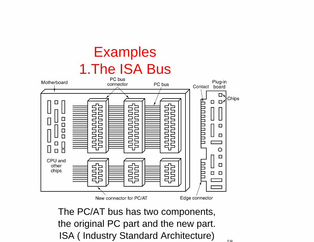
Examples1.The ISA Bus1.The ISA Bus
The PC/AT bus has two components, the original PC part and the new partthe original PC part and the new part.ISA ( Industry Standard Architecture)
58

2.The PCI Bus • PCI bus (Peripheral Component Interconnect bus).• The original PCI bus transferred 32 bits per cycle and ran at 33 MHz (30 nsec• The original PCI bus transferred 32 bits per cycle and ran at 33 MHz (30 nseccycle time) for a total bandwidth of 133 MB/sec.
• The PCI bus runs at up to 66 MHz and can handle 64-bit transfers, for a total bandwidth of 528 MB/secbandwidth of 528 MB/sec.
•AGP bus ( Accelerated Graphics Port bus ).
• The PCI bus is synchronous like all PC buses going back to the original IBM PC• The PCI bus is synchronous, like all PC buses going back to the original IBM PC
• All transactions on the PCI bus are between a master, officially called the initiator,and a slave, officially called the target
• The address and data lines are multiplexed. In this way, only 64 pins are needed on PCI cards for address plus data signals.• On a read operation, during cycle 1, the master puts the address onto the bus. Oncycle 2 the master removes the address and the bus is turned around so the slavecycle 2 the master removes the address and the bus is turned around so the slavecan use it. On cycle 3, the slave outputs the data requested.
• On write operations, the bus does not have to be turned around because themaster puts on both the address and the data
59
master puts on both the address and the data.

2.The PCI Bus (1)
Architecture of an early Pentium system. The thicker buses have more bandwidth than the thinner ones but thehave more bandwidth than the thinner ones but the
figure is not to scale. 60

The PCI Bus (2)( )
The bus structure of a modern Pentium 4.61

PCI Bus Arbitration
The PCI bus uses a centralized bus arbiter.
PCI b bit ti t li d b bit• PCI bus arbitration uses a centralized bus arbiter.• The bus arbiter is built into one of the bridge chips.• Every PCI device has two dedicated lines running from it to the arbiter.One line, REQ#, is used to request the bus. The other line, GNT#, is used
62
, Q , q , ,to receive bus grants.•To request the bus, a PCI device (including the CPU), asserts REQ# and

PCI Bus Signals(1)
M d t PCI b i lMandatory PCI bus signals.
•The Master (initiator) and Slave (target) columns tell who asserts
63
( ) ( g )the signal on a normal transaction.•PCI bus transaction begins at the falling edge of CLK

PCI Bus Signals(2)
O ti l PCI b i lOptional PCI bus signals.64

PCI Bus Transactions
Examples of 32-bit PCI bus transactions. The first three cyclesthree cycles
are used for read operation, then an idle cycle, and then
three cycles for a write operation.65

PCI Express
A t i l PCI E tA typical PCI Express system.66

PCI Express Protocol Stack
(a) The PCI Express protocol stack.(b) The format of a packet.(b) The format of a packet.
67

The Universal Serial Bus (USB)(USB)
• A USB system consists of a root hub that plugs into the main bus, This hub has sockets for cables that can connect to I/O devices.• The topology of a USB system is a tree with its root at the root hub, inside the computer.
The cable consists of four wires: two for data one for power (+5• The cable consists of four wires: two for data, one for power (+5volts), andone for ground.
•There is no traffic between two I/O devices.
• Every 1.00 ± 0.05 msec, the root hub broadcasts a new frame to keep all the devices synchronized in timekeep all the devices synchronized in time.
68

The Universal Serial Bus (USB)
The USB root hub sends out frames every 1.00 ms.SOF (Start of Frame) packet
69

The Universal Serial Bus (USB)(USB)
•USB supports four kinds of frames: control, isochronous, bulk, andinterrupt.p
•Control frames are used to configure devices, give them commands, andinquireabout their statusabout their status.
•Isochronous frames are for real-time devices such as telephones.
• Bulk frames are for large transfers to or from devices with no real-time requirements such as printers.
• interrupt frames are needed because USB does not support interrupts• interrupt frames are needed because USB does not support interrupts.
70

• A frame consists of one or more packets, possibly some in each direction. Four kinds
The Universal Serial Bus (USB)
p p yof packets exist: token, data, handshake, and special.
• Token packets are from the root to a device and are for system control. SOF, IN, andOUT packets are token packets, SOF (Start of Frame) packet is the first one in eachp p ( ) pframe and marks the beginning of the frame. IN token packet is a poll, asking the deviceto return certain data, Fields in the IN packet tell which bit pipe is being polled so thedevice knows which data to return, OUT token packet announces that data for thedevice will follow.
• DATA (used to transmit up to 64 bytes of information either way).
• handshake packets are defined: ACK (the previous data packet was correctlyp ( p p yreceived), NAK (a CRC error was detected), and STALL (please wait—I am busy rightnow).
•USB1 speed is 1.5 Mbps, USB 2 speed is 480 Mbps
•FireWire speed 400 Mbps, 800 Mbps
71

I/P CHIPS
• Chips UART (universal Asynchronous Receiver Transmitter).• PIO (Parallel Input/ output)
PIO Chips
A 8255A PIO hiAn 8255A PIO chip.72

Address Decoding (1)
L ti f th EPROM RAM d PIO i 64 KBLocation of the EPROM, RAM, and PIO in our 64 KB address space. 73

Address Decoding (2)
Full address decodingFull address decoding.EPROM: 00000XXXXXXXXXXXRAM : 10000XXXXXXXXXXXPIO : 11111111111111XX
74

Address Decoding (3)
Partial address decoding.EPROM: 1XX……..RAM : 10XXX…PIO : 11XXXXPIO : 11XXXX…..
75