The Design of a High Dynamic Range MOS Image Sensor in 110nm
93
I The Design of a High Dynamic Range CMOS Image Sensor in 110nm Technology Yang Liu (4123913) Supervisor: prof. dr. ir. Albert J.P. Theuwissen Submission to The Faculty of Electrical Engineering, Mathematics and Computer Science In Partial Fulfillment of the Requirements For the Degree of MASTER OF SCIENCE In Electrical Engineering Delft University of Technology August 2012
Transcript of The Design of a High Dynamic Range MOS Image Sensor in 110nm

I
The Design of a High Dynamic Range
CMOS Image Sensor in 110nm Technology
Yang Liu (4123913)
Supervisor: prof. dr. ir. Albert J.P. Theuwissen
Submission to
The Faculty of Electrical Engineering,
Mathematics and Computer Science
In Partial Fulfillment of the Requirements
For the Degree of
MASTER OF SCIENCE
In Electrical Engineering
Delft University of Technology
August 2012

II
COMMITTEE MEMBERS:
Prof. dr. ir. Albert J.P. Theuwissen
Prof. dr. ir. Edoardo Charbon
Dr. Guy Meynants

III
Acknowledgements
It is not easy to start a new life abroad, but with the help of a lot of kind people it
becomes easy and interesting. Here, I would like to give my sincere thanks to a lot of
people who make these two years of mine really enjoyable.
First of all, I would like to thank my supervisor, Prof. Albert Theuwissen, for giving
me an opportunity to study on such an interesting topic. His kindness helps me to go
through all difficulties I used to have. I really appreciate all his support,
encouragement and patient along my study.
Secondly, I would like to thank my daily supervisor, Dr. Xinyang Wang, for giving me
countless help both in study and living. Whenever I was confused, he could always
practically lead me to overcome the difficulties. I will cherish the memory of study
under his supervision. He is not only a scrupulous supervisor but also a great friend.
Also, I want to thank my promoter, Dr. Guy Meynants. His kindness and support
provide me the opportunity to complete my master thesis at CMOSIS Image Sensors,
Belgium. Besides, a lot of meaningful and interesting discussions with him make the
thread of my thesis clearer.
I would like to thank my mentor, Dr. Xu Wu for her kindness and patience in the past
year. She spent a lot of time on guiding my study, which makes my understanding
more profoundly. I really want to thank for her support.
I also would like to thank Cheng Ma. His help speeded up the procedure I explored to
understand the interesting and beautiful CMOS image sensor world. .
I would like to thank Gerd Beeckman, Jia Guo and other colleagues who have ever
given me help in the study. Thanks for the knowledge sharing and friendly
discussions.
In addition, I would like to thank my friends: Yingjiao Li, Yang Li, Yao Cheng, Xiaoliang
Ge, Haoyan Xue, Fengli Wang, Long Kong, Zhuowei Liu, Sijie Zeng and Jing Ling for
the happy time shared with them.
Last but definitely not the least, I want to thank my beloved families. It is their
understanding, support and encouragement that drive me forward. Undoubtedly,
the most memorable moments in my life are the time shared with them. I do
appreciate their love. I owe them too much and I will requite their love by my whole
life.
Yang Liu
Antwerp, July, 2012

IV
Abstract
This thesis presents the design of a dual-transfer-gate high dynamic range CMOS
image sensor.
Several methods that can be applied to extend the dynamic range have been
developed. However, all of these solutions have undesired problems, such as
nonlinearity response, higher dark current shot noise and discontinues signal-to-
noise ratio. In this thesis, a dual-transfer-gate pixel which can achieve 84.5dB
dynamic range is implemented in a 110nm CMOS image sensor technology. The
sensor provides 76fps speed in 12-bit digital format. The equivalent input noise is as
low as 3.1e- by introducing correlated-double-sampling (CDS) technology.
An auto-scaling ramp generator which could produce 12-bit accuracy in the working
range from 50MHz to 600MHz clock frequency is developed in the design. This high
performance ramp generator could provide various slopes for the column ADC
according to the requirement. The slope can vary from 0.112μV/s to 1.266μV/s.
Key words: High dynamic range, Ramp generator, Column ADC, Bandgap, Multiplexer

V
Table of Contents
Chapter 1 Introduction ................................................................................................... 1
1.1. Background ................................................................................................. 1
1.1.1. Basic operation principle .................................................................. 2
1.1.2. Technique scaling .............................................................................. 4
1.2. Motivation ................................................................................................... 5
1.3. Design overview .......................................................................................... 6
1.4. Thesis organization ...................................................................................... 9
1.5. Reference .................................................................................................... 9
Chapter 2 CMOS Image Sensors................................................................................... 11
2.1. Evolution of pixel structures ..................................................................... 11
2.1.1. Passive Pixel Sensor ........................................................................ 11
2.1.2. Active Pixel Sensor .......................................................................... 13
2.1.3. Back-side illumination sensor ......................................................... 15
2.1.4. Summary ......................................................................................... 16
2.2. Conventional pixel structures.................................................................... 16
2.2.1. Rolling shutter pixel ........................................................................ 17
2.2.2. Global shutter pixel ......................................................................... 19
2.3. High dynamic range pixels ......................................................................... 20
2.3.1. Logarithmic response HDR CMOS image sensors ........................... 21
2.3.2. A lateral overflow integration capacitor implemented HDR
sensor……………………………………………..………………………………………….22
2.3.3. Multiple exposure-time HDR sensor .............................................. 24
2.4. Analog readout circuitry............................................................................ 25
2.5. References ................................................................................................. 28
Chapter 3 Design of a 6T dual transfer gates high dynamic range pixel ...................... 31
3.1. Specifications of image sensor .................................................................. 31
3.1.1. Conversion gain............................................................................... 31
3.1.2. Full well capacity ............................................................................. 31
3.1.3. Signal to noise ratio ........................................................................ 32

VI
3.1.4. Dynamic range ................................................................................ 32
3.1.5. Fill factor ......................................................................................... 32
3.1.6. Resolution ....................................................................................... 33
3.1.7. Power consumption ........................................................................ 33
3.2. Noises in CMOS image sensor ................................................................... 33
3.2.1. Temporal noise................................................................................ 34
3.2.2. Fixed pattern noise ......................................................................... 36
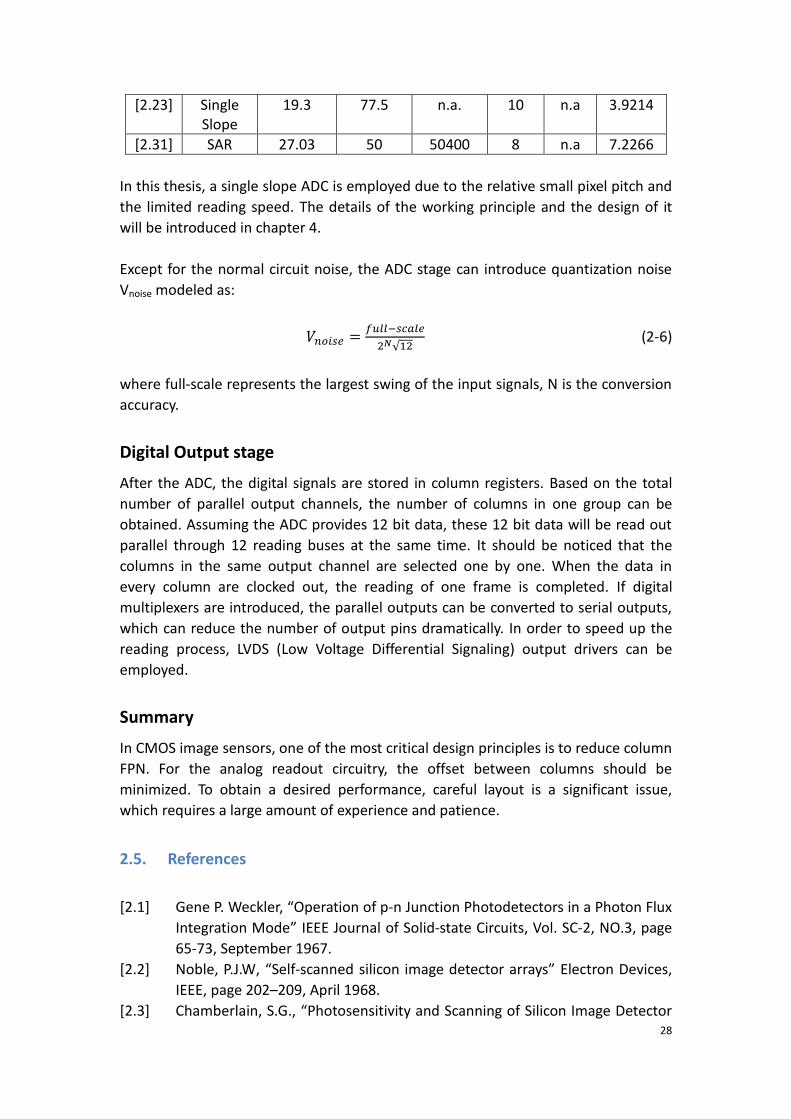
3.3. The pixel design ......................................................................................... 37
3.3.1. Principle .......................................................................................... 38
3.3.2. Layout considerations ..................................................................... 39
3.4. Parameters estimation and calculation..................................................... 43
3.5. Photon transfer curve ............................................................................... 48
3.6. Summary ................................................................................................... 50
3.7. Reference .................................................................................................. 51
Chapter 4 Design of Readout Circuitry......................................................................... 52
4.1. Overview ................................................................................................... 52
4.2. Auto-scaling ramp generator .................................................................... 53
4.2.1. Linearity .......................................................................................... 54
4.2.2. Principle .......................................................................................... 55
4.2.3. The design ....................................................................................... 56
4.2.4. Simulation results ........................................................................... 58
4.2.5. Layout ............................................................................................. 64
4.3. A/D conversion block ................................................................................ 64
4.3.1. Principle .......................................................................................... 65
4.3.2. Simulations ..................................................................................... 66
4.4. Bandgap reference .................................................................................... 67
4.4.1. Principle .......................................................................................... 67
4.4.2. Layout considerations ..................................................................... 68
4.4.3. Simulation results ........................................................................... 70
4.4.4. Summary ......................................................................................... 72

VII
4.5. Biasing circuit ............................................................................................ 73
4.5.1. 6-bit digital to analog convertor ..................................................... 73
4.5.2. Rail-to-rail buffer ............................................................................. 74
4.5.3. Layout ............................................................................................. 76
4.6. Multiplexer ................................................................................................ 77
4.6.1. Principle .......................................................................................... 77
4.6.2. Sequence generation block ............................................................ 78
4.6.3. Simulation results ........................................................................... 79
4.7. Noise calculation ....................................................................................... 81
4.8. Frame speed calculation ........................................................................... 83
4.9. Summary ................................................................................................... 84
4.10. Reference .................................................................................................. 84
Chapter 5 Conclusions and future work ...................................................................... 85
5.1. Conclusions ............................................................................................... 85
5.2. Future work ............................................................................................... 85

1
Chapter 1 Introduction
After being introduced in the mid of past century, solid state image sensors have
been widely implemented in various applications, such as security monitor, machine
vision camera, and digital still cameras etc. CCD (charge-coupled-device) and CMOS
(complementary metal oxide semiconductor) image sensors were both invented in
1960s and 1970s. In 1963, Morrison made a first successful MOS image sensor [1.1],
followed by Horton in 1964 [1.2] and Schuster from Westinghouse in 1966 [1.3]. The
other kind of solid-state imager, CCD, was first reported by Boyle and Smith from Bell
Labs in 1970 [1.4]. However, before last 90’s, CCDs nearly dominated the image
sensor markets due to its superior image quality. At that early time, CIS (CMOS image
sensor) had no way to compete with CCD because of the limitation of process
technology. Even in that hard time, CMOS was never been aborted by IC designers
because of its inherent advantages such as low power consumption, on-chip
integration and standard CMOS process.
True battles started from 90’s when the process technology developed to the point
that designers could begin making a case for image sensors again. During a long time,
CCD was the only choice for scientific, industrial applications and high-end cameras
due to its better image quality. While CMOS image sensors were only preferred in
cheap cellphone cameras and other low resolution systems. The spring of CIS arrived
with the time went to 21st century. The compatible property makes that CIS can be
integrated with all kinds of functional circuitry and blocks in a single chip to achieve a
more intelligent chip and lower cost. In the past decade, a remarkable progress has
been made to provide CIS a chance to stand in the center of stage eventually.
Though, in the foreseeable future, CCD still could survive in special fields, CIS will
take over the role CCD used to play in a non-reversed evolution and will have a
brighter tomorrow.
1.1. Background
A modern image sensor chip is a relative complex system, usually consists of
photodiode array, column readout structure, A/D conversion, digital output
components and periphery blocks. Figure 1.1 is an example of the system view of
column ADC CMOS image sensor chip. The pixel array is the place for collecting opto-
electrons. The column structure is designed to pre-process and convert analog
signals to digital signals and LVDS is the final digital output stage.
In this section, a brief description of the image sensor working principle is given first.
Then the development of the process involved in image sensors is shown in the
technology scaling.

2
Pixel Array
Ro
w lo
gic
al/d
rive
rs
Column pre-amplifiers + S&H stage
X-address decoder + multiplexing
Y-a
dd
res
s d
ec
od
er
Column ADC + Registers
Sequencer
+
SPI
Power
Supply
+
Bias
control
LVDS Output Drivers
Temp.
Sensor
Fig. 1.1 A system views of CMOS image sensor
1.1.1. Basic operation principle
The core of an image sensor is the pixel array which consists of numerous individual
pixels. For instance, a called 1M revolution (16:10 format) sensor contains 1280×800
pixels, each of which has a photodiode designed to detect the intensity of the
incident light. The model of a photodiode is shown in figure 1.2.
When an incident photon owns energy above the bandgap energy of silicon, a pair of
an electron and a hole, which will be swept to the anode and the cathode
respectively by the build-in electrical field, can be generated in the depleted region.
The current due to the drift of electrons and holes is called photo current, the
magnitude of which is proportional to the intensity of incident light. Because the
photo current is relatively small, an integration period is needed to collect electrons.

3
𝑄𝑐𝑜𝑙𝑙 = 𝑖𝑝ℎ𝑜𝑡𝑜 × 𝑡𝑖𝑛𝑡 (1-1)
where Qcoll represents the collected electrons, iphoto is the photo current and tint is
the integration time.
Thanks to the intrinsic capacitance of photodiode, generated charges can be stored
in this junction capacitor. Through this way, the intensity of incident light carried by
the mount of charges is translated to a voltage signal which is much easier to
measure or process. The voltage signal is acquired by the following steps. First of all,
the n- region of photodiode is connected to VDD, so the voltage of the junction
capacitor is reset to the power level. Then the integration process starts when the
switch is opened, resulting in the decrease of voltage on the intrinsic capacitor. If the
dark current is ignored, the charges representing the intensity of incident light stored
on the capacitor can be measured. Assuming the junction capacitance is constant
and independent of the junction voltage, the difference between the reset voltage
and the final voltage carried by the junction is the measure of incident light intensity.
Figure 1.3 shows the movement of carries within photodiodes under illumination
and figure 1.4 gives the voltage variation of junction capacitor.
Reset
C
Vout
iphoto + idark
Fig. 1.2 Photodiode model
region
depletion region
p type substrate
-
+
photon
-n
Fig. 1.3 Cross section of the PD

4
Time
Voltage
Vreset
Vd
Sig
t0 t1
Vd’
Sig’
Low
illumination
High
illumination
Fig. 1.4 Voltage variation of the PD
In figure 1.4, t0 is the moment reset switch is turned off. The sharp voltage drop at t0
is due to kick-off from the gate of reset switch. The PD voltages, Vd and Vd’, under
different illumination conditions are measured at t1. Sig and Sig’ represent the
voltage variation. From the voltage curves under low and high illumination
conditions, it can be concluded that higher illumination can cause larger voltage
variation in the same exposure time (before saturation).
With the implement of reading circuitry, the information stored in the pixels can be
accessed. No matter whether a CCD or a CMOS is involved, the final signal will be
translated into the digital domain on-chip or off-chip. Obviously, the digital data can
be stored or copied easily, which is the reason why digital cameras replaced
traditional film cameras in the past decades.
1.1.2. Technique scaling
Around 1970, Gordon E. Moore pointed out the number of transistors on integrated
circuits to be doubled every 18 months. Until now, rapid development of CMOS
technology supports the tendency predicted by Moore’s law. From 1995, when JPL
reported the first successful active 128×128 CMOS image sensor, till to 2012, a 41M
pixels cellphone camera was announced by NOKIA in Mobile World Congress, a
dramatic increase in terms of sensor resolution has been achieved. The engine
behind this evolution is the non-stop improvements in semiconductor process
technology during the past decades. Smaller transistors size means higher density,
faster speed, lower power dissipation, more functions integrated on a single chip and
better performance to cost ratio.

5
The figure 1.5 [1.5] gives the development procedure of CPU/Memory, image sensor
and pixel pitch process technology. Evidently, the roadmap illustrates that the main
stream CMOS image sensor process is generally two generations behind a CPU or
DRAM process, which means a huge potential still exists in image sensor field.
A question, why further shrink of pixel pitch becomes slowly in recent years,
compared to the continuous development of CMOS produce technology, may rise up
after a careful observation of the figure. The reason for this is that a smaller pixel
pitch means less photo-sensing area, leading to decreasing of the sensitivity which is
not preferred in an image sensor design. Currently, a satisfactory performance still
can be promised using 1.2μm pixel pitch, and keeping the same electrical and optical
performance with smaller pixel becomes very challenging. In consumer products, a
shared pixel structure is usually implemented when pixel pitch shrinks to below 2μm,
in order to keep a reasonable fill factor under limited area. Therefore, contrary to
other semiconductor devices, the shrinkage of image sensors is more cautious and
requires more effort to keep up the desired performance. However, undoubtedly, the
pixel pitch will still be pushed to its physical limit gradually by the power of
technology scaling and imager designers’ dream to achieve ultimate performance
under reasonable price.
Fig. 1.5 Roadmap of commercial CMOS process of CPU/Memory and imager [1.5]
1.2. Motivation
Dynamic range is an important parameter in image sensors and the demand for
higher dynamic range is a driving force for various applications, e.g. in security
1
0,6 0,5 0,35
0,25 0,18
0,13 0,11 0,09
0,045 0,032
0,022
1,5 1
0,5 0,35
0,25 0,18
0,13 0,11
20
10 8
3,8 3
2,5
1,4 1,2
0,01
0,1
1
10
100
1980 1985 1990 1995 2000 2005 2010 2015
Pro
cess f
eatu
re s
izes (
um
)
Year
Commercial CMOSprocess(CPU/Memory)Commercial imagesensor processPixel pitch
6
cameras, automobile cameras.
Several typical methods that can be applied to extend the dynamic range have been
reported. Generally, these methods can be divided into three categories. One uses
logarithmic response pixels or circuits to extent dynamic range nonlinearly as in [1.6]
and [1.7]. One applies a lateral overflow capacitor to improve operation range as in
[1.8], [1.9] and [1.10]. The other group adopts multiple exposure-times to expand
the dynamic range as in [1.11]. However, all of these solutions have undesired
problems. The first group has a nonlinearity response which causes difficulty while
re-construct the final image. The second group needs to partially open a transfer gate
so that the over-saturated charges can be collected by the overflow capacitor. But
the threshold voltage of the transfer gates has a large variation, resulting in different
saturation level. Besides, partially opened transfer gates may introduce extra dark
current, leading to higher dark current shot noise. The last group faces the problem
of discontinues SNR at the transition points of different integration time. In addition,
different integration time can introduce distortion due to motion.
In this thesis, a new type of HDR image sensor implemented by dual transfer gates is
applied. The concept of this pixel is described in [1.12], which is capable to achieve
low noise and HDR simultaneously. This method doesn’t rely on the transfer
threshold voltage and the complete charge is transferred in one operation.
1.3. Design overview
This project employs 110nm CMOS image sensor technology. Figure 1.6 shows the
architecture of this HDR sensor. During readout, the signals stored in the pixels are
sampled row by row by the analog front-end electronics (AFE) in the columns. A gain-
programmable-amplifier (PGA) is included in the AFE and the column ADC digitized
the sample values. The digital signals are stored in the column SRAMs. Finally, these
data are multiplexed and serialized to multiple outputs.
A number of registers are on-chip that can be programmed through an SPI interface.
The sensor is controlled by using these registers, such as PGA gain and bias control,
etc. Besides, test inputs are applied to characterize specific building blocks of the
sensor.

7
Pixel Array
1280 X 1024
6T dual TX HDR Pixel
Pixel pitch 4.8umR
ow
log
ica
l/driv
ers
Y-a
dd
res
s d
ec
od
er SPI
Power
supply
+
Bias
control
12 LVDS output drivers
Column pre-amplifiers + S&H stage
X-address decoder + multiplexing
Column ADC + Registers
Column pre-amplifiers + S&H stage
X-address decoder + multiplexing
Column ADC + Registers
12 LVDS output drivers
Fig. 1.6 Overview of sensor architecture

8
A detail description of the sensor specifications is listed in table 1.1.
Tab. 1.1 sensor specifications
Specification Value Unit Comments
Technology
Processing technology
0.11 μm 4 metal layers and 1 poly layer
Pixel size and Dimensions
Pixel pitch 4.8×4.8 μm × μm 6T HDR pixel
Effective number of pixels
1280 columns × 1024 rows
1.3M pixel array – SXGA. Resulting in half inch optical format
Die size 7.95×9 mm2 Estimated, based on the design and existing blocks
Dynamic range 84.5 dB
Input Noise 3.1 e- Equivalent pixel input noise
Full well capacity 51750 e- Estimated
Fill factor 56.4 %
Functionality and speed
ADC 12 bit Column ramp ADC
ADC Clock rate 400 MHz External clock
Frame rate 76 fps Limited by the ADC rate
Control Timing Internal
On-chip logic will allow operating sensor with limited number of external clock signals with high flexibility
Digital interface LVDS 24 LVDS outputs
Ramp generator 1.1 – 2.6 V 12-bit accuracy
Power supply voltage
3.3 & 1.5 V Ideally multiple 3.3V supplies for pixel power supply and analog circuitry. 1.5V for digital logic
Windowing Y-windowing possible
Power consumption
AFE 80 mW Sampling and ramp generator
ADC 192 mW
Outputs 282 mW 24 LVDS output drivers
Extra 100 mW
Total 654 mW

9
1.4. Thesis organization
This thesis consists of five chapters. Chapter 2 focuses on introducing the CMOS
image sensors history and basic architectures. From describing the evolution of pixels
(PPS to APS), it briefly explains the rolling shutter pixels and globe shutter pixels,
followed by the methods to achieve high dynamic range. Finally, the analog
circuitries related to the readout process are explained based on the signal flow
sequence.
In chapter 3, the important specifications of image sensors are explained firstly.
These parameters are the most frequently mentioned words in a professional view.
Then it analyzes the temporal noise and fixed pattern noise in the CMOS image
sensors. Afterwards, the schematic and layout considerations of the pixel structure in
the project are shown. Finally, the important parameters related to the sensor
performance are estimated and shown. A brief description of the pixel quality could
be found in the summary of this chapter.
In chapter 4, the focus is shifted from the pixel design to the analog circuit design.
Firstly it illustrates the contribution of the designers in this high dynamic range CMOS
image sensor project. Then the analog blocks (auto-scaling ramp generator, bandgap
reference, biasing blocks and multiplexer) designed by me are explained one by one.
It contains the design principle and result simulations. Afterwards, a detail system
noise and frame speed calculation is performed.
Finally, chapter 5 presents the main conclusions of this thesis and the suggestions for
future works.
1.5. Reference
[1.1] S. Morrison, “A New Type of Photosensitive JunctionDevice”, Solid-State
Electron, Vol. 5, page 485-494, 1963.
[1.2] J. Horton et al., “The Scanistor-A Solid-State Image Scanner”, Proceeding of
IEEE, Vol. 52, page 1513-1528, 1964.
[1.3] M.A. Schuster et al., “A Monolithic Mosaic of Photon Sensors for Solid State
Imaging Applications”, IEEE Transactions on Electron Devices, Vol. ED-13,
page 907-912, 1966.
[1.4] W.S. Boyle et al., “Charge-Coupled Semiconductor Devices”, Bell System
Technical Journal, Vol.49, page 202-209, 1968.
[1.5] Xinyang Wang, “Noise in Sub-Micron CMOS Image Sensors”, PhD thesis,
page 14, 2008, ISBN: 9789081331647.
[1.6] Spyros Kavadias etc. “A Logarithmic Response CMOS Image Sensor with On-
Chip Calibration” IEEE Journal of Solid-state Circuits, Vol.35, NO.8, page
1146-1152, August 2000.

10
[1.7] Markus Loose etc. “A Self-Calibrating Single-Chip CMOS Camera with
Logarithmic Response” IEEE Journal of Solid-state Circuits, Vol.36, NO.4,
page 586-596, April 2001.
[1.8] S. Sugawa etc. “A 100dB Dynamic Range CMOS Image Sensor Using a Lateral
Overflow integration capacitor” in IEEE int. Solid-State Circuits Conf. (ISSCC)
Dig. Tech. Paper, page 352-353, February 2005.
[1.9] Nana Akahane etc. “A Sensitivity and Linearity Improvement of A 100-dB
Dynamic Range CMOS Image Sensor Using a Lateral Overflow Integration
Capacitor” IEEE Journal of Solid-state Circuits, Vol.41 NO.4, page 851-858,
April 2006.
[1.10] Noriko Ide etc. “A Sensitivity and Linearity Improvement of a 100-dB
Dynamic Range CMOS Image Sensor Using a Lateral Overflow Integration
Capacitor” IEEE Journal of Solid-state Circuits, Vol.43 NO.7, page 1577-1587,
July 2008
[1.11] Mitsuhito Mase etc. “A Wide Dynamic Range CMOS Image Sensor With
Multiple Exposure-Time Signal Outputs and 12-bit Column-Parallel Cyclic
A/D Converters” IEEE Journal of Solid-state Circuits, Vol.40 NO.12, page
2787-2795, December 2005.
[1.12] Xinyang Wang etc. “An 89dB Dynamic Range CMOS Image Sensor with Dual
Transfer Gate Pixel” INTERNATIONAL IMAGE SENSOR WORKSHOP, R36, 2011,
Hokkaido (Japan).

11
Chapter 2 CMOS Image Sensors
A complete CMOS image sensor chip consists of a pixel array, column readout
structures, bias block, control block and output stage. Compared to the sensors for
other applications (humidity sensor, magnetic sensor and pressure sensor etc.), the
most evident character of an image sensor is a huge pixel array employed to detect
incident light. Besides, in modern CMOS imagers, complex column readout structures
are generally implemented to process the pixel outputs. This chapter focuses on pixel
structures and their analog column readout chain.
2.1. Evolution of pixel structures
With the rapid development of IC technology, CMOS image sensors originated from
passive pixel sensors (PPS), invented in the mid of 1960s by Weckler[2.1], then
quickly evolved to active pixel sensors (APS) invented by Noble in 1968[2.2], by
Chamberlain in 1969[2.3]. The APS has been further optimized, mainly driven by the
big demand from the consumer market, e.g. the popular iphone4s, uses a BSI camera
manufactured by Sony, provides excellent low noise performance even in a dark
environmental. Undoubtedly, it is the demand for higher resolution, higher frame
speed, lower price that drives the image sensor industry to go forward.
2.1.1. Passive Pixel Sensor
Invented by Weckler, the passive pixel sensor is constructed very simple, only a
photodiode and a transistor as switch in each pixel, shown in figure 2.1. The
operation principles are as follows [2.1]. Firstly, as soon as switch, S, is turned on, the
photodiode is connected to a reverse bias of V0. Afterwards, the switch is turned off.
Without illumination, the voltage across p-n junction decays with time. The time
constant with an order of second could be achieved under room temperature with
silicon planar structure. Under illumination (hv presents the photon energy), the
S R
VdV0
hv
Fig. 2.1 Passive pixel model (n-substrate) [2.1]

12
decay of charges is at a rate proportional to incident illumination density. Hence, only
if the exposure time is short enough, the removal of charges is proportional to the
illumination density.
The above architecture has several advantages mentioned in [2.1], 1) linear
dependence of signal charge on light intensity over several orders of magnitude; 2)
electronically controllable sensitivity; 3) ease of integration into arrays for image
sensing.
Vref
reset
Cf
row n
row n+1
column
out
Fig. 2.2 Readout structure in PPS (p-substrate) [2.11]
Generally, a PPS (p-substrate technology) is implemented by column structures as
shown in figure 2.2. Every pixel has its own select switch for accessing. Reset action is
applied through Vref of the amplifier’s none-inverter input according to virtual open
property between two inputs of an operation amplifier. So, after exposure, the signal
stored in a selected row can be transferred to the output of column amplifier. Then,
the column outputs are delivered to the output stage buffer of the sensor chip by
multiplexers. When the readout procedure ends, the accessing transistors are turned
off and the reset transistors are turned on. So the charges stored in the feedback
loop capacitors are removed in order to get ready for reading next row.
Pd
Cj Cp
CfSs
Sres
Vout
Vref
A0
Fig. 2.3 Reading model

13
A column readout circuit can be modeled as figure 2.3. The photodiode has a
junction capacitance Cj and the column bus has a parasitic capacitance Cp, the input
capacitance of the amplifier is also included in Cp. The feedback capacitance is Cf.
Access and reset transistors are marked with Ss and Sres respectively.
The readout speed is significantly limited by the column bus RC delay. Besides, the
noise performance of the PPS is very poor. These problems limit the PPS to the
applications where a smaller resolution and slow frame speed are accepted. In
addition, because of the column readout structure, mismatch between column
circuitry would introduce fixed pattern noise (FPN).
However, despite the drawbacks in the readout circuit of PPS, they still have some
unique advantages. Firstly, the most evident property is their relative high fill factor
(this concept is explained in the chapter 3) because only one transistor is applied in
each pixel. Secondly, a relative small pixel pitch promises a small chip area, which
means low cost. Thirdly, a simple structure could improve the yield efficiently.
2.1.2. Active Pixel Sensor
As early as 1968, the first active passive sensor (APS) was designed by Nobel [2.2], in
which an in-pixel buffer amplifier was implemented. The figure 2.4 shows the pixel
structure, based on n-type substrate process technology, in Nobel’s design.
Transistor, T3, working as a source follower, is used to separate the photodiode from
the column bus. So there is nearly no charge loss (no charge transfer) during readout,
Column
Pulse (n+1)
Column
Pulse n
0V
Line Pulse m
-V e
To Common
output
T5T4
T3
T2
T1
Fig. 2.4 Active pixel structure [2.2]
compared to a PPS structure. The incorporation of T1 and T3 could reset photodiode
to -Ve before exposure. T4 and T5 are the row and column select switches
respectively. Each column has its own output bus to deliver the output signals of

14
pixels in the column. It should be noticed that only pMOS transistors are employed in
the first generation APS sensor in order to be compatible with p+-n silicon planar
processes.
However, due to the limited accuracy of earlier process technology, variations
between individual diodes and MOSFETs were significant, such as dark current in
photodiode, threshold voltage of MOSFETs, leakage and capacitances in the circuitry.
Therefore, only limited concentration was focused on the research of APS, resulting
in the dominance of CCDs in the image sensor markets.
With the further development of CMOS fabrication processes, however, the
production of reasonable CMOS imagers became available, though their
performances were not as good as CCDs. However, since the CMOS image sensors
are easy to be integrated with enhanced logical blocks, CMOS image sensors are the
preferred sensor to be implemented in a lot of low-end applications where a part of
the image quality, like performance in low illumination, could be sacrificed.
A modern p-type substrate based APS structure (3T) is given in the figure 2.5. Similar
to Nobel’s design, T1 works as reset switch, T2 is a source follower and the row select
switch is employed by T3. A current source is used to discharge the parasitic
capacitance related to the column bus, as gate-source/drain overlap capacitance of
T3, parasitic metal capacitances in the bus line and the input capacitance of the next
block (like column amplifier, multiplexer or ADC).
VDD
Reset
Row
select
Column
bus
Column
load
Column
outputPd
T1
T2
T3
Fig. 2.5 3T active pixel [2.14]
Clearly, the fill factor of the APS is much lower than the one of the PPS because of
more signal routings in the pixel.
In recent years, more and more superior CMOS imagers are being pushed into
markets with a reasonable performance to cost ratio. Indeed, APS is the mainstream
structure of modern image sensors and can be the dominant products in the
foreseeable future.

15
2.1.3. Back-side illumination sensor
With the further development of CMOS image sensor fabrication process, a back-side
illumination image sensor (BSI) is invented to improve the sensitivity in dark
environment. While hybrid solution with BSI technology takes a further improvement
in fabrication, it divides the photodiode and circuitry into two layers to further
increase sensitive area. The figure 2.6 shows the differences between conventional
front-illuminated structure and back-illuminated structure.
The advantage of BSI is mainly coming from the location of photodiode. In a
conventional structure, incident photons have to cross metal connection layers first,
during which process part of photons are reflected back into the air causing a
reduced fill factor and a poor sensitivity in a low illumination environment, before
absorbed by photodiode. While if the photons are fed into the photodiode directly
from the other side of the substrate, the problem can be solved. And this is exactly
the motivation why a lot of companies spend great effort on back-side illumination
structure in recent years.
Fig. 2.6 (a) Front-illuminated structure (b) Back-illuminated structures [2.16]
Fig. 2.7 (a) Front-illuminated structure (b) Back-illuminated structure [2.16]
Shoot with low illumination (30 lux)

16
Figure 2.7 (a) and (b) are images taken by FSI and BSI cameras respectively. It is clear
that BSI imager shows a better performance on expressing details under low
illumination.
A hybrid back-side illumination sensor was recently announced by Sony Corporation
in January, 2012. Compared to existing back-side illumination CMOS image sensors,
the newly-announced design moves the peripheral circuitry to the bottom plane
which replaces the supporting substrate. This structure achieves further
enhancement in image quality and owns a more compact size.
2.1.4. Summary
In the search for the perfect performance, a lot of other image sensor devices have
been proposed, such as lateral BJTs, fabricated under CMOS technology, charge
injection devices (CID), charge modulation devices (CMD), but the photodiode and
charge-transfer based pixels are by far the most successful commercial products.
Fig.2.8 Comparison of BSI and Stacked BSI structures [2.17]
2.2. Conventional pixel structures
Typically, in rolling shutter mode, the rows of a pixel array are reset in sequence,
starting at the top and proceeding row by row to the bottom. When the reset
process has moved several rows, the readout begins, which is also in a row by row
sequence from top to bottom in exactly the same pace and at the same line time as
the reset process. The time delay between a row being reset and read is the
integration or exposure time. The exposure time can be controlled by varying the
amount of time between reset and read of a row. In rolling shutter mode, the
integration time can be varied from a single line (reset followed by read in the next
line) up to a full frame time (the reset of last row and read of the first row start at the

17
same time).
As a contrast, the reset actions of all pixels are applied at the same time in global
shutter. Besides, the stopping of the integration of all pixels is also performed at the
same time. At the end of the exposure, the photo-generated electrons accumulated
in every pixel are transferred to a light-shielded storage capacitor simultaneously.
Afterwards, stored signals are read out row by row in sequence. Because each pixel
starts and ends its exposure at the same time, there is no distortion due to the
motion of objects in the scene. Undoubtedly, the penalty of employing global shutter
(classic 5T globe pixel) is a higher noise (it is not possible to apply CDS).
Figure 2.9 shows the comparison of the rolling shutter and the global shutter. Clearly,
the global shutter could provide the best image quality. The rolling shutter has the
distortion problem caused by the difference in integration time of each row. Besides,
the motion blur problem is caused by a slow shutter, which means the object has a
clear movement during the exposure,
Fig. 2.9 Comparison of rolling shutter and global shutter [2.18]
The first generation APS image sensor was based on 3T structure, figure 2.5, with an
unpredictable reset noise even employing a double sampling (DS) technology due to
the uncorrelated superimposed kTC noise. Its working principle has been introduced
in the previous section, so here the details of the 3T CMOS image sensor will not be
analyzed again. 4T and 5T pixels are the most frequently employed structures since
noise reduced (CDS in rolling shutter mode, DS in global shutter mode) technology
could be implemented with reasonable fill factor and pixel pitch. In this section, a
detailed introduction of 4T and 5T pixels will be given.
There are also massive researches and products based on 6T, 7T even 8T pixels, but,
as mentioned above, more transistors in a single pixel causes a lower fill factor which
is not preferred. And because of too many varieties of them, here pixels with more
than five transistors will not be introduced.
2.2.1. Rolling shutter pixel
To overcome the problems in a 3T structure, a correlated double sampling (CDS),
which can be realized in 4T structure, is desired. In the early 1990s, Jet Propulsion
Laboratory (JPL), part of NASA, developed a photogate APS, the idea of which came

18
from CCD technology. Figure 2.10 gives its structure.
VDD
Reset
Row
select
Column
output
T2
T3TX
T4
p-sub
PG
+n
Fig. 2.10 Photogate 4T pixel [2.12]
TX
p-sub
VDD
Reset
Row
select
Column
output
T2
T3
T4+n-n
+p
Fig. 2.11 Pinned 4T pixel [2.13]
The operation of photogate APS is much more complex than 3T CIS, but it offers a lot
of significant advantages. Firstly, a CDS can be implemented in this technology,
providing a much better noise performance. Secondly, because of the introducing of
a floating diffusion node, higher conversion efficiency can be achieved. The details of
the operation principle will be given later in a similar structure: the pinned
photodiode pixel. The main disadvantage of the photogate pixel is a lower quantum
efficiency because of poly silicon beyond photodiode.
A pinned photodiode 4T pixel is implemented in modern products, which was
intended to improve sensitivity in the blue region. Figure 2.11 gives its structure. In
fact, pinned photodiodes were first proposed for CCD sensors in the early 1980s and

19
applied to a combined CMOS/CCD structure in 1995 in a JPL/Kodak collaboration.
RS
RST
TX
Fig. 2.12 Timing sequence of pinned 4T pixel
The operation of the pixel is similar to that of the photogate pixel. Figure 2.12 gives
the timing sequence of 4T pixel. Firstly, the row select (RS) pulse of a desired row is
enabled, meaning certain pixels can be accessed. Afterwards, a reset pulse is enabled
to reset the floating diffusion to a voltage level (VDD - Vth). Now, the first readout of
FD voltage is employed and the sampled signal is stored in a S&H stage for further
processing. Then a positive pulse (TX) is applied on the transfer gate, moving the
photo-generated electrons from the photodiode to the floating diffusion. Then the
second reading of the FD voltage is taken. Care should be taken that the second FD
voltage is a combination of signal and reset noise. So, obviously, the difference
between these two FD voltages is the desired signal representing the illumination
intensity. Because the time between two readout actions is relative short, the
correlation of reset noise stored in FD is very well, resulting in a good elimination of
the reset noise. Therefore, compared to 3T pixels, a better SNR performance can be
achieved by 4T pixels. Besides, the additional p+ layer can reduce the interface
defects at the Si-SiO2 surface, which is helpful in decreasing the collection of dark
current generated electrons at the surface.
Generally, a 4T pixel is recommended in rolling shutter working mode because there
are no memories needed to store internal signals. However, the globe shutter mode
still can be applied theoretically at the cost of lower SNR. This is can be realized by
reading the pixel signal firstly, and then reading reset level. But in this situation, the
kT/C noise power is doubled, because the kT/C noise in the two samplings are not
correlated. In other words, it is not a correlated double sampling (CDS) but double
sampling (DS), leading to a poor SNR performance. It is worth to point out that
pipelined image capturing is not possible because there is no path to reset
photodiode during reading.
2.2.2. Global shutter pixel
Duo to the difficulty of a pipelined reading model in 4T pixels, another reset
transistor is added to make the global exposure available. Therefore, a 5T pixel is an
optimized structure, aiming to suit the globe shutter mode. Figure 2.13 and 2.14
show 5T pixel structure and its timing sequence respectively.

20
VDD
RsSN
Row
select
Column
output
PD
T1
T2 T3
TX T4
RsPD
T5
Fig. 2.13 5T pixel structure [2.15]
Integration
time
Read
signal
Read
reset
RsPD
RsSN
TX
RS
Fig.2.14 Timing sequence of 5T pixel
Compared to a 4T pixel, the 5T pixel can start integration before the end of reading
the previous frontal frame, which is the largest improvement. And care should be
taken that two resets are applied to the floating diffusion node. The first reset is
applied to reset the FD voltage before the start of a frame, so it is a global reset and
is applied once per frame. Its effect is to force the voltage of FD in every pixel to be
pulled up to a same value. The second FD reset in the figure is aimed to get a reset
voltage of the FD for double sampling and it is applied while reading every row.
Clearly, the reset superposed on the signal is not the same reset voltage as taken
later. So it is double sampling rather than correlated double sampling in this global
shutter, resulting in a doubled reset noise power.
2.3. High dynamic range pixels
The presence of high dynamic range (HDR) in capturing scenes, where a large

21
contrast exists, is strongly required in various environmental situations with complex
light. Especially, when shining white and deep black areas exit in a same scene,
normal imagers face the problem of blooming or serious distortion due limited
operation dynamic range, but a well-designed HDR imager can capture both of bright
and dark objects simultaneously. Therefore, numerous attempts have been tried to
expand the dynamic range of CMOS image sensors. Generally, these methods can be
divided into three categories. One uses logarithmic response pixels or circuits to
nonlinearly extend the dynamic range. One applies a lateral overflow capacitor to
improve the operation range. The other group adopts multiple exposure-times to
expand the dynamic range. The basic theories all of these categories will be
introduced in this section.
2.3.1. Logarithmic response HDR CMOS image sensors
The photocurrent flowing through a resistor with logarithmic current- voltage
characteristic makes it is possible to obtain logarithmic response imagers. Generally,
this resistor can be implemented by a MOS transistor operating in weak inversion
mode. Two types of HDR imagers based on this theory have been reported in [2.4]
and [2.5] in 2001 and 2002 respectively. Figure 2.15 shows its structure.
VDD
Row
select
Column
outputPD
T2
T3
Bias
Ip
T1
Icol
Fig. 2.15 Logarithmic response pixel structure [2.4]
Because T1 conducts the photocurrent which is limited to small values, it operates in
weak inversion. The current I that is fed into T1 can be expressed as
𝐼 = 𝐼0𝑒(𝑉𝑔−𝑉𝑠−𝑉𝑡ℎ,𝑀1)/𝑛𝑉𝑡 (2-1)
Where Vg and Vs are the gate and source voltage respectively and Vth,M1 is the
threshold voltage of T1. I0 and n are process dependent parameters. Vt is the thermal
voltage kT/q.

22
The column bus is loaded by a current source Ibias. The source follower has a
transconductance 𝛽2. Assuming IP and IL are photocurrent and the photodiode
reverse current respectively. The output voltage of a pixel can be expressed by the
following equation.
𝑉𝑜𝑢𝑡 = 𝑉𝑏𝑖𝑎𝑠 − 𝑉𝑡ℎ1,𝑀1 − 𝑛𝑉𝑡𝑙𝑛 (𝐼𝑃+𝐼𝐿
𝐼0) − √
2𝐼𝑏𝑖𝑎𝑠
𝑏2− 𝑉𝑡ℎ2,𝑀2 (2-2)
This equation illustrates the logarithmic relationship between photocurrent and the
pixel output voltage. Compared to a normal linear sensor, in which a typical dynamic
range is around 70dB, the dynamic range of this logarithmic pixel can be extended up
to 120dB [2.4].
Obviously, the variations of threshold voltages of T1 and T2 due to process variations
have a serious influence on the output voltage. The variation of the threshold
voltages can cause serious FPN problems, so some technologies should be added to
solve it. These solutions can be found in [2.4] and [2.5].
The most disappointed disadvantage of the logarithmic image sensor is also due to
its working theory, nonlinear response, which is not preferred in most of
applications.
2.3.2. A lateral overflow integration capacitor implemented HDR sensor
By adding a lateral overflow integration capacitor and a related switch into the
standard 4T APS structure, a high dynamic range image sensor with a linear response
performance can be realized. This type of HDR CMOS imager was reported by S.
Sugawa and N. Akahane in 2005 [2.6] and 2006 [2.7] respectively, both of them
achieving a 100dB dynamic range. In 2008, an extra column capacitor was introduced
to further increase the dynamic range, reported by Noriko Ide, achieving over 180dB
dynamic range [2.8]. The biggest advantage of such types of HDR image sensors is
their linear response which is preferred in developing the color processing for wide
DR image data.
A basic structure of the lateral overflow integration capacitor implemented HDR
sensor is included to show the working principle of such a type of image sensor.
More details can be found in [2.7]. Figure 2.16 and 2.17 give its scheme and timing
sequence respectively.
Before the exposure, the photodiode PD is fully depleted (the charges of the previous
frame were transferred out). First of all, switch T3 and T5 are closed and the other
switches T2 and T4 are turned off. Then the switch T2 is turned on to reset FD and
lateral overflow integration capacitor CS. When the voltage of FD is stable, a read is
applied to get the reset voltage, N2, at time t1. Care should be taken that the noise

23
due to the variations of threshold voltage of T4 is stored in this reset voltage. During
the integration period, non-saturated photoelectrons are stored in the photodiode
and over-saturated photoelectrons are stored in FD and CS. After turning off the T3,
the second read, at time t2, is processed to get the new FD voltage, N1, for the
following correlated double sampling to eliminate the noise due to the variations of
RS
Column
output
PD
T1
T3
T4TX
T5
T2
CS
Res
S
VDD
FD
Fig. 2.16 Lateral overflow capacitor HDR pixel [2.7]
Res
TX
S
RS
N2
N1
N1+S1
N2+S2
t1 t2 t3 t4
Fig. 2.17 Timing sequence [2.7]
threshold voltage of T4. Then the transfer gate is turned on, the charges in PD are
transferred to FD and the signal N1+S1 is read out at t3. Finally, the switch T3 is
turned on, the total signal N2+S2 can be read out, at t4. To be pointed out is that
memories are required to store N2 for CDS. Afterwards, the noise subtraction of the
non-saturated signal (S1+N1) – N1 and the saturated overflow signal (S2+N2) – N2
are handled by related read out circuitry.

24
The dynamic range is extended by a ratio of (𝐶𝐹𝐷 + 𝐶𝐶𝑆)/𝐶𝐹𝐷 . Because the FD
capacitance is minimized to increase the conversion gain for low illumination, the
extension of the dynamic is very considerable when a high area enhanced capacitor
is applied as lateral overflow capacitor.
The disadvantages of this pixel are mainly situated around the transfer gate. A
partially opened TX transistor during the exposure could introduce additional dark
current source resulting in a higher dark current shot noise. Besides, the complex
drive circuits are also full of challenges.
Nevertheless, applying a lateral overflow capacitor to extend dynamic range is an
effective method. And this solution can be implemented in a relative small pixel pitch
with a reasonable fill factor. Its linear response is the most attractive advantage in
various applications.
2.3.3. Multiple exposure-time HDR sensor
The third main approach, to expand dynamic range, is increasing the read out speed
to realize multiple exposures within one frame period. This method can provide a
linear response and over 120dB dynamic range [2.9] at the expense of complexity of
an external system and frame memories. In fact, compared to a normal CMOS image
sensor, the extended dynamic range is contributed by the high-speed read out
circuitry. In other word, any type of pixel can be used and the dynamic range can be
improved as the read out speed can be increased.
Assuming in one frame period, four exposures, occupying 1/2, 1/3, 1/8 and 1/24
frame time respectively, are completed. The dynamic range can be expanded by a
factor of 12 or 21.6dB. In [2.9], indeed, the dynamic range is expanded by 65.1dB by
a larger time ratio between longest exposure and shortest exposure. So multiple-
exposure is an efficient solution to increase DR. The challenge of this method is the
difficulty in designing a relative high-speed column ADC. Generally, the readout
circuit in these HDR sensors is implemented by column-parallel cyclic ADC compared
to column ramp ADC structure in a common pixel architecture.
The most undesired problem of such a method is the discontinuous SNR at the
transition points between different integration times. It is because the photodiode
shot noise, which is depended on illumination level, becomes the dominated noise
source with the increase of illumination level. The SNR dip when the accumulation
time is switched from Ti to Tj is given by
𝑆𝑁𝑅𝑑𝑖𝑝 = 10𝑙𝑜𝑔10 (𝑇𝑖
𝑇𝑗) (2-3)
Evidently, more exposures in one frame makes less SNR dips. Following this principle,

25
a better performance can be realized by inserting more exposures into a single
frame, which is also helpful to extend the dynamic range.
2.4. Analog readout circuitry
To obtain the signals stored in pixels, a bridge is needed to connect the pixels to the
output stage. Generally, a column readout structure is employed in most of the
commercial products. It consists of a column current load, a test stage, sampling and
hold stages, an ADC stage and a digital output stage. Figure 2.18 shows the structure
of a single column. A PGA can be introduced in readout chain as well, according to
the requirements of certain application. In this section, a brief introduction will be
given in the sequence of the signal path based on column ADC structure.
PGAS&H ADC
CH
Row M
Row M +1
Row M +2 Test
Reset
Test
Signal
Mu
ltiple
xe
r
Cloumn N+1
Column N+2
Column N
Column
bias
Fig. 2.18 Analog readout chain structure
Column current load
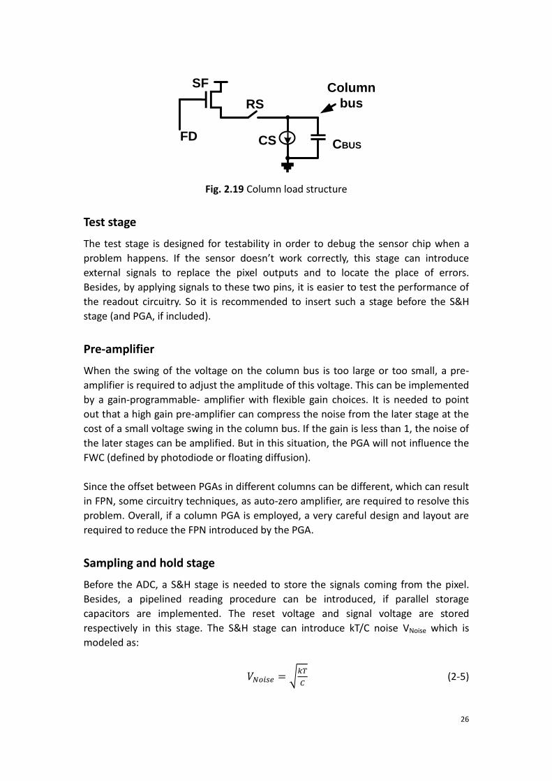
Figure 2.19 gives the model of the column load stage. The column bus parasitic
capacitance, CBUS, can be as large as 2 to 4pF. When the voltage of FD rises to a
higher level, the source follower can drive a current to charge the column bus.
However, when the voltage of column bus needs to decrease, a current source is
necessary to discharge the column bus capacitor. RS represents the row select
switch, SF is the source follower, CS is a current source. If the access time, t, of the
pixel is known, the value of current source can be calculated as:
𝐼 =𝐶𝐵𝑈𝑆𝑉
𝑡 (2-4)
where V is the largest voltage swing on column bus and t is the accessing time, CBUS is
column parasitic capacitance.
26
SF
CBUSCS
Column
busRS
FD
Fig. 2.19 Column load structure
Test stage
The test stage is designed for testability in order to debug the sensor chip when a
problem happens. If the sensor doesn’t work correctly, this stage can introduce
external signals to replace the pixel outputs and to locate the place of errors.
Besides, by applying signals to these two pins, it is easier to test the performance of
the readout circuitry. So it is recommended to insert such a stage before the S&H
stage (and PGA, if included).
Pre-amplifier
When the swing of the voltage on the column bus is too large or too small, a pre-
amplifier is required to adjust the amplitude of this voltage. This can be implemented
by a gain-programmable- amplifier with flexible gain choices. It is needed to point
out that a high gain pre-amplifier can compress the noise from the later stage at the
cost of a small voltage swing in the column bus. If the gain is less than 1, the noise of
the later stages can be amplified. But in this situation, the PGA will not influence the
FWC (defined by photodiode or floating diffusion).
Since the offset between PGAs in different columns can be different, which can result
in FPN, some circuitry techniques, as auto-zero amplifier, are required to resolve this
problem. Overall, if a column PGA is employed, a very careful design and layout are
required to reduce the FPN introduced by the PGA.
Sampling and hold stage
Before the ADC, a S&H stage is needed to store the signals coming from the pixel.
Besides, a pipelined reading procedure can be introduced, if parallel storage
capacitors are implemented. The reset voltage and signal voltage are stored
respectively in this stage. The S&H stage can introduce kT/C noise VNoise which is
modeled as:
𝑉𝑁𝑜𝑖𝑠𝑒 = √𝑘𝑇
𝐶 (2-5)

27
where k is the Boltzmann’s constant, T is the absolute temperature in kelvins and C is
the sampling capacitor. So a larger sampling capacitor introduces less noise to the
analog chain at the cost of longer sampling time.
ADC stage
The ADC is maybe the most critical component in the analog chain. A well-designed
ADC can introduce a smaller column FPN and can improve the efficient number of
bits (ENOB). Different structures are employed according to the requirements of
customers and applications. Generally, the ramp ADC, the successive approximation
ADC (SAR ADC) and the cyclic ADC are implemented most frequently. A comparison
of different column ADC designs is shown in table 2.1 [2.10]. MRMS means multiple-
ramp multiple-slope and MRSS represents multiple-ramp single-slope.
From the data mentioned in the table, it can be found that a single slope ADC is
preferred in combination with a smaller pixel pitch, a lower frame speed and a lower
power consumption application, while a cyclic ADC can provide the highest
conversion speed at the penalty of a larger area and a huge power consumption. SAR
seems like a trade-off between the sampling rate and the power consumption.
Tab. 2.1 Performance of the column level ADC [2.10]
Ref. ADC type Sampling rate (kHz)
Power/ADC (μW)
Area/ADC (μ𝑚2)
ENOB (bits)
DR (bits)
FOM (pJ/conversion)
[2.19] SAR 588 41 11088 12 n.a. 0.0170
[2.20] Cyclic 345 149 n.a. 12 19.8 0.1054
[2.21] Cyclic 435 300 n.a. 13 11.5 0.2380
[2.22] Cyclic 2000 430 88000 12 9.67 0.2631
[2.23] Single Slope
19.6 5.7 n.a. 10 n.a 0.2840
[2.24] Two Step Single Slope
250 112.5 n.a. 10 10.5 0.3169
[2.25] Single Slope
259.2 302.08 n.a. 12 11 0.5678
[2.26] Divide-by-two
2000 350.00 n.a. 8.2 n.a 0.5951
[2.27] SAR 414.72 297.62 n.a. 10 9.5 0.9854
[2.23] MRMS 81.3 95 n.a. 10 n.a 1.1411
[2.23] MRSS 64.6 95 n.a. 10 n.a 1.4361
[2.28] Single Slope
30.72 58.6 n.a. 11 10.2 1.6524
[2.29] SAR 200 234.375 n.a. 9 n.a 2.2888
[2.30] SAR 259.2 386.185 n.a. 10 8.84 3.2426
28
[2.23] Single Slope
19.3 77.5 n.a. 10 n.a 3.9214
[2.31] SAR 27.03 50 50400 8 n.a 7.2266
In this thesis, a single slope ADC is employed due to the relative small pixel pitch and
the limited reading speed. The details of the working principle and the design of it
will be introduced in chapter 4.
Except for the normal circuit noise, the ADC stage can introduce quantization noise
Vnoise modeled as:
𝑉𝑛𝑜𝑖𝑠𝑒 =𝑓𝑢𝑙𝑙−𝑠𝑐𝑎𝑙𝑒
2𝑁√12 (2-6)
where full-scale represents the largest swing of the input signals, N is the conversion
accuracy.
Digital Output stage
After the ADC, the digital signals are stored in column registers. Based on the total
number of parallel output channels, the number of columns in one group can be
obtained. Assuming the ADC provides 12 bit data, these 12 bit data will be read out
parallel through 12 reading buses at the same time. It should be noticed that the
columns in the same output channel are selected one by one. When the data in
every column are clocked out, the reading of one frame is completed. If digital
multiplexers are introduced, the parallel outputs can be converted to serial outputs,
which can reduce the number of output pins dramatically. In order to speed up the
reading process, LVDS (Low Voltage Differential Signaling) output drivers can be
employed.
Summary
In CMOS image sensors, one of the most critical design principles is to reduce column
FPN. For the analog readout circuitry, the offset between columns should be
minimized. To obtain a desired performance, careful layout is a significant issue,
which requires a large amount of experience and patience.
2.5. References
[2.1] Gene P. Weckler, “Operation of p-n Junction Photodetectors in a Photon Flux
Integration Mode” IEEE Journal of Solid-state Circuits, Vol. SC-2, NO.3, page
65-73, September 1967.
[2.2] Noble, P.J.W, “Self-scanned silicon image detector arrays” Electron Devices,
IEEE, page 202–209, April 1968.
[2.3] Chamberlain, S.G., “Photosensitivity and Scanning of Silicon Image Detector

29
Arrays” IEEE Journal of Solid-state Circuits, Vol.4 page 333-342, December
1969.
[2.4] Spyros Kavadias etc. “A Logarithmic Response CMOS Image Sensor with On-
Chip Calibration” IEEE Journal of Solid-state Circuits, Vol.35, NO.8, page
1146-1152, August 2000.
[2.5] Markus Loose etc. “A Self-Calibrating Single-Chip CMOS Camera with
Logarithmic Response” IEEE Journal of Solid-state Circuits, Vol.36, NO.4,
page 586-596, April 2001.
[2.6] S. Sugawa etc. “A 100dB Dynamic Range CMOS Image Sensor Using a Lateral
Overflow integration capacitor” in IEEE int. Solid-State Circuits Conf. (ISSCC)
Dig. Tech. Paper, page 352-353, February 2005.
[2.7] Nana Akahane etc. “A Sensitivity and Linearity Improvement of A 100-dB
Dynamic Range CMOS Image Sensor Using a Lateral Overflow Integration
Capacitor” IEEE Journal of Solid-state Circuits, Vol.41, NO.4, page 851-858,
April 2006.
[2.8] Noriko Ide etc. “A Sensitivity and Linearity Improvement of a 100-dB
Dynamic Range CMOS Image Sensor Using a Lateral Overflow Integration
Capacitor” IEEE Journal of Solid-state Circuits, Vol.43, NO.7, page 1577-1587,
July 2008.
[2.9] Mitsuhito Mase etc. “A Wide Dynamic Range CMOS Image Sensor With
Multiple Exposure-Time Signal Outputs and 12-bit Column-Parallel Cyclic
A/D Converters” IEEE Journal of Solid-state Circuits, Vol.40, NO.12, page
2787-2795, December 2005.
[2.10] Cheng Ma “PIXEL ADC DESIGN FOR HYBRID CMOS IMAGE SENSORS”, Master
thesis, Delft University of Technology, page 30-31, August, 2010,.
[2.11] Richard Hornsey “Design and Fabrication of Integrated Image Sensor”, page
76.
[2.12] Richard Hornsey “Design and Fabrication of Integrated Image Sensor”, page
103.
[2.13] Richard Hornsey “Design and Fabrication of Integrated Image Sensor”, page
105.
[2.14] Theuwissen, A., CMOS image sensors: State-of-the-art. Solid State
Electronics, 52(9): page 1401-1406, 2008.
[2.15] I. Takayanagi etc. “A 600×600 Pixel, 500 fps CMOS Image Sensor with a
4.4μm Pinned Photodiode 5-Transistor Global Shutter Pixel”,
INTERNATIONAL IMAGE SENSOR WORKSHOP, Ogunquit Maine, USA, 2007.
[2.16] http://www.sony.net/SonyInfo/News/Press/200806/08-069E/index.html,
June, 2012.
[2.17] http://www.imaging-resource.com/news/2012/01/23/sony-next-gen-
sensors-improve-resolution-low-light-shooting, June, 2012.
[2.18] http://www.teledynedalsa.com/mv/knowledge/globalshutter.aspx, June,
2012
[2.19] Matsuo, S. etc. “8.9-Megapixel Video Image Sensor With 14-b Column-
Parallel SA-ADC”, IEEE Transactions on Electron Devices, Vol. 56, page 2380-

30
2389, November2009.
[2.20] Mase, M., etc. “A wide dynamic range CMOS image sensor with multiple
exposure-time signal outputs and 12-bit column-parallel cyclic A/D
converters” IEEE Journal of Solid-State Circuits, Vol. 40, NO.12, page 2787-
2795, December, 2005.
[2.21] Park, J. etc. “A High-Speed Low-Noise CMOS Image Sensor with 13-b
Column-Parallel Single-Ended Cyclic ADCs” IEEE Transactions on Electron
Devices, Vol. 56, page 2414-2422, November2009.
[2.22] Furuta, M. etc. “A High-Speed, High-Sensitivity Digital CMOS Image Sensor
With a Global Shutter and 12-bit Column-Parallel Cyclic A/D Converters” IEEE
Journal of Solid-State Circuits, Vol. 42, NO.4, page 766-774, April, 2007.
[2.23] Snoeij, M. “Analog Signal Processing for CMOS Image Sensors” PhD thesis,
Delft University of Technology, 2007, ISBN: 978-90-9022129-8.
[2.24] Lim, S., etc. “A High-Speed CMOS Image Sensor with Column-Parallel Two-
Step Single-Slope ADCs” IEEE Transactions on Electron Devices, Vol. 56, page
393-398, March, 2009.
[2.25] Nitta, Y. etc. “High-speed digital double sampling with analog CDS on
column parallel ADC architecture for low-noise active pixel sensor” IEEE
ISSCC Dig. Tech. Papers, page 500-501, 2006.
[2.26] Lee, J. etc. “A/D Converter using Iterative Divide-by-Two Reference for CMOS
Image Sensor” in SoC Design Conference, ISOCC '08. International, page 35-
36, 2008.
[2.27] Krymski, A. etc. “A high-speed, 240-frames/s, 4. 1-Mpixel CMOS sensor” IEEE
Transactions on Electron Devices, Vol.50, page 130-135, January, 2003.
[2.28] Findlater, K. etc. “SXGA pinned photodiode CMOS image sensor in 0.35 μm
technology” IEEE ISSCC Dig. Tech. Papers, page 218-219, 2003.
[2.29] Mansoorian, B. etc. “A 250 mW, 60 frames/s pixel 9 b CMOS
digital imagesensor” IEEE ISSCC, Digest of technical papers, page 312-313,
1999.
[2.30] Takayanagi, I. etc. “A 1.25 inch 8.3 M pixel digital output CMOS APS for UDTV
application” Proc. ISSCC 2003, page216-217, 2003.
[2.31] Zhou, Z. etc. “CMOS active pixel sensor with on-chip successive
approximation analog-to-digital converter” IEEE Transactions on Electron
Devices, Vol. 44, page 1759-1763, October, 1997.

31
Chapter 3 Design of a 6T dual transfer gates high dynamic range
pixel
3.1. Specifications of image sensor
Before designing a pixel, it is important to know the image sensor specifications. As a
semiconductor device, an image sensor has its typical parameters, such as
conversion gain, full well capacity, fill factor, resolution etc. At the same time, as a
sensor device that has to convert the physical world value to digital signals, it also
has the common parameters related to signal processing field, such as dynamic
range, SNR, power consumption etc. The combination of these important parameters
is a description of the quality of the image sensor.
3.1.1. Conversion gain
Conversion gain (CG) is defined as the of voltage variation caused by one electron at
the conversion node. Obviously, CG is related to the conversion node capacitance.
𝐶𝐺 =𝑞
𝐶𝑛𝑜𝑑𝑒 (3-1)
where q is the charge of one electron and Cnode is the total capacitance of the
conversion node. In fact, CG can also be defined as the variation in digital number at
the output for 1 electron at the conversion node.
3.1.2. Full well capacity
FWC is the abbreviation of full well capacity and it can be used to describe the
maximum amount of electrons generated and stored in the photodiode. It is
significant to notice that the pixel FWC is determined by the smaller one of the
photodiode charge capacity and the FD charge capacity (if a transfer gate is
implemented). If the FWC is limited by the photodiode, the maximum signal swing at
the FD can be calculated as:
𝑆𝑖𝑔𝑛𝑎𝑙 𝑆𝑤𝑖𝑛𝑔 =𝐹𝑊𝐶×𝑞
𝐶𝑛𝑜𝑑𝑒
= 𝐹𝑊𝐶 × 𝐶𝐺 (3-2)
where q is the electron charge, cnode represents the FD capacitance and CG is the

32
conversion gain. This formula is effective when the largest signal swing at the FD is
not limited by the supply voltage or other factors.
3.1.3. Signal to noise ratio
Signal to noise ratio (SNR) is nearly the most frequently mentioned parameter in
CMOS circuitry design when quantifying the quality of a device. It describes the
maximum ratio of signal power to noise power in a given system. In an image sensor,
the maximum SNR is achieved when the photodiode reaches the edge of saturation.
It is expressed as:
𝑆𝑁𝑅 = 20 log (𝑁𝑠𝑖𝑔𝑛𝑎𝑙
𝑁𝑛𝑜𝑖𝑠𝑒) [𝑑𝐵] (3-3)
where Nsignal represents the number of signal electrons and the Nnoise is the number
of noise electrons.
3.1.4. Dynamic range
One of the key parameters in an image sensor is the dynamic range. It is defined as
the ratio between pixel saturation level and noise floor in dark. In general, the
saturation level is determined by FWC of pixel, and the smallest illumination intensity
that can be handled is limited to the noise floor. DR can be calculated as:
𝐷𝑅 = 20log (𝑁𝑠𝑎𝑡
𝑁𝑑𝑎𝑟𝑘) [dB] (3-4)
where Nsat is the amount of electrons collected by pixel at saturation level, while Ndark
represents pixel noise level without illumination[in electrons]. Hence, to increase the
dynamic range, two main paths can be taken into account. One is to increase the
FWC of photodiode and the other is to decrease the noise floor.
Generally, a high dynamic range is preferred in various applications, especially when
a part of the object is bright and the other part is dark. It directly influences the
maximum contrast, a significant parameter to describe the performance of cameras.
3.1.5. Fill factor
The fill factor (FF) is defined as the ratio between the pixel light sensitive area and
the total pixel area. A single pixel can detect incident light in a certain area which is
usually smaller than the square of pixel pitch. In a traditional image sensor, most of
the time, the pixel area is partially covered by the metal routing used for the
transistors inside the pixel. In some applications, micro lenses are introduced to
improve fill factor. In fact, a relative higher fill factor in CCD is an important reason

33
why CCD sensors still have some advantages over CMOS imagers. Besides, the fill
factor is tightly related to the light sensitivity of pixel. A higher fill factor is especially
preferred in low illumination environment in order to achieve a better sensitivity.
3.1.6. Resolution
General consumers always want the resolution of cameras to be higher and higher.
The update has been achieved from 0.3M (first generation cellphone camera) to 2M,
to 5M (a main stream resolution nowadays) to, 8M, to 12M, to 41M (Nokia’s latest
cellphone model 808 PureView) [3.7]. Though in a professional view higher
resolution doesn’t equal to higher performance, resolution is still a quick and easy
parameter to describe the property of digital cameras. The reason is lower quantum
efficiency and more crosstalk in small pixels. Resolution shows how many pixels are
integrated in a single chip. Generally speaking, more pixels mean more details of the
object can be exhibited in playback. Besides, if the pixel pitch is also known, the
optical size of the sensor can be defined.
3.1.7. Power consumption
No matter when the performance of an integrated circuit chip is mentioned, power
consumption is an important parameter. In an image sensor chip, most of the power
consumption is consumed by the readout electronics, including for example, the
analog chain, the ADC, the output driver, the signal processing etc.
3.2. Noises in CMOS image sensor
Noise exists in any type of integration circuit, which leads to a limited SNR. In the
image sensor field, noise in the readout circuitry sets the fundamental limit under
the condition of low illumination, while the photodiode shot noise is the dominant
noise source at high illumination. Besides, a special type of noise, FPN (fixed-pattern-
noise), exists in an image sensor system. It can result in a spatial noise which is very
sensitive to human eyes. Figure 3.1 shows the difference of these two type noises.
Frame
Output
Pixel 1
Pixel 2
All the outputs are obtained
under same conditions
FPN
Temporal
noise
Fig. 3.1 Temporal noise and Fixed-pattern-noise

34
The output difference (taken in different frames under the same conditions) in the
same pixel is defined as temporal noise, while the output difference (taken in the
same frame under the same conditions) in different pixels is defined as fixed-pattern-
noise.
3.2.1. Temporal noise
In a CMOS active pixel (APS), several noise sources make a contribution to the
temporal noise. These noise sources mainly include the kT/C noise from the reset
action, flicker and thermal noise from the source follower, noise from the readout
circuitry (including quantization noise in the A/D conversion) and photon shot noise
under illumination. The figure 3.2 plots the general components of noise existing in
an imager system and their relative magnitude. It should be noticed that the
maximum SNR is achieved at the point where electrons in pixel reach saturation. It is
because the signal is proportional to the number of electrons generated by the
incident light and the photon shot noise is proportional to the square root of the
number of electrons generated by the incident light.
Photon shot noise
Photon shot noise is a type of noise related to the random arrival of photons. Hence,
it is related to a nature physical process other than pixel design or fabrication
technology, leading to an inherent noise source. In fact, photon shot noise dominates
the noise performance under high illumination levels. Due to its direct relationship
with illumination level guaranteed by a physical law, the photon shot noise can be
calculated easily.
Ideal signal
response
Photon shot noiseADC quantization noise Constant noise (1/f, thermal etc.)
Total noise
SNR
DR
Light intensity [log]
Se
ns
or
ou
tpu
t [l
og
]
Imax Imin
Constant noise
dominatePhoton noise dominate
Fig. 3.2 Noise in CMOS image sensor [3.6]

35
Reset noise
Before the start of an integration, the photodiode and the floating diffusion need to
be reset to a certain voltage level. During this process, a voltage is sampled to the
related capacitor, which leads to reset noise. This sampling noise is normally referred
to “kTC” noise in any analog circuitry. The fundamental source of this reset noise is
the thermal noise of the reset switch implemented by an nMOS transistor. During
sampling, the nMOS transistor can be treated as a switch which could introduce
thermal noise into system. It can be calculated as:
𝑉𝑛𝑜𝑖𝑠𝑒̅̅ ̅̅ ̅̅ ̅
,𝑅𝑀𝑆= √𝑘𝑇 𝐶𝑝𝑑⁄ (3-5)
where k is the Boltzmann constant, T is the absolute temperature in kelvins, and CPD
is the capacitance of photodiode. An efficient method to eliminate reset noise is to
apply correlate double sampling (CDS) technology. Before charge transfer (pinned
photodiode pixel), the reset voltage is firstly read out and stored in a S&H circuit.
Afterwards, the signal voltage (contains reset noise) is also sampled and stored in a
S&H stage. Only the difference between these two signals will be converted to digital
signals.
1/f noise
1/f noise (also called flicker noise or low-frequency noise sometimes) refers to the
noise whose power spectral density is inversely proportional to the frequency. With
the development of CMOS technology, the dimensions of the MOS transistors
become smaller and smaller, which results in 1/f noise playing a more important role
in the discussion around temporal noise. Unfortunately, until now no agreed
universal mathematical or physical model can be used to calculate it. Generally, in
MOS transistors, two main theories of flicker noise were modeled, knowing as the
carrier number fluctuation theory and the mobility fluctuation theory. A detailed
analysis of 1/f noise in CMOS image sensor can be found in [3.1]. For simplicity, an
approximate model could be built as:
𝑉𝑛𝑜𝑖𝑐𝑒2̅̅ ̅̅ ̅̅ ̅ =
𝐾
𝐶𝑂𝑋𝑊𝐿×
1
𝑓 (3-6)
where K is a process dependent parameter, COX is gate capacitance and W and L are
transistor dimensions. It is evident that 1/f noise becomes larger in a more advanced
process technology (smaller minimum lithography dimensions and consequently
smaller transistor dimensions). Undoubtedly, more effort is still needed to research
this fundamental noise source in electronic devices. It is necessary to point out that
part of the flicker noise (frequency below sampling rate) can be eliminated by the CDS
circuitry [3.2].

36
3.2.2. Fixed pattern noise
Compared to temporal noise, FPN (fixed pattern noise) is a space-dependent noise,
in fact an offset between pixels. It doesn’t vary from frame to frame. FPN is referred
to the variation of output from different pixels under same illumination conditions.
As a two-dimensional device, image sensor suffers from pixel and column level FPN
simultaneously. The former is mainly due to mismatch of in-pixel transistors, while
the mismatch of column level readout circuitry dominates the latter type of FPN.
Pixel level FPN can be caused by the variation of the transistor threshold voltage
between pixels. The main advantage of CCD over CIS is less FPN, because a relative
simpler pixel structure and a global analog readout structure with an off-chip ADC
were implemented in CCD imagers. By employing a double sampling technology,
pixel level FPN is easy eliminated.
Column FPN is caused by different offset between the columns. In fact, human eyes
are more sensitive to column stripes than to pixel level offset. Compared to pixel
FPN, column FPN is not easy to be removed by circuitry methods, and it is generally
solved by digital methods. Figure 3.3 (a) shows an image with serious pixel level FPN
and figure 3.3 (b) is the same image but the pixel FPN is eliminated. Figure 3.4 gives
an example of the influence of column FPN in a photo.
Fig. 3.3 (a) A family of polar-bears with Fig. 3.3 (b) The fixed pattern noise
pixelized fixed-pattern-noise was subtracted from the image [3.9]
According to the illumination conditions, two other parameters are introduced to
evaluate the quality of image sensor. They are the PRNU (photo-response non-
uniformity) and the DSNU (dark-signal non-uniformity). PRNU and DSNU are
measured under illumination and dark environment respectively. The relationship
between FPN, PRNU and DSNU can be described as figure 3.5. The difference in
slopes,α andβ , reflects the photo-response non-uniformity (if the outputs are
obtained under same illumination and the DSNU is subtracted from the response) or
the dark-signal-non-uniformity (if both of the outputs are obtained without
illumination). The output difference of pixel 1 and pixel 2 at zero exposure time is the

37
fixed-pattern-noise in dark. It is necessary to point out that the PRNU plays the main
role under illumination and is much larger than DSNU. However, to obtain an
accurate PRNU value, the DSNU needs to be subtracted from the original image data
before calculating PRNU [3.4]. Because the PRNU represents the gain difference
between pixels under illumination, its absolute value should be proportional the
exposure time. In fact, PRNU mostly is expressed in % and that makes it independent
of the exposure time
Fig. 3.4 Column FPN in image [3.3]
Exposure time
Output [V]
α
βFPN
Pixel 1
Pixel 2
Fig. 3.5 Difference of FPN, PRNU and DSNU
3.3. The pixel design
In section 2.3, three traditional categories of high dynamic range pixels are
introduced. In this thesis, another dynamic-range-enhanced pixel architecture
reported in [3.5] is implemented based in 110nm CMOS image sensor technology. It
involves two transfer gates and two floating diffusion nodes to improve the
performance in both low and high illumination environment. The details of the
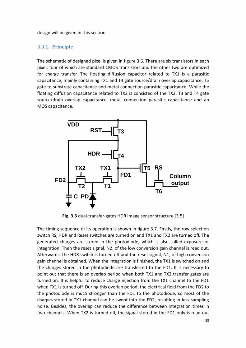
38
design will be given in this section.
3.3.1. Principle
The schematic of designed pixel is given in figure 3.6. There are six transistors in each
pixel, four of which are standard CMOS transistors and the other two are optimized
for charge transfer. The floating diffusion capacitor related to TX1 is a parasitic
capacitance, mainly containing TX1 and T4 gate source/drain overlap capacitance, T5
gate to substrate capacitance and metal connection parasitic capacitance. While the
floating diffusion capacitance related to TX2 is consisted of the TX2, T3 and T4 gate
source/drain overlap capacitance, metal connection parasitic capacitance and an
MOS capacitance.
RS
Column
output
PD
T1
T4
T5TX1
T6
T3RSTVDD
FD1
T2
TX2
HDR
C
FD2
Fig. 3.6 dual-transfer-gates HDR image sensor structure [3.5]
The timing sequence of its operation is shown in figure 3.7. Firstly, the row selection
switch RS, HDR and Reset switches are turned on and TX1 and TX2 are turned off. The
generated charges are stored in the photodiode, which is also called exposure or
integration. Then the reset signal, N2, of the low conversion gain channel is read out.
Afterwards, the HDR switch is turned off and the reset signal, N1, of high conversion
gain channel is obtained. When the integration is finished, the TX1 is switched on and
the charges stored in the photodiode are transferred to the FD1. It is necessary to
point out that there is an overlap period when both TX1 and TX2 transfer gates are
turned on. It is helpful to reduce charge injection from the TX1 channel to the FD1
when TX1 is turned off. During this overlap period, the electrical field from the FD2 to
the photodiode is much stronger than the FD1 to the photodiode, so most of the
charges stored in TX1 channel can be swept into the FD2, resulting in less sampling
noise. Besides, the overlap can reduce the difference between integration times in
two channels. When TX2 is turned off, the signal stored in the FD1 only is read out

39
first. This signal is a combination of the reset noise and the detected signal in high
gain channel, referred to N1+S1. Finally, the HDR switch is turned on to obtain the
total signal stored in the FD1 and the FD2, referred to N2+S2.
The FWC is limited by the photodiode capacitance or FD2 capacitance in this
structure. There are two conversion gains related to FD1 and FD2 respectively. FD1,
where signal N1+S1 is stored, is called high gain channel and the other channel
(FD1+FD2) is defined as the low gain channel designed for high illumination
condition. In fact, two individual readout chains are required to process these two
reading events. The high conversion gain related readout chain owns a high gain
column pre-amplifier, which can reduce amplifier input referred noise, in order to
improve sensitivity in low illumination. A low gain column pre-amplifier is
implemented in the low conversion gain channel to avoid saturation in high
illumination. Through the processing of these two readout chains separately, the
dynamic range can be extended by re-constructing the image based on the signals
from these two channels. Another advantage by implementing two readout chains is
a higher frame rate when applying a pipelined read out method. Otherwise, only one
programmable-gain-amplifier is enough to finish the four reading process (two resets
and two signals). The details of the readout chain design will be explained in chapter
4.
RST
HDR
TX1
TX2
RS
N2 N1 N1+S1 N2+S2
Fig. 3.7 Timing sequence of the pixel [3.5]
3.3.2. Layout considerations
For the pixel design, most of the challenges are related to the layout, because the
available area is very limited and precious. Obviously, the performance of the image
sensor is strongly depended on the pixel layout. In figure 3.8, an example of a cross
section view of a pinned PD is shown.
The most significant progress different from regular photodiodes is the
implementation of a p+ layer beyond photodiode. This layer can screen the surface
defects from the photodiode. The idea of the pinned layer is coming from the CCD

40
image sensors and introducing of p+ layer is aiming to increase the quantum
efficiency in blue light region. It can be explained by the effect of the additional pn
junction near the surface, which can collect the electrons generated by the short
wavelength lights absorbed in relative shallower region. It is important that the n-
layer of the photodiode should be more close to the transfer gate than the pinned p+
layer. Otherwise, it is difficult to transfer the charges stored in the PD to the floating
diffusion node because of a potential barrier.
epi-p
TX
FD
+p
-n
+n
Fig. 3.8 Cross section of pinned photodiode
Photodiode and transfer gates shape
As introduced above, two transfer gates are employed in this pixel. So, first of all, it is
important to decide the locations where these two transfer gates are placed.
Generally, the following plans, shown in figure 3.9 and figure 3.10, can be employed.
Photodiode
TX1
TX2
Photodiode
TX1 TX2
Fig. 3.9 Two TXs in one side Fig. 3.10 Two TXs in different sides
But in the case of a relative small pixel pitch, both of them are not an optimized
proposal. For the right one, two transfer gates horizontally placed in one side have a
potential problem that when one TX is turned on, it is difficult to transfer the charges
stored in the corner behind the other transfer gate. The reason for this is that the
electrical field is blocked off by the transfer gates, leading to an image lag which is

41
very harmful to the image quality. The problem becomes more evident when the
previous frame is bright and the next frame is bark, in which situation the later frame
may become gray. For the left plan, there will be a metal line (used to connect n-well
capacitance to the HDR transistor) across the pixel, which can cause a considerable
decrease of the fill factor in such a small pixel pitch.
In order to solve the problem existing in above structures, the following design,
shown in figure 3.11, is implemented. In such a shape, the transfer gates are placed
in the same side corners of photodiode. Now, the electrical field is continuous within
the photodiode.
Photodiode
TX1 TX2
Fig. 3.11 Two TXs placed in same side corns
Implementation of MOS capacitor
Obviously, the photodiode area should be as large as possible in the given pixel pitch.
However, another component, the dynamic-range enhanced capacitor, should also
be taken into account when doing the design. A preliminary prediction shows the
photodiode area is around 12𝜇𝑚2. Since the applied CMOS image sensor technology
is a new one, the electron density within the photodiode can only be estimated
based on the experience. An electron density of 4500𝑒−/𝜇𝑚2 is assumed in this
design. The required capacity of the total FD1+FD2 capacitor can be estimated by the
following formulas:
𝑄 = 𝑁 × 𝑞 (3-7)
𝐶 = 𝑄 𝑉⁄ (3-8)
where N is the maximum amount of electrons collected by the photodiode and q is
the electron charge constant. In this design, a 1.6V voltage swing is acceptable. By
these conditions, the capacity of required capacitor can be calculated.
The calculation result shows C is about 5.4fF. The gate to substrate capacitance is
approximately 4.722×10⁻³(F/m2). It should be noticed that the calculated capacitance
contains the parasitic capacitances of the FD1 and the FD2 as well. So the true area
of the MOS capacitor is smaller than the calculated value. The final parameters of the
related capacitance and area in the real design will be provided in the section 3.4.

42
Metal connections
In pixel design, the total length of the metal connections should be as short as
possible because, except for the photodiode, the area uncovered by metals can also
absorb photons and generate hole-electron pairs. In fact, the fill factor is actually
limited by vertical and horizontal metal lines within the pixel array. Because of the
thickness of the metal lines and the vertical distance between various metals, the
reflection of the incident light cannot be ignored. Figure 3.12 gives a bad example of
metal connections around photodiode. From the figure, it can be noticed that a
relative large part of incident lights is reflected or rejected by the metals, leading to a
smaller effective sensitive area. As a comparison, the metal lines in figure 3.13 are
organized much more ordered, and it could make the light sensitive area much larger.
Hence a higher fill factor is promised and clearly a better performance could be
expected. So it is better to place the higher layer metal farther from photodiode. For
optimized performance, all the metal lines should be placed as far as possible away
from the photodiode to obtain a large fill factor.
Another problem related to the metal connection is the metal covering capacitance
which contributes a large part to the floating diffusion capacitance. Huge patience
and effort are necessary during the layout of metal connections, especially at the
location of the FD1, aiming to reduce the parasitic metal covering capacitance.
Photodiode
M2
M1
M3
M4
Photodiode
M2
M1
M3
M4
Fig. 3.12 Poor metal connections Fig. 3.13 Optimized metal connections
Floating diffusion
As introduced in the previous chapter, the floating diffusion node is the place to store
the charges transferred from the photodiode. Like the PD, the floating diffusion is
also sensitive to incident light and can generate hole-electron pairs, which can be
treated as a noise source. So it should be shielded from light by metal coverage.
Besides, aiming to provide a dynamic range as large as possible, the layout of the FD1
should be very carefully done. In fact, there is a trade-off between potential image
lag risk and high conversion gain. In order to achieve a high CG, the FD1 capacitance
should be minimized. However, the gate to source/drain overlap capacitance of the
43
transfer gate is proportional to the width of the transfer gate. In addition, the active
to substrate capacitance has a relationship with active area and perimeter. But the
risk of image lag increases with the decrease of the effective transfer gate width.
During layout work, it is found that an optimized metal layout can improve the
conversion gain over 15% (which can influence the dynamic range directly) in
comparison to a poor layout.
The combination of individual pixel layout
Except for the tips mentioned above, a careful calculation and prediction for the
relative location and distance of adjacent pixels are necessary in the layout of the
pixel array. A 4.8μm pixel pitch means the spatial period of pixel array is 4.8μm both
in vertical and horizontal axis. The separation of VDD and VGND is also
recommended to avoid the potential short circuit due to defects (such as metal
particles) in production. The short between VDD (VGND) and the column causes only
one column failure, but if the VDD is short to VGND, the whole chip is destroyed,
causing a decrease of the yield. In fact, in some applications, the loss of several rows
or columns can be tolerated and these losing signals can be restructured by digital
processing, like an interpolation method. So in this design, the column bus is laid
between VDD and VGND to increase the yield. Figure 3.14 shows the details of a
single pixel and in figure 3.15 is a three by three pixel layout shown, which can check
the compliance to the design rules of the pixel array. Because the image signals are
read out row by row, the control lines are implemented horizontally and column and
power lines are laid vertically.
Fig. 3.14 Single pixel layout Fig. 3.15 3×3 pixel layout
3.4. Parameters estimation and calculation
Fill factor
The fill factor is limited by the metal connections as analyzed in a previous section of
this chapter. The available incident light window in this design is 3.80μm ×3.42μm.

44
Since the pixel pitch is 4.8μm × 4.8μm, the predicted fill factor is 56.4%.
Full well capacity
The photodiode area is approximately 11.5𝜇𝑚2 and the prediction of electrons
density within photodiode is 4500𝑒− 𝜇𝑚2⁄ . It is necessary to point out that this value
is an assumption under the condition of 1V pinned voltage (so the minimum FD
voltage during the transfer should be larger than this value to ensure completely
charge transfer). Full well capacity is calculated as followers:
𝐹𝑊𝐶 = 𝐴𝑟𝑒𝑎 (𝑝ℎ𝑜𝑡𝑜𝑑𝑖𝑜𝑑𝑒) × 𝐸𝑙𝑒𝑐𝑡𝑟𝑜𝑛𝑠 𝑑𝑒𝑛𝑠𝑖𝑡𝑦
= 51750 𝑒−
As introduced in previous section, the FWC is an important parameter for an image
sensor, especially for HDR applications. This value will be used throughout the
following calculation.
Conversion gain
The calculated FD1 and FD2 capacitances are shown in table 3.1. According to these
parameters, the conversion gains of high gain and low gain channels can be obtained.
Tab. 3.1 Capacitance of related items
FD1 cap Unit (fF) FD2 cap Unit (fF)
TX1(TX2) overlap cap 0.196 0.281 HDR (+Reset) overlap cap 0.059 0.118 Active area cap 0.359 0.383 Active lateral cap 0.286 0.323 Source follower gate cap* 0.150 0 MOS cap 0 1.596 Metal covering cap 0.49 1.14 Total cap 1.540 3.841
* This value is 1/3 of the calculated gate to substrate capacitance, because source
follower works in saturation model and the electron channel is pinched off.
The floating diffusion capacitances related to high gain and low gain channel are FD1
and FD1+FD2 respectively:
𝐶𝐺(𝐻𝑖𝑔ℎ 𝑔𝑎𝑖𝑛) =𝑞
𝐶𝐹𝐷1=
1.6 × 10⁻¹⁹𝐶
1.54 × 10⁻¹⁵𝐹= 103.89𝜇𝑉/𝑒−
𝐶𝐺(𝐿𝑜𝑤 𝑔𝑎𝑖𝑛) =𝑞
𝐶𝐹𝐷1+𝐹𝐷2=
1.6 × 10⁻¹⁹𝐶
5.381 × 10⁻¹⁵𝐹= 29.73𝜇𝑉/𝑒−
In the low conversion gain channel, the total floating diffusion capacitance is 5.38fF,
which matches the calculated value (5.4fF in the section 3.4: Implementation of MOS

45
capacitor) well. Indeed, the threshold voltage of the reset transistor is about 0.6V, so
the maximum FD reset voltage is 2.7V. As the electron density is estimated under the
assumption that the pinned voltage is 1.0V, the minimum FD voltage should be larger
than this value. Otherwise, the electrons stored in photodiode cannot be transferred
to floating diffusion node completely. Therefore, the assumption of 1.6V (1.6V<2.7V-
1.0V) voltage swing on FD is reasonable.
Source follower noise
An important part of the system noise is contributed by source follower. This noise is
usually transferred to the pixel noise through conversion gain. So except for the
advantages mentioned above, a higher conversion gain can reduce the equivalent
pixel noise. To simulate this noise, the column bus parasitic capacitance should be
firstly extracted. This capacitance mainly contains metal covering capacitance, gate to
drain/source overlap capacitance (selection switch) and active to substrate
capacitance. The related parameters are given in table 3.2.
The distributed pixel access time (the time used to transfer the signals from the pixel
to the column bus) is 2.5μs in this design. In the design, the column biasing current
source has a value of 2.5μA, which is obtained by simulation. The simulation scheme
and the speed of the charging and discharging are given in figure 3.16 and 3.17
respectively.
Vin
2.7VVcolumn
2.5pF
W/L=0.3/0.325
2.5uA
Fig. 3.16 Column biasing current source simulation scheme
It can be concluded that the 2.5μA current source can completely discharge the
column capacitance in 2.5μs pixel accessing time. The following noise simulation is
based on such a current value.
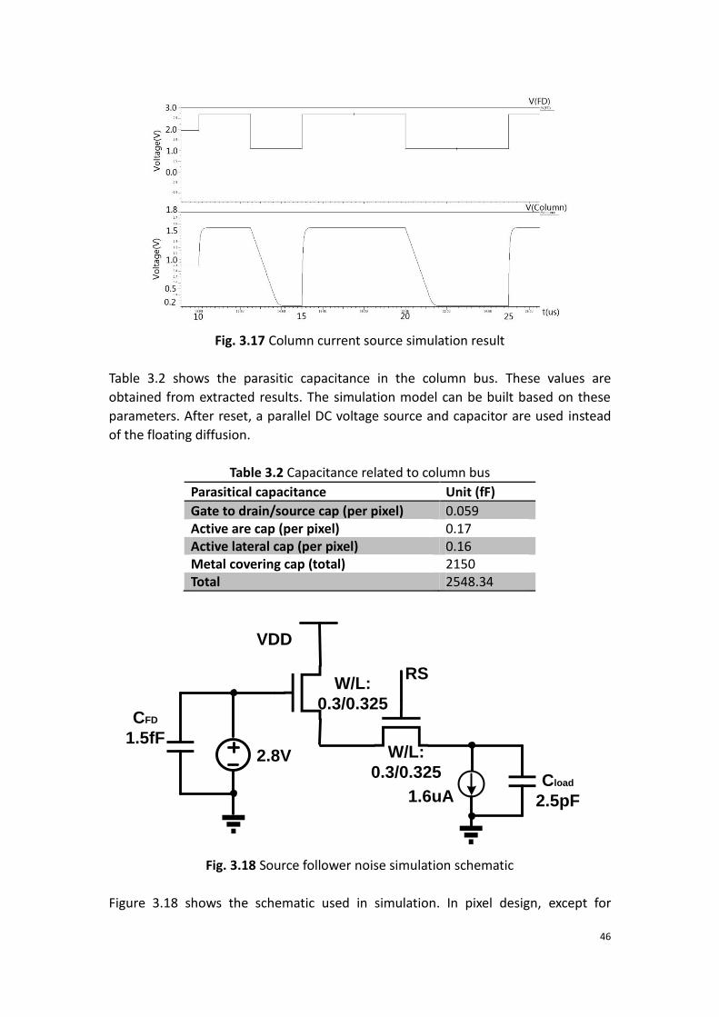
46
Fig. 3.17 Column current source simulation result
Table 3.2 shows the parasitic capacitance in the column bus. These values are
obtained from extracted results. The simulation model can be built based on these
parameters. After reset, a parallel DC voltage source and capacitor are used instead
of the floating diffusion.
Table 3.2 Capacitance related to column bus
Parasitical capacitance Unit (fF)
Gate to drain/source cap (per pixel) 0.059 Active are cap (per pixel) 0.17 Active lateral cap (per pixel) 0.16 Metal covering cap (total) 2150 Total 2548.34
VDD
RS
2.8V
CFD
1.5fF
Cload
2.5pF1.6uA
W/L:
0.3/0.325
W/L:
0.3/0.325
Fig. 3.18 Source follower noise simulation schematic
Figure 3.18 shows the schematic used in simulation. In pixel design, except for

47
transfer gates, all the transistors have the same dimensions: W=0.3 μ m and
L=0.325μm. The DC voltage of the FD is set to 2.7V, because the noise analysis is
performed under dark environment.
Figure 3.19 shows the 3dB-bandwidth, 1.79MHz, of the source follower. It is used to
determine the interval of the noise integration. The relationship between signal
bandwidth and noise bandwidth is:
𝐵𝑊𝑁𝑜𝑖𝑠𝑒 =𝜋
2∙ 𝐵𝑊𝑆𝑖𝑔𝑛𝑎𝑙 (3-9)
Hence the noise bandwidth is around 2.81MHz. Besides, the source follower has a
gain of -1.3dB(×0.86).
Fig. 3.19 AC response of source follower
The simulated input referred noise curve is shown in figure 3.20. Then the RMS input
noise can be calculated based on the following formula:
𝑁𝑜𝑖𝑠𝑒𝑆𝐹,𝑖𝑛𝑝𝑢𝑡 = √∫ 𝑉𝑛𝑜𝑖𝑠𝑒2
𝐵𝑊𝑛𝑜𝑖𝑠𝑒
1
𝑑𝑓 = 320μV
where NoiseSF,input represents the source follower RMS input referred noise, BWnoise is
the noise bandwidth and the Vnoise is the noise in the unit of 𝑉 √𝐻𝑧⁄ , which is
obtained from the simulation results.

48
Fig. 3.20 Input referred noise of source follower
This noise can be transferred to an equivalent pixel noise through the conversion
gain. As calculated above, the high gain channel has a CG of 103.89μV 𝑒−⁄ , the
equivalent pixel noise with the high conversion gain is:
𝑁𝑜𝑖𝑠𝑒𝑝𝑖𝑥𝑒𝑙,𝑒𝑞𝑢𝑖. =𝑁𝑜𝑖𝑠𝑒𝑆𝐹,𝑖𝑛𝑝𝑢𝑡
𝐶𝐺= 3.1𝑒− [in electrons]
where Noisepixel,equi. represents the equivalent pixel noise, and CG is the conversion
gain of the high gain channel. It should be noticed that the noises source outside of
the pixel are not taken into account. The complete noise analysis and calculation of
the whole readout chain is given in chapter 4.
3.5. Photon transfer curve
To get the optimized column gain setting, the PTC (photon transfer curve) needs to
be simulated. In this section, a detail calculation for the column gain setting will be
given.
The first step is to determine the PTC of the low gain channel. The column gain is
determined by the pixel output swing and the column PGA input and output swing.
Pixel output swing is:
𝑃𝑖𝑥𝑒𝑙 𝑜𝑢𝑡𝑝𝑢𝑡 𝑠𝑤𝑖𝑛𝑔 = 𝐹𝑊𝐶 × 𝐶𝐺(𝑙𝑜𝑤 𝑔𝑎𝑖𝑛) × 𝐺𝑎𝑖𝑛(𝑆𝐹)
= 1.32V
The maximum available input and output swing of column PGA is 2V and 1.5V
respectively. Hence, the column gain for low conversion gain channel is ×1.13.
Corresponding to such a gain, the input referred noise of PGA is 120.2μV. These

49
values (PGA swings and PGA input referred noise) are obtained from the design of
X. Ge. The total pixel noise is calculated as:
𝑉𝑁𝑜𝑖𝑠𝑒,𝐹𝐷̅̅ ̅̅ ̅̅ ̅̅ ̅̅ ̅
𝑅𝑀𝑆= √𝑉𝑁𝑜𝑖𝑠𝑒,𝑆𝐹
2 + (𝑉𝑁𝑜𝑖𝑠𝑒,𝑎𝑛𝑎𝑙𝑜𝑔 𝑐ℎ𝑎𝑖𝑛
𝐺𝑎𝑖𝑛𝑆𝐹)
2
= 374.15μV
𝑃𝑖𝑥𝑒𝑙 𝑁𝑜𝑖𝑠𝑒 =𝑉𝑁𝑜𝑖𝑠𝑒,𝐹𝐷
𝐶𝐺 (𝑙𝑜𝑤 𝑔𝑎𝑖𝑛)= 12.6 𝑒− ,
where VNoise,analog chain(166.89𝜇V) is the total equivalent noise of the circuitry after the
pixel. The value is taken from the calculation in chapter 4.
For the high conversion gain channel, a high column gain is preferred, because it can
compress the PGA input referred noise and the noises in later stages. However, a too
high column gain can cause reduction of the saturation level of the FD, resulting in a
smaller FWC. The direct disadvantage is a dip in SNR curve at the transition point
from low illumination to high illumination. Besides, the pixel noise is dominated by
the source follower noise and a too high column gain does not contribute more to
decrease total pixel noise. Hence, there is an optimized column gain to balance these
two considerations.
In this design, the column gain of the high gain channel is set to ×3.40. The related
PGA input referred noise is 40.0μV, which is also taken from the simulation of the
design of X. Ge. Since the PGA output swing is 1.5V, the column bus voltage swing is
0.44V and the FD voltage swing is 0.51V. The saturation level for the FD1 channel is
4.9k𝑒−. The pixel noise is calculated as:
𝑉𝑁𝑜𝑖𝑠𝑒,𝐹𝐷̅̅ ̅̅ ̅̅ ̅̅ ̅̅ ̅
𝑅𝑀𝑆= √𝑉𝑁𝑜𝑖𝑠𝑒,𝑆𝐹
2 + (𝑉𝑁𝑜𝑖𝑠𝑒,𝑎𝑛𝑎𝑙𝑜𝑔
𝐺𝑎𝑖𝑛𝑆𝐹)
2
= 326.44μV
𝑃𝑖𝑥𝑒𝑙 𝑁𝑜𝑖𝑠𝑒 =𝑉𝑁𝑜𝑖𝑠𝑒,𝐹𝐷
𝐶𝐺 (ℎ𝑖𝑔ℎ 𝑔𝑎𝑖𝑛)= 3.1 𝑒−
Obviously, the total noise is nearly equal to the source follower noise, and a higher
gain is not helpful to decrease the noise further but to increase SNR dip.
Under illumination, another noise source is the photon shot noise, which equals to
the root of incident photon numbers.
𝑁𝑜𝑖𝑠𝑒𝑠ℎ𝑜𝑡 = √# 𝐼𝑛𝑐𝑖𝑑𝑒𝑛𝑡 𝑝ℎ𝑜𝑡𝑜𝑛𝑠
The total pixel noise can be calculated as:

50
𝑁𝑜𝑖𝑠𝑒 = √𝑁𝑜𝑖𝑠𝑒𝑑𝑎𝑟𝑘2 + 𝑁𝑜𝑖𝑠𝑒𝑠ℎ𝑜𝑡
2
Figure 3.21 is the photon transfer curve simulated with the data calculated above. In
such a column setting, the SNR dip at the boundary of the high and low illumination
region is 0.13dB. The two curves have a good match in a relative wide illumination
region. From 564𝑒− to 4900𝑒−(the FD1 saturation level), the SNR dip is smaller than
1dB.
When the pixel is saturated, the photon shot noise does not exist anymore. At the
same time, the source follower goes to the subthreshold range, so the 1/f noise
disappears. At this situation, thermal noise dominates the noise performance.
Hence, the equivalent pixel input referred noise rolls down to a very low level.
Fig. 3.21 Photon transfer curve
3.6. Summary
In this chapter, the related parameters for the pixel are obtained by calculation or
simulation. Table 3.3 shows the simulated overall pixel characterization results. It can
be see that by introducing a second FD node, a high FWC in combination with high
conversion gain, thus low input-referred noise, can be achieved at the same time.
1
10
100
1000
1 10 100 1000 10000 100000 1000000
No
ise
(e
-)
Response (𝑒−)
Low Gain
High Gain

51
The final image is obtained by restructuring the information taken from the two
channels. The SNR dip at the transition between the two different gain channels is as
low as 0.13dB.
Tab. 3.3 Pixel specifications
Parameters Low gain channel High gain channel Unit
Conversion gain 29.73 103.89 μV/𝑒− FWC 51750 4900 𝑒− Noise 12.6 3.1 𝑒− Dynamic range 84.5 dB
3.7. Reference
[3.1] Hui Tian et al. “Analysis of 1/f noise in CMOS APS” In Sensors and Camera
System for Scientific, Industrial, and Digital Photography Applications, SPIE
Vol.3965, page 169-176, 2000
[3.2] Cedric Leyris et al. “Modeling of the Temporal Pixel to Pixel Noise of CMOS
Image Sensor”, International Image Sensor Workshop, 2007,
Qgunquit(Maine)
[3.3] M.F. Snoeij et al., “A CMOS Imager with Column-Level ADC Using Dynamic
Column Fixed-Pattern Noise Reduction”, IEEE Journal of Solid-State Circuits,
Vol. 41, NO. 12, page 3007-3015, 2006.
[3.4] Xinyang Wang, “Noise in Sub-Micron CMOS Image Sensors”, Doctor thesis,
Delft University of Technology, page 25, 2008, ISBN: 9789081331647.
[3.5] Xinyang Wang etc. “An 89dB Dynamic Range CMOS Image Sensor with Dual
Transfer Gate Pixel” INTERNATIONAL IMAGE SENSOR WORKSHOP, R36, 2011,
Hokkaido (Japan).
[3.6] Cheng Ma “PIXEL ADC DESIGN FOR HYBRID CMOS IMAGE SENSORS”, Master
thesis, Delft University of Technology, page 15, August, 2010.
[3.7] "41MP Nokia 808 smartphone hints at pixel-binning future for small sensor
cameras", Digital Photography Review. February, 2012.
[3.8] X.Ge “The design of globe shutter CMOS image sensor in 110nm
technology” Master thesis, Delft University of Technology, 2012.
[3.9] http://www.dyxum.com/columns/photoworld/Technical_knowledge, June,
2012

52
Chapter 4 Design of Readout Circuitry
In this chapter, the design and simulations of the analog readout circuits are
explained. The focus of my work is mainly on the support circuits that are used to
provide the necessary reference and the biasing signals for the readout chain. The
circuitry design contains mainly a ramp generator, a bandgap reference and some
biasing circuits. Besides, a high-speed analog multiplexer is designed for an early-
version architecture, aiming to provide analog outputs.
4.1. Overview
Figure 4.1 below shows the chip readout chain architecture and each designer’s
contribution. The solid line shows the structure (digital outputs) in the final sensor
design, while the dotted line shows the early structure with analog outputs. As a
complete chip, besides for the blocks in the signal path, peripheral circuitries are
indispensable.
The performance of the analog circuits is strongly dependent on the voltage and
current references. A well-designed bandgap reference is key for the sensor
performance. It provides the voltage reference for the voltage and current biasing
blocks.
Pixel PGA S&H ADC LVDS
Column
BufferMUX
Bandgap
Reference
Voltage &
Current
Biasing
Auto-
Scaling
Ramp
Generator
VRamp
Designed by me Designed by X.Ge Designed by X.Wu
Fig. 4.1 Overview of sensor design

53
The performance of the column amplifiers, ADC, LVDS outputs, etc. needs stable and
accurate bias signals which are provided by the biasing blocks. By programming the
states of registers through SPI (Serial Peripheral Interface), these blocks can provide
the required voltage and current biasing conditions for other blocks.
An ADC is the block which is used to convert the analog signals to digital signals.
According to the ramp ADC conversion operation, a ramp voltage reference is
necessary to complete the comparison inside the comparator. The performance of a
ramp ADC is strongly dependent on the quality of the reference signal provided by
the ramp generator. In this project, a 12-bit accuracy auto-scaling ramp generator is
designed.
In the early-version sensor structure, an analog output format was planned. So a
column output buffer and analog multiplexer were designed. The column buffer
followed by a multiplexer is placed after the S&H stage. It is designed to provide the
driving strength to charge and discharge the bus parasitic capacitance of the column
bus.
Since the sensor has 1280 columns, a multiplexer is needed to read out the signals
from each column, one by one. The multiplexer is the bridge between column
outputs and sensor outputs.
The basic working principle of the blocks in the signal path has been explained in the
section 2.4. In this chapter, only the blocks designed by me will be illustrated in
detail. The design and simulation of the PGA and the S&H stages could be found in
[4.1]. The ADC block is designed by the X. Wu of CMOSIS, and in this chapter the
working principle of the comparator will be explained. Besides, some important
simulation results will be shown.
4.2. Auto-scaling ramp generator
If a column-level ramp ADC is employed in the sensor, its performance will largely
depend on the quality of input ramp voltage. A normal ramp generator is using the
structure shown in figure 4.1. The output voltage of such a structure is given in figure
4.2.
At time, t0, as soon as switch S is turned on, VRamp is reset to a fixed voltage, V0. As
soon as the switch is turned off, the capacitor is charged by a constant DC current
source and the voltage on capacitance is increased with a constant rate. The
relationship between VRamp and time can be described by the following formula:
𝑉𝑅𝑎𝑚𝑝 = 𝑉0 + 𝐼
𝐶∙ 𝑡 (4-1)

54
where V0 is the initial voltage after reset process, I is the charge current, C represents
the value of integration capacitor and t is the integration time. At the moment, t2,
the switch is turned on again and the VRamp is pushed down to V0 to get ready for
next charging. Through controlling the reset voltage and the time between t1 and t2,
the range of VRamp can be adjusted easily.
V0
VRamp
S
I
C
V0
t0 t1 t2 t
Voltage
Fig. 4.1 Ramp generator theory Fig. 4.2 Ramp voltage
4.2.1. Linearity
How to obtain an accurate linear ramp voltage is the biggest challenge in designing
the ramp generator. The linearity in the project is defined as:
X
Y
x1 x2
(x,y)
Fig. 4.3 Definition of linearity
if ∀ X ⊆ (𝑥1, 𝑥2), |𝑘−�̅�
�̅�|
𝑚𝑎𝑥 ≦ ε , (4-2)

55
where k is the slope at the measured point (x, y) and �̅� is the average slope of the
measured line, then the minimum ε is called the maximum error of the slope, and
(1 − 𝜀)𝑚𝑎𝑥 is defined as the linearity of the measured line.
If 12bit linearity is required, then the maximum error should meet the following
condition:
ε ≤1
212 (4-3)
Therefore, the linearity of the VRAMP must be better than 99.976%.
4.2.2. Principle
Since the test-chip that is designed in this project has a generic purpose, it is desired
that the ramp-voltage can be widely adjusted. Thus the ramp-generator is designed
with its ramping speed determined by the input clock. The auto-scaling ramp
generator can automatically adjust the slope of the ramp voltage according to the
ADC frequency. The block diagram is shown in figure 4.4. Switches S1, S2 and C1
consist of the switched-capacitor core of auto-scaling current source. A pair of
opposite phase clocks is applied to control S1 and S2 respectively. The relationship
between the current (P1 drain current) and switch frequency can be obtained,
provided the capacitor is fully charged during every cycle.
𝐼 = 𝑉𝐵𝐺 × 𝐶1 × 𝑓 (4-4)
where VBG is the reference voltage used to define the charge voltage of the
switched-capacitor, C1 is the switched-capacitor and f is the working frequency of
the switches. P1 and P2 form a current mirror, and a low pass filter is used to filter
out high frequency signals injected by input clocks. Hence, the value of current fed
into C2 is controlled by the clock frequency. In other words, the slope of ramp
voltage is proportional to the clock frequency.
VBG
VDD VDD
VRamp
C1
C2S1 S2
P1 P2LP Filter
Iout
V0
Sres
Fig. 4.4 Auto-scaling ramp generator

56
4.2.3. The design
In this design, the aim is to get an auto-scaling ramp voltage whose linearity is better
than 12-bit accuracy in the interval between 1.1V and 2.6V. Besides, the preferred
charging current range of C2 in figure 4.4 varies from 1μA to 40μA.
Figure 4.5 and 4.6 show the structure of the ramp generator. The circuit in figure 4.5
is used to produce the bias voltage “RAMPCMDN” for the current source in figure
4.6.
VBGP1
P2
R
VDD VDD
N1
RAMP
CMDN
C2
C1
S /S
Fig. 4.5 Frequency controlled biasing block of ramp generator
In figure 4.5, resistor R and capacitor C1 form the low pass filter. The value of current
in P2 is proportional to the switching frequency. N1 and N2 (in figure 4.6) compose a
current mirror. C2 has a value of 40fF and VBG provides a voltage reference about
1.2V. P1 and P2 have the same width and length dimensions. This design accepts the
input clock frequency between 50MHz and 600MHz. The total parasitic capacitance
at the top plain of C2 is close to 20fF from the layout extraction. According to formula
(4-4), the available current range is from 3.6μA to 43.2μA.
Figure 4.6 shows the final stage to generate the ramp voltage. A powerful-buffer
provides the initial voltage level of VRamp. A cascode stage is introduced to reduce the
channel modulation effect which can seriously influence the slope of the ramp
voltage. The length of transistor has a large influence on the Early-Voltage, a longer
length results in a less channel modulation effect. The drawback of the cascode
structure is a smaller output swing due to doubled VDS. Besides, C2 has a value of
21pF in the design.
In fact, additional current mirror stages are added in between these two parts (figure
4.5 and 4.6) in order to adjust the current in a larger range. Because it is a test-chip,

57
the clock is provided externally and the variation of the frequency may be limited. So
such a stage is employed to increase the adjustable current range. It is implemented
as in figure 4.7. In this project, a 3 bit DAC stage is employed which could further
increase the available charging rate region (setting as 1
4,
2
4,
3
4,
4
4,
5
4,
6
4,
7
4). With the
coordination of the input clock frequency and the setting of current mirror, the
desired charging current range from 1μA to 40μA can be achieved.
Since only one ramp generator is employed in the design, the produced VRAMP in the
ramp generator block is fed to all the columns. So it needs to drive a large parasitic
capacitance which contains the metal connection parasitic capacitance and the ADC
input capacitance. The extracted results show they are 2.5pF and 12.7pF respectively.
The total capacitance of the charging node equals to 36.2pF. The parasitic resistances
do not have significant influence, because the charging current is from a constant
current source. So the slope of VRamp varies from 27.6mV/μs to 1.105V/μs (charging
current varies from 1μA to 40μA).
VDD
Vbias
RAMPC
MDN
VRes
VRamp
P1 P2
P3P4
N2
C1 C2
S
Fig. 4.6 Ramp voltage generator block

58
Current
gain
3 bits
RAMP
CMDN
RAMP
CMDN’
I1I2
Fig. 4.7 Current adjusting stage
4.2.4. Simulation results
To ensure that the effects of parasitic loads are included, all the simulations of this
section are performed on the extracted models from the layouts.
Since the desired input clock frequency varies from 50MHz to 600MHz, the first step
of the simulation is to check the performance of the switched-capacitor in the
mentioned range. Figure 4.8 shows the drain current of P2 in figure 4.5. Both X and Y
axes are logarithmic coordinates. The results illustrates that the designed auto-
scaling ramp generator can work correctly over 1GHz. So the required input
frequency range can be satisfied. The poor performance over 2GHz is because that
the switched-capacitor cannot be charged completely in every cycle, causing it could
not draw a larger DC current.
Fig. 4.8 Current VS Frequency
0,1
1
10
100
1000
1,00E+06 1,00E+07 1,00E+08 1,00E+09 1,00E+10
Cu
rre
nt
(uA
)
Frequency (Hz)

59
Figure 4.9 shows the behavior of the ramp generator. The top wave is the reset pulse
(provided externally) and the bottom wave is the variation of VRamp. This simulation is
under the condition of 200MHz input clock.
The simulation results illustrate that the ramp voltage could increase from 1.1V to
2.6V in 2.3μs, and 1.5μs reset time is long enough to stabilize the VRamp. In this
situation, an A/D conversion can be completed in 6μs (a small voltage swing is used
to detect pixel reset voltage level). The actual A/D conversion time can vary in a large
range according to the input clock frequency and the DAC setting. The starting and
ending of VRAMP are controlled by the reset switch. Different input clock frequencies
and A/D conversion speeds require different reset setting. The simulation shown is
only an example of the working state of the ramp generator. The actual reset
behavior is determined by the applications.
Fig. 4.9 Simulation of the reset and charging behavior
Figure 4.10 shows the variation of the VRamp slope in the charging procedure from
1.1V to 2.6V under the condition of 1μA charging current (the current is obtained by
setting the DAC stage to 1/4 current gain and choosing the related input clock
frequency). Figure 4.11 and 4.12 show the same simulation but at 20μA and 40μA
charging current respectively. Because of easy calculation, the charging current is
chosen rather than the input clock frequency as the variable.
It can be observed that the VRamp slope is very linear until 2.6V for these three clock
speeds. In fact, this ramp voltage could reach the 12-bit linearity in the interval from
1.1V to 2.6V and 11-bit linearity up to 2.7V. The quick rolling down is because of the
channel modulation effect which becomes more evident when VDS is below a certain
value.

60
Fig. 4.10 VRamp and its slope at 1μA charging current
Fig. 4.11 VRamp and its slope at 20μA charging current
Fig. 4.12 VRamp and its slope at 40μA charging current
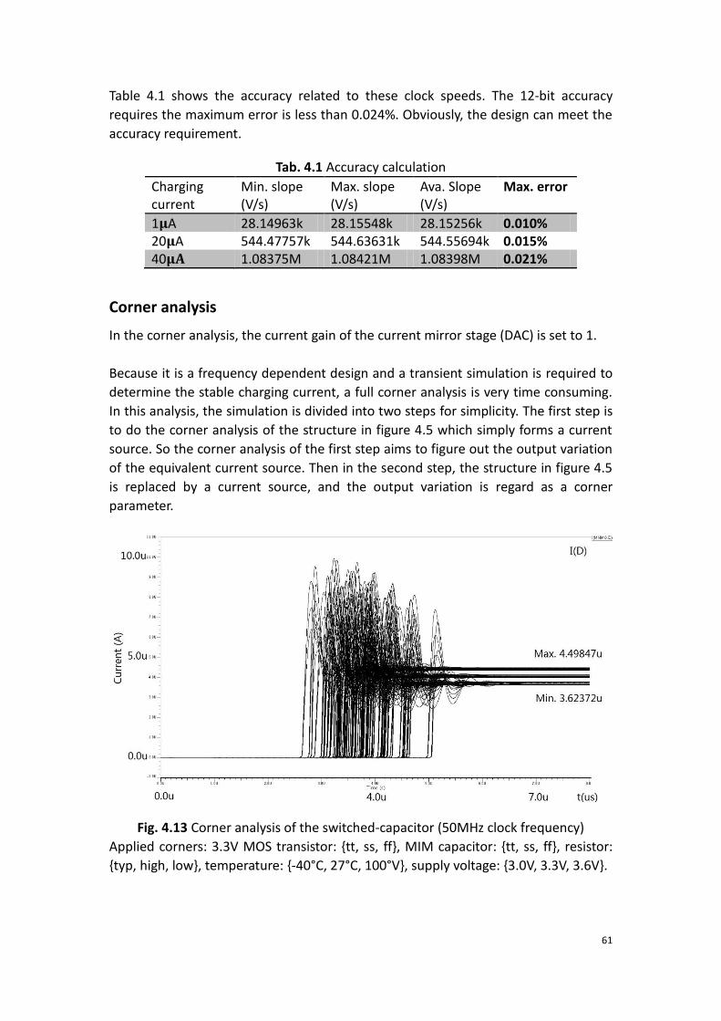
61
Table 4.1 shows the accuracy related to these clock speeds. The 12-bit accuracy
requires the maximum error is less than 0.024%. Obviously, the design can meet the
accuracy requirement.
Tab. 4.1 Accuracy calculation
Charging current
Min. slope (V/s)
Max. slope (V/s)
Ava. Slope (V/s)
Max. error
1𝛍A 28.14963k 28.15548k 28.15256k 0.010% 20𝛍A 544.47757k 544.63631k 544.55694k 0.015% 40𝛍𝐀 1.08375M 1.08421M 1.08398M 0.021%
Corner analysis
In the corner analysis, the current gain of the current mirror stage (DAC) is set to 1.
Because it is a frequency dependent design and a transient simulation is required to
determine the stable charging current, a full corner analysis is very time consuming.
In this analysis, the simulation is divided into two steps for simplicity. The first step is
to do the corner analysis of the structure in figure 4.5 which simply forms a current
source. So the corner analysis of the first step aims to figure out the output variation
of the equivalent current source. Then in the second step, the structure in figure 4.5
is replaced by a current source, and the output variation is regard as a corner
parameter.
Fig. 4.13 Corner analysis of the switched-capacitor (50MHz clock frequency)
Applied corners: 3.3V MOS transistor: {tt, ss, ff}, MIM capacitor: {tt, ss, ff}, resistor:
{typ, high, low}, temperature: {-40°C, 27°C, 100°V}, supply voltage: {3.0V, 3.3V, 3.6V}.

62
Fig. 4.14 Corner analysis of the switched-capacitor (600MHz clock frequency)
Applied corners: 3.3V MOS transistor: {tt, ss, ff}, MIM capacitor: {tt, ss, ff}, resistor:
{typ, high, low}, temperature: {-40°C, 27°C, 100°V}, supply voltage: {3.0V, 3.3V, 3.6V}.
For 50MHz clock frequency, the output current (drain current of P2 in figure 4.5)
varies from 3.624 μA to 4.498 μA. The average value is 4.061 μA. So in the second
step analysis this current variation is treated as a corner parameter to replace the
output variation of the first stage. The simulation result is shown in figure 4.15.
For 600MHz clock frequency, the output current (drain current of P2 in figure 4.5)
varies from 41.89μA to 51.63μA. The average value is 46.76μA. The second step
simulation is applied as the same method as the 50MHz case. Figure 4.16 shows the
simulation result.
Fig. 4.15 Corner analysis of the ramp generator

63
Applied corners: 3.3V MOS transistor: {tt, ss, ff}, MIM capacitor: {tt, ss, ff}, resistor:
{typ, high, low}, temperature: {-40°C, 27°C, 100°V}, supply voltage: {3.0V, 3.3V, 3.6V},
charging current: {3.624μA, 4.061μA, 4.498μA}
Fig. 4.16 Corner analysis of the ramp generator
Applied corners: 3.3V MOS transistor: {tt, ss, ff}, MIM capacitor: {tt, ss, ff}, resistor:
{typ, high, low}, temperature: {-40°C, 27°C, 100°V}, supply voltage: {3.0V, 3.3V, 3.6V},
charging current: {41.89μA, 46.76μA, 51.63μA.}
Table 4.2 shows the slope variation in the corner simulation. The typical values are
obtained under the condition of 27°C, 3.3V voltage supply and typical device models.
Tab. 4.2 Corner simulation results
Clock frequency Max. Slope (𝑽 𝝁𝒔⁄ ) Min. Slope (𝑽 𝝁𝒔⁄ ) Typ. Slope (𝑽 𝝁𝒔⁄ )
50MHz 0.138 0.092 0.112 600MHz 1.541 0.567 1.266
Power consumption corner analysis
To do the power consumption corner simulations, the switched-capacitor is replaced
by a resistor. The value of the equivalent resistor is calculated as:
𝑅𝑒𝑞𝑢𝑙 =1
𝑓×𝐶 (4-5)
As C equals to 60fF, for 50MHz clock frequency case, the switched-capacitor is
replaced by a 333.3kOhm resistor. And for 600MHz clock frequency case, the
switched-capacitor is replaced by a 27.8kOhm resistor. Table 4.2 shows a summary of
the power consumption.
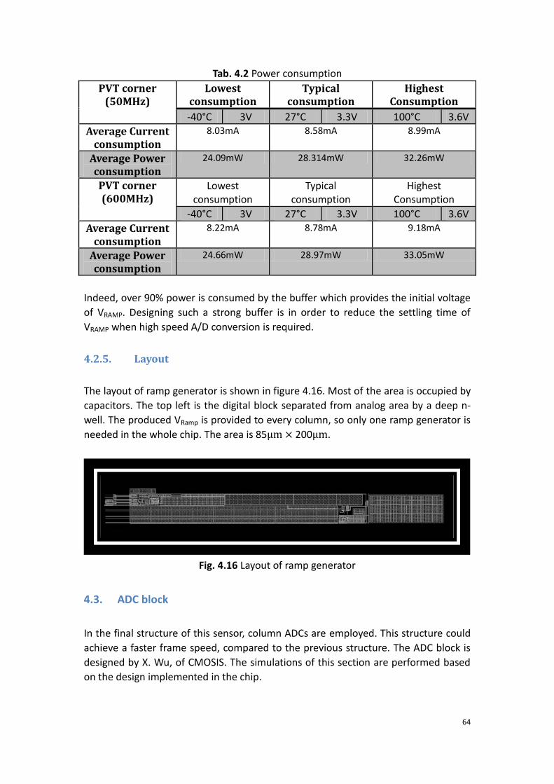
64
Tab. 4.2 Power consumption
PVT corner (50MHz)
Lowest consumption
Typical consumption
Highest Consumption
-40°C 3V 27°C 3.3V 100°C 3.6V
Average Current consumption
8.03mA 8.58mA 8.99mA
Average Power consumption
24.09mW 28.314mW 32.26mW
PVT corner (600MHz)
Lowest consumption
Typical consumption
Highest Consumption
-40°C 3V 27°C 3.3V 100°C 3.6V
Average Current consumption
8.22mA 8.78mA 9.18mA
Average Power consumption
24.66mW 28.97mW 33.05mW
Indeed, over 90% power is consumed by the buffer which provides the initial voltage
of VRAMP. Designing such a strong buffer is in order to reduce the settling time of
VRAMP when high speed A/D conversion is required.
4.2.5. Layout
The layout of ramp generator is shown in figure 4.16. Most of the area is occupied by
capacitors. The top left is the digital block separated from analog area by a deep n-
well. The produced VRamp is provided to every column, so only one ramp generator is
needed in the whole chip. The area is 85μm × 200μm.
Fig. 4.16 Layout of ramp generator
4.3. ADC block
In the final structure of this sensor, column ADCs are employed. This structure could
achieve a faster frame speed, compared to the previous structure. The ADC block is
designed by X. Wu, of CMOSIS. The simulations of this section are performed based
on the design implemented in the chip.

65
4.3.1. Principle
The comparator is an essential component in the ADC. A lot of structures have been
researched. Figure 4.17 shows the structure employed in the design.
S2
VRAMP
Comparator
out
CVSIG
VRES S1 A
Fig.4.17 Auto-zero comparator
The conversion is completed in three phases:
1. Switches S1 and S2 are turned on, and the comparator is in the unity feedback
model. The minus plain of the capacitor is short to the non-inverting input of the
comparator. The following calculation can be performed:
𝐴(𝑣𝐶 − 𝑣𝑜𝑠) = 𝑣𝐶 (4-6)
𝑣𝐶 =𝐴
𝐴+1𝑣𝑜𝑠 ≈ 𝑣𝑜𝑠 (4-7)
where, vos is the input offset of the amplifier, vC is the voltage across the
capacitor and A is the gain of amplifier.
2. Switches S1 and S2 are turned off, and the amplifier is no longer in unity feedback.
The VSIG is fed into the minus plain of the capacitor and the VRAMP (provided by
the ramp generator designed in the previous section) starts to increase. The
difference between the two input ports of the amplifier is as:
𝑣𝑑𝑖𝑓𝑓1 = 𝑣𝑆𝐼𝐺 + 𝑣𝐶 − 𝑣𝑜𝑠 − 𝑣𝑅𝐴𝑀𝑃
= 𝑣𝑆𝐼𝐺 − 𝑣𝑅𝐴𝑀𝑃 (4-8)
Hence, the offset is cancelled. If vdiff >0, the output is logical “1”; if vdiff <0, the
output is logical “0”.
3. The S1 and S2 are still open, but the VRES is fed into the minus plain of the capacitor
and the VRAMP starts to increase from the same voltage level in phase 2. The
difference between the two input ports of the amplifier is as:
𝑣𝑑𝑖𝑓𝑓2 = 𝑣𝑅𝐸𝑆 + 𝑣𝐶 − 𝑣𝑜𝑠 − 𝑣𝑅𝐴𝑀𝑃
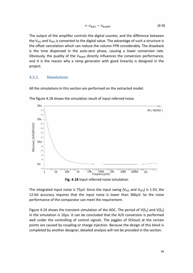
66
= 𝑣𝑅𝐸𝑆 − 𝑣𝑅𝐴𝑀𝑃 (4-9)
The output of the amplifier controls the digital counter, and the difference between
the VSIG and VRES is converted to the digital value. The advantage of such a structure is
the offset cancelation which can reduce the column FPN considerably. The drawback
is the time dispensed in the auto-zero phase, causing a lower conversion rate.
Obviously, the quality of the VRAMP directly influences the conversion performance,
and it is the reason why a ramp generator with good linearity is designed in the
project.
4.3.2. Simulations
All the simulations in this section are performed on the extracted model.
The figure 4.18 shows the simulation result of input referred noise.
Fig. 4.18 Input referred noise simulation
The integrated input noise is 75μV. Since the input swing (VSIG and VRES) is 1.5V, the
12-bit accuracy requires that the input noise is lower than 366μV. So the noise
performance of the comparator can meet the requirement.
Figure 4.19 shows the transient simulation of the ADC. The period of V(S1) and V(S2)
in the simulation is 10μs. It can be concluded that the A/D conversion is performed
well under the controlling of control signals. The joggles of V(Vout) at the certain
points are caused by coupling or charge injection. Because the design of this block is
completed by another designer, detailed analysis will not be provided in the section.

67
Fig. 4.19 Transient simulation result of ADC
4.4. Bandgap reference
The performance of analog circuits is strongly dependent on the voltage and current
references. Such references should have little dependence on power supply and
process parameters. Besides, it needs to have well-defined dependence on the
temperature under the working environment. For confidentiality agreement, this
section will not provide the actual schematic of the design, but will only show the
theoretical structure and simulation results.
4.4.1. Principle
The figure 4.11 shows the basic circuit used to produce voltage references. Since 𝑉𝐵𝐸
of a bipolar transistor has a negative temperature coefficient, generally about
-2mV/℃, a term with a positive temperature coefficient is needed to compensate it.
The voltage difference between two pn junctions, operated at different current
densities, is used to generate a proportional to absolute temperature (PTAT) current
in the resistor RPTAT (in figure 4.20). This current generates a PTAT voltage in the
resistor R2 (Since a current mirror stage is implemented, the two branches have the
same current). If the ratio between R2 and RPTAT is chosen properly, the first order
effects of the temperature dependency of the diode and the PTAT current will cancel
out.
The calculation procedure is as:
𝐼𝐶 = 𝐼𝑆 exp (𝑉𝐵𝐸
𝑘𝑇 𝑞⁄) (4-10)
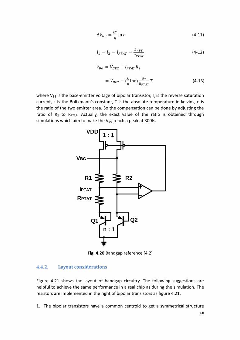
68
∆𝑉𝐵𝐸 =𝑘𝑇
𝑞ln 𝑛 (4-11)
𝐼1 = 𝐼2 = 𝐼𝑃𝑇𝐴𝑇 =∆𝑉𝐵𝐸
𝑅𝑃𝑇𝐴𝑇 (4-12)
𝑉𝐵𝐺 = 𝑉𝐵𝐸2 + 𝐼𝑃𝑇𝐴𝑇𝑅2
= 𝑉𝐵𝐸2 + (𝑘
𝑞lnr)
𝑅2
𝑅𝑃𝑇𝐴𝑇𝑇 (4-13)
where VBE is the base-emitter voltage of bipolar transistor, Is is the reverse saturation
current, k is the Boltzmann’s constant, T is the absolute temperature in kelvins, n is
the ratio of the two emitter area. So the compensation can be done by adjusting the
ratio of R2 to RPTAP. Actually, the exact value of the ratio is obtained through
simulations which aim to make the VBG reach a peak at 300K.
R1 R2
RPTAT
n : 1
Q1 Q2
VBG
1 : 1
IPTAT
VDD
Fig. 4.20 Bandgap reference [4.2]
4.4.2. Layout considerations
Figure 4.21 shows the layout of bandgap circuitry. The following suggestions are
helpful to achieve the same performance in a real chip as during the simulation. The
resistors are implemented in the right of bipolar transistors as figure 4.21.
1. The bipolar transistors have a common centroid to get a symmetrical structure

69
which can reduce the influence of linear gradient in X and Y directions.
2. The resistors (R2 and RPTAT) are laid in ABBA configuration (see in figure 4.22),
which can reduce the mismatch due to linear gradient in Y axis.
3. The input pMOS pair is laid in a cross coupled method (see in figure 4.23),
reducing the influence of linear gradient in X and Y directions.
4. The pMOS current mirror is cross coupled to improving matching.
5. Output filter composed by capacitors rounds the bandgap to increase the
distance to the sensitive nodes.
6. The bandgap is covered by metal. It is aimed to decrease the differential stress to
underlying components.
Fig. 4.21 Bandgap layout
The ABBA and across coupled configurations are referred to the layout strategies
shown in figure 4.22 and 4.23 respectively.

70
Y D
ire
cti
on
A
B
B
A
A
B
B
A
B
A
A
BY D
ire
cti
on
X Direction
Fig. 4.22 ABBA configuration Fig. 4.23 Across coupled configuration
4.4.3. Simulation results
All the simulations in this section are performed on the extracted models.
Figure 4.24 shows the transient startup behavior. All process variations have been
taken into account, including a temperature range of -40°C to 100°V and a supply
voltage of 3.0V to 3.6V. As can be seen from the figure, the maximum startup time is
approximately 50μs .
The output voltage at 60μs is displayed in figure 4.25, where it is plotted against the
supply voltage. The bandgap voltage is between 1.163 and 1.234, yielding a 5.9%
spread over PVT (process, voltage and temperature).
The output voltage versus temperature characteristic is shown in figure 4.26. The
ratio of the resistors and BJT’s are chosen in such a way that the maximum voltage is
centered at 27°C.
In figure 4.27, the power supply rejection ratio (PSRR) simulation result is shown. It
can be seen that the disturbances on the supply line are attenuated by more than
58dB.

71
Fig. 4.24 Transient startup behavior. Applied corners: 3.3V MOS transistor:
{tt, ss, ff, fs, sf}, bipolar transistor: {tt, ss, ff}, resistor: {typ, high, low},
temperature: {-40°C, 27°C, 100°V}, supply voltage: {3.0V, 3.3V, 3.6V}.
Fig. 4.25 Output voltage at 60μs. Applied corners: 3.3V MOS transistor: {tt,
ss, ff, fs, sf}, bipolar transistor: {tt, ss, ff}, resistor: {typ, high, low},
temperature:{-40°C, 27°C, 100°V}. Supply voltage {3.0 to 3.6 increased by
0.1}.

72
Fig. 4.26 Temperature dependence of bandgap voltage
Fig. 4.27 Power supply rejection ratio, typical case
4.4.4. Summary
Table 4.3 lists the specifications of the designed bandgap circuit.
Table 4.3 Bandgap circuit specifications
Content Value Unit
Supply voltage 3.3 [V] Output voltage 1.19 [V] Temperature range [-40, 100] [°C]

73
Nominal current consumption 39.6 [μA] PVT accuracy 5.9 [%] Power supply rejection ratio >58 [dB] Area 275 × 160 [μm × μm]
4.5. Biasing circuit
In analog circuits, biasing blocks are needed to provide accurate biasing voltages and
currents for amplifiers, column loads, ramp generator, etc. The whole biasing block is
relatively complex in this HDR image sensor chip. For simplicity, only a few important
components in the design will be given in the section. There are a 6-bit digital to
analog convertor (DAC) and a rail-to-rail amplifier.
4.5.1. 6-bit digital to analog convertor
Principle
In this chip, a 6-bit adjustable voltage biasing block is designed. The DAC conversion
concept is shown in figure 4.28. There are six pairs of B and B̅ input signals. The
labels in the left part are defined by Cadence. It can be studied by an example:
<*4>((<*8>BB<5>), (<*8>B<5>)). It means the 1 to 8, 17 to 24, 33 to 40 and 49 to 56
ports are connected to BB; the 9 to 16, 25 to 32, 41 to 48 and 57 to 64 ports are
connected to B.
X64
1:64
1
2
64
<*1>((<*32>BB<5>),(<*32>B<5>))
VLOW
VHIGH
VDAC
<*2>((<*16>BB<5>),(<*16>B<5>))
<*4>((<*8>BB<5>),(<*8>B<5>))
<*8>((<*4>BB<5>),(<*4>B<5>))
<*16>((<*2>BB<5>),(<*2>B<5>))
<*32>((<*1>BB<5>),(<*1>B<5>))
3
Fig. 4.28 Digital to analog convertor
The left part in figure 4.28 determines the states of the switches in the right part.
According to the input signals, one and only one switch is turned on and others are
turned off at certain moment. Hence, the output voltage varies from 𝑉𝐿𝑂𝑊
to 𝑉𝐿𝑂𝑊 +63(𝑉𝐻𝐼𝐺𝐻−𝑉𝐿𝑂𝑊)
64.

74
Simulation results
The simulation is performed on the extracted model
Figure 4.29 shows that the outputs of the DAC varies from 1.2V (VLOW) to 2.68V
(highest output voltage) step by step, according to the increase of digital input value
(from 000000 to 111111). The result illustrates that the simulation results match the
calculation values very well.
Fig. 4.29 DAC outputs
In fact, the VLOW can be as low as VGND and VHIGH can as high as 3.3V in this design.
The output range can be chosen based on practical requirements.
4.5.2. Rail-to-rail buffer
Behind the DAC, a rail-to-rail buffer is needed to enhance the driving strength of the
related components. As mentioned in the former section, the designed DAC’s output
voltage has a range from 0V to 3.3V. In this application, both the input and output of
the buffer need to vary from 0.6V to 2.7V, so a single nMOS or pMOS input pair
cannot meet the requirement. The estimated load capacitance is as large as 20pF.
Figure 4.30 shows the schematic of the buffer.

75
OUT
VDD
VSS
CMDN
INP INN INN INP
Fig. 4.30 Rail-to-rail buffer
Simulation results
The simulation is performed on the extracted model
The closed loop AC response and transient simulation results are shown in figure
4.31 and 4.32 respectively. The load is a 20pF capacitor. The AC simulation result
illustrates the bandwidth of this buffer is 235MHz and no peak exists in the gain
versus frequency curve. The transient simulation result shows the maximum working
speed is over 10MHz (because this block is used to set DC values, 10MHz is fast
enough) with a swing larger than 0.6V to 2.7V. The power consumption is 10mW.
Fig. 4.31 AC response of the buffer

76
Fig. 4.32 Transient simulation result
In fact, in the voltage biasing block, several rail-to-rail buffers with a similar structure
are designed according to the requirements of the driving strength.
4.5.3. Layout
Figure 4.33 and 4.34 are the layout of the voltage and current biasing blocks
respectively. The voltage biasing block has dimensions of 1800μm ×85μm and the
current biasing block costs 1100μm × 85μm area.
Fig. 4.33 Layout of voltage biasing
Fig. 4.34 Layout of current biasing
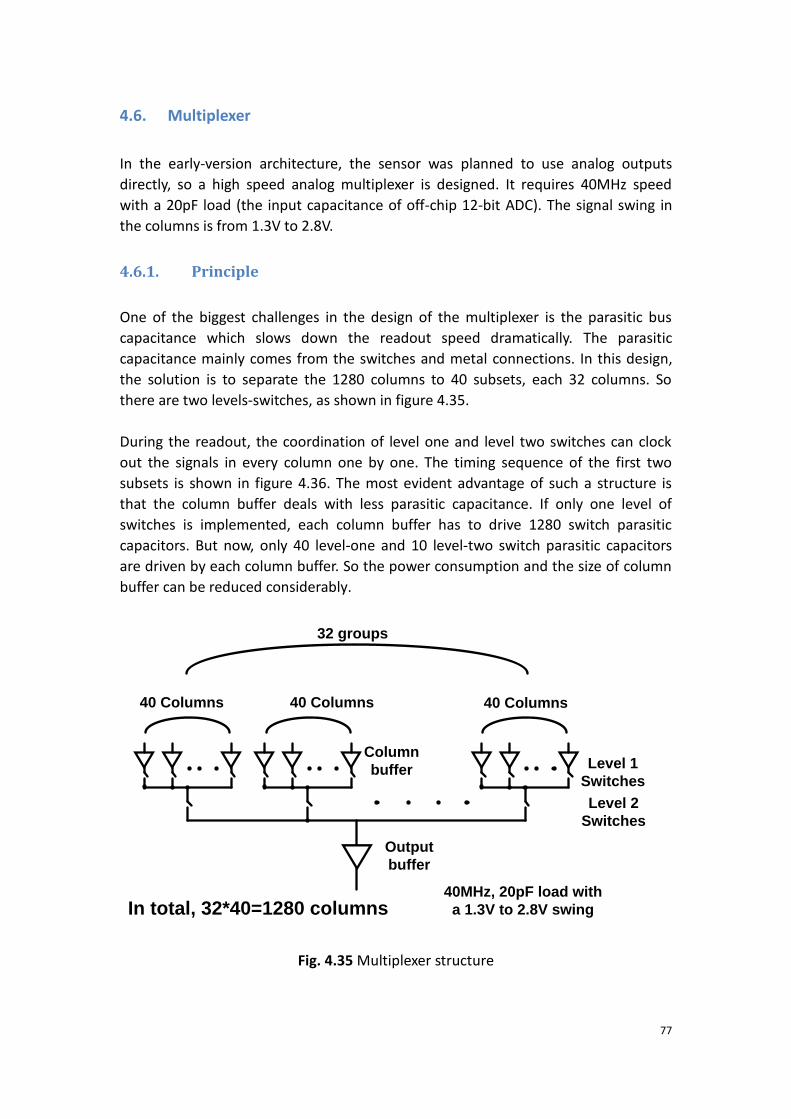
77
4.6. Multiplexer
In the early-version architecture, the sensor was planned to use analog outputs
directly, so a high speed analog multiplexer is designed. It requires 40MHz speed
with a 20pF load (the input capacitance of off-chip 12-bit ADC). The signal swing in
the columns is from 1.3V to 2.8V.
4.6.1. Principle
One of the biggest challenges in the design of the multiplexer is the parasitic bus
capacitance which slows down the readout speed dramatically. The parasitic
capacitance mainly comes from the switches and metal connections. In this design,
the solution is to separate the 1280 columns to 40 subsets, each 32 columns. So
there are two levels-switches, as shown in figure 4.35.
During the readout, the coordination of level one and level two switches can clock
out the signals in every column one by one. The timing sequence of the first two
subsets is shown in figure 4.36. The most evident advantage of such a structure is
that the column buffer deals with less parasitic capacitance. If only one level of
switches is implemented, each column buffer has to drive 1280 switch parasitic
capacitors. But now, only 40 level-one and 10 level-two switch parasitic capacitors
are driven by each column buffer. So the power consumption and the size of column
buffer can be reduced considerably.
40 Columns
32 groups
Level 1
Switches
Level 2
Switches
Output
buffer
Column
buffer
In total, 32*40=1280 columns40MHz, 20pF load with
a 1.3V to 2.8V swing
40 Columns 40 Columns
Fig. 4.35 Multiplexer structure

78
SS1
SS2
S1
S2
S32
S33
S34
S64
Fig. 4.36 Timing sequence of switches
SS1 and SS2 represent the level-two switches, and S1, S2, S3 etc. are the level-one
switches.
The output stage of the multiplexer is a rail-to-rail buffer which can drive a 20pF
capacitive load at 40MHz rate.
4.6.2. Sequence generation block
This block is producing control signals for the level-one and the level-two switches
based on a shift-register structure. Only three outside control signals, Read, Reset
and Clock, are required.
Read
Reset
Clock
VDD VGND SW_Level_1<1:1280>
SW_Level_2<1:32>
Col_Bus_Enable<1:1280>
Shift_Out
Fig. 4.37 Sequential generator block
First of all, the reset signal is fed in to clear all the D flip-flops (reset to a low voltage

79
level). Afterwards, a “Read” command which has a pulse width of 25ns (related to
40MHz working speed) is sent to the block. Then the sequential circuit starts to work
cooperating with of the clock signal (40MHz).
In the design, the column buffer owns an “Enable” port to control the states (working
or sleeping) of the buffer. The enable signal of the column buffer is provided by a
clock period before the column buffer starts to export a signal. It is because a setup
time is needed to make sure the buffer operates correctly. So in any moment, only
two column buffers are active: one is working and the other is in the stand-by state.
Through this method, a higher readout speed can be achieved at the cost of double
energy consumption. The “SW_Level-1” signals are produced by shifting the “Read”
pulse in D flip-flops. The “SW_Level-2” signals are obtained by Boolean calculation.
The “Shift_Out” port is used to clock out the data in D flip-flop chain for testability.
4.6.3. Simulation results
The simulations are performed on the schematic model. Due to the architecture
change, the layout is cancelled.
Because of the complexity of the complete multiplexer, only 120 columns are
simulated to verify the performance. Similar to the actual multiplexer, 40 columns
form a subset. So in total, 3 subsets are simulated. Besides, the metal parasitic
capacitance is taken into account during the simulation. Figure 4.38 shows the test
signals distributed to the first subset, column 1 to 40. The other two subsets have the
same test signals as the graph shown. Such a test bench can be used to check the
settling performance of the multiplexer in the conditions of low-to-low, low-to-high,
high-to-high, high-to-low and normal variations. Figure 4.39 shows the results of the
sequential generator. The results match the design perfectly and the multiplexer
works correctly under the control of the sequential block.
Fig.4.38 Test signals
1,3 1,4
1,5 1,6
1,7 1,8
1,9 2
2,1 2,2
2,3 2,4
2,5 2,6
2,7 2,8
2,7 2,6
2,5 2,4
2,3 2,2
2,1 2
1,9 1,8
1,7 1,6
1,5 1,4
1,3 1,3 1,4
1,3
2,8 2,7
2,8 2,8
1,3
2,8
1 3 5 7 9 11 13 15 17 19 21 23 25 27 29 31 33 35 37 39

80
Fig. 4.39 Simulation of the sequence generation block (The vertical axes shown above
represent the voltage range from 0 V to 3.3 V for every waveform)
Fig. 4.40 Transient simulation result with the test signals shown in figure 4.38

81
Fig. 4.41 The zoom-in figure of the output
Figure 4.40 shows the transient simulation result of 120 columns. The multiplexer
clocks out the data of 120 columns sequentially. Figure 4.41 is the zoom-in graph of
the multiplexer output. Firstly, since the output mismatch between columns at the
same input voltage is lower than 0.02‰, the settling behavior can meet the 12-bit
accuracy requirement (the settling accuracy is better than the accuracy of the off-
chip ADC). Secondly, the settling time of the capacitive load is less than 25ns (40MHz
working speed). The power consumption is around 165mW.
4.7. Noise calculation
The noise performance of the readout circuitry is important and directly influences
the SNR. In this section, a detailed calculation of the system noise is given. Figure
4.42 shows the column analog chain in the design. Before calculation, a noise model
is provided. The main noise sources include the source follower noise, the PGA input
referred noise, the comparator input referred noise and the ADC quantization noise.
The noise model is built as shown in figure 4.43. VNoise,SF stands for the source
follower input-referred noise, VNoise,PGA is the PGA input-referred noise, VNoise, Comp is
the ADC input-referred noise and VNoise, Quantizaion is the ADC quantization noise. SF and
RS represent the source follower and row select switch respectively. Cbus is the
column bus parasitic capacitance and CH is the sampling capacitor.
The ADC quantization noise is:
𝑉𝑛𝑜𝑖𝑠𝑒 =𝑓𝑢𝑙𝑙−𝑠𝑐𝑎𝑙𝑒
2𝑁√12 (4-14)
Here, N=12 and full-scale equals to 1.5V. The other values of noise are obtained from

82
simulations.
RSPGA
S&H ADC
RampCbus CH
SF
Column
bias
Fig. 4.42 Analog readout chain
RSPGA
S&HADC
RampCbus CH
SFVNoise,SF
VNoise,
PGA
VNoise,
Comp
VNoise,
Quantization
Gain=0.86
Gain=1.12(low gain)Gain=3.40(high gain)
Column
bias
Fig. 4.43 Noise model
Since all the noise sources are not correlated, the total noise can be calculated as:
(𝑉𝑁𝑜𝑖𝑠𝑒,𝑡𝑜𝑙)𝑅𝑀𝑆 = √𝑉𝑁𝑜𝑖𝑠𝑒,12 + 𝑉𝑁𝑜𝑖𝑠𝑒,2
2 + 𝑉𝑁𝑜𝑖𝑠𝑒,32 + ⋯ (4-15)
It is necessary to point out that a scaled conversion is performed when the noise is
transferred across a gain stage. Besides, the reset noise (kT/C noise) of the floating
diffusion is cancelled by correlated double sampling technology.
Table 4.4 shows the details of noise sources
Tab. 4.4 Noise value of each block
Noise Unit Low gain channel High gain channel
Conversion gain μV/𝑒− 29.73 103.89 SF input-referred noise μV 320.0 320.0 PGA input -referred noise μV 120.2 40.3 ADC input -referred noise μV 75.1 75.1 A/D quantization noise μV 105.7 105.7 Equivalent source follower input -referred noise
μV 374.15 326.44
Equivalent pixel noise 𝑒− 12.6 3.1

83
Clearly, for both channels, the source follower is the dominant noise source.
Especially for the high conversion gain channel, the source follower contributes over
98% noise to the total equivalent input-referred noise. Since the PGA stage provides
a gain of (×3.40), the noise behind the PGA stage is considerably compressed. For
the low conversion gain channel, the PGA only provides a gain of (×1.12), so the
compression of the noise is limited. In summary, the designed sensor achieves an
input-referred noise as low as 3.1𝑒−.
4.8. Frame speed calculation
The frame speed is a significant specification of CMOS image sensor. Figure 4.44
shows the data flow in the readout process. In this design, since the readout process
employs a pipelined structure, the speed is limited by the slowest block. The frame
rate can be calculated by the following equation:
𝑇𝐹𝑟𝑎𝑚𝑒 = 𝑇𝐹𝑂𝑇 + 𝑇𝑙𝑖𝑛𝑒 𝑡𝑖𝑚𝑒 × 𝑁𝑟. 𝑅𝑜𝑤 (4-17)
where the TFrame presents the time consumed in taking one frame, Tline time is the line
time used to obtain one row signals. The Tline time is determined by the block
consuming the longest time. TFOT (Frame Overhead Time) can be treated as the
overhead time of each frame. Nr.Row is the number of rows in the sensor.
AFEA/D
conversion
LVDS
Output
Fig. 4.44 Pipelined output structure
In this design, the time consumed in the Analog-Front-End (AFE) is around 5μs. The
value is obtained by estimation. Indeed, by adjusting the column current source and
the PGA biasing current, the time consumed in AFE can be varied.
The A/D conversion time of the designed ramp ADC depends on the clock frequency
of the counters and the conversion accuracy. Assuming the counters work at 400MHz
frequency, the time TA/D required to complete one full 12-bit A/D conversion process
is:
𝑇𝐴/𝐷 =1
400𝑀𝐻𝑧× 4096 = 10.24μs
As mentioned above, due to the double sampling technology, two A/D conversions
are required to obtain an effective signal. However, because the reset level is
basically known, only a part of ramp voltage is needed. Therefore, a relative short
time is required to finish the A/D conversion in the phase of measuring the reset

84
level. Assuming 25% TA/D is distributed to the partly A/D conversion process and
waiting time. The total time TA/D,total distributed in the ADC block is:
𝑇𝐴 𝐷⁄ ,𝑡𝑜𝑡𝑎𝑙 = (100% + 25%) × 𝑇𝐴 𝐷⁄ = 12.8𝜇𝑠
In the design, both the top and bottom sides have 12 channel LVDS output drivers. So
the data (12-bit data due to 12-bit ADC) of one column can be exported in one clock
period. Since the chip has 1280 columns, if a 120MHz clock is applied to the drivers,
the time TLVDS required to output a row data is:
𝑇𝐿𝑉𝐷𝑆 =1
120𝑀𝐻𝑧× 1280 = 10.7𝜇𝑠
Since the A/D conversion process consumes the longest time, the Tline time equals to
TA/D, total due to the implemented pipeline structure. In the design, compared to the
latter item in the formula (4-17), the TFOT can be ignored, because it is far less than
the time consumed in reading the data of 1024 rows. The frame speed is about 76fps
(the sensor has 1024 rows).
4.9. Summary
The analog readout circuits are implemented at both sides of the sensor array. One
side is dedicated for the high gain channel and the other one is used for the low gain
channel. The equivalent input-referred noise is as low as 3.1𝑒−, the frame speed can
reach 76fps at 400MHz ADC clock.
4.10. Reference
[4.1] X.Ge “The design of globe shutter CMOS image sensor in 110nm technology”
Master thesis, Delft University of Technology, 2012.
[4.2] Willy M. C. Sansen “Analog Design Essentials”, Chapter 16 “Bandgap and
current reference circuits”, page 325, ISBN 9787302163404.

85
Chapter 5 Conclusions and future work
5.1. Conclusions
In this thesis, a dual-transfer-gate high-dynamic-range CMOS image sensor is
designed in 110nm technology. The sensor contains 1280 columns and 1024 rows
with 4.8μm pixel pitch. The sensor is targeted to have a dynamic range up to 84.5dB
and an input-referred noise level as low as 3.1𝑒−. This result is achieved by applying
a column-level ADC structure. The frame speed is around 76fps with 12-bit digital
output format.
By introducing a second FD node, a high FWC in combination with high conversion
gain, thus low input-referred noise, can be achieved at the same time. For high
illumination conditions, the low gain channel provides effective output signals. On
the contrary, for darker objects, the high gain channel can be chosen, which can
compress the noise and provides clearer output signals. The final image is obtained
by restructuring the information taken from the two channels. The SNR dip at the
transition between the two different gain channels is as low as 0.13dB.
The analog readout circuitry is designed at both sides of the sensor array. One side is
dedicated for the high gain channel and the other one is used for the low gain
channel. The voltage reference of the chip is obtained from the bandgap reference
block which yields a 5.9% spread over PVT (process, voltage and temperature) and
has a 58dB PSRR (power supply rejection ratio). The column ramp ADC, whose
reference voltage is provided by an auto-scaling ramp generator, is implemented on
the sensor chip to speed up the reading process. The designed ADC has a 12-bit
conversion accuracy. Through programming of the built-in registers, the biasing
blocks could produce the desired biasing voltage and current signals. 24 LVDS output
drivers are employed on the chip to speed up the reading rate. Besides, the analog
multiplexer could achieve a readout speed of more than 40MHz.
5.2. Future work
By the time of writing this thesis, the layout and post-simulation of all functional
blocks have been finished, but still the top-level design, simulation and verification
needed to be carried out.
The goal of the thesis was to design a high dynamic range image sensor. In this
sensor, the dynamic range is limited by the area of the photodiode, conversion gain

86
and source follower noise. Hence, generally, the HDR performance can be enhanced
through three aspects. First, increasing the FWC through fabrication process
optimization; the second is to increase the conversion gain to further reduce the
input-referred noise; the third is to decrease the source follower noise. All above
mentioned possible improvement requires processing optimization, characterization
and design iterations.
In order to verify the sensor specifications under different process and operation
condition, more simulations are required to check the performance of every block.
Besides, because of inadequate processing simulation files, Monte Carlo simulations
could not be performed in the design phase. In addition, for the auto-scaling ramp
generator, completed frequency-dependent simulations should be performed to
obtain a detailed quality of ramp voltage in the whole working range.