The 6809 Part 1: Design Philosophy - Retro · The 6809 Part 1: Design Philosophy Terry Ritter Joel...
29
The 6809 Part 1: Design Philosophy Terry Ritter Joel Boney Motorola, Inc. 3501 Ed Blustein Blvd. Austin, TX 78721 This is a story. It is a story of computers in general, specifically microcomputers, and of one particular microprocessor - with revolutionary social change lurking in the background. The story could well be imaginary, but it happens to be true. In this 3 part series we will describer the design of what we feel is the best 8 bit machine so far made by human: the Motorola M6809. Philosophy A new day is breaking; after a long slow twi- light of design the sun is beginning to rise on the microprocessor revolution. For the first time we have mass production computers; expensive cus- tom, cottage industry designs take on less impor- tance. Microprocessors are real computers. The first and second generation devices are not very sophisticated as processors go, but the are general- purpose logic machines. Any microprocessor can eventually be made to solve the same problems as any large scale computer, although this may be an easier or harder task depending on the micro- processor. (Naturally, some jobs require doing processing fast, in real time. We are not discussing those right now. We are discussing getting a big job done sometime.) What differentiates the class- es is a hierarchy of technology, size performance, and curiously, philosophy of use. A processor of given capability has a fixed general complexity in terms of digital logic ele- ments. Consider the computers that were built using the first solid state technology. In short they consisted of many thousands of individual transis- tors and other parts on hundreds of different print- ed circuit boards using thousands of connections and miles of connecting wire. A big computer was a big project and a very big expense. This simple economic fact fossilized a whole generation of technology into the “big computer philosophy.” Because the big computer was so expensive, time on the computer was regarded as a limited and therefore valuable resource. Certainly the time was valuable to researchers who could now look more deeply into their equations than ever before. Computer time was valuable to business people who became at least marginally capable of analyz- ing the performance of an unwieldy bureaucratic organization. And the computer makers clearly thought that processor time was valuable too; or was a severely limited resource, worth as much as the market would bear. Processor time was a limited resource. But some of us, a few small groups of technologists, are about to change that situation. And we hope we will also change how people look at computers, and how professionals see them too. Computer time should be cheap; people time is 70 years and counting down. The large computer, being a very expensive resource, quickly justified the capital required to investigate optimum use of that resource. Among the principal results of these projects was the development of batch mode multiprocessing. The computer itself would save up the various tasks it had to do, then change from one to the other at computer speeds. This minimized the wasted time between jobs and spawned the concept of an oper- ating system. Photo 1: Systems architects Ritter (right) and Boney review some of the 6809 design documents. This work results in a complete description of the desired part in a 200 page design specification. The specification is then used by logic designers to develop flowcharts of internal operations on a cycle by cycle basis.
Transcript of The 6809 Part 1: Design Philosophy - Retro · The 6809 Part 1: Design Philosophy Terry Ritter Joel...
The 6809Part 1: Design Philosophy
Terry RitterJoel BoneyMotorola, Inc.3501 Ed Blustein Blvd.Austin, TX 78721
This is a story. It is a story of computers ingeneral, specifically microcomputers, and of oneparticular microprocessor - with revolutionarysocial change lurking in the background. The storycould well be imaginary, but it happens to be true.In this 3 part series we will describer the design ofwhat we feel is the best 8 bit machine so far madeby human: the Motorola M6809.
Philosophy
A new day is breaking; after a long slow twi-light of design the sun is beginning to rise on themicroprocessor revolution. For the first time wehave mass production computers; expensive cus-tom, cottage industry designs take on less impor-tance.
Microprocessors are real computers. Thefirst and second generation devices are not verysophisticated as processors go, but the are general-purpose logic machines. Any microprocessor caneventually be made to solve the same problems asany large scale computer, although this may be aneasier or harder task depending on the micro-processor. (Naturally, some jobs require doingprocessing fast, in real time. We are not discussingthose right now. We are discussing getting a bigjob done sometime.) What differentiates the class-es is a hierarchy of technology, size performance,and curiously, philosophy of use.
A processor of given capability has a fixedgeneral complexity in terms of digital logic ele-ments. Consider the computers that were builtusing the first solid state technology. In short theyconsisted of many thousands of individual transis-tors and other parts on hundreds of different print-ed circuit boards using thousands of connectionsand miles of connecting wire. A big computer wasa big project and a very big expense. This simpleeconomic fact fossilized a whole generation oftechnology into the “big computer philosophy.”
Because the big computer was so expensive,time on the computer was regarded as a limitedand therefore valuable resource. Certainly the timewas valuable to researchers who could now lookmore deeply into their equations than ever before.Computer time was valuable to business peoplewho became at least marginally capable of analyz-
ing the performance of an unwieldy bureaucraticorganization. And the computer makers clearlythought that processor time was valuable too; orwas a severely limited resource, worth as much asthe market would bear.
Processor time was a limited resource. Butsome of us, a few small groups of technologists,are about to change that situation. And we hope wewill also change how people look at computers,and how professionals see them too. Computertime should be cheap; people time is 70 years andcounting down.
The large computer, being a very expensiveresource, quickly justified the capital required toinvestigate optimum use of that resource. Amongthe principal results of these projects was thedevelopment of batch mode multiprocessing. Thecomputer itself would save up the various tasks ithad to do, then change from one to the other atcomputer speeds. This minimized the wasted timebetween jobs and spawned the concept of an oper-ating system.
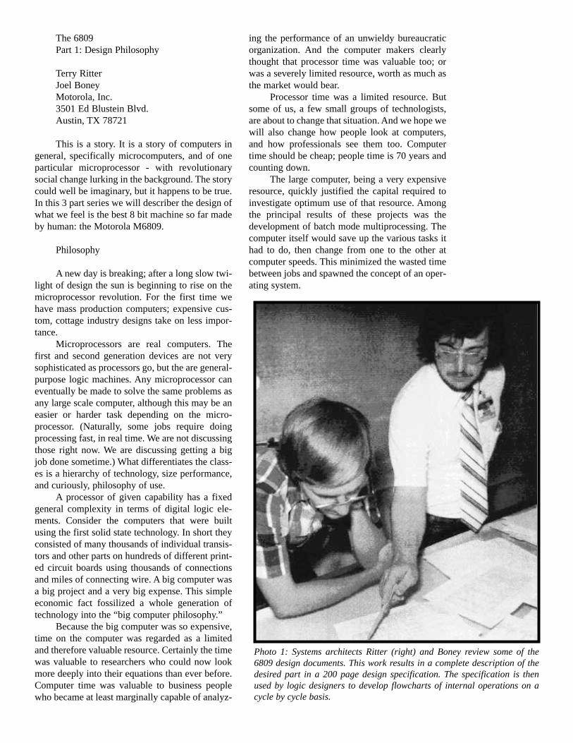
Photo 1: Systems architects Ritter (right) and Boney review some of the6809 design documents. This work results in a complete description of thedesired part in a 200 page design specification. The specification is thenused by logic designers to develop flowcharts of internal operations on acycle by cycle basis.
People were in the position of waiting forthe computer, not because they were less impor-tant than the machine, but precisely because it wasa limited resource (the problems it solved werenot).
Electronics know-how continued to develop,producing second generation solid state technolo-gy: families of digital logic integrated circuitsreplaces discrete transistors designs. This newtechnology was exploited in two main thrusts: bigcomputers could be made conceptually bigger (orfaster, or better) for the same expense, or comput-ers could be made physically smaller and lessexpensive. These new, smaller computers (mini-computers) filled market segments which couldafford a sizable but not huge investment in both
equipment and expertise. But most people, includ-ing scientists and engineers, still used only thevery large central machines. Rarely were mini-computers placed in schools; few computer sci-ence or electrical engineering departments (whomight have been at the leading edge of new gener-ation technology) used them for general instruc-tion.
And so the semiconductor technologistsbegan a third generation technology: the ability tobuild a complete computer on a single chip of sil-icon. The question then became, “How do we usethis new technology (to make money)?”
The semiconductor producer’s problem withthird generation technology wa that an unbeliev-ably large development expense was (and is)required to produce just one large scale integration(LSI) chip. The best road to profit was unclear; fora while, customer interconnection of gate arrayintegrated circuits was tried, then dropped.Complete custom designs were (and are) found tobe profitable only in vary large volumes.
Another road to profit was to produce a fewprogrammable large scale integration deviceswhich could satisfy the market needs (in terms oflarge quantities of different systems) and the fac-tory;s needs (in terms of volume production ofexactly the dame device). Naturally, the general-purpose computer was seen as a possible answer.
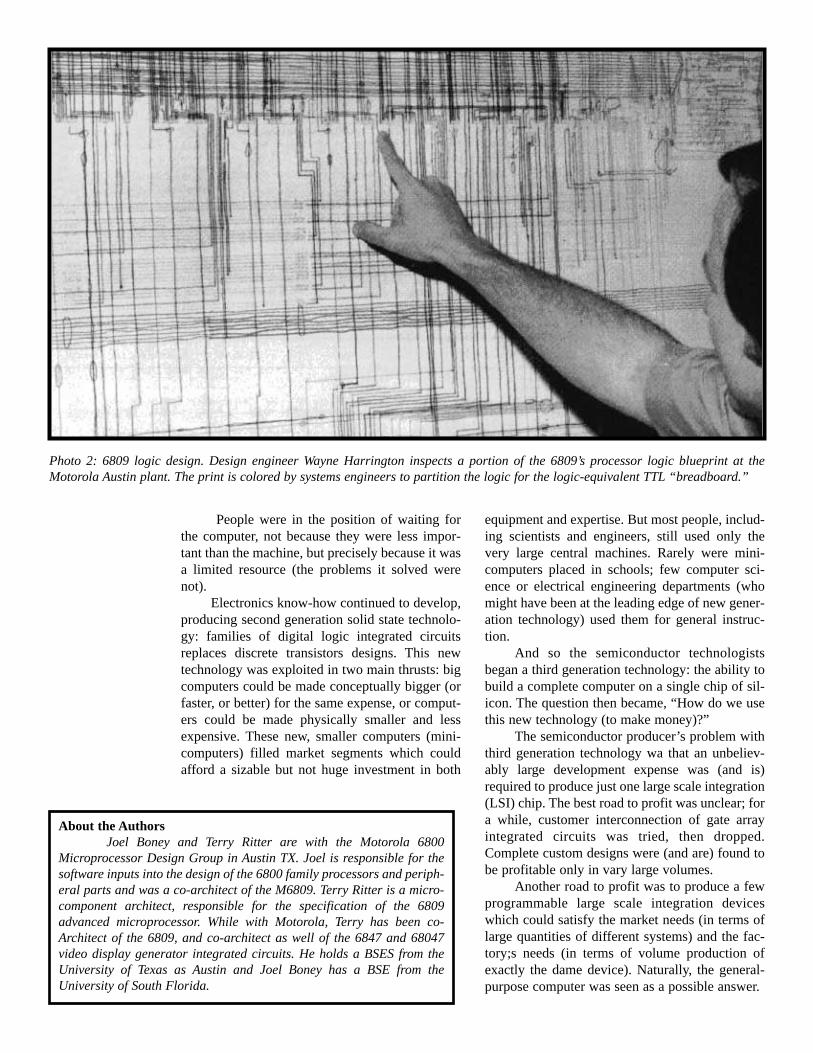
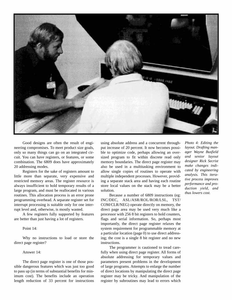
Photo 2: 6809 logic design. Design engineer Wayne Harrington inspects a portion of the 6809’s processor logic blueprint at theMotorola Austin plant. The print is colored by systems engineers to partition the logic for the logic-equivalent TTL“br eadboard.”
About the AuthorsJoel Boney and Terry Ritter are with the Motorola 6800
Microprocessor Design Group in Austin TX. Joel is responsible for thesoftware inputs into the design of the 6800 family processors and periph-eral parts and was a co-architect of the M6809. Terry Ritter is a micro-component architect, responsible for the specification of the 6809advanced microprocessor. While with Motorola, Terry has been co-Architect of the 6809, and co-architect as well of the 6847 and 68047video display generator integrated circuits. He holds a BSES from theUniversity of Texas as Austin and Joel Boney has a BSE from theUniversity of South Florida.
So what was the market for a general-pur-pose computer? The first thought was to enter theold second generation markets; ie: replacement ofthe complex logic of small or medium scale inte-gration. Control systems, instruments and specialdesigns could all use a simular processor, but thisdesigner was the key. Designers (or design man-agers)had to be converted from their heavy firstand second generation logic design backgroundsto the new third generation technology. In sodoing, some early marketing strategists over-looked the principal microprocessor markets.
Random logic replacement was by no meansa quick and sufficient market for microprocessors.In particular, the design cycle was quite long,users we often unsophisticated in their use of com-puters, and the unit volumes was somewhat small.Only when microprocessors entered high volumemarkets (hobby, games, etc) did the manufacturesbegin to make money and thus provide a crediblereason (and funds) for designing future micro-processors. Naturally, the users who wanted morefeatures were surprised that it was taking so longto get new designs - they knew what was needed.
Thus semiconductor makers began to realizethat their market was more oriented to hobbyapplications that to logic replacement, and wasmore generalized than they had thought. But eventhe hobby market was saturable.
Meanwhile companies continued to improveproduction and reduce costs, and competitiondrove process down into the ground. Where couldthey sell enough computers for real volume pro-duction, the wondered. One answer was the per-sonal computer!
Design of Large Scale Integration Parts
The design of a complex large scale integra-tion (LSI) part may be conveniently broken intothee phases: the architectural design, the logic andthe layout software and hardware (breadboard)simulations. Each phase ha its own requirements.
The architect/systems designers represent theuse of the device, the need of the marketplace andthe future needs of all customers. They proposewhat a specific customer should have that couldalso be used by other customers, possible in dif-ferent ways. They advocate what the customerswill really want, even when if no customers can beidentified who know that they will want it. that itis possible or that they will want it. The attitudethat “I know what is best for you” and be irritatingto most people, but it is necessary in order to makemaximum use of a limited resource (in this case, asingle LSI design). The architect eventually gener-ates the design specification used in subsequent
phases of the design.Logic design consists of the production of a
cycle by cycle flowchart and the derivation of theequations and logic circuitry necessary to imple-ment the specified design. This is a job ofimmense complexity and detail, but it is absolute-ly crucial to the entire project. Throughout thisphase, the specification may be iterated toward alocal optimum of maximum features at minimumlogic (and thus cost). The architectural design con-tinues, and techniques are developed to cross-check on the logical correctness of the architec-ture.
The third phase is the most hectic in terms ofdemands and involvement. By this time, manypeople know what the product is and see theresulting part merely as the turning of an imple-mentation “crank.” It seems to those who are notinvolved in this phase that more effort could casethat crank to turn faster. Since the product could besold immediately, delay is seen as a real loss ofincome. In actual practice, more effort will some-times “break the crank.”
A medium scale integration logic implemen-tation (usually transistor-transistor logic, forspeed) is required to verify the logic design. Aprocessor emulation may require ten differentboards of 80 medium scale integrated circuits eachand hundreds of board to board interconnections.Each board will likely require separate testing, andonly then will the emulation represent the proces-sor to come. Extensive test programs are requiredto check out each facet of the part, each instruc-tion, and each addressing mode. This testing may
The other major deviceneeded for home com-puters–the video displaygenerator color TVinterface–is presently involume production.Several versions areavailable, many derivedfrom the originalMotorola architecture
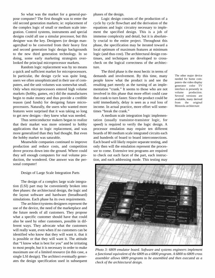
Photo 3: 6809 emulator board. Software and systems engineers implementa functional equivalent of the 6809 as a 6800 program. A 6800 to 6809 crossassembler allows 6809 programs to be assembled and then executed as acheck of the architectural design.
detect logic design errors that will have to be fixedat all levels of design.
Circuit design, in the context of the semicon-ductor industry, depends upon running computersimulation (which require sophisticated devicemodels) of signals at various nodes to verify thatthey will meet the necessary speed requirement.Transistors are sized and polysilicon lines changedto provide reliable worst case operation.
Layout is the actual task of arranging transis-tors and interconnections to implement the logicdiagram. Circuit design results will indicate appro-priate transistor sizes and polysilicon widths; thesemust now be arranged for minimum area. Everyattempt is made to make general logic “cells”which can be used in many places across the inte-grated circuit, but minimization is the principalconcern.
The layout for the chip eventually exists onlyas a computer data base. Each cell is individuallydigitized into the computer, where is can be arbi-trarily positioned, modified or replicated asdesired. Large 2 by 3 m (6.5 by 10 feet) plots of
various areas of the chip arehand checked to the logicdiagram by layout and cir-cuit designers as finalchecks of the implementedcircuit.
When layout is com-plete, the computer data
base that represents the chip design is sent to themask shop (the mask is a photographic stencil ofthe part used in the manufacturing process). At themask shop precision plotting and photographicstep and repeat techniques are used to produceglass plates for each mask layer. Each mask coversan entire wafer with etched nickel or chrome lay-outs at real chip size. (Atypical LSI device will bebetween 5 by 5 and 7.6 by 7.4 mm (0.2 by 0.2 and0.3 by 0.3 inches). These masks are used to exposephotosensitive etch resist the will protect someareas of the wafer from the chemical processeswhich selectively add the impurities that createtransistors.
Actual processing steps are quite simular foreach part. But the processing itself is a variable,and it will not be known until final testing exactlyhow many parts will turn out to be saleable.Therefore, a best estimate is taken, and therequired numbers of wafers (of a particular device)is started and processed. The whole industryrevolves around highly trained production engi-neers, chemists and others who process wafers tohighly secret recipes. Some recipes work, somedon’t. You find out which ones do by testing.
Each die (ie: individual large scale integra-tion circuit) is tested while still on the wafer; fail-ing devices are marked with a blob of ink. Thewafer is sawed into individual dies and the gooddevices placed into a plastic or ceramic packagebase. The connection pads are “die bonded” to the
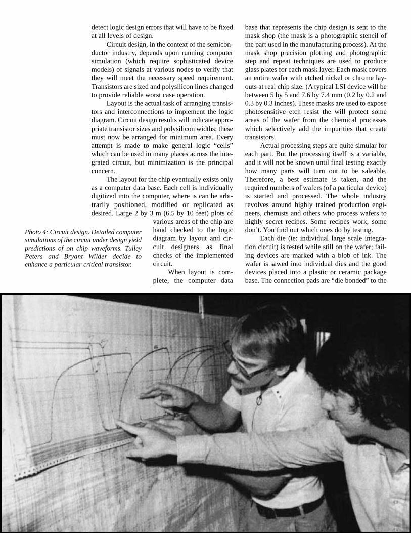
Photo 4: Circuit design. Detailed computersimulations of the circuit under design yieldpredictions of on chip waveforms. TulleyPeters and Bryant Wilder decide toenhance a particular critical transistor.

exposed internal lead frame with very tiny wire.The package is then sealed and tested again.
Testing a device having only 40 pins butwhich has up to 40,000 internal transistors is nomean trick nor a minor expense. Furthermore, thedevice must execute all operations properly at theworst case system conditions (which may be highor low extremes of temperature, voltage and load-ing) and work with other devices on a commonbus. Thus, the device is not specified to its ownmaximum operating speed, but rather the speed ofa worst case system. Motorola microprocessorscan usually be made to run much faster (and muchslower) than their guaranteed worst case specifica-tions.
Project Goals
The 6809 project started life with a numberof (mostly unformalized) goals. The principle pub-lic goal was to upgrade the 6800 processor to bedefinitely superior to the 8 bit competition. (TheMotorola 68000 project will address the 16 bitmarket with what we believe will be another supe-rior processor.) Many people, including many cus-tomers, felt that all that had to be done was to addanother index register (Y), a few supportinginstructions (LDY, STY) and correct some of thepast omissions (PSHX, PULX, PSHU,m PULY).Since this would mean a rather complete redesignanyway, it made little sense to stop there.
A more philosophical goal — thus one muchless useful in discussions with engineers and man-agers (who had their own opinions of what theproject should be) — was to minimize softwarecost. This led to an extensive, and thus hard toexplain sequence of logic that went somewhat likethis:
Q: How do we reduce software costs?A: 1. Write code is a block structured high
level language.2. Distribute the code in mass production
read only memories.Q: Why aren’t many read only memories
being used now?A: 1. The great opportunities for error in
assemble language allow many mistakes whichincur sever read only memory costs.
2. The present architecture is not suitablefor read only memories.
Q: In what way are the second generationprocessors unsuitable?
A: It is very difficult to use a read only mem-ory in any other context than that for which it wasoriginally developed. It is hard to use the sameread only memory on systems built by different
vendors. Simply having different input and output(IO) or using a different memory location is usual-ly enough to make the read only product useless.
Q: What is needed?A: 1. Position independent code.
2. Temporary variables on the stack.3. Indirect operations through the stack
for input and output.4. Absolute indirect operation for system
branch tables.
And so it went. How could we make a devicethat would answer the software problems of twogenerations of processors? How indeed!
Design Decisions
Usually an engineering project may be pur-sued in many ways, but only one way at a time.The ever present hope is that this one time will bethe only time necessary. Furthermore, it would benice to get the project over with as soon as possi-ble to get on with selling some products. (Arapidreturn on investment is especially important in atime of rapid inflation.) To these honorable endscertain decisions are made which delineate theinvestment and risk undertaken in an attempt toachieve a new product.
The 6809 project was no exception. To min-imize project risk it was decided that the 6809
Photo 5: Checking the flowcharts. Logic and circuit designer Bryant Wildercompares the specification to one of the flowcharts. The flowcharts are usedto develop Boolean equations for the required logic; those equations arethen used to generate a logic diagram.

would be built on the same technological base asthe recently completed 6800 depletion loadredesign. In particular, the machine would be arandom logic computer with essentially dynamicinternal operation. It would use the reliable 6800type of storage register. Functions would be com-patible with the defined 6800 bus and 6800 periph-erals. This decision would extend the like of partsalready in production and minimize testingperipheral devices for a particular processor (6800versus 6809). Buss compatibility doesn’t have tomean identity — the new device could have con-siderably improved specifications but could not doworse than the specifications for the existingdevice. This mandate was a little tricky when youconsider that we were dealing with a more com-plex device using exactly the same technology, butthere was a slight edge: the advancing very largescale integration (VLSI) learning curve.
One wide range decision wa that the newdevice would be an improved 6800 part. Thewidely known 6800 architecture would be iteratedand improved, but no radical departure would beconsidered. In fact, the new devise should be codecompatible with the 6800 at some level.
Compatibility was the basis for the 6809architecture design. It implied that the 6809 couldcapitalize on the existing familiarity with the
6800. 6800 programmers could be programmingfor the 6809 almost immediately and could learnand use new addressing mode and features as theywere needed. This decision also ended any consid-eration of radically new architecture for themachine before it was begun.
A corporation selling into a given market isnecessarily limited to moderate innovation. Anyvast product change requires reeducation of boththe internal marketing organization and the cus-tomer base before mass sales can proceed.Consequently, designers have to restrict their cre-ativity to conform to the market desires. Theamount of change actually implemented, producedand seen by society is the true meaning of a com-puter “generation.” In the end, society itselfdefines the limits of a new generation, and adesign years ahead of its time may well fail in themarketplace.
M6800 Data Analysis
Once the initial philosophical and marketingtrade-offs were made, construction of the finalform of the M6809 began. By this time a largenumbers of M6800 programs had been written byboth Motorola and our customers, so it was feltthat a good place to start design of the 6809 was toanalyze large amounts of existing 6800 sourcecode. Surprisingly, the data gathered about 6800usage of instructions and addressing modes agreedsubstantially with simular data previously com-piled for minicomputers and maxicomputers. Byfar the most common instructions were load andstores, which accounted for over 38 percent of all6800 instructions. Next were the subroutine calls(Direct, Extended, Immediate, Indexed, Relative,Accumulator) had nearly equal usage, which indi-cated that programmers actually took advantage ofthe bytes to be saved by direct (page zero) address-ing and indexed addressing. Furthermore the off-sets for indexed instructions were either 0 or lessthan 32 (see table 2).
This information was used to greatly expandthe addressing modes (as discussed later) with outmaking the 6800 programs require more codewhen converted to run on the 6809. Also the num-ber of increment or decrement index registerinstructions in loops indicated that autoincrement-ing and autodecrementing would be beneficial.
Auto decrementing and autoincrementing aresimular to indexing except the index registerused is decremented before, or decrementedafter, the addressing operation takes place.
As all programmers and even architectslike ourselves eventually learn, consistent anduniform instruction sets are used more effective-
Instruction Class Percent Usage
Loads 23.4Stores 15.3Subroutine calls and returns 13.0Conditional branches 11.0Unconditional branches and jumps 6.5Compares and tests 6.2Increments and decrements 6.1Clear 4.4Adds and subtracts 2.8All others 11.3
Table 1: 6800 instruction types based on static analysis of25,000 lines of 6800 source code. In static analysis theactual number of occurrences of each instruction is tal-lied from program listings. In the alternate technique,called dynamic analysis, the numbers of occurrences ofan instruction is tallied while the program is running. Aninstruction inside a program loop would therefore becounted more than once.
Table 2: Size of offsets used in6800 indexed addressing, basedon static analysis of 25,000 linesof 6800 source code.
Index Offset Percent Usage0 40.0
1-31 53.032-63 1.0
64-255 6.0

ly than instruction sets that treat similar resource(IO, registers or data) in dissimilar ways. Forexample, the least used instructions on the 6800were those that dealt with the A accumulator inspecific ways that did not apply to the B accumu-lator (eg: ABA: add B to A, CBA: compare B toA). It’s not that these instructions are not useful,it’s just that programmers will not use inconsistentinstructions or addressing modes. Consistencybecame the battle cry of the M6809 designers!
Customer Inputs
At the completion of the 6800 analysis stage,the first preliminary design specification for the6809 was generated. This preliminary specifica-tion was then taken to about 30 customers whorepresented a cross section of current 6800 users,as well as some customers and consultants knownto be hostile to the 6800. With these customers vis-its we hoped to resolve two major questions aboutthe 6809’s architecture:
1) Which architecture was more desirable 8bit or 16 bit?
2) Did 6809 compatibility with the 6800need to occur at the object level or at the sourcelevel.
Most customers felt that an 8 bit architecturewas adequate for their upcoming applications, andthey did not want to pay the price penalty for 16bit as long as the 6809 included the most common16 bit operations such as add, subtract, load, store,compare and multiply. Many were interestedthough, in Motorola’s advanced 16 bit processor(68000) for future 16 bit applications. From thevery inception of the6809 project it was a require-ment that the 6809 would be compatible with the6800. Wether this compatibility needed to occur atthe object level or at the assembly language(source code) level was a question we felt our cus-tomers should help us answer. Virtually every cus-tomer indicated that source compatibility was suf-ficient because they would not try to use 6800 readonly memories in 6809 systems. Most customersindicated that they would take advantage of the6800 compatibility in order to initially convertrunning 6800 programs into running 6809 pro-grams, and then modify the 6800 code to takeadvantage of the 6809’s features.
The decision not to be object code compati-ble was an easy one for us since it meant that wecould remap the 6800 op codes in a manner guar-anteed to produce more byte efficient and faster6809 programs. The remapping of op codes wasgreatly affected by the 6800 data analysis. Some
low occurrence 6800 instruction were combinedinto consistent 2 byte instructions, allowing themore useful instruction to take fewer bytes andexecute faster. Also, some 6800 instructions wereeliminated completely in favor of 2 instructionsequences. These sequences are generated auto-matically by our assembler when the 6800mnemonic is recognized. This remapping in favorof more often used functions results in 6809 pro-grams that require only one half to two thirds asmuch memory as 6800 programs, and run faster.
M6809 Registers
What, then, are the pertinent features thatmake the 6809 a next generation processor? In thefollowing paragraphs we will attempt to highlightthe improvements made to the 6800. The pro-gramming model for the 6809 (figure 1) consistsof four 8 bit registers and five 16 bit registers.
The A and B accumulators are the same asthose of the 6800 except that they can also be cate-nated into the A:B pair, called the D register, for16 bit operations.
The condition codes are simular to the 6800,with the inclusion of two new bits. The F bit is theinterrupt mask bit for the new fast interrupt. Thefast interrupt (FIRQ) only stacks the programcounter and condition code register when an inter-rupt occurs. The interrupt routine is then responsi-ble for stacking any registers it uses. The E bit is
X INDEX REGISTER
POINTER REGISTERS
Y INDEX REGISTER
U USER STACK POINTER
S HARDWARE STACK POINTER
PC PROGRAM COUNTER
A B
D
ACCUMULATORS
DP DIRECT PAGE REGISTER
CC–CONDITION CODE REGISTER
OVERFLOWCARRY–BORROW
ZERONEGATIVEINTERRUPT REQUEST MASKHALF CARRYFAST INTERRUPT REQUEST MASKENTIRE STATE ON STACK
E F H I N Z V C
Figure 1: 6809 programming model.
set when the registers are stacked during interruptsif the entire register set was saved (as in nonmask-able and maskable interrupts) or cleared if theshort register set was saved (for a fast interrupt).
On the 6800, an instruction with direct mode(or page zero) addressing consisted of an op codefollowed by an 8 bit value that defined the lowereight bits of an address, The upper eight bits werealways assumed to be zero. Thus, direct address-ing could only address locations in the lowest 256bytes of memory. The 6809 adds versatility to thisaddressing mode by defining an 8 bit direct pageregister that defines the upper eight bits of addressfor all direct addressing instructions. This allowsdirect mode addressing to be used throughout theentire address space of the machine. To maintain6800 compatibility, the direct page register is setto 0 on reset.
Four 16 bit indexable register are included inthe 6809. They are the X, Y, U and S registers. TheX register is the familiar 6800 index register, andthe S register is the hardware stack pointer. The Yregister is a second index register; the U register isthe user stack pointer. All four registers can beused in all indexing operations and the U and Sresisters are also stack pointers, The S register isused during interrupts and subroutine calls by thehardware to stack return addresses and machinestates.
The last 16 bit register is the program count-er. In certain 6809 addressing modes, the programcounter can also be used as an index register toachieve position independent code.
Addressing Modes
It was out opinion that the best way toimprove an existing architecture and maintainsource compatibility was to add powerful address-ing modes. In out view, the 6809 has the mostpowerful addressing modes available on anymicroprocessor. Powerful addressing modeshelped us achieve out goals of position independ-ence, reentrancy, recursion, consistency and easyimplementation of block structured high level lan-guages.
All the 6800 addressing modes (immediate,Extended, Direct, Indexed, Accumulator, Relative,and inherent) are supported on the 6809 with thedirect mode of addressing made more useful bythe inclusion of the direct page register (DPR).
The direct page register usage and directaddressing need some explanation, since they canbe very effective when used correctly. For exam-ple, since global variables are referenced frequent-ly in high level language execution, the direct pageregister can be used to point to a page containingthe global variables while the stack contains thelocal variables, which are also referenced fre-quently. This creates very efficient code which issafe since the compiler keeps track of the directpage register. The direct page register can also beused effectively and safely in a multitasking envi-ronment where the real time operating system
Type
Constantoffset from R
Accumulatoroffset from R
Autoincrement/–decrement R
Constant offsetfrom programcounter
Extended use nonindexed
Forms
no offset5 bit offset8 bit offset
16 bit offset
A register offsetB register offsetD register offset
increment by 1increment by 2decrement by 1decrement by 2
8 bit offset16 bit offset
Source
,Rn,Rn,Rn,R
A,RB,RD,R
,R+,R++,-R,--R
n,PCRn,PCR
Post Byte
Nonindirect
1RR001000RRnnnnn1RR010001RR01001
1RR001101RR001011RR01011
1R0000001RR000011RR000101RR00011
1XX011001XX01101
+~
0114
114
2323
15
+ #
0012
000
0000
12
Source
[,R]
[n,R][n,R]
[A,R][B,R][D,R]
[,R++]
[,--R]
[n,PCR][n,PCR]
[n]
Post Byte
Indirect
1RR10100defaults to 8-bit
1RR110001RR11001
1RR101101RR101011RR11011
not allowed1RR10001not allowed1RR10011
1XX111001XX11101
10011111
+~
3
47
447
6
6
48
5
+ #
0
12
000
0
0
12
2
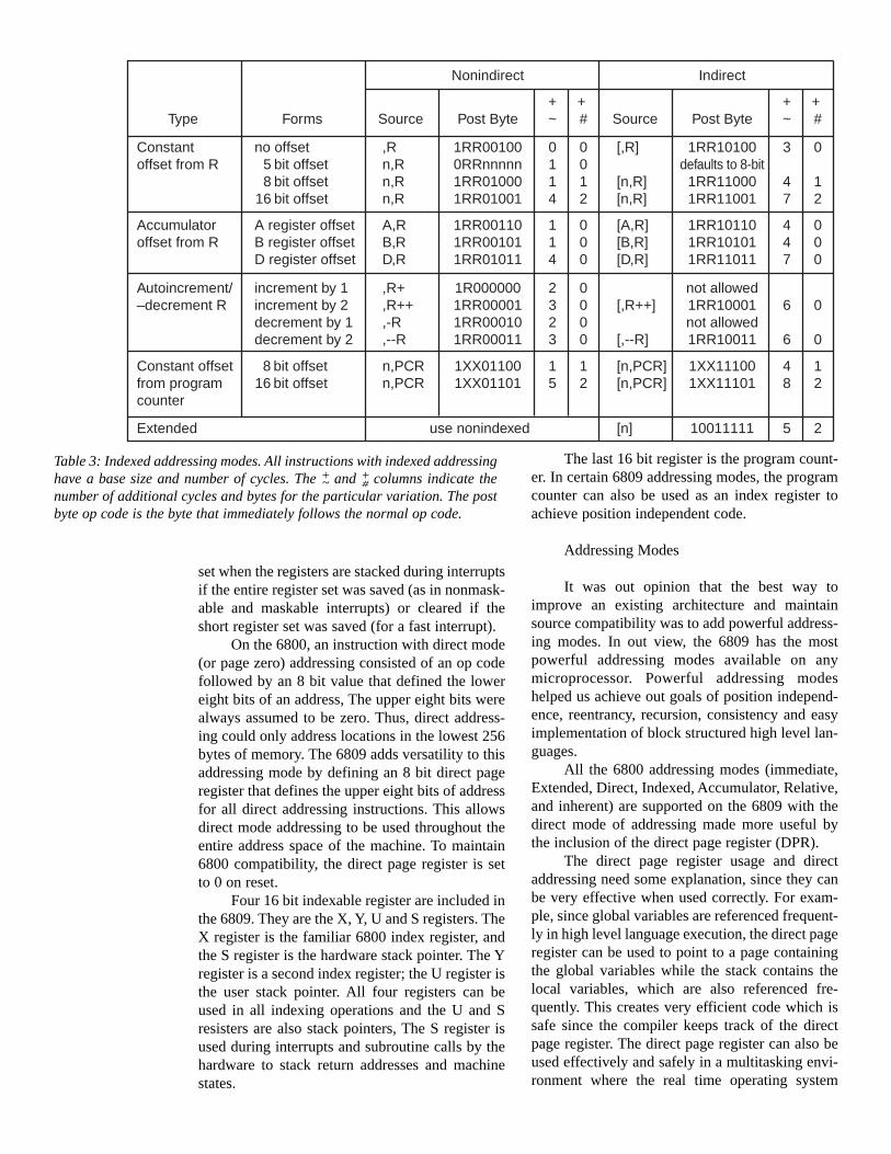
Table 3: Indexed addressing modes. All instructions with indexed addressinghave a base size and number of cycles. The +
~ and +# columns indicate thenumber of additional cycles and bytes for the particular variation. The postbyte op code is the byte that immediately follows the normal op code.
allocates a different base page register for eachtask.
On the other hand, it would be quite danger-ous to indiscriminately reallocate the direct pageregister frequently, such as within subroutines orloops, since it might become very easy to losetrack of the current direct page register value.Therefore, even though the direct page register isunstructured, we included it because, when usedcorrectly, the byte savings are significant. Also, tomake direct addressing more useful, the read mod-ify write instruction on the 6809 now have allmemory addressing modes: Direct, Extended andIndexed.
The major improvements in the 6809’saddressing mode were made by greatly expandingthe indexed addressing modes as well as makingall indexable instructions applicable to the X, Y, Uand S registers (see table 3).
Indexed addressing with an offset is familiarto 6800 users, but the 6809 allows the offset to beany of four possible lengths: 0, 5, 8 or 16 bits, andthe offsets are signed two’s complements values.This allows greater flexibility in addressing while
achieving maximum byte efficiency. The inclusionof the 16 bit offset allows the role of index regis-ter and offset to be reversed if desired. A furtherenhancement allows all of the above modes toinclude an additional level of indirection. Evenextended addressing can be indirected (as a specialindexed addressing mode). Since either stackpointer can be specified as a base address inindexed addressing, the indirect mode allowsaddresses of data to be passed to a subroutine. Thesubroutine can then reference the data pointed towith one instruction. This increases the efficiencyof high level language calls that pass arguments byreference.
M6800 data indicated that quite often theindex register was being used in a loop and incre-mented or decremented each time. This moved thepointer though tables or was used to move datafrom one area of memory to another (blockmoves). Therefore, we implemented autoincre-ment and autodecrement indexed addressing in theM6809. In autoincrement mode the value pointedto by the index register is used as the effectiveaddress, and then the index register is increment-
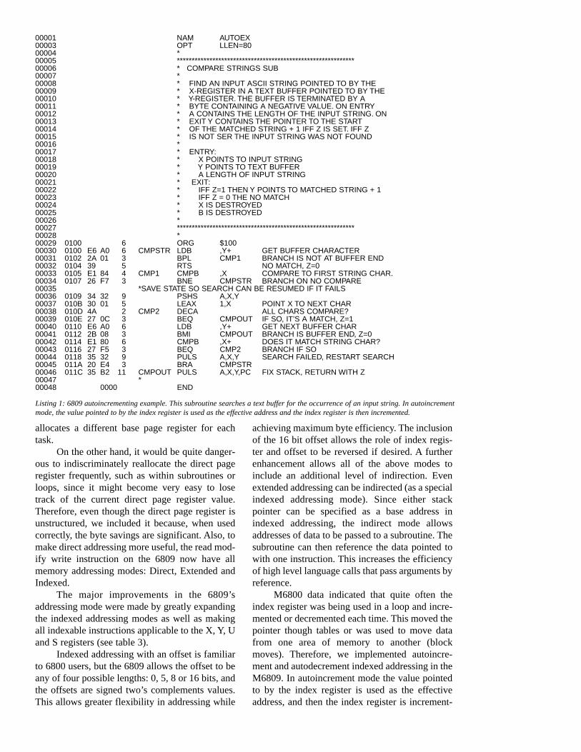
00001 NAM AUTOEX00003 OPT LLEN=8000004 *00005 ************************************************************00006 * COMPARE STRINGS SUB00007 *00008 * FIND AN INPUT ASCII STRING POINTED TO BY THE00009 * X-REGISTER IN A TEXT BUFFER POINTED TO BY THE00010 * Y-REGISTER. THE BUFFER IS TERMINATED BY A00011 * BYTE CONTAINING A NEGATIVE VALUE. ON ENTRY00012 * A CONTAINS THE LENGTH OF THE INPUT STRING. ON00013 * EXIT Y CONTAINS THE POINTER TO THE START00014 * OF THE MATCHED STRING + 1 IFF Z IS SET. IFF Z00015 * IS NOT SER THE INPUT STRING WAS NOT FOUND00016 *00017 * ENTRY:00018 * X POINTS TO INPUT STRING00019 * Y POINTS TO TEXT BUFFER00020 * A LENGTH OF INPUT STRING00021 * EXIT:00022 * IFF Z=1 THEN Y POINTS TO MATCHED STRING + 100023 * IFF Z = 0 THE NO MATCH00024 * X IS DESTROYED00025 * B IS DESTROYED00026 *00027 ************************************************************00028 *00029 0100 6 ORG $10000030 0100 E6 A0 6 CMPSTR LDB ,Y+ GET BUFFER CHARACTER00031 0102 2A 01 3 BPL CMP1 BRANCH IS NOT AT BUFFER END00032 0104 39 5 RTS NO MATCH, Z=000033 0105 E1 84 4 CMP1 CMPB ,X COMPARE TO FIRST STRING CHAR.00034 0107 26 F7 3 BNE CMPSTR BRANCH ON NO COMPARE00035 *SAVE STATE SO SEARCH CAN BE RESUMED IF IT FAILS00036 0109 34 32 9 PSHS A,X,Y00037 010B 30 01 5 LEAX 1,X POINT X TO NEXT CHAR00038 010D 4A 2 CMP2 DECA ALL CHARS COMPARE?00039 010E 27 0C 3 BEQ CMPOUT IF SO, IT’S A MATCH, Z=100040 0110 E6 A0 6 LDB ,Y+ GET NEXT BUFFER CHAR00041 0112 2B 08 3 BMI CMPOUT BRANCH IS BUFFER END, Z=000042 0114 E1 80 6 CMPB ,X+ DOES IT MATCH STRING CHAR?00043 0116 27 F5 3 BEQ CMP2 BRANCH IF SO00044 0118 35 32 9 PULS A,X,Y SEARCH FAILED, RESTART SEARCH00045 011A 20 E4 3 BRA CMPSTR00046 011C 35 B2 11 CMPOUT PULS A,X,Y,PC FIX STACK, RETURN WITH Z00047 *00048 0000 END
Listing 1: 6809 autoincrementing example. This subroutine searches a text buffer for the occurrence of an input string. In autoincrementmode, the value pointed to by the index register is used as the effective address and the index register is then incremented.
ed. Autodecrement is similar except that the indexregister is first decremented and then used toobtain the effective address. Listing 1 is an exam-ple of a subroutine that searches a text; buffer forthe occurrence of an input string. It makes heavyuse of autoincrementing.
Since the 6809 supports 8 and 16 bit opera-tions, the size of the increment or decrement canbe selected by the programmer to be 1 or 2. Thepost increment, predecrement nature of theaddressing mode makes it equivalent in operationto a push and pull from a stack. This allows the Xand Y registers to also be used as software stackpointers if the programmer needs more than twostacks. All indexed addressing modes can alsocontain an extra level of post indirection.Autoincrement and autodecrement are more versa-tile than the block moves and string commandsavailable on other processors.
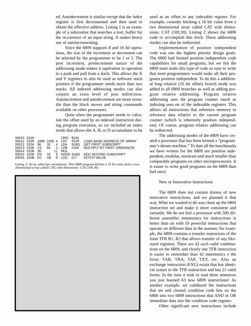
Quite often the programmer needs to calcu-late the offset used by an indexed instruction dur-ing program execution, so we included an indexmode that allows the A, B, or D accumulator to be
used as an offset to any indexable register. Forexample, consider fetching a 16 bit value from atwo dimensional array called CAT with dimen-sions: CAT (100,30). Listing 2 shows the 6809code to accomplish this fetch. These addressingmodes can also be indirected.
Implementation of position independentcode was one the highest priority design goals.The 6800 had limited position independent codecapabilities for small programs, but we felt the6809 must make this type of code so easy to writethat most programmers would make all their pro-grams position independent. To do this a addition-al long relative (16 bit offset) branch mode wasadded to all 6800 branches as well as adding pro-gram relative addressing. Program relativeaddressing uses the program counter much asindexing uses on of the indexable registers. Thisallows all instructions that reference memory toreference data relative to the current programcounter (which is inherently position independ-ent). Of course, program relative addressing canbe indirected.
The addressing modes of the 6809 have cre-ated a processor that has been termed a “program-mer’s dream machine.” To date all the benchmarkswe have written for the 6809 are position inde-pendent, modular, reentrant and much smaller thancomparable programs on other microprocessors. Itis easier to write good programs on the 6809 thanbad ones!
New or Innovative Instructions
The 6809 does not contain dozens of newinnovative instructions, and we planned it thatway. What we wanted to do was clean up the 6800instruction set and make it more consistent andversatile. We do not feel a processor with 500 dif-ferent assembler mnemonics for instructions isbetter than on with 59 powerful instructions thatoperate on different data in the manner, for exam-ple, the 6809 contains a transfer instruction of theform TFR R1, R2 that allows transfer of any like-sized registers. There are 42 such valid combina-tions on the 6809, and clearly one TFR instructionis easier to remember than 42 mnemonics o theform: TAB, TBA, TAP, TXY, etc. Also anexchange instruction (EXG) exists that has identi-cal syntax to the TFR instruction and has 21 validforms. In the time it took to read three sentencesyou just learned 63 new 6809 instructions! Asanother example, we combined the instructionsthat set and cleared condition code bits on the6800 into two 6809 instructions that AND or ORimmediate data into the condition code register.
Other significant new instructions include
00010 0100 ORG $10000011 0100 108E 1000 4 LDY #CAT LOAD BASE ADDRESS OF ARRAY00012 0104 96 32 4 LDA SUB1 GET FIRST SUBSCRIPT00013 0106 C6 64 2 LDB #100 MULTIPLY BY FIRST DIMENSION00014 0108 3D 11 MUL00015 0109 D3 33 6 ADDD SUB2 ADD SECOND SUBSCRIPT00016 010B EC AB 9 LDD D,Y FETCH VALUE
Listing 2: Array subscript calculations. This 6809 program fetches a 16 bit value from a two-dimensional array called CAT, with dimensions: CAT (100,30).
the new 16 bit operations, The D register can beloaded, stored, added to subtracted from, com-pared, transferred, exchanged, pushed and pulled.All the indexable registers (16 bits) and be loaded,stored and compared. The load effective addressinstruction can also be used to perform 8 or 16 bitarithmetic on the indexable registers as describedlater.
Two significant new instructions are the mul-tiple push and multiple instructions on the 6809.With one 2 byte instruction any register or set ofregisters can be pushed or pulled from witherstack. These instructions greatly decrease theoverhead associated with subroutine calls in bothassembly and high level language programs. Inconjunction with instructions using autoincrementand autodecrement, the 6809 can efficiently emu-late a stack computer architecture, which means itshould e efficient for Pascal p-code interpretersand the like.
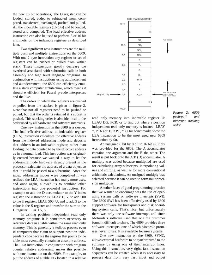
The orders in which the registers are pushedor pulled from the stacked is given in figure 2.Note that not all registers need to be pushed orpulled, but that the order is retained if a subset ispushed. This stacking order is also identical to theorder used by all hardware and software interrupts.
One new instruction in the 6809 is a sleeper.The load effective address to indexable register(LEA) instruction calculates the effective addressfrom the indexed addressing mode and depositsthat address in an indexable register, rather thanloading the data pointed to by the effective addressas in a normal load. This instruction was original-ly created because we wanted a way to let theaddressing mode hardware already present in theprocessor calculate the address of a data object sothat it could be passed to a subroutine. After theindex addressing modes were completed it wasrealized the LEAinstruction had many more uses,and once again, allowed us to combine otherinstructions into one powerful instruction. Forexample to add the D accumulator to the Y indexregister, the instruction is: LEAY D, Y; to add 500to the U register: LEAU 500, U; and to add 5 to thevalue is the S register and transfer the sum to theU register: LEAU 5, S.
In writing position independent read onlymemory programs it is sometimes necessary toreference data in a table within the same read onlymemory. This is generally a tedious process evenin computers that claim to support position inde-pendent code because the register that points to thetable must eventually contain an absolute address.The LEAinstruction, in conjunction with programcounter relative addressing, makes this possiblewith one instruction on the 6809. For example, toput the address of a table DG located in a relative
read only memory into indexable register U:LEAU DG, PCR; or to find out where a positionindependent read only memory is located: LEAY*, PCR (or TFR PC, Y). Our benchmarks show theLEA instruction to be the most used new 6809instruction by far.
An unsigned 8 bit by 8 bit to 16 bit multiplywas provided for the 6809. The A accumulatorcontains one argument and the B the other. Theresult is put back onto the A:B (D) accumulator. Amultiply was added because multiplied are usedfor calculating array subscripts, interpolating val-ues and shifting, as well as for more conventionalarithmetic calculations. An unsigned multiply wasselected because it can be used to form multipreci-sion multiplies.
Another facet of good programming practicethat we wanted to encourage was the use of oper-ating system calls or software interrupts (SWI).The 6800 SWI has been effectively used by 6800support software for breakpoints and disk operat-ing system calls. That’s nice, but unfortunatelythere was only one software interrupt, and sinceMotorola’s software used that one the customerfound it difficult to share. The 6809 provides threesoftware interrupts, one of which Motorola prom-ises never to use. It is available for user systems.
One new instruction on the 6809, SYNC,allows external hardware to be synchronized to thesoftware by using one of their interrupt lines.Using this instruction, very tight, fast instructionsequences can be created when it is necessary toprocess data from very fast input and output
6809 STACKING ORDER
PUSH ORDER
PULL FROM STACKTOP OF STACKPUSH ONTO STACK
FFFF
0000
10,S
PCL
PCH
U/SL
U/SH
YL
YH
XL
XH
DPR
B
A
CCR
8,S
6,S
4,S
3,S
2,S
1,S
0,SSP (OR US)
Figure 2: 6809push/pull andinterrupt stackingorder.
devices. Listing 4 gives an example of the use ofSYNC. It is assumed that the A side of the periph-eral interface adapter (PIA) is connected to a highspeed device that transfers 128 bytes of data to amemory buffer. When the device is ready to senda piece of data, it generates a fast interrupt (FIRQ)from the A side of the peripheral interface adapter.Program lines 12 and 13 set up the transfer; lines16 through 20 are the synchronization loop. Oneach pass through the loop, the program waits atthe SYNC instruction until any interrupt line ispulled low. When the interrupt line goes low, theprocessor executed the next instruction. In order touse SYNC, all other devices tied to any of theinterrupt line must be disabled. For this example itwas assumed that the B side of the peripheralinterface adapter also had interrupts enabled; pro-gram lines 9 though 11 disable the interrupts andline 21 through 23 reenable it. Line 14 is includedto keep the interrupt by the A side of the peripher-al interface adapter from going to the interruptroutine. Note that interrupts do not need to beenabled for SYNC to work, and in fact are nor-mally disabled.
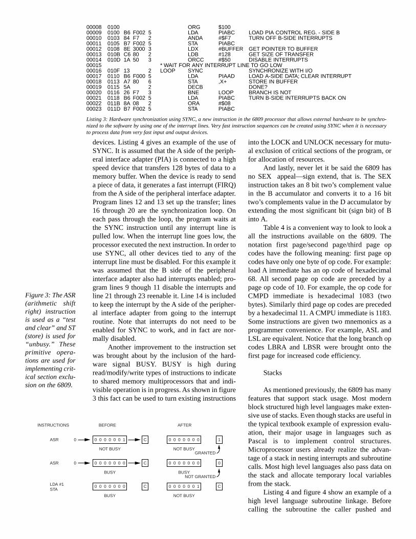
Another improvement to the instruction setwas brought about by the inclusion of the hard-ware signal BUSY. BUSY is high duringread/modify/write types of instructions to indicateto shared memory multiprocessors that and indi-visible operation is in progress. As shown in figure3 this fact can be used to turn existing instructions
into the LOCK and UNLOCK necessary for mutu-al exclusion of critical sections of the program, orfor allocation of resources.
And lastly, never let it be said the 6809 hasno SEX appeal—sign extend, that is. The SEXinstruction takes an 8 bit two’s complement valuein the B accumulator and converts it to a 16 bittwo’s complements value in the D accumulator byextending the most significant bit (sign bit) of Binto A.
Table 4 is a convenient way to look to look aall the instructions available on the 6809. Thenotation first page/second page/third page opcodes have the following meaning: first page opcodes have only one byte of op code. For example:load A immediate has an op code of hexadecimal68. All second page op code are preceded by apage op code of 10. For example, the op code forCMPD immediate is hexadecimal 1083 (twobytes). Similarly third page op codes are precededby a hexadecimal 11. A CMPU immediate is 1183.Some instructions are given two mnemonics as aprogrammer convenience. For example, ASL andLSL are equivalent. Notice that the long branch opcodes LBRAand LBSR were brought onto thefirst page for increased code efficiency.
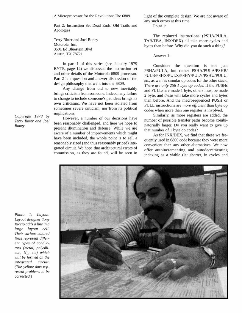
Stacks
As mentioned previously, the 6809 has manyfeatures that support stack usage. Most modernblock structured high level languages make exten-sive use of stacks. Even though stacks are useful inthe typical textbook example of expression evalu-ation, their major usage in languages such asPascal is to implement control structures.Microprocessor users already realize the advan-tage of a stack in nesting interrupts and subroutinecalls. Most high level languages also pass data onthe stack and allocate temporary local variablesfrom the stack.
Listing 4 and figure 4 show an example of ahigh level language subroutine linkage. Beforecalling the subroutine the caller pushed and
00008 0100 ORG $10000009 0100 B6 F002 5 LDA PIABC LOAD PIA CONTROL REG. - SIDE B00010 0103 84 F7 2 ANDA #$F7 TURN OFF B-SIDE INTERRUPTS00011 0105 B7 F002 5 STA PIABC00012 0108 8E 3000 3 LDX #BUFFER GET POINTER TO BUFFER00013 010B C6 80 2 LDB #128 GET SIZE OF TRANSFER00014 010D 1A 50 3 ORCC #$50 DISABLE INTERRUPTS00015 * WAIT FOR ANY INTERRUPT LINE TO GO LOW00016 010F 13 2 LOOP SYNC SYNCHRONIZE WITH I/O00017 0110 B6 F000 5 LDA PIAAD LOAD A-SIDE DATA; CLEAR INTERRUPT00018 0113 A7 80 6 STA ,X+ STORE IN BUFFER00019 0115 5A 2 DECB DONE?00020 0116 26 F7 3 BNE LOOP BRANCH IS NOT00021 0118 B6 F002 5 LDA PIABC TURN B-SIDE INTERRUPTS BACK ON00022 011B 8A 08 2 ORA #$0800023 011D B7 F002 5 STA PIABC
Listing 3: Hardware synchronization using SYNC, a new instruction in the 6809 processor that allows external hardware to be synchro-nized to the software by using one of the interrupt lines. Very fast instruction sequences can be created using SYNC when it is necessaryto process data from very fast input and output devices.
INSTRUCTIONS
ASR 0 C0 0 0 0 0 0 1
BEFORE
NOT BUSY
10 0 0 0 0 0 0
NOT BUSYGRANTED
NOT GRANTED
00 0 0 0 0 0 0
BUSY
C0 0 0 0 0 0 1
NOT BUSY
AFTER
ASR 0 C0 0 0 0 0 0 0
BUSY
LDA #1STA
C0 0 0 0 0 0 0
BUSY
Figure 3: The ASR(arithmetic shiftright) instructionis used as a “testand clear” and ST(store) is used for“unbusy.” Theseprimitive opera-tions are used forimplementing crit-ical section exclu-sion on the 6809.

addresses of two arguments and the answer on thestack and then executed the jump to subroutinewhich puts the return program counter on thestack. The subroutine then saves the old stackmark pointer on the stack as well as reservingspace on the stack for the local variables for thesubroutine. In this example, size locations are usedbut the subroutine body during calculation. At thispoint the stack mark pointer is set to a new valuefor this subroutine. The stack mark pointer is usedbecause the S register may very during executionof the subroutine body due to local subroutines,etc. It is much more convenient for the compiler togenerate offsets to the parameters is the U is usedfor this purpose instead of the S.
Once U is set it is used to fetch the two argu-ments using indexed indirect addressing. The sub-
routine body presumable does something with thearguments and finishes with an answer in the Dregister. The subroutine exit saved this value. Itthen puts the return address in X and restores theprevious stack mark pointer. The whole stack isthen cleaned up (deleted) and return is made to thecaller.
Motorola 6800 users should note that thestack pointers on the 6809 point to the last valuepushed on the stack rather than the next free loca-tion, as on the 6800. This was done so that autoin-crement and autodecrement would be equivalentto pulls and pushes. For example: STA ,-S isequivalent to PSHS A; and LDA,S+ is equivalentto PULS S. This also means the X and Y registerscan be used as stack pointers if the programmerdesires. For example: STA ,-X is a push on a stack
Table 4: 6809 op code map and cycle counts. The numbers by each op code indicate the number of machine cycles required to executeeach instruction. When the number contains an I (eg: 4+I), and additional number of machine cycles equaling I may be required (seetable 3). The presence of two numbers, with the second on in parentheses, indicate that the instruction involves a branch. The largernumber applies if the branch is taken. The notation first page/second page/third page has the following meaning: first page op codeshave only one bye of op code (eg: load A immediate has an op code of hexadecimal 86). All page 2 op codes are preceded by a pageop code hexadecimal 10 (eg: the op code for CMPD immediate is hexadecimal 1083 – two bytes). Similarly third page op codes arepreceded by a hexadecimal 11. A CMPU immediate is 1183. Some instructions are given two mnemonics as a programmer convenience(eg ASLand LSLare equivalent). Notice that the long branch op codes LBRAand LBSR were brought onto the first page to increasedcode efficiency.
Most Significant Four Bits
Leas
t Sig
nific
ant F
our
Bits
DIR REL ACCA ACCB IND EXT IMM DIR IND EXT IMM DIR IND EXT
0000 0001 0010 0011 0100 0101 0110 0111 1000 1001 1010 1011 1100 1101 1110 1111
1
6NEG0000 0
0001 1
0010 2
0011 3
0100 4
0101 5
0110 6
0111 7
1000 8
1001 9
1010 A
1011 B
1100 C
1101 D
1110 E
1111 F
0
1
2
3
4
5
6
7
8
9
A
B
C
D
E
F
6COM
6LSR
6ROR
6ASR
6 ASL(LSL)
6ROL
6DEC
6INC
6TST
3JMP
6CLR
4+ILEAX
2 2 6+I 7NEG
2 4 4+I 5SUBA
2 4 4+I 5SUBB
2 4 4+I 5CMPB
2 4 4+I 5SBCB
2 4 4+I 5ADDD
2 4 4+I 5ANDB
2 4 4+I 5BITB
2 4 4+I 5LDB
2 4 4+I 5EORB
2 4 4+I 5ADCB
2 4 4+I 5ORB
2 4 4+I 5ADDB
3 5 5+I 6LDD
5 5+I 6STD
4 4+I 5STB
2 4 4+I 5CMPA
2 4 4+I 5SBCA
2 4 4+I 5ANDA
2 4 4+I 5BITA
2 4 4+I 5LDA
2 4 4+I 5EORA
2 4 4+I 5ADCA
2 4 4+I 5ORA
2 4 4+I 5ADDA
7 7 7+I 8 BSR JSR
4 4+I 5STA
4,6,6+I,7 5,7,7+I,8 5,7,7+I,8SUBD CMPD CMPU
2 2 6+I 7COM
2 2 6+I 7LSR
2 2 6+I 7ROR
2 2 6+I 7ASR
2 2 6+I 7ASL (LSL)
2 2 6+I 7ROL
2 2 6+I 7DEC
2 2 6+I 7INC
2 2 6+I 7TST
2 2 6+I 7CLR
3+I 4 JMP
4+ILEAY
4+ILEAS
4+ILEAU
5+1/byPSHS
5+1/byPULS
5+1/byPSHU
5+1/byPULU
5RTS
3ABX
6/15RTI
20CWAI
11MUL
19/20/20SWI/2/3
3 BRA
3 BRN/5 LBRN
3 BHI/5(6)LBHI
3 BLS/5(6) LBHS
3 BHS5(6) BCC
3 BLO/5(6) (BCS)
3 BNE/5(6) LBNE
3 BEQ/5(6) LBEQ
3 BVC/5(6) LBVC
3 BVS/5(6) LBVS
3 BPL/5(6) LBPL
3 BMI/5(6) LBMI
3 BGE/5(6) LBGE
3 BLT/5(6) LBLT
3 BGT/5(6) LBGT
3 BLE/5(6) LBLE
PAGE2
PAGE3
2NOP
2SYNC
5LBRA
9LBSR
2DAA
3ORCC
3ANDCC
2SEX
8EXG
7TFR
2 3 4 5 6 7 8 9 A B C D E F F
4,6,6+I,7 5,7,7+I,8 5,7,7+I,8CMPX CMPY CMPS
3,5,5+I,6 4,6,6+I,7LDX LDY
3,5,5+I,6 4,6,6+I,7LDU LDS
5,5+I,6 6,6+I,7STX STY
5,5+I,6 6,6+I,7STU STS
defined by X. The possible ambiguity betweenwhere the stack pointer points on the 6800 and the6809 may be less of a problem than it seems, sinceof 6800’s TSX becomes the 6809’s TFR S, Xwithout adding 1 and TXS becomes a TFR X, Swithout subtracting 1 – think about it. The onlydanger is in programs that used the stack pointer asan index register. In these programs the stackpointer may point on location away from where itdid previously.
Interrupts
The 6809 has three fully vectored hardwareinterrupts. The nonmaskable interrupt (NMI) andmaskable interrupt (IRQ) are the same as the6800’s NMI and IRQ. The new interrupt is the fastmaskable interrupt, or FIRQ, that stacks the pro-gram counter and condition code register only oninterrupt. Table 5 gives the addresses of the inter-rupt vectors for the 6809.
A new signal (IACK) has been added that isavailable anytime an interrupt vector is fetched.This signal together with address bus lined A1through A3 can be used to implement in interruptscheme in which each device supplies its owninterrupt vector.
The interrupt control and prioritization logicof the 6809 have been defined very carefully – notredundant or indeterminate conditions can existwhen several interrupts occur simultaneously. Thedetails of the interrupt structure are preciselydefined in Motorola documentation for the 6809.
Part 2, entitled “instruction Set Dead-Ends,Old Trails and Apologies,” will be a question andanswer discussion about the design philosophythat went into the 6809.■
Table 5: Hexadecimaladdresses of the 6809restart and interrupt vec-tors.
FFFF RestartFFFC NMIFFFA SWIFFF8 IRQFFF6 FIRQFFF4 SWI2FFF2 SWI3FFF0 Reserved
14
12
10
8
6
5
4
3
2
1
0
OFFSET FROMSTACK MARK(U)
ADDRESS
OF ARG 1
ADDRESS
OF ARG 2
ADDRESS
OF ANS
RETURN
PC'
OLD STACK
MARK (U')
LOCAL
VARIABLES
U'
S'
U
S
00006 0500 34 40 6 SUBR PSHS U SAVE OLD STACK MARKER00007 0502 32 66 5 LEAS 6,S RESERVE LOCAL STORAGE00008 0504 1F 43 6 TFR S,U GET NEW STACK MARKER00009 0506 EC D8 0E 10 LDD [14,U] GET ARGUMENT 100010 0509 AE DE 0C 10 LDX [12,U] GET ARGUMENT 200011 *00012 * SUBROUTINE BODY00013 *00014 050C ED D3 0A 10 STD [10,U] SAVE ANSWER00015 050F AE 48 6 LDX 8,U GET RETURN ADDRESS00016 0511 EE 46 6 LDU 6,U RESTORE U’00017 0513 32 E8 10 6 LEAS 16,S POP EVERYTHING OFF STACK00018 0516 6E 84 3 JMP ,X RETURN
Listing 4: Use of stacks on the 6809 processor. In this typical high level language subroutine example, U’and S’are the mark stack point-er and the hardware stack pointer, respectively, just prior to the call. U and S are the same registers during execution of the subroutinebody. Before calling the subroutine the caller pushes the address of two arguments and the answer on the stack and then executes the jumpto subroutine which puts the return program counter on the stack. The subroutine then saves the old stack mark pointer on the stack aswell as reserving space on the stack for the local variables for the subroutine (see figure 4).

A Microprocessor for the Revolution: The 6809
Part 2: Instruction Set Dead Ends, Old Trails andApologies
Terry Ritter and Joel BoneyMotorola, Inc.3501 Ed Bluestein BlvdAustin, TX 78721
In part 1 of this series (see January 1979BYTE, page 14) we discussed the instruction setand other details of the Motorola 6809 processor.Part 2 is a question and answer discussion of thedesign philosophy that went into the 6809.
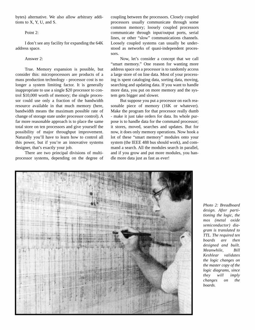
Any change from old to new inevitablybrings criticism from someone. Indeed, any failureto change to include someone’s pet ideas brings itsown criticisms. We have not been isolated fromsometimes severe criticism, nor from its politicalimplications.
However, a number of our decisions havebeen reasonably challenged, and here we hope topresent illumination and defense. While we areaware of a number of improvements which mighthave been included, the whole point is to sell areasonably sized (and thus reasonably priced) inte-grated circuit. We hope that architectural errors ofcommission, as they are found, will be seen in
light of the complete design. We are not aware ofany such errors at this time.
Point 1:
The replaced instructions (PSHA/PULA,TAB/TBA, INX/DEX) all take more cycles andbytes than before. Why did you do such a thing?
Answer 1:
Consider: the question is not justPSHA/PULA, but rather PSHA/PULA/PSHB/PULB/PSHX/PULX/PSHY/PULY/PSHU/PULU,etc, as well as simular op codes for the other stack.There are only 256 1 byte op codes. If the PUSHsand PULLs are made 1 byte, others must be made2 byte, and thesewill take more cycles and bytesthan before. And the macrosequenced PUSH orPULL instructions are more efficientthan byte opcodes when more than one register is involved.
Similarly, as more registers are added, thenumber of possible transfer paths become combi-natorially larger. Do you really want to give upthat number of 1 byte op codes?
As for INX/DEX, we find that these we fre-quently used in 6800 code because they were moreconvenient than any other alternatives. We nowoffer autoincrementing and autodecrementingindexing as a viable (ie: shorter, in cycles and
Photo 1: Layout.Layout designer TonyRiccio adds a line in alarge layout cell.Their various coloredlines represent differ-ent types of conduc-tors (metal, polysili-con, N_, etc) whichwill be formed on theintegrated circuit.(The yellow dots rep-resent problems to becorrected.)
Copyright 1978 byTerry Ritter and JoelBoney
bytes) alternative. We also allow arbitrary addi-tions to X, Y, U, and S.
Point 2:
I don’t see any facility for expanding the 64Kaddress space.
Answer 2:
True. Memory expansion is possible, butconsider this: microprocessors are products of amass production technology - processor cost is nolonger a system limiting factor. It is generallyinappropriate to use a single $20 processor to con-trol $10,000 worth of memory; the single proces-sor could use only a fraction of the bandwidthresource available in that much memory (here,bandwidth means the maximum possible rate ofchange of storage state under processor control). Afar more reasonable approach is to place the sametotal store on ten processors and give yourself thepossibility of major throughput improvement.Naturally you’ll have to learn how to control allthis power, but if you’re an innovative systemsdesigner, that’s exactly your job.
There are two principal divisions of multi-processor systems, depending on the degree of
coupling between the processors. Closely coupledprocessors usually communicate through somecommon memory; loosely coupled processorscommunicate through input/output ports, seriallines, or other “slow” communications channels.Loosely coupled systems can usually be under-stood as networks of quasi-independent proces-sors.
Now, let’s consider a concept that we call“smart memory.” One reason for wanting moreaddress space on a processor is to randomly accessa large store of on line data. Most of your process-ing is spent cataloging data, sorting data, moving,searching and updating data. If you want to handlemore data, you put on more memory and the sys-tem gets bigger and slower.
But suppose you put a processor on each rea-sonable piece of memory (16K or whatever).Make the program for that processor really dumb- make it just take orders for data. Its whole pur-pose is to handle data for the command processor;it stores, moved, searches and updates. But fornow, it does only memory operations. Now hook alot of these “smart memory” modules onto yoursystem (the IEEE 488 bus should work), and com-mand a search. All the modules search in parallel,and if you grow and put more modules, you han-dle more data just as fast as ever!
Photo 2: Breadboarddesign. After parti-tioning the logic, themos (metal oxidesemiconductor) dia-gram is translated toTTL. The required tenboards are thendesigned and built.Meanwhile, BillKeshlear validatesthe logic changes onthe master copy of thelogic diagrams, sincethey will implychanges on theboards.
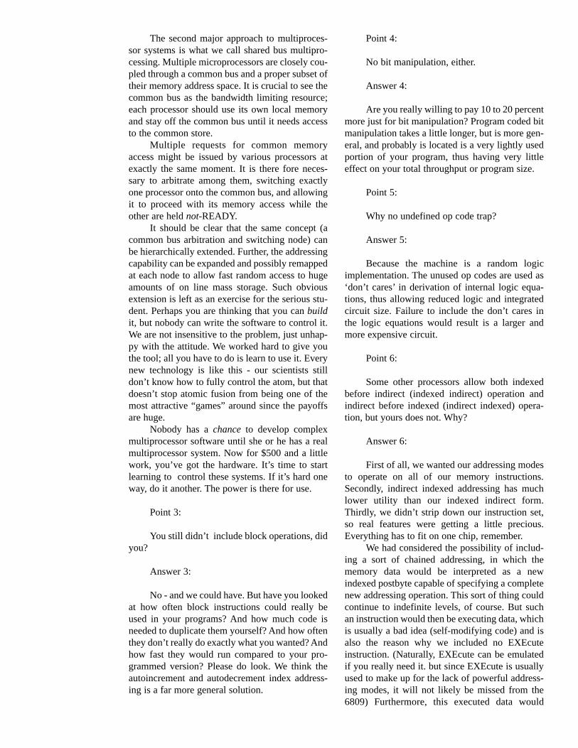
The second major approach to multiproces-sor systems is what we call shared bus multipro-cessing. Multiple microprocessors are closely cou-pled through a common bus and a proper subset oftheir memory address space. It is crucial to see thecommon bus as the bandwidth limiting resource;each processor should use its own local memoryand stay off the common bus until it needs accessto the common store.
Multiple requests for common memoryaccess might be issued by various processors atexactly the same moment. It is there fore neces-sary to arbitrate among them, switching exactlyone processor onto the common bus, and allowingit to proceed with its memory access while theother are held not-READY.
It should be clear that the same concept (acommon bus arbitration and switching node) canbe hierarchically extended. Further, the addressingcapability can be expanded and possibly remappedat each node to allow fast random access to hugeamounts of on line mass storage. Such obviousextension is left as an exercise for the serious stu-dent. Perhaps you are thinking that you can buildit, but nobody can write the software to control it.We are not insensitive to the problem, just unhap-py with the attitude. We worked hard to give youthe tool; all you have to do is learn to use it. Everynew technology is like this - our scientists stilldon’t know how to fully control the atom, but thatdoesn’t stop atomic fusion from being one of themost attractive “games” around since the payoffsare huge.
Nobody has a chanceto develop complexmultiprocessor software until she or he has a realmultiprocessor system. Now for $500 and a littlework, you’ve got the hardware. It’s time to startlearning to control these systems. If it’s hard oneway, do it another. The power is there for use.
Point 3:
You still didn’t include block operations, didyou?
Answer 3:
No - and we could have. But have you lookedat how often block instructions could really beused in your programs? And how much code isneeded to duplicate them yourself? And how oftenthey don’t really do exactly what you wanted? Andhow fast they would run compared to your pro-grammed version? Please do look. We think theautoincrement and autodecrement index address-ing is a far more general solution.
Point 4:
No bit manipulation, either.
Answer 4:
Are you really willing to pay 10 to 20 percentmore just for bit manipulation? Program coded bitmanipulation takes a little longer, but is more gen-eral, and probably is located is a very lightly usedportion of your program, thus having very littleeffect on your total throughput or program size.
Point 5:
Why no undefined op code trap?
Answer 5:
Because the machine is a random logicimplementation. The unused op codes are used as‘don’t cares’in derivation of internal logic equa-tions, thus allowing reduced logic and integratedcircuit size. Failure to include the don’t cares inthe logic equations would result is a larger andmore expensive circuit.
Point 6:
Some other processors allow both indexedbefore indirect (indexed indirect) operation andindirect before indexed (indirect indexed) opera-tion, but yours does not. Why?
Answer 6:
First of all, we wanted our addressing modesto operate on all of our memory instructions.Secondly, indirect indexed addressing has muchlower utility than our indexed indirect form.Thirdly, we didn’t strip down our instruction set,so real features were getting a little precious.Everything has to fit on one chip, remember.
We had considered the possibility of includ-ing a sort of chained addressing, in which thememory data would be interpreted as a newindexed postbyte capable of specifying a completenew addressing operation. This sort of thing couldcontinue to indefinite levels, of course. But suchan instruction would then be executing data, whichis usually a bad idea (self-modifying code) and isalso the reason why we included no EXEcuteinstruction. (Naturally, EXEcute can be emulatedif you really need it. but since EXEcute is usuallyused to make up for the lack of powerful address-ing modes, it will not likely be missed from the6809) Furthermore, this executed data would

almost certainly be discontiguous in the memoryspace, making even the analysis of the simple case(read only memory) programs extremely difficult.Placing such an uncontrollable gimmick in aprocessor design would be like placing a glitteringknife in front of a baby, and would be similarlyirresponsible.
Point 7:
You have a MULtiply, but no DIVide.
Answer 7:
True enough. Multiply operations arerequired in high level language subscript array cal-culations, but how often do you really needdivide? Do you really want to pay for somethingyou will rarely use and can do easily with a pro-gram. Additionally, the unsigned multiply is easilycapable of extension into multiple precision arith-metic. (Try that with a singed multiply!) Dividedoes not decompose as nicely. This combined withthe absence of similar instructions in the machine(divide needs 24 bits of parameters, both in andout) was enough to leave it out.
Point 8:
Your registers are all special purpose.
Answer 8:
Well, in a way, as we have 16 bits of accu-mulator and 64 bits of useable pointers plus someothers. This basic dichotomy of data and pointersto data exists in practice, and is therefore rarely aproblem with out implementation. But the EXGinstruction allows convenient manipulationbetween these groups in any unusual circum-stances.
Point 9:
Why did you include all those new address-ing modes? I’ll never use them.
Answer 9:
We expect that you will use the new address-ing modes, and quite heavily. There are a lot ofdifferent indexed options. But notice that the largenumber of different modes is a result of includingall permutations of a few basic ideas.
Fundamentally, you can index from anypointer register (x 4), use indexed indirect access(x 2), and have accumulator offsets (x 3) or con-
stant offsets of up to 16 bits in three versions (x 3)(see box at lower right). But if you work in assem-bly language, you don’t need to figure addressingso the different constant offsets modes may beignored. And if you select an addressing modewhich is not available, the assembler will politelyinform you of your indiscretion.
Alternately, you can specify autoincrementor autodecrement operations (x 2), by either one ortwo (x 2), which may be indirected (x 1.5) (exceptthere is no indexed autoincrement and autodecre-ment by one indirect - think about it). Finally, con-stant offsets are allowed from the program count-er (x 3) and these may also be indirected (x 2).
There are a lot of modes, no doubt about it.But relatively few new ideas are required to gainfull control over those powerful new features.
Point 10:
I would have liked an operating system call
Photo 3: Visual inspection. Some of the gross processing errors or problemsthat occur with probing equipment can be detected visually. Here, lead pro-duction operator Mary Celedon checks a 6802 wafer.
instruction which carried a parameter to the oper-ating system.
Answer 10:
So would we. Unfortunately, the location Iwant to use for parameters may not (and probablywill not) be what you want to use. It is desirable toallow both constant and variable parameters to theoperating system. What you do get is two moretrap-like software interrupt (SWI) instructions; theinstructions SWI2 and SWI3 do not mask interruptas SWI does, thus allowing use even in interruptderived programs. Parameters may be passed inany register, or on the stack, or as the next byte ofin line code. All of this will require some over-head, but the scheme is for more general than atrap that carries a parameter.
Point 11:
Tell me again about the stack pointers: whytwo stack pointers?
Answer 11:
Good point. The original reason for addingthe user stack pointer was to facilitate the creationof a data stack in memory that is separate from theprogram stack. This avoids one of the seriousproblems of using a second generation processorin a modular programming environment - that ofreturning parameters to a calling routine. We wantto pass parameters in a position independent man-ner, of course, but the return from subroutine(RTS) instruction uses the top element of the stackas a return address, and this address is placed onthe stack before the subroutine is entered. On the6800 there will be a lot of stack rearrangementgoing on to get around this problem. The userstack pointer was created as a new stack unen-cumbered with return addresses (or interrupt stateinformation) to allow data to be passed betweenroutines of different levels in a reasonable manner.And since the new stack works exactly like theold, there is a relatively small silicon costinvolved.
We do suspect, however, that many program-mers will elect to accept the overhead involvedwith passing parameters on the hardware stack(note that the overhead problem is greatly reducedwith the 6809). These programmers will be con-cerned with the access of parameters placed on thestack by higher level routines. Notice that, as moreelements are added to the stack, these sameparametersare referred to by varying offsets withrespect to the stack pointer itself: this is bad, since
it becomes difficult to analyze exactly which valueis being accessed by any given subroutine. Thusmany programmers will use the U register as astack markpointer, fixed at some previous loca-tion of the stack pointer. All lower level moduleswill then be able to refer to the same data by iden-tical offsets from the U register.
Point 12:
Why do the 6809 stack pointers point to thelast item on the stack rather than the next free loca-tion, as on the 6800?
Answer 12:
This architectural change was virtually man-dated by the following the chain of logic thatresulted from extending the 6800 into double byte,autoincrement and stack indexable operations.
First, let us assume the above extensionswith a 6800 style stack: the stack pointer thuspoints one byte below (lower in memory) the lastbyte deposited. Naturally the other pointers shouldwork similarly (allowing their use as additionalstacks, and requiring no new understanding). Thismeans that the autoindex operations have to bepreincrement and postdecrement. Now, supposewe have a stack or table of double byte data; thedata pointer must be set up one byte below the datato prepare for autoincrement (or pull) operations.To access the first value the expression LDD ,+Smust be used, while succeeding operations appearto need LDD ,++S. This result is not great forloops. Alternately, the stack pointer could be madeto point two bytes above the stack for double bytedata only. This would require different offsetsfrom the stack pointer (to access, say, the top ofthe stack) depending upon the size of the databeing accessed. Different offsets would also berequired, depending on whether the data was justbeing used, or being pulled from the stack. This isworkable, but not great conceptually. Another pos-sibility is to form the effective address from thevalue of the pointer after only the first increment.This “kluge” solution would be hard to implementanyway, so we changed the stacks.
This change of reasoning is an example ofthe difference between architectural design andjust slapping instructions together.
Point 13:
Why not have more registers?
Answer 13:
The notation (x n)means there are nways to performthat particularoperation. (x 1.5)means there aretwo ways to per-form that opera-tion but not everyaddressing modeis allowed…RGAC
Good designs are often the result of engi-neering compromises. To meet product size goals,only so many things can go on an integrated cir-cuit. You can have registers, or features, or somecombination. The 6809 does have approximately20 addressing modes.
Registers for the sake of registers amount tolittle more than separate, very expensive andrestricted memory areas. The register resource isalways insufficient to hold temporary results of alarge program, and must be reallocated in variousroutines. This allocation process is an error proneprogramming overhead. A separate register set forinterrupt processing is suitable only for one inter-rupt level and, otherwise, is mostly wasted.
A few registers fully supported by featuresare better than just having a lot of registers.
Point 14:
Why no instructions to load or store thedirect page register?
Answer 14:
The direct page register is one of those pos-sible dangerous features which was just too goodto pass up (in terms of substantial benefits for min-imum cost). The benefits include an operationlength reduction of 33 percent for instructions
using absolute address and a concurrent through-put increase of 20 percent. It now becomes possi-ble to optimize code, perhaps allowing an over-sized program to fit within discrete read onlymemory boundaries. The direct page register mayalso be used in a multitasking environment toallow single copies of routines to operate withmultiple independent processes. However, provid-ing a separate stack area and having each routinestore local values on the stack may be a bettersolution.
Because a number of 6809 instructions (eg:INC/DEC, ASL/ASR/ROL/ROR/LSL, TST/COM/CLR/NEG) operate directly on memory, thedirect page area may be used very much like aprocessor with 256 8 bit registers to hold counters,flags and serial information. So, perhaps mostimportantly, the direct page register relaxes thesystem requirement for programmable memory ata particular location (page 0) to use direct address-ing; the cost is a single 8 bit register and no newinstructions.
The programmer is cautioned to tread care-fully when using direct page register. All forms ofabsolute addressing for temporary values andparameters present problems in the developmentof large programs. Attempts to enlarge the numberof direct locations by manipulating the direct pageregister may be tricky. And manipulation of theregister by subroutines may lead to errors which
Photo 4: Editing thelayout. Drafting man-ager Wayne Busfieldand senior layoutdesigner Rick Secristmake changes indi-cated by engineeringanalysis. This itera-tive process improvesperformance and pro-duction yield, andthus lowers cost.

switch the calling routines direct page in remote(ie: subroutine) unobvious code. Therefore, thisregister is made deliberately difficult to play with.Typically, it should be set up once and left there.To load the direct page register you can proceed asfollows: EXG A,DP; LDA #NEWDP; EXG A,DP.Alternately, the direct page register is also avail-able in PUSH/PULLinstructions, but misuse isdiscouraged through lack of LDDPand STDP.
Point 15:
You preach consistency, yet you give usLEA, an instruction with different condition codesfor different registers. Why is this so?
Answer 15:
The Z flag is unaffected by LEAS or LEAUbut conditionally set by LEAX or LEAY depend-ing on the value loaded into the register. This pro-vides 6800 compatibility with INX/DEX (imple-mented as LEAX 1,S or LEAX -1,X) andINS/DES (implemented as LEAS 1,S and LEAS -1,S), respectively.
Now clearly, if most 6800 programs aregoing to run on the 6809, the use of INX/DEX forevent counts must be recognized. But in 6809 pro-grams, releasing local stack area before executingRTS will b a very frequent action (LEAS -9,S;RTS) “cleaning up the stack.” You do want toreturn a previous condition code value undamagedby the LEAS, so you get two types of LEA.
Point 16:
What about position independent code?Doesn’t the 6800 allow it, too?
Answer 16:
Position independent code is one crucial fac-tor in achieving low cost software. (Position inde-pendent temporary storage and input/output mustalso be available.) Only read only memories whichmay be used in arbitrary target systems are eco-nomically viable in the context of mass produc-tion. And only these read only memories can resultin low cost firmware for us all.
The 6800 is capable of position independentcode execution in relatively small programs.Somewhere around a 4 K byte limit the programcan no longer support all control-transfer pathsusing branch branch instructions (even allowingthe use of intermediate branch “islands”). Either along branch subroutine must be used (at a cost of100+ cycles for each LBSR) or the program mustbe made position dependent.
Point 17:
What about dynamic memory?
Answer 17:
There are two problems associated withdynamic memories: address bus multiplexing andrefresh. Address bus multiplexing is the mostsevere problem but requires multiplexing 6+6address lines (for 4 K memories) or 7 + 7 lines (for16K memories); these values are particularlyinconvenient for 8 bit processors (which usuallymultiplex address/data). Thus, we have yet to see
Photo 5: First silicon engineering analysis. Logic and circuit design engi-neer Bob Thompson tracks down a weak node in the first batch of 6801chips. The 6801 die is packaged, but not sealed, so that internal nodes maybe probed while in operation. Viewing through a microscope, a probe can beplaced at critical points equivalent to the layout plot. The chip itself is run-ning a modifies EXORcisor system, and the scope actually displayed aninternal signal with excessively slow rise time.
a processor address this problem.Microprocessors that automatically refresh
memory during most unused bus cycles wastepower on unnecessary refreshes and unnecessarilyincrease bus activity. The 6809 can easily refreshdynamic memory in software (a timer cause inter-rupt execution of FCB $1063 times, then RTI), orcan support hardware refresh (a direct memoryaccess [DMA] sequence, or isolatec board auto-matic refresh) at minimal cost.
Point 18:
What about price?
Answer 18:
The 6809 will be more expensive than in-production second generation 8 bit designs. Forone thing, it is bigger and also new - both reasonsimply reduced yield compared to older parts. Amoderately higher price should not be a problem,since the processor cost is a very minor part of theprice of a whole system. The total 6809 systemshould be nearly as powerful and much less expen-sive than 16 bit designs. The cost of not using6809, on the other hand, will likely be severe interms of increased programming error rates, largerread only memories and decreased throughput.
In “Part 3: Final Thoughts” (March 1979BYTE), we will conclude this series with a dis-cussion of clock speed, timing, condition codesand software deign philosophy.■
Table 1: 6809 instruction set.
8 BIT OPERATIONS
Mnemonic Description
ABX Add B register to X register unsigned.ADCA, ADCB Add memory to accumulator with cary.ANDA, ANDB And memory with accumulator.ANDCC And memory with condition code register.ASLA, ASLB, ASL Arithmetic shift left accumulator or memory.ASRA, ASRB, ASR Arithmetic shift right accumulator or memory.BITA, BITB Bit test memory with accumulator.CLRA, CLRB, CLR Clear accumulator or memory.CMPA, CMPB Compare memory with accumulator.COMA, COMB, COM Complement accumulator or memory.DAA Decimal adjust A accumulator.DECA, DECB, DEC Decrement accumulator or memory.EORA, EORB Exclusive or memory with accumulator.EXG R1, R2 Exchange R1 with R2.INCA, INCB, INC Increment accumulator or memory.LDA, LDB Load accumulator from memory.LSLA, LSLB, LSL Logical shift left accumulator or memory.LSRA, LSRB, LSR Logical shift right accumulator or memory.MUL Unsigned multiply (8 bit by 8 bit = 16 bits).NEGA, NEGB, NEG Negate accumulator or memory.ORA, ORB Or memory with accumulator.ORCC Or immediate with condition code register.
PSHS (register)80 Push register(s) on hardware stack.
PSHU (register)80 Push register(s) on user stack.
PULS (register)80 Pull register(s) on hardware stack.
PULU (register)80 Pull register(s) on user stack.
ROLA, ROLB, ROL Rotate accumulator or memory left.RORA, RORB, ROR Rotate accumulator or memory right.SBCA, SBCB Subtract memory from accumulator with barrow.STA, STB Store accumulator to memory.SUBA, SUBB Subtract memory from accumulator.TSTA, TSTB, TST Test accumulator or memory.TFR R1, R2 Transfer register R1 to register R2.
16 BIT OPERATIONS
Mnemonic Description
ADD Add to D accumulator.SUBD Subtract from D accumulator.LDD Load D accumulator.STD Store D accumulator.CMPD Compare D accumulator.LDX, LDY, LDS, LDU Load pointer register.STX, STY, STS, STU Store pointer register.CMPX, CMPY, CMPU, CMPS Compare pointer register.LEAX, LEAY, LEAS, LEAU Load effective address into pointer register.SEX Sign extend.TFR register, register Transfer register to register.EXG register, register Exchange register to register.
PSHS (register)80 Push register(s) on hardware stack.
PSHU (register)80 Push register(s) on user stack.
PULS (register)80 Pull register(s) on hardware stack.
PULU (register)80 Pull register(s) on user stack.
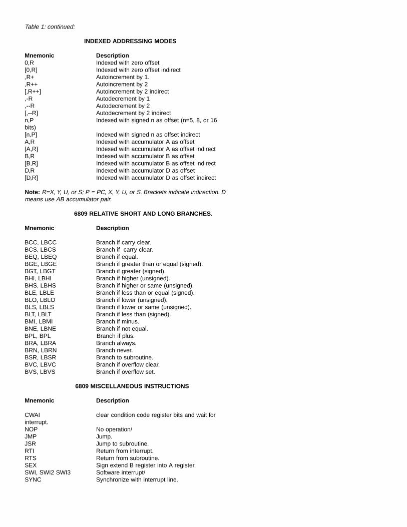
Table 1: continued:
INDEXED ADDRESSING MODES
Mnemonic Description0,R Indexed with zero offset[0,R] Indexed with zero offset indirect,R+ Autoincrement by 1.,R++ Autoincrement by 2[,R++] Autoincrement by 2 indirect,-R Autodecrement by 1,--R Autodecrement by 2[,--R] Autodecrement by 2 indirectn,P Indexed with signed n as offset (n=5, 8, or 16bits)[n,P] Indexed with signed n as offset indirectA,R Indexed with accumulator A as offset[A,R] Indexed with accumulator A as offset indirectB,R Indexed with accumulator B as offset[B,R] Indexed with accumulator B as offset indirectD,R Indexed with accumulator D as offset[D,R] Indexed with accumulator D as offset indirect
Note: R=X, Y, U, or S; P = PC, X, Y, U, or S. Brackets indicate indirection. Dmeans use AB accumulator pair.
6809 RELATIVE SHORT AND LONG BRANCHES.
Mnemonic Description
BCC, LBCC Branch if carry clear.BCS, LBCS Branch if carry clear.BEQ, LBEQ Branch if equal.BGE, LBGE Branch if greater than or equal (signed).BGT, LBGT Branch if greater (signed).BHI, LBHI Branch if higher (unsigned).BHS, LBHS Branch if higher or same (unsigned).BLE, LBLE Branch if less than or equal (signed).BLO, LBLO Branch if lower (unsigned).BLS, LBLS Branch if lower or same (unsigned).BLT, LBLT Branch if less than (signed).BMI, LBMI Branch if minus.BNE, LBNE Branch if not equal.BPL, BPL Branch if plus.BRA, LBRA Branch always.BRN, LBRN Branch never.BSR, LBSR Branch to subroutine.BVC, LBVC Branch if overflow clear.BVS, LBVS Branch if overflow set.
6809 MISCELLANEOUS INSTR UCTIONS
Mnemonic Description
CWAI clear condition code register bits and wait forinterrupt.NOP No operation/JMP Jump.JSR Jump to subroutine.RTI Return from interrupt.RTS Return from subroutine.SEX Sign extend B register into A register.SWI, SWI2 SWI3 Software interrupt/SYNC Synchronize with interrupt line.
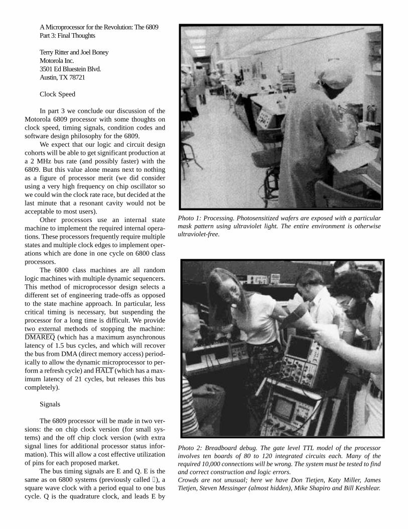
A Microprocessor for the Revolution: The 6809Part 3: Final Thoughts
Terry Ritter and Joel BoneyMotorola Inc.3501 Ed Bluestein Blvd.Austin, TX 78721
Clock Speed
In part 3 we conclude our discussion of theMotorola 6809 processor with some thoughts onclock speed, timing signals, condition codes andsoftware design philosophy for the 6809.
We expect that our logic and circuit designcohorts will be able to get significant production ata 2 MHz bus rate (and possibly faster) with the6809. But this value alone means next to nothingas a figure of processor merit (we did considerusing a very high frequency on chip oscillator sowe could win the clock rate race, but decided at thelast minute that a resonant cavity would not beacceptable to most users).
Other processors use an internal statemachine to implement the required internal opera-tions. These processors frequently require multiplestates and multiple clock edges to implement oper-ations which are done in one cycle on 6800 classprocessors.
The 6800 class machines are all randomlogic machines with multiple dynamic sequencers.This method of microprocessor design selects adifferent set of engineering trade-offs as opposedto the state machine approach. In particular, lesscritical timing is necessary, but suspending theprocessor for a long time is difficult. We providetwo external methods of stopping the machine:DMAREQ (which has a maximum asynchronouslatency of 1.5 bus cycles, and which will recoverthe bus from DMA(direct memory access) period-ically to allow the dynamic microprocessor to per-form a refresh cycle) and HALT (which has a max-imum latency of 21 cycles, but releases this buscompletely).
Signals
The 6809 processor will be made in two ver-sions: the on chip clock version (for small sys-tems) and the off chip clock version (with extrasignal lines for additional processor status infor-mation). This will allow a cost effective utilizationof pins for each proposed market.
The bus timing signals are E and Q. E is thesame as on 6800 systems (previously called ∅ ), asquare wave clock with a period equal to one buscycle. Q is the quadrature clock, and leads E by
Photo 1: Processing. Photosensitized wafers are exposed with a particularmask pattern using ultraviolet light. The entire environment is otherwiseultraviolet-free.
Photo 2: Breadboard debug. The gate level TTLmodel of the processorinvolves ten boards of 80 to 120 integrated circuits each. Many of therequired 10,000 connections will be wrong. The system must be tested to findand correct construction and logic errors.Crowds are not unusual; here we have Don Tietjen, Katy Miller, JamesTietjen, Steven Messinger (almost hidden), Mike Shapiro and Bill Keshlear.
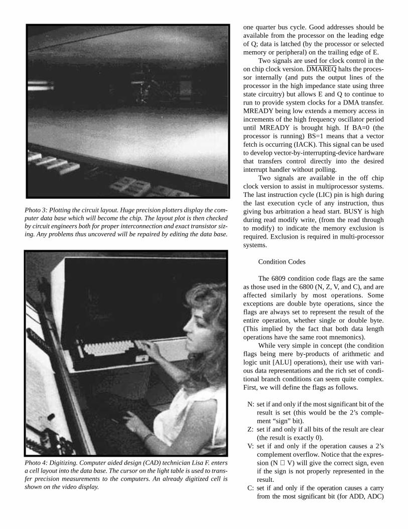
one quarter bus cycle. Good addresses should beavailable from the processor on the leading edgeof Q; data is latched (by the processor or selectedmemory or peripheral) on the trailing edge of E.
Two signals are used for clock control in theon chip clock version. DMAREQ halts the proces-sor internally (and puts the output lines of theprocessor in the high impedance state using threestate circuitry) but allows E and Q to continue torun to provide system clocks for a DMAtransfer.MREADY being low extends a memory access inincrements of the high frequency oscillator perioduntil MREADY is brought high. If BA=0 (theprocessor is running) BS=1 means that a vectorfetch is occurring (IACK). This signal can be usedto develop vector-by-interrupting-device hardwarethat transfers control directly into the desiredinterrupt handler without polling.
Two signals are available in the off chipclock version to assist in multiprocessor systems.The last instruction cycle (LIC) pin is high duringthe last execution cycle of any instruction, thusgiving bus arbitration a head start. BUSYis highduring read modify write, (from the read throughto modify) to indicate the memory exclusion isrequired. Exclusion is required in multi-processorsystems.
Condition Codes
The 6809 condition code flags are the sameas those used in the 6800 (N, Z, V, and C), and areaffected similarly by most operations. Someexceptions are double byte operations, since theflags are always set to represent the result of theentire operation, whether single or double byte.(This implied by the fact that both data lengthoperations have the same root mnemonics).
While very simple in concept (the conditionflags being mere by-products of arithmetic andlogic unit [ALU] operations), their use with vari-ous data representations and the rich set of condi-tional branch conditions can seem quite complex.First, we will define the flags as follows.
N: set if and only if the most significant bit of theresult is set (this would be the 2’s comple-ment “sign” bit).
Z: set if and only if all bits of the result are clear(the result is exactly 0).
V: set if and only if the operation causes a 2’scomplement overflow. Notice that the expres-sion (N ⊕ V) will give the correct sign, evenif the sign is not properly represented in theresult.
C: set if and only if the operation causes a carryfrom the most significant bit (for ADD, ADC)
Photo 4: Digitizing. Computer aided design (CAD) technician Lisa F. entersa cell layout into the data base. The cursor on the light table is used to trans-fer precision measurements to the computers. An already digitized cell isshown on the video display.
Photo 3: Plotting the circuit layout. Huge precision plotters display the com-puter data base which will become the chip. The layout plot is then checkedby circuit engineers both for proper interconnection and exact transistor siz-ing. Any problems thus uncovered will be repaired by editing the data base.
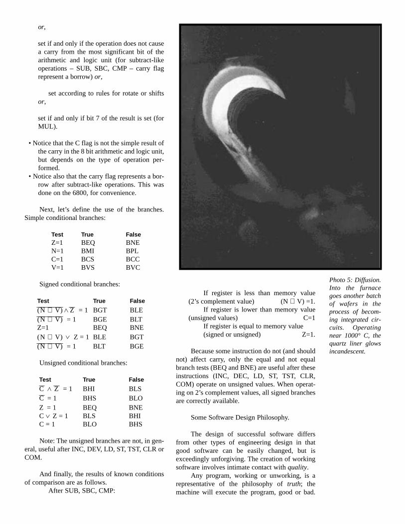
or,
set if and only if the operation does not causea carry from the most significant bit of thearithmetic and logic unit (for subtract-likeoperations – SUB, SBC, CMP– carry flagrepresent a borrow) or,
set according to rules for rotate or shiftsor,
set if and only if bit 7 of the result is set (forMUL).
• Notice that the C flag is not the simple result ofthe carry in the 8 bit arithmetic and logic unit,but depends on the type of operation per-formed.
• Notice also that the carry flag represents a bor-row after subtract-like operations. This wasdone on the 6800, for convenience.
Next, let’s define the use of the branches.Simple conditional branches:
Test True FalseZ=1 BEQ BNEN=1 BMI BPLC=1 BCS BCCV=1 BVS BVC
Signed conditional branches:
Test True False
(N ⊕ V) Z = 1 BGT BLE(N ⊕ V) = 1 BGE BLTZ=1 BEQ BNE(N ⊕ V) Z = 1 BLE BGT(N ⊕ V) = 1 BLT BGE
Unsigned conditional branches:
Test True False
C Z = 1 BHI BLSC = 1 BHS BLOZ = 1 BEQ BNEC Z = 1 BLS BHIC = 1 BLO BHS
Note: The unsigned branches are not, in gen-eral, useful after INC, DEV, LD, ST, TST, CLR orCOM.
And finally, the results of known conditionsof comparison are as follows.
After SUB, SBC, CMP:
If register is less than memory value (2’s complement value) (N ⊕ V) =1.
If register is lower than memory value(unsigned values) C=1
If register is equal to memory value(signed or unsigned) Z=1.
Because some instruction do not (and shouldnot) affect carry, only the equal and not equalbranch tests (BEQ and BNE) are useful after theseinstructions (INC, DEC, LD, ST, TST, CLR,COM) operate on unsigned values. When operat-ing on 2’s complement values, all signed branchesare correctly available.
Some Software Design Philosophy.
The design of successful software differsfrom other types of engineering design in thatgood software can be easily changed, but isexceedingly unforgiving. The creation of workingsoftware involves intimate contact with quality.
Any program, working or unworking, is arepresentative of the philosophy of truth; themachine will execute the program, good or bad.
Photo 5: Diffusion.Into the furnacegoes another batchof wafers in theprocess of becom-ing integrated cir-cuits. Operatingnear 1000° C, thequartz liner glowsincandescent.
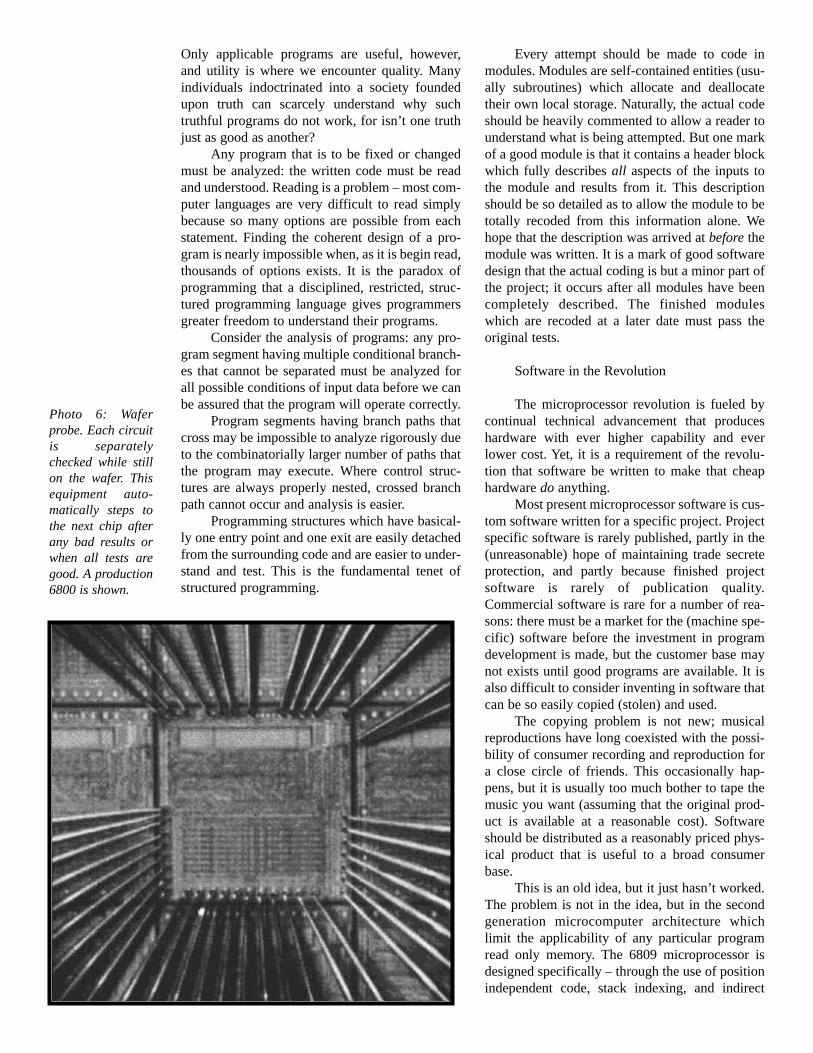
Only applicable programs are useful, however,and utility is where we encounter quality. Manyindividuals indoctrinated into a society foundedupon truth can scarcely understand why suchtruthful programs do not work, for isn’t one truthjust as good as another?
Any program that is to be fixed or changedmust be analyzed: the written code must be readand understood. Reading is a problem – most com-puter languages are very difficult to read simplybecause so many options are possible from eachstatement. Finding the coherent design of a pro-gram is nearly impossible when, as it is begin read,thousands of options exists. It is the paradox ofprogramming that a disciplined, restricted, struc-tured programming language gives programmersgreater freedom to understand their programs.
Consider the analysis of programs: any pro-gram segment having multiple conditional branch-es that cannot be separated must be analyzed forall possible conditions of input data before we canbe assured that the program will operate correctly.
Program segments having branch paths thatcross may be impossible to analyze rigorously dueto the combinatorially larger number of paths thatthe program may execute. Where control struc-tures are always properly nested, crossed branchpath cannot occur and analysis is easier.
Programming structures which have basical-ly one entry point and one exit are easily detachedfrom the surrounding code and are easier to under-stand and test. This is the fundamental tenet ofstructured programming.
Every attempt should be made to code inmodules. Modules are self-contained entities (usu-ally subroutines) which allocate and deallocatetheir own local storage. Naturally, the actual codeshould be heavily commented to allow a reader tounderstand what is being attempted. But one markof a good module is that it contains a header blockwhich fully describes all aspects of the inputs tothe module and results from it. This descriptionshould be so detailed as to allow the module to betotally recoded from this information alone. Wehope that the description was arrived at before themodule was written. It is a mark of good softwaredesign that the actual coding is but a minor part ofthe project; it occurs after all modules have beencompletely described. The finished moduleswhich are recoded at a later date must pass theoriginal tests.
Software in the Revolution
The microprocessor revolution is fueled bycontinual technical advancement that produceshardware with ever higher capability and everlower cost. Yet, it is a requirement of the revolu-tion that software be written to make that cheaphardware do anything.
Most present microprocessor software is cus-tom software written for a specific project. Projectspecific software is rarely published, partly in the(unreasonable) hope of maintaining trade secreteprotection, and partly because finished projectsoftware is rarely of publication quality.Commercial software is rare for a number of rea-sons: there must be a market for the (machine spe-cific) software before the investment in programdevelopment is made, but the customer base maynot exists until good programs are available. It isalso difficult to consider inventing in software thatcan be so easily copied (stolen) and used.
The copying problem is not new; musicalreproductions have long coexisted with the possi-bility of consumer recording and reproduction fora close circle of friends. This occasionally hap-pens, but it is usually too much bother to tape themusic you want (assuming that the original prod-uct is available at a reasonable cost). Softwareshould be distributed as a reasonably priced phys-ical product that is useful to a broad consumerbase.
This is an old idea, but it just hasn’t worked.The problem is not in the idea, but in the secondgeneration microcomputer architecture whichlimit the applicability of any particular programread only memory. The 6809 microprocessor isdesigned specifically – through the use of positionindependent code, stack indexing, and indirect
Photo 6: Waferprobe. Each circuitis separatelychecked while stillon the wafer. Thisequipment auto-matically steps tothe next chip afterany bad results orwhen all tests aregood. A production6800 is shown.
addressing – to allow the creation of standard pro-gram read only memories. This creates a marketopportunity for a brand new standard softwareindustry. We knew this when we included thesefeatures; you’re welcome, entrepreneurs!
Summary
We wrote this series of articles not only todisclose the 6809 but mainly to put down in printthe rational and reasoning behind the 6809. Itwould have benefited us if the designers of the6800 had documented their rationale. We wouldalso like to think we have stimulated some interestin the personal computing community for solu-tions to the software problem and for the study ofcomputer architecture. The big challenge forarchitects in the next decade and beyond will be todesign computers that can effectively utilize thehuge number of devices – 1,000,000 transistors by1985 – that semiconductor technology will be ableto put on one 25 mm2 piece of silicon.
No computer is designed in a vacume, andwe would like to thank all of our customers andthe people at Motorola who gave us valuableinput. Special thanks go to the dozens of people –two many to enumerate – who have been or arestill actively involved in the design, implementa-tion and production of the MC6809. Without theirindividual talents and dedication to what seemedto be impossible tasks and impossible schedules,the MC6809 could not have been realized.■