Texas Analog Center of Excellence - CVT-Dallas Analog Center of Excellence . Mission ... 2011...
34
Texas Analog Center of Excellence
Transcript of Texas Analog Center of Excellence - CVT-Dallas Analog Center of Excellence . Mission ... 2011...

Texas Analog Center of Excellence
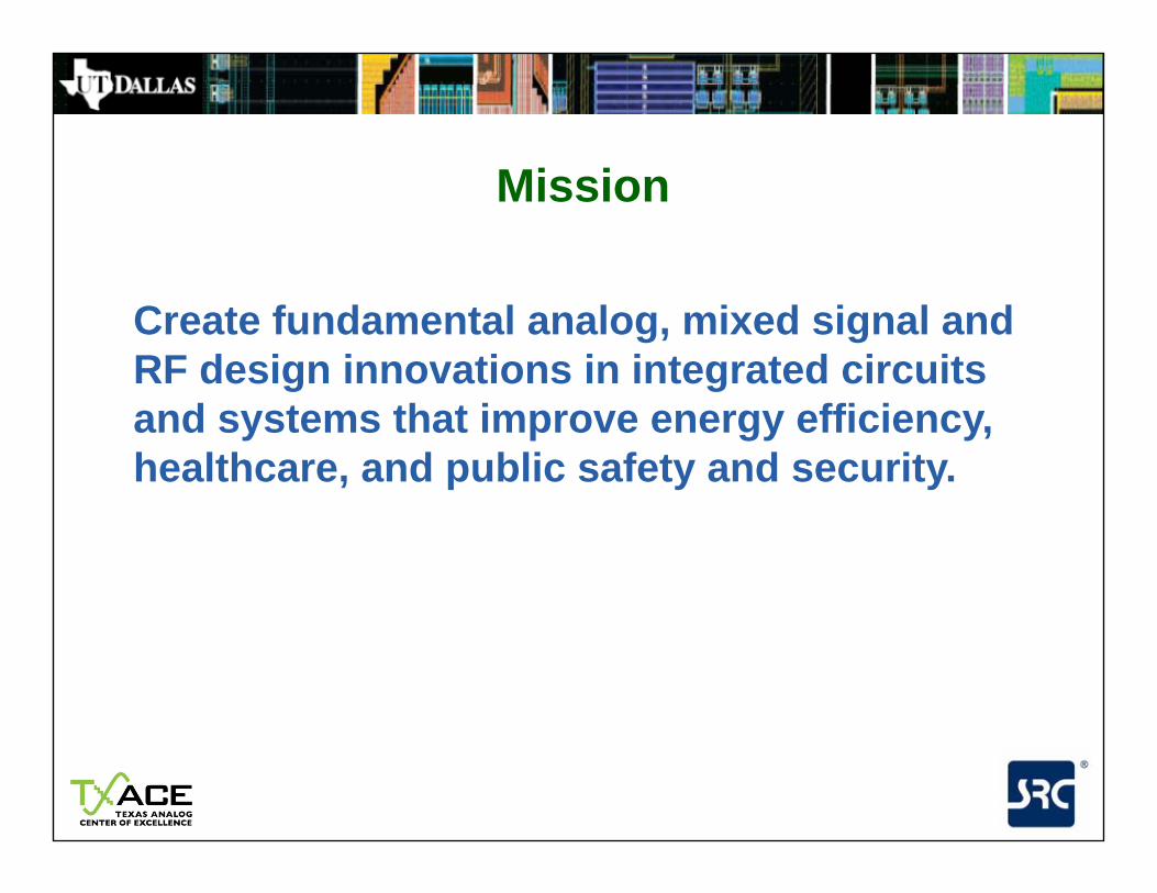
Mission
Create fundamental analog, mixed signal and RF design innovations in integrated circuits g gand systems that improve energy efficiency, healthcare, and public safety and security.

TI T ACE R h
SRC Industry Advisory Board
(AMD Freescale
TI TxACE Research Advisory Board
TxACE Executive Advisory Board
(SRC, TI, State of Texas, UT System,
(AMD, Freescale, GlobalFoundries,
IBM, Intel, TI)
UTD, Director)
Dean of ECS

TxACE SupportTxACE Support
• $1.5M/year from SRC• $600k/year of TI direct funding• $1.5M/year from the State of Texas• $900K/year of UTD and UT System funding• $900K/year of UTD and UT System funding• $4.5M endowment for chairs and professorships• $2M for TxACE laboratory renovation• Overall funding greater than $18 million for the first 3 years.

New Additions to UTD Analog Program g g
Prof. Yun Chiu: ADC Prof. Donsheng Ma: Prof. Mark Lee: THz Prof. Yiorgos Makris:
Integrated Power Electronics: Profs. H. Lee and D. Ma
and other Baseband Analog
Integrated Power Electronics
Electronics Analog Testing
Baseband Analog: Profs. Y. Chiu, J. Liu, W. NamgoongRF & THz: Profs. B. Banerjee, R. Henderson, M. Lee, K. OAnalog Testing: Prof. Y. MakrisThe largest and most comprehensive analog program in US.
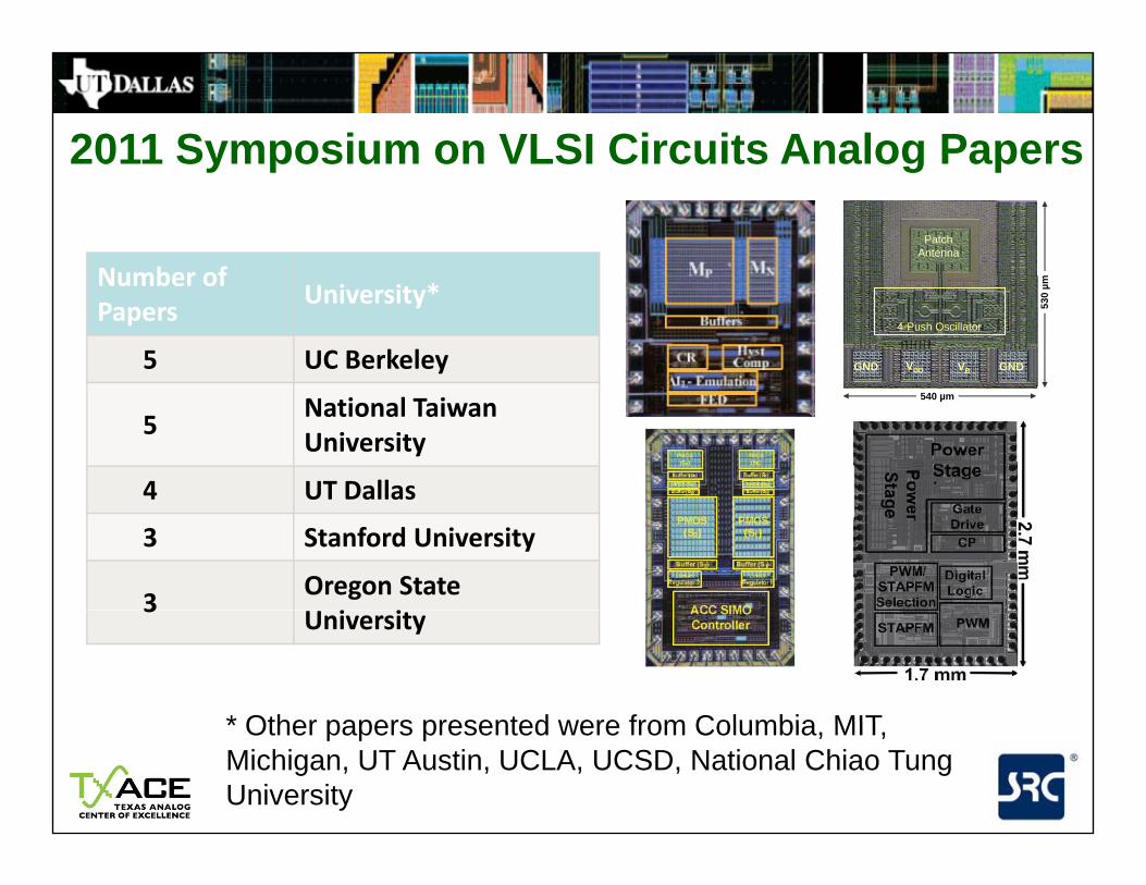
2011 Symposium on VLSI Circuits Analog Papers
Number of
2011 Symposium on VLSI Circuits Analog Papers
PatchAntenna
Number of Papers
University*
5 UC Berkeley VDD
4-Push Oscillator
GND GNDVB
530
µm
5National Taiwan University
4 UT Dallas
540 µm
4 UT Dallas
3 Stanford University
3Oregon State
i i3
University
* Other papers presented were from Columbia MIT* Other papers presented were from Columbia, MIT, Michigan, UT Austin, UCLA, UCSD, National Chiao Tung University

Fellowship Committee, Research Committee
Director: K. K. OResearch Committee, Space Committee
E ti C ittExecutive Committee (B. Floyd, D. Ma, Y. Chiu, D. Allstot, R. Harjani)
Analog Circuits and Techs. for Security and Safety (B. Floyd, N. Carolina State Univ )
Analog Circuits and Techs. for Health Care (R. Harjani, U. of Minnesota)
Analog Circuits and Techs. for Energy Efficiency (D. Ma, U. of Texas Dallas)Carolina State Univ.) Minnesota) Texas, Dallas)
Fundamental Analog Circuits Research (D Allstot U Washington)Fundamental Analog Circuits Research (D. Allstot, U. Washington)
• Improve research infrastructure • Increase interaction among researchersg
• Better focus research tasks• Better leverage the diverse capabilities of PI’s
• Define new research directions for consideration by IAB

TxACE TeamTxACE TeamOregon State
Washington
MinnesotaRPI MIT
Cornell U.U. Mass
UC BerkeleyIowa State Ohio State
YaleRPI
CMUStanford
Columbia
Arizona State
UC BerkeleyIllinois
ArkansasGeorgia Tech
NMSUNCSU
FloridaSeoul National U
NUI Maynooth
UNTTexas Tech
SMU
UT Austin
UT DallasTexas A&M
Georgia Tech
• 70 research tasks at 31 universities
NUI Maynooth
Cambridge
Rice
• 70 research tasks at 31 universities• Largest university based analog center in the
world.

TxACE TeamC ea
UNT • 36 tasks at 7 i iti iTexas Tech UT Dallas SMU
Texas A&M
universities in Texas.
• Enabled largelyRiceUT Austin • Enabled largely
by the state funding. g

TxACE Organization (68 PI’s and Co-PI’s)TxACE Organization, (68 PI s and Co PI s)Investigator Institution Investigator Institution Investigator Institution
David Allstot U Washington Arjang Hassibi UT-Austin Saraju Mohanty U North TX
U CaliforniaE. Alon U. California, Berkeley Mona Hella RPI Un-Ku Moon Oregon State U
A. Apsel Cornell U. Rashaunda Henderson UT-Dallas Boris Murmann Stanford U.
Bertan A i St t S b ti H T A&M U M kh dh G i T hBertan Bakkaloglu Arizona State Sebastian Hoyos Texas A&M U Mukhopadhyay Georgia Tech.
Poras Balsara UT-Dallas Roozbeh Jafari UT-Dallas Won Namgoong UT-Dallas
Bhaskar Banerjee UT-Dallas Aydin Ilker
Karsilayan Texas A&M U Ken O UT-Dallas
Leonidas Bieris UT-Dallas Sayfe Kiaei Arizona State Vojin Oklobdzija New Mexico State
Andrew Blanchard UT-Dallas Chris Kim U. Minnesota Sule Ozev Arizona State
Burleson U Mass Jaeha Kim Seoul Sam Palermo Texas A&M UBurleson U. Mass Jaeha Kim National U Sam Palermo Texas A&M U
Shawn Blanton Carnegie Mellon Peter Kinget Columbia Larry Pileggi Carnegie Mellon U
Joe Brewer U Florida Elias Kougianos U North Texas John Ringwood National U of Ireland Naymooth

TxACE Organization, (68 PI’s and Co-PI’s)C O ga at o , (68 s a d Co s)Investigator Institution Investigator Institution Investigator Institution
Abhijit Chatterjee Georgia Tech Farinaz Koushanfar Rice U Elyse Rosenbaum U Ill-Urbana-Champaign
Degang Chen Iowa State U Hoi Lee UT-Dallas Jaijeet Roychowdhury U Cal-Berkeley
Frank De Lucia Ohio State U Changzhi Li Texas Tech U Mohammad Saquib UT-Dallas
Donald Yu-Jia Di U. Arkansas, Feyat. Donald Yu-Chun Lie Texas Tech U Naresh Shanbhag U Ill-Urbana-Champaign
Kamran Entesari TAMU Peng Li Texas A&M U Michael Shur RPI
Brian L. Evans UT-Austin Xin Li Carnegie Mellon
Jose Silva-Martinez Texas A&M U
Terri Fiez Oregon State U Jin Liu UT-Dallas V. Stojanovic MIT
Brian Floyd NCSU Dongsheng Ma UT-Dallas Murat Torlak UT-Dallas
Randy Geiger Iowa State U H.A. Mantooth U Arkansas Eric Vogel UT-Dallas
R jit Gh UT A ti Yi M k i Y l U Xi Ch Zh RPIRanjit Gharpurey UT- Austin Yiorgos Makris Yale U Xi-Cheng Zhang RPI
Ping Gui Southern Methodist Jose Silva-Martinez TAMU Dian Zhou UT-Dallas
Ramesh Harjani U Minnesota Richard McMahon Cambridge UMcMahon
2011 VLSI Symposium on Circuits, 13 Analog Papers by TxACE PI’s. This is ~20-25% of all the analog papers at the Symposium.

TxACE Research Facility• Shared facility for characterization of circuits including those operating
at mm-wave and sub-mm-wave frequencies. • Network Analyses Noise and
y
• Network Analyses, Noise, and Linearity measurements up to 325 GHz. (Partnering with Agilent)Agilent)
• Selective measurements up to 850 GHz.
• Measurements up to multi THz using an FTIR.
• Antenna measurement up to 325• Antenna measurement up to 325 GHz.
• TxACE members have access.~8000 ft2. 50 cubicles for researchers.
• Top electronic circuits characterization laboratory in US.

Safety and Security (Millimeter-Wave)Brian Floyd, NCSU
• Millimeter wave circuits• 77-81-GHz radar circuits with built-in
self test• 180-300 GHz spectrometer• Antennas for radars andAntennas for radars and
spectrometer• Beam forming arrays• Techniques to reduce the number of• Techniques to reduce the number of
pixels in “Superman” imagers• Frequency channelized ADC
S b TH t itt t• Sub-THz transmitter components• Mixed-signal architecture for low-power
physical unclonable functions

77-81 GHz Automotive Radar
• Warning drivers of impending unsafe conditions can save more than• Warning drivers of impending unsafe conditions can save more than 1,000,000 lives per year world wide.
• Cost of automobile accidents is $160B/year to US economy.Radar stands for radio detection and ranging• Radar stands for radio detection and ranging.
• Radar transmits, and receives and analyzes reflected signals to detect and determine the shape, size, make-up, position, and velocity of the object that reflected the transmitted signalobject that reflected the transmitted signal.
• The cost of 77-GHz III-V integrated circuits (IC’s) has been identified as a key problem. More than 10 radars per ehicle 100 million ehicles sold in 2007
14
• More than 10 radars per vehicle. ~100 million vehicles sold in 2007.• Many more consumer and industrial applications for radars.

Tunable RF and mm-wave voltage gmeasurements for BIST & healing (K. O, UTD)
Tunable Mixer Receiver Chain77-81 GHz • Key blocks of tunable
RF system• Measure and
CalibrateTunable IF Amp
LO1~64 GHz
Detector
LNA
RF system• Tunable elements
• On-chip low loading self-detection
Calibrate• Power gain
• Frequency response
RF SystemVCO
Tunable
T/RSwitch
/4 LO2
FrequencySynthesizer
~16 GHz
detection
• Feedback control loop
response
• Linearity
tunable elements
Tunable
Tunable
77-81 GHz
y
IF AmpPower AmplifierTunable filter
DAC DAC
low noise
diode power
detector• Outputs of detectors are sampled using an ADC
Transmitter ChainMixer
: Schottky Barrier Diode Power Detector
ADC Digital Processing
low-noise amplifier
using an ADC• Digital data are processed• DACs are used to tune the tunable
elements 15

Integration of Millimeter Wave Antennas Using g gSystem in Package Techniques (R. Henderson, UTD)
1 mm CPW
Technology w (m) h (m) Atten. @ 60GHz (dB/mm)
Design 1 on FR408 50- line
4 82 i t i / i
RT/duroid 90 15 0.07GaAs 120 40 0.09CMOS
w/o p+well9.5 4 1.0
4.82 mm microstrip w/via CMOSw/ BCB
60 8 0.96
FR408 135 40 0.13
• FR408 has excellent characteristics at 60 GHz Costs 15X• FR408 has excellent characteristics at 60 GHz. Costs ~15X lower than duroid.
• Good agreement between simulations and measurements.

280-GHz Schottky Diode Detector (K. O, UTD)• Integrates on-chip
patch antennasIntegrates differential
y ( , )
• Integrates differential amplifier following the PGS Schottky diode d t tdetector
• 2x2 Array• 130-nm CMOS
R. Han et al., “280-GHz Schottky Diode Detector in 130-nm Digital CMOS,” 2010 Custom Integrated Circuits Conference.

280-GHz Schottky Diode Detector (K. O, UTD)80 G Sc ott y ode etecto ( O, U )
• 290-GHz transmitted power from the source is 4mW and modulation frequency of 250Hz.
• Should work with less than 1W when properly designed.

280-GHz Schottky Diode Detector (K. O, UTD)y ( , )
• Diode cut-off frequency is ~2 THz. A 1-THz detector should be possible.

MIMO Radar for Pixel Reduction in MM-Wave Imaging (M. Saquib, UTD)
(left) Original target; (right) Traditional radar image with 16 antennas. Here number of transmit antennas (M) = 1 and number of receive antennas (N) = 15.
(left) MIMO radar image with 11 antennas. Here M=3 and N=8; (right) MIMO radar image with 7 antennas
• Minimum mean square error (MMSE) receiver with reduced
MIMO radar image with 7 antennas. Here M=2 and N=5 and STBC is employed with MMSE like receiver.
Minimum mean square error (MMSE) receiver with reduced complexity and space-time block code (STBC) technique in a MIMO radar imaging system.
• Capable of providing the same image resolution as the traditional p p g gone but with almost 60% fewer antennas.

180-300 GHz Spectrometerp
F. Patten, MACS P
• Rotational spectroscopy.
Proposer Day Conf., Darpa, N 2005
p py• Specificity in the
presence a large n mber ofNov. 2005 number of molecule types in a mixture.
• Detect down to PPT.
Signal generator180 300 GH
Receiver180-300 GHz
Folded Absorption Cell, 30 cm180-300 GHz 180-300 GHz

Some of Molecules on the EPA ListGas Frequency (MHz) Fatality
Limit Gas Frequency (MHz) Fatality Limit
Hydrogen Cyanide (HCN) 265887.1094 15-50
ppm/hr Methyl Bromide (CH3Br) 267801.2188
Cyanogen Chloride (ClCN) 267199.53125 Ethylene Oxide (C2H4O) 263292.5156 200
ppm/hr
Cyanogen Bromide (BrCN) 263578.3438 Acrolein (C3H4O) 267279.3594 1.4 ppm/hr
Acetonitrile (CH3CN) 239096.6719 Propionitrile (C2H5CN) 268829.0625
Carbonyl Sulfide (OCS) 267530.4219 Vinyl Chloride (C2H3Cl) 266151.2969
Methyl Chloride (CH3Cl) 265785.4219 Methyl mercaptan (CH SH) 227564.6719 23 ppm/hr(CH3SH)
Acrylonitrile (C2H3CN) 265935.2031 Methyl isocyanate (CH3NCO) 269788.6094 5 ppm/hr
Dichloromethane (CH2Cl2)
259215.3906 Methanol (CH3OH) 250507.1563( 2 2)
Methyl Iodide (CH3I) 269864.9063 Formaldehyde 211211 100 ppb
CO (230538), Ethanol (246663.6), Acetone (259618.4), NO (267199.53125)
• Detection of ethanol in a car.• Monitor leaks of various fluids in vehicles.

553-GHz Signal Generation (K. O, UTD)
150
200
250
552.8 GHz
[nW
]
VDD = 1.4 V
4f0 Fixed Mirror
MovableMirror
Beam Splitter
fOSC
sity OSCf
cλ
On-chipPatch
AntennaM
ichelsonInterferoem
eter
4-PushOscillator
0
50
100
5f0
2f0 3f0f0
PR
AD[
6f0
IBIAS = 46 mABolometerFFT
ffOSC
2λ
Inte
ns
138.
2 G
Hz
276.
4 G
Hz
414.
6 G
Hz
691.
0 G
Hz
829.
2 G
Hz
• Quadruple-push using 150-GHz quadrature oscillators for frequency quadrupling.
0100 300 500 700 900
Frequency [GHz]
frequency quadrupling.• Current mode phase combining.• On-chip antenna for quasi-optical measurements.• Fabricated in 45-nm CMOS with low leakage transistors.
P k t 553 GH
PatchAntenna
30
m
• Peak at 553 GHz. • 5th and 6th harmonics at 691 and 829.2 GHz.• Compared to the previously reported 410-GHz signal
generation circuit using a push-push oscillator, output power d f 4X hi h d 1 5X hi h
VDD
4-Push Oscillator
GND GNDVB
5
and frequency are 4X higher and ~1.5X higher. 540 m
These are fundamental technologies that can easily be applied to mm-wave and sub-mm wave communication circuits.

Health Care (Non-invasive Diagnostics)( g )Ramesh Harjani, U. of Minnesota• Ultrasound
• Adaptive data prediction based ltraso nd recei erultrasound receiver
• Ultrasound power amplifier• Template based wake up circuits for low
bipower bio-sensors.• Millimeter wave imaging• Spectrometer for breath analyses• Low power analog front-end IC for
implantable cardioverter defibrillator devices• Photovoltaic (PV) power harvesting for
i l t bl d iimplantable devices.

Health Care (Non-invasive Diagnostics)Health Care (Non invasive Diagnostics)Ramesh Harjani, U. of Minnesota
Bio molec le sensors (Lab on a Chip)• Bio-molecule sensors (Lab on a Chip)• Nano-wire sensing• Analog signal processing in human cells• Microwave-Based Label-Free DNA
Sensing

Photovoltaic (PV) Power Harvesting CMOS ICs ( ) g(Hassibi, UT, Austin)
Implantable
hvPhoton Flux (hv)
PolarizingElectric Field
Photon Flux (hv)Polarizing
Electric FieldState of Art: I l t d d i MRI i tibl d Implantable
ChipImplanted devices use MRI-incompatible and coils or antennas for “wireless” power deliveryObjectives: Use optical means to deliver power through the ti t i l t d d i (0 7 1 )
0.5 mm
CMOS Chip tissue to an implanted device (0.7- 1 m )Novelty: Use on-chip diode as CMOS-compatible energy harvesting elements
Accomplishments• Designed and successfully tested P+/Nwell PV cells
in 0.18µm bulk CMOS. (No process modifications) General concept and the chip
micrograph of a CMOS implanted de ice
PVCells
SensorCircuit
PolarizedElectrodes
Off-chipTransducer
µ ( p )• Demonstrated on-chip 100nW ring oscillator-based
sensors that use the CMOS PV cells (2mm x 2 mm) as their energy source.
• Designed and successfully tested in vitro a PV driven
device
• Designed and successfully tested in-vitro a PV-driven CMOS implanted sensor.

Energy Efficiency, Dong-Sheng Ma, UTD• Single inductor multiple output
power converters
gy y, g g ,
High V lt• LED driver
• Transistor sizing for energy efficiency
Voltage
• System level models and design of power delivery networks with on-chip voltage regulators
Low Votage
Medium Voltage
• Power efficient power-line communications for enabling smart grid applications
• Optimum control of power converters for improved efficiency

Energy Efficiency, Dong-Sheng Ma, UTDEnergy Efficiency, Dong Sheng Ma, UTD• Energy harvesting circuits (thermal, light,
multiple source and dc-dc converter) Ph t lt i (PV) h ti• Photovoltaic (PV) power harvesting CMOS ICs (W/mm2)
• Single-Inductor multiple-input multiple-t t i t t d DC DC toutput integrated DC-DC converter
• Reduction of sensors in electronic systems for wind turbines

Fast Transient Switching Converter for DVS (D. Ma, UTD)
• Hysteric control loop with iL emulation circuitsHysteric control loop with iL emulation circuits.• Charge recycling controller.• Charge recycling reduces the dynamic voltage
scaling (DVS) down tracking speed from 130S/Vscaling (DVS) down tracking speed from 130S/V to 14S/V.
• 400 mA load transient, recovery times of 8 and 14 S are achieved with 35 and 52 mV undershootS are achieved with 35 and 52 mV undershoot and overshoot voltages

Fundamental Analog Circuits Research
• Baseband analog electronics• High sampling rate ADC’s: Energy efficient 10-20 GS/s ADC, Frequency
gDavid Allstot, U. of Washington
g p g gy , q ychannelized ADC.
• Other ADC’s: ADC’s for broadband applications, Low complexity ADC.• High speed I/O: MIMO for wire line Comm., Digitally enhanced I/O, Sub-g p , g y ,
1mW/Gbps Serial I/O transceiver, Variation tolerant calibration circuit.• Sub-0.5V high accuracy CMOS temperature sensor
• RF and wireless • Reconfigurable antenna interface for low power wireless sensor nodes.• Wideband receiver
• TestingTesting• Low cost testing for > 50-GHz circuits. • Adaptive test for test cost reduction• Fault models for analog circuits• Fault models for analog circuits• Analyses of parametric measurements

Fundamental Analog Circuits Research
• 3D Integrated Heterogeneous systems (TSV’s)• CAD for mixed signal and RF/Millimeter wave simulations
gDavid Allstot, U. of Washington
g• Parallel simulations • Fast PVT tolerant design and simulation techniques• Multiple time scale simulations• Multiple time scale simulations
• Variability enabled nonlinear phase model for fast PLL simulationsHi hi l d l h ki f ti l• Hierarchical model checking for practical analog/mixed-signal design verification.
• Behavioral model generation algorithms

A/D Converter Synthesized with a Digital Flow (U.-K.
• Flash ADC is synthesized using standard digital library.• Comparators (2047) are implemented by cross coupling 2 3-input NAND
y g (Moon, Oregon State University)
Comparators (2047) are implemented by cross coupling 2 3 input NAND gates.
• Output data are linearized using the inverse function of Gaussian CDF.• Achieves 5 5 ENOB for 1 MHz input at 210 MSPS and 35 mWAchieves 5.5 ENOB for 1 MHz input at 210 MSPS and 35 mW.• 90-nm CMOS.
4042
SNDR
3234363840
nd S
FDR
[dB
]
SFDR
0 20 40 60 80 100 12026
283032
SND
R a
n
Input Frequency [MHz]

• The center is starting its third year.• Strong team.g• Excellent portfolio of research.• Working to improve research infrastructureWorking to improve research infrastructure
• TxACE space is fully functional.• Prof Y Chiu has been leading the effort to• Prof. Y. Chiu has been leading the effort to
alleviate the fabrication problems.• Starting to make noticeable impact to the Analog• Starting to make noticeable impact to the Analog
community.

Please register now for this complimentary symposium at https://alumni utdallas edu/Nhttps://alumni.utdallas.edu/NetCommunity/SSLPage.aspx?pid=509&frcrld=1