Realization of basic memory elements by bicmos logic and comparative study with cmos logic
Terahertz Imaging with CMOS/BiCMOS ProcessTechnologies
Ullrich R. Pfeiffer and Erik Öjefors
High-Frequency and Communication Technology, University of WuppertalRainer-Gruenter-Str. 21, D-42119 Wuppertal, Germany
Email: [email protected] and [email protected]
Abstract— Contrary to the common belief, silicon devices mayvery well operate beyond their cut-off frequency. The pushtowards terahertz frequencies, though, presents both challengesand opportunities for emerging applications. This paper sum-marizes recent attempts to use foundry-level silicon processtechnologies for the realization of terahertz electronic systems.
I. INTRODUCTION
Historically, terahertz radiation was generated by opticalmeans with the help of femto-second laser pulses and wasprimarily used for spectroscopic purposes in the scientificcommunity [1]. This band, which is defined by the sub-mmWave band from 300 GHz through 3 THz, is often referredto as the THz gap, loosely describing the lack of adequate tech-nologies to effectively bridge this transition region betweenmicrowaves and optics. The use of either electronic or photonictechniques has led to the subdivison in THz Electronic andTHz Photonic bands with frequencies spanning from 100 GHzthrough 10 THz as illustrated in Fig 1.
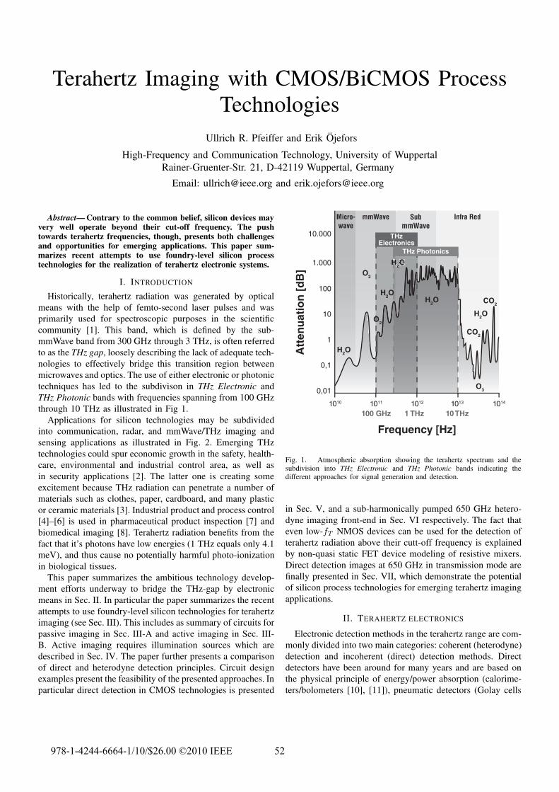
Applications for silicon technologies may be subdividedinto communication, radar, and mmWave/THz imaging andsensing applications as illustrated in Fig. 2. Emerging THztechnologies could spur economic growth in the safety, health-care, environmental and industrial control area, as well asin security applications [2]. The latter one is creating someexcitement because THz radiation can penetrate a number ofmaterials such as clothes, paper, cardboard, and many plasticor ceramic materials [3]. Industrial product and process control[4]–[6] is used in pharmaceutical product inspection [7] andbiomedical imaging [8]. Terahertz radiation benefits from thefact that it’s photons have low energies (1 THz equals only 4.1meV), and thus cause no potentially harmful photo-ionizationin biological tissues.
This paper summarizes the ambitious technology develop-ment efforts underway to bridge the THz-gap by electronicmeans in Sec. II. In particular the paper summarizes the recentattempts to use foundry-level silicon technologies for terahertzimaging (see Sec. III). This includes as summary of circuits forpassive imaging in Sec. III-A and active imaging in Sec. III-B. Active imaging requires illumination sources which aredescribed in Sec. IV. The paper further presents a comparisonof direct and heterodyne detection principles. Circuit designexamples present the feasibility of the presented approaches. Inparticular direct detection in CMOS technologies is presented
1010 1011 1012 1013 1014
Frequency [Hz]
O2
H2O
H2O
CO2
CO2
O3
100 GHz 1 THz 10 THz
Micro-
wave
Infra RedmmWave Sub
mmWave
H2O
]B
d[ n
o ita
un
ettA
0,01
0,1
1
10
100
1.000
10.000 THzElectronics
THz Photonics
H2O
H2O
O2
Fig. 1. Atmospheric absorption showing the terahertz spectrum and thesubdivision into THz Electronic and THz Photonic bands indicating thedifferent approaches for signal generation and detection.
in Sec. V, and a sub-harmonically pumped 650 GHz hetero-dyne imaging front-end in Sec. VI respectively. The fact thateven low-fT NMOS devices can be used for the detection ofterahertz radiation above their cutt-off frequency is explainedby non-quasi static FET device modeling of resistive mixers.Direct detection images at 650 GHz in transmission mode arefinally presented in Sec. VII, which demonstrate the potentialof silicon process technologies for emerging terahertz imagingapplications.
II. TERAHERTZ ELECTRONICS
Electronic detection methods in the terahertz range are com-monly divided into two main categories: coherent (heterodyne)detection and incoherent (direct) detection methods. Directdetectors have been around for many years and are based onthe physical principle of energy/power absorption (calorime-ters/bolometers [10], [11]), pneumatic detectors (Golay cells
978-1-4244-6664-1/10/$26.00 ©2010 IEEE 52
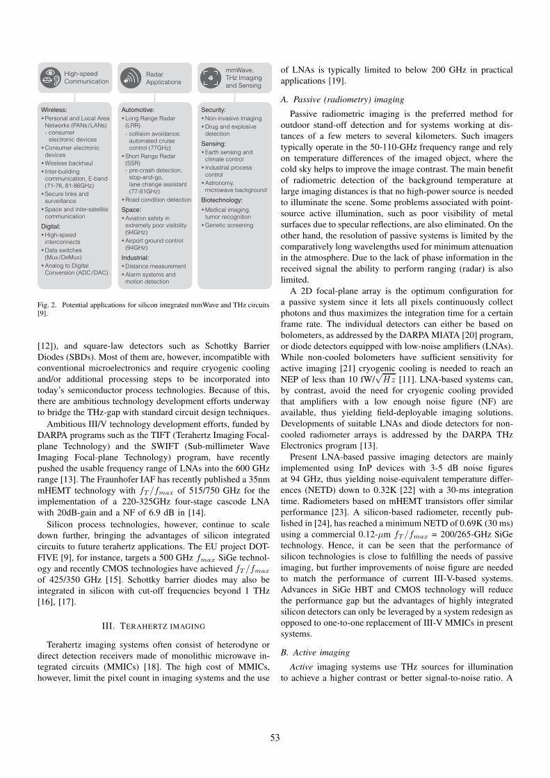
Fig. 2. Potential applications for silicon integrated mmWave and THz circuits[9].
[12]), and square-law detectors such as Schottky BarrierDiodes (SBDs). Most of them are, however, incompatible withconventional microelectronics and require cryogenic coolingand/or additional processing steps to be incorporated intotoday’s semiconductor process technologies. Because of this,there are ambitious technology development efforts underwayto bridge the THz-gap with standard circuit design techniques.
Ambitious III/V technology development efforts, funded byDARPA programs such as the TIFT (Terahertz Imaging Focal-plane Technology) and the SWIFT (Sub-millimeter WaveImaging Focal-plane Technology) program, have recentlypushed the usable frequency range of LNAs into the 600 GHzrange [13]. The Fraunhofer IAF has recently published a 35nmmHEMT technology with fT /fmax of 515/750 GHz for theimplementation of a 220-325GHz four-stage cascode LNAwith 20dB-gain and a NF of 6.9 dB in [14].
Silicon process technologies, however, continue to scaledown further, bringing the advantages of silicon integratedcircuits to future terahertz applications. The EU project DOT-FIVE [9], for instance, targets a 500 GHz fmax SiGe technol-ogy and recently CMOS technologies have achieved fT /fmax
of 425/350 GHz [15]. Schottky barrier diodes may also beintegrated in silicon with cut-off frequencies beyond 1 THz[16], [17].
III. TERAHERTZ IMAGING
Terahertz imaging systems often consist of heterodyne ordirect detection receivers made of monolithic microwave in-tegrated circuits (MMICs) [18]. The high cost of MMICs,however, limit the pixel count in imaging systems and the use
of LNAs is typically limited to below 200 GHz in practicalapplications [19].
A. Passive (radiometry) imaging
Passive radiometric imaging is the preferred method foroutdoor stand-off detection and for systems working at dis-tances of a few meters to several kilometers. Such imagerstypically operate in the 50-110-GHz frequency range and relyon temperature differences of the imaged object, where thecold sky helps to improve the image contrast. The main benefitof radiometric detection of the background temperature atlarge imaging distances is that no high-power source is neededto illuminate the scene. Some problems associated with point-source active illumination, such as poor visibility of metalsurfaces due to specular reflections, are also eliminated. On theother hand, the resolution of passive systems is limited by thecomparatively long wavelengths used for minimum attenuationin the atmosphere. Due to the lack of phase information in thereceived signal the ability to perform ranging (radar) is alsolimited.
A 2D focal-plane array is the optimum configuration fora passive system since it lets all pixels continuously collectphotons and thus maximizes the integration time for a certainframe rate. The individual detectors can either be based onbolometers, as addressed by the DARPA MIATA [20] program,or diode detectors equipped with low-noise amplifiers (LNAs).While non-cooled bolometers have sufficient sensitivity foractive imaging [21] cryogenic cooling is needed to reach anNEP of less than 10 fW/
√Hz [11]. LNA-based systems can,
by contrast, avoid the need for cryogenic cooling providedthat amplifiers with a low enough noise figure (NF) areavailable, thus yielding field-deployable imaging solutions.Developments of suitable LNAs and diode detectors for non-cooled radiometer arrays is addressed by the DARPA THzElectronics program [13].
Present LNA-based passive imaging detectors are mainlyimplemented using InP devices with 3-5 dB noise figuresat 94 GHz, thus yielding noise-equivalent temperature differ-ences (NETD) down to 0.32K [22] with a 30-ms integrationtime. Radiometers based on mHEMT transistors offer similarperformance [23]. A silicon-based radiometer, recently pub-lished in [24], has reached a minimum NETD of 0.69K (30 ms)using a commercial 0.12-µm fT /fmax = 200/265-GHz SiGetechnology. Hence, it can be seen that the performance ofsilicon technologies is close to fulfilling the needs of passiveimaging, but further improvements of noise figure are neededto match the performance of current III-V-based systems.Advances in SiGe HBT and CMOS technology will reducethe performance gap but the advantages of highly integratedsilicon detectors can only be leveraged by a system redesign asopposed to one-to-one replacement of III-V MMICs in presentsystems.
B. Active imaging
Active imaging systems use THz sources for illuminationto achieve a higher contrast or better signal-to-noise ratio. A
53

fast frequency agility may also provide spectroscopic identi-fication of materials. Active imaging distinguishes itself frompassive (radiometry) imaging, because one often detects theradiation as electric-field amplitude and phase similar to radarapplications. This enables imaging with three-dimensional andtomographical content which enhances the object detectioncapabilities [25], [26]. Active imaging sensors are defined inone of two ways, depending on whether the system uses (i)direct detectors as receivers where the sensitivity is defined asNEP and integration bandwidth, or (ii), heterodyne receiverswhere the sensitivity is determined by the noise figure andintegrated bandwidth. See Fig. 3 for an illustration of thedifferent receiver approaches.
a) Active Direct Detection
b) Active Heterodyne Detection
LNA∫
RF Detector
Video Amp
τ = 1/fps
Psig
LNA∫
τ = 1/fps
Psig Mixer IF Amp
SNR0 =Psig
NEP√
fps
SNR0 =Psig
kBTFfps
Fig. 3. Active imaging receivers. A direct detection receiver is shown infigure a), whereas figure b) shows a heterodyne receiver.
The overall system specification of an active imaging systemdepends greatly on the application requirements such as theimaging mode (transmission or reflection), the required spacialresolution, and the expected sensitivity. For the purpose of de-tector comparison, direct and heterodyne receiver architecturesmay be analyzed for a fixed video rate (e.g. 25 fps) and a fixedreceived power level (e.g. Psig = −50 dBm, 10 nW) at theantenna port. The video rate sets a limit on the maximumavailable integration time per pixel (τ = 1/fps).
For a given video rate (fps), the SNR0 for active directdetection can be written as,
SNR0 =Psig
NEP√
fps, (1)
where the noise-equivalent power (NEP) is defined as thepower at which the signal-to-noise ratio SNR0 is unity fora detector time constant of τ = 1 s. For active heterodynedetection the SNR0 can be written as
SNR0 =Psig
kBTFfps, (2)
where F is the noise factor and kBT is the thermal noisepower at temperature T .
The results of Eqn. 1 and 2 is shown in Fig. 4. The figureshows the direct detection NEP and heterodyne NF versus the
0 20 40 60 80 100
100
101
102
SNR0 [dB]
NE
P [
pW
/sq
rt(H
z)]
Psig
=10nW @25fps
0 20 40 60 80 1000
20
40
60
80
100
NF
[d
B]
HeterodyneDire
ct
Fig. 4. Comparison of direct detection and heterodyne receiver performancefor active imaging applications. To obtain images with a 20-dB SNR0 forinstance, one requires a system NEP of 20 pW/
√Hz in direct detection, but
a heterodyne receiver NF of only 90 dB. The comparison at room temperatureis based on a 25-fps video rate with Psig = 10 nW at the receiver pixel.
imaging SNR0. For a 20-dB SNR0 for instance, one requiresa system NEP of 20 pW/
√Hz in direct detection, but a
heterodyne receiver NF of only 90 dB. Note, the comparisonis done for detection at room temperature with a 25-fps videorate and a Psig = 10 nW at the receiver pixel. The detailsof the imaging setup, such as the physical FPA size, numberof pixels, total transmit power, and the path loss may lowerthe received pixel power Psig , but the lower received poweraffects both detection schemes equally.
This analysis clearly shows the superior performance ofheterodyne detection in active imaging applications, becausenoise figures may be as low as 42 dB in silicon at 650 GHz aswill be shown later in Sec. VI. However, implementation issuessuch as limitations of the LO drive power, the LO distribution,and the total DC power consumption limit the number ofheterodyne pixels in practical applications. The CMOS directdetectors presented in Sec. V with NEPs as low as 50 pW/
√Hz
at 650 GHz, therefore, present an attractive alternative whicheasily can support large arrays with 20.000 pixels.
IV. SUBMILLIMETER SOURCES IN SILICON FOR
TERAHERTZ IMAGING
At lower mmWave frequencies, where silicon devices stillexhibit power gain, amplifiers suffer from their low break-down voltages. High-performance SiGe HBTs exhibit break-down voltages of BVceo = 1.5 V and BVcbo = 4.5 V [9],while RF CMOS suffers from low drain voltages of about1 V in 65 nm technologies [27]. At lower mmWave frequen-cies, state-of-the-art SiGe power amplifiers have demonstratedsaturated output powers as high as 20 dBm at 60 GHz [28]and recently up to 8 dBm at 160 GHz in [29]. Submillime-ter sources for terahertz imaging, however, need to operatetransistors close to, or even above, their cutoff frequencies.Because of this, silicon based submillimeter wave sources have
54
only demonstrated comparatively low output power in the past.Power generation techniques beyond the cutoff frequency aredone in one of two ways, (i) directly extracted from oscillators,or (ii), up-converted from lower frequencies by the help offrequency multiplier chains.
Output Power of Silicon Technologies
Output Power [dBm]
-50
-40
-30
-20
-10
0
10
20
30
Frequency [GHz]0 100 200 300 400 500
Fig. 5. Published submillimeter sources in silicon. The figure shows saturatedoutput power versus operation frequency.
Recent publications have demonstrated silicon-based VCOsat 278-GHz with -38 dBm in [30] and -47 dBm at 410 GHzin 45-nm CMOS in [31], respectively. Linear superpositiontechniques in CMOS have been demonstrated up to -46 dBmat 324 GHz [32]. More applicable power levels for ac-tive imaging have recently been published in [33], where a325-GHz x18 frequency multiplier achieves up to -8 dBm. Themonolithic multiplier is implemented in an fmax-optimizedevaluation SiGe HBT technology [9] using cascaded transistor-based multiplication and amplification stages. This result com-pares quite well with III/V-based mHEMT multiplier chainspublished in [34], [34] and demonstrates the capability ofsilicon technologies for active illumination up to 325 GHz.A summary of integrated submillimeter sources in silicon isshown in Fig. 5 and Table I.
Fig. 6 shows the chip micrograph of the 325 GHz frequencymultiplier chain. The die size is 2.2×0.43-mm2. The circuitconsists of a 325-GHz doubler circuit fed differentially by twocascaded triplers. Each tripler is equipped with a frequencyselective power amplifier at the output in order to boostthe power entering the next multiplier stage and to suppressspurious frequencies. A differential amplifier is used at theinput to convert a 18-GHz single-ended signal from an off-chip synthesizer.
V. DIRECT DETECTION RECEIVER IN CMOS/SIGE
Unlike heterodyne detection, incoherent (direct) detectionfavors multi-pixel applications such as focal-plane arrays,where the power consumption per pixel should be minimalto enable large pixel counts. Direct detectors may consistof square-law detectors implemented in either bipolar or
DC−Bias 18GHz Input
Doubler
325GHz Output
325GHzTripler54GHz
PA54GHz
Tripler162GHzDiff.
Conv.162GHzPA
Fig. 6. Micrograph of a 325 GHz SiGe frequency multiplier chain with upto -8 dBm at 325 GHz [33].
CMOS technologies. A 600-GHz focal-plane arrays based ona differential NPN pair were first published in [36] and basedon resistive mixers in [37] respectively. The high frequencynoise in an SiGe HBT is dominated by the shot noise at thejunctions as well as the thermal noise in the intrinsic base andemitter resistances [38]. The noise of non-biased (cold) FETtransistor, however, are only limited by the thermal noise ofthe channel conductance and have demonstrated NEPs as lowas 50 pW/
√Hz at 650 GHz in a 65-nm CMOS SOI technology
[39].This performance compares well with conventional detec-
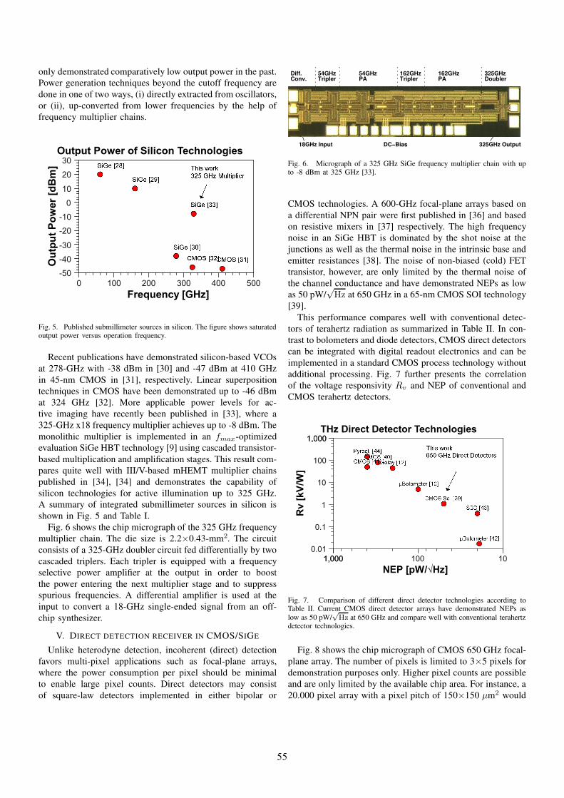
tors of terahertz radiation as summarized in Table II. In con-trast to bolometers and diode detectors, CMOS direct detectorscan be integrated with digital readout electronics and can beimplemented in a standard CMOS process technology withoutadditional processing. Fig. 7 further presents the correlationof the voltage responsivity Rv and NEP of conventional andCMOS terahertz detectors.
THz Direct Detector Technologies
µBolometer [42]
Rv [kV/W]
0.01
0.1
1
10
100
1,0001,000
NEP [pW/√Hz]1,0001,000 100 10
Fig. 7. Comparison of different direct detector technologies according toTable II. Current CMOS direct detector arrays have demonstrated NEPs aslow as 50 pW/
√Hz at 650 GHz and compare well with conventional terahertz
detector technologies.
Fig. 8 shows the chip micrograph of CMOS 650 GHz focal-plane array. The number of pixels is limited to 3×5 pixels fordemonstration purposes only. Higher pixel counts are possibleand are only limited by the available chip area. For instance, a20.000 pixel array with a pixel pitch of 150×150 µm2 would
55

TABLE I
COMPARISON OF INTEGRATED SUBMILLIMETER SOURCES
Technology Circuit BW1/Freq. Output Power2 Monolithic Reference[µm] [µm] [GHz] [dBm] Integration
III/V-basedmHEMT x6 multiplier 155-195 0 yes [35]mHEMT x2 doubler 250-310 -6.4 yes [34]
Silicon-based0.13-µm SiGe x18 multiplier 317-328 -8 yes [33]
0.45-nm CMOS VCO 410 -47 yes [31]0.14-µm SiGe VCO 278 -38 yes [30]90-nm CMOS VCO 324 -46 yes [32]
13-dB output power bandwidth2Peak output power
TABLE II
COMPARISON OF TERAHERTZ DIRECT DETECTOR TECHNOLOGIES
Freq. Technology R1v NEP Pixel Monolithic Cooling Reference
[THz] [µm] [kV/W] [pW/√
Hz] [x×y] Integration0.65 65nm CMOS SOI 1.1 50 5×3 yes no [39]
0.652 0.25 CMOS 80 300 5×3 yes no [40]0.603 0.25 CMOS 50 400 5×3 yes no [41]0.2-30 Golay Cell 0.1-45 200-400 – no no [12]0.094 Microbolometer 0.017 19 8×8 yes – [42]4.3 Microbolometer 4.97 100-300 128×128 yes no [10]0.80 SBD 0.4 20 – no no [43]
0.1-30 Pyroelectric 150 400 – no no [44]0.2-30 Bolometer – 3 – no yes [11]0.65 STJ – – 5×5 no 0.3 K [45]1.6 NbN HEB – – 1×3 no 4.2 K [46]
1Voltage responsivity2Bandwidth of 45 GHz (patch antenna)3Bandwidth of 125 GHz (dipole antenna)
only require a chip area of 22×22 mm2, an area commonlyoccupied in visual image sensors.
Fig. 8. Micrograph of a 650 GHz focal-plane array implemented in a 65-nmCMOS SOI technology [47]. The die has a size of 1×0.9-mm2.
Each pixel uses a differential square-law detector made ofa non-biased (cold) FET resistive self-mixer. Self-mixing isprovided through the use of a gate-drain coupling capacitor.The operation principle combines low-frequency self-mixingwith distributed self-mixing at very high frequencies andenables broadband detection.
The operation of the mixer at submillimeter waves, can be
analyzed by the use of non-quasi-static (NQS) modeling of theresistive mixing circuit. A NQS RC-ladder model for a FETchannel in the triode region was described in [40], where thechannel is divided into n segments. Each segment is equippedwith a variable conductance gn(v), which is controlled by thelocal gate-to-channel voltage v(n). For strong inversion thisleads to the partial differential equation of the following form:
∂
∂x
[
µ(v(x, t) − Vth)∂v(x, t)
∂x
]
=∂
∂tv(x, t) (3)
Equation 3 only depends on the carrier mobility µ and thebias Vg − Vth. The distributed resistive mixing response canbe obtained by solving Eq. 3 for boundary conditions at thesource (v(0, t) = VRF sin ωt + Vg) and the drain (v(L, t) =Vg) side. Although Equation 3 is accurate enough for mostpractical circuit implementations, a more detailed hydrody-namic transistor model based on a reduced set of Boltzmann’stransport equations (Euler equation of motion) may be usedinstead. Solutions to such equations may be found numericallywith the help of the explicit finite difference discretizationscheme. Results of such simulations give a deeper insight ofwhat happens inside of the device. For instance, Fig. 9 showsthe carrier density modulation at 1 THz along the channelof a 65 nm NMOS transistor. The numerical simulation wasdone with the help of an explicit finite difference discretizationscheme for the circuit presented in [40].
56

Charg
e d
ensity m
odula
tion [ps]
Channel length [nm]
10 20 30 40 50 600
0.5
1
1.5
2
2.5
3
Fig. 9. Charge density modulation at 1 THz along the channel of a 65 nmNMOS transistor. The numerical simulation was done with the help of anexplicit finite difference discretization scheme.
Time derivatives have been approximated with forwarddifferences (Euler’s scheme), while the spatial derivativeshave been approximated with central differences. To improvespatial resolution near the source and the drain non-uniformmesh has been employed, with typical resolution of ∆x =0.04 − 0.08 nm near the boundary of the device. Time step∆t has been chosen to ensure stability of the algorithm.For the variables not constrained with any physical boundaryconditions the second order space-time extrapolation has beenused to calculate their values at the boundaries.
0 50 100 150 200 2500
1
2
3
4
Channel length [nm]
Voltage R
esponsiv
ity [kV
/W]
0 50 100 150 200 2500
20
40
60
80
NE
P [pW
/sqrt
(Hz)]
Fig. 10. Simulated voltage responsivity Rv and NEP at 1 THz up to achannel length of 250 nm. According to the results, a 1-THz CMOS directdetector should be able to achieve a minimum NEP of 10 pW/
p
(Hz) in a24 nm CMOS technology.
The direct detection response of the distributed resistivemixer builds up as a dc offset voltage along the device channel.The associated voltage responsivity Rv at 1 THz is plotted in
Fig. 10 as well as the apparent NEP, which also builds upalong the device channel. From the figure one can see thatthe Rv flattens out at about 65 nm due to damping of thecarrier modulation, whereas, the NEP keeps increasing due tothe continued growth of channel resistance. The simulationsuggests further, that a minimum NEP of 10 pW/
√Hz at
1 THz should be feasible in a 24 nm CMOS technology.
VI. HETERODYNE RECEIVER IN CMOS/SIGE
The sensitivity of active imaging systems can be signifi-cantly enhanced by the use of heterodyne detectors. A coherentreceiver can filter out the continuous-wave illumination signalsfrom the background noise with a bandwidth only limited bythe required video rate (see Sec. III-B for more details on theavailable SNR0). Present terahertz heterodyne receivers areequipped with mixers based on Schottky diodes and wave-guide technology in the front end. Such mixers can reachnoise-figures of 11 dB at 590 GHz [48], but the use ofdiscrete diodes and the requirement of a high-power LO sourcelimit their integration capability. Quasi-optical distribution ofthe LO signal, as demonstrated in [49], offers a possiblesolution for large-scale arrays but tend to lead to low LO-drivepower available to the individual mixers. Hence, MMIC-basedreceivers with integrated LO amplification and frequencymultiplication are needed in a heterodyne imaging array inorder to solve the LO distribution problem.
In the high mmWave and lower terahertz frequency rangeconventional transmitter and receiver circuits can be imple-mented in silicon technologies. Fig. 11 shows a fully integrated160-GHz TX/RX chipset with a quadrature (I/Q) basebandinterface [29], which yields a receiver NF of 11 dB and asaturated transmitter power of 5 dBm (including 2 dB of on-chip balun losses). An alternative imaging receiver front-endbased on a fT /fmax = 260/350-GHz SiGe HBT technology[50] provides 7.4-dB NF with the losses of the auxiliary inputbalun de-embedded.
Balun Balun
LO
IF+
IF−
LO Driver650 GHz Mixer
Fig. 12. Micrograph of a 650 GHz subharmonically pumped SiGe receiverpresented in [47].
Frequencies above 300 GHz, where the operating frequencyreaches or exceeds the fT /fmax of the devices, can also beaddressed by Si/SiGe technologies if a degraded performancecan be accepted in the system design. Figure 12 shows asingle-channel subharmonically pumped 0.65-THz imaging
57

Tripler Buffer VCOLO AmplifierMixerLNA
VCO
TriplerBuffer PA
RX−Chip
TX−Chip
Mixer
90−deg Coupler
90−deg Coupler
LO Amplifier
Fig. 11. A 160-GHz receiver/transmitter chipset with quadrature base band and on-chip LO generation [29].
front-end, originally presented in [47]. The receiver imple-ments x4 subharmonic mixing with a 160-GHz LO signaland was manufactured in a 0.13-µm SiGe HBT technology.A single-balanced mixer is implemented as a differential pair,where the subharmonic LO is supplied in common-mode andthe received RF signal is applied in differential mode to theHBT mixer transistors. Power combining of the free-spaceRF signal with the on-chip generated LO is provided by acenter-fed folded-dipole antenna. The use of an integratedLO buffer and a subharmonic LO significantly simplifies thedesign of an imaging array and can partly compensate forthe decreased noise performance compared to a fundamentalfrequency mixing approach. Characterization of the receiverfront-end in a free-space setup yielded a conversion gain of -5 dB and 42-dB noise figure. Despite the high NF, the analysisin Sec. III-B would indicate a SNR0 of about 70 dB for aninput power of Psig = 10 nW and a τ = 1/25-fps integrationtime. This receiver front-end, therefore, is well suited forshort-range imaging applications. In addition, the use of fasterdevices and an optimized antenna is expected to improve theperformance.
VII. ACTIVE THZ IMAGING EXAMPLES IN CMOS
The following terahertz images were created with a645 GHz multiplier chain for active illumination with a 0.5-mW total RF power. The carrier was amplitude modulated(electronically chopped) with a 10-kHz square-wave signal inorder to facilitate the use of lock-in techniques. The powerfrom the multiplier was radiated from an integrated hornantenna and subsequently collimated and refocused by twolenses. Objects used for transmission mode imaging wereplaced at the first focal point and stepper-motor actuators wereused to scan objects through the focal point. A second lenssystem re-collimated and projected the transmitted radiationonto the CMOS 650-GHz direct detector array shown in Fig. 8[47]. A lock-in amplifiers provide bandpass filtering aroundthe modulation frequency with the desired video-bandwidth.Overall, this imaging setup provided an image resolution ofabout 1 mm with an SNR0 of about 50 dB with a τ = 0.3 sintegration time.
A 650-GHz image of a RFID card captured with thistransmission mode imaging setup is shown in Fig. 13. Theimage reveals its loop antenna, the RFID chip as well as thewire bonds used to contact the antenna.
Visual Image
Loop Antenna
RFID Chip
Wirebond
Fig. 13. A 650-GHz image of a RFID card used to enter the IMS conference.The image was captured in transmission mode and reveals its loop antenna,the RFID chip, as well as the contacting wire bonds.
Fig. 14 shows a transmission-mode image of a piece ofpolystyrene foam with an hidden cutter blade inside. Theimage contains sufficient dynamic range to resolve the struc-ture of the foam as well as the presence of the metal cutterblade. The scanned image further reveals cracks inside thepolystyrene foam caused by the insertion of the blade. Thevisibility of such cracks demonstrate the feasibility of theactive imaging approach for industrial process control andmonitoring.
58

Visual Image
Fig. 14. A 650-GHz image of a piece of polystyrene foam with an hiddencutter blade inside. The active image not only reviels the cutter blade, butalso defects inside of the sourounding form.
VIII. SUMMARY AND CONCLUSION
State-of-the-art CMOS and SiGe technologies have ad-vanced to a point where passive imagers at 94 GHz couldbe realized with adequate performance. Current passive imag-ing systems would greatly benefit from the high integrationcapabilities of silicon with an increased number of pixels ata lower system cost. Additional signal processing capabilities,such as bias control and build-in self-test are coming for freeand would broaden the scope of integrated passive imagers.However, the spacial diffraction limited resolution at 94 GHzis poor and requires large apertures, which in turn, limit theexploitation of such imagers.
In contrast to passive imagers, this paper presented siliconcircuits for active imaging systems. Circuits for direct andheterodyne detection were presented at frequencies as high as650 GHz. Active systems represent an attractive alternative topassive imagers at lower frequencies. Active systems are lessdemanding on noise performance and allow higher operatingfrequencies with a better diffraction limited resolution. Activeimagers, though, require an illumination source. State-of-the-art SiGe technologies could be used for such sources, with upto -8 dBm illumination power at 325 GHz based on frequencymultipliers as shown in this paper.
A room-temperature 650 GHz CMOS direct detection cir-cuit for terahertz imaging has been presented. The detec-tion principle has been modeled as a non-quasi-static (NQS)
distributed self-mixing effect in a non-biased (cold) FETtransistor. Such detectors have demonstrated NEPs as low as50 pW/
√Hz at 650 GHz in 65 nm CMOS SOI technologies.
Despite their high receiver NF, heterodyne active imagingshow an increased SNR0 compared with their direct detectioncounterparts. A subharmonically pumped 0.65-THz imagingfront-end, for instance, has demonstrated a NF as low as 42 dBand was fabricated in a 0.13-µm SiGe HBT technology.
Finally, 650 GHz transmission mode imaging exampleswith CMOS direct detectors have been presented, whichdemonstrate the potential of silicon process technologies foremerging terahertz applications.
ACKNOWLEDGEMENTS
The authors would like to thank the European Heads ofResearch Councils (EuroHORCs) and the European ScienceFoundation for partial funding of this work through an Eu-ropean Young Investigator Award. The work on SiGe circuitswas partially funded by the European Commission within theproject DOTFIVE (no. 216110). We are grateful for the sup-port by Neda Baktash, Dmitry Chigrin, Janusz Grzyb, RichardAl Hadi, Hans Keller, and Yan Zhao also with the University ofWuppertal, Wuppertal, Germany, and Hani Sherry, who is withSTMicroelectronics, 850 rue Jean Monnet, F-38926 Crolles,France.
REFERENCES
[1] S. Dexheimer, Terahertz spectroscopy: principles and applications.CRC Press, 2007.
[2] D. Mittleman, Sensing with terahertz radiation. Springer Verlag, 2004.[3] D. L. Woolard, J. O. Jensen, R. J. Hwu, and M. S. Shur, Terahertz
Science and Technology for Military and Security Applications. WorldScientific, 2007.
[4] S. Wietzke, N. Krumbholz, N. Vieweg, M. Koch, T. Hochrein,K. Kretschmer, and M. Bastian, “Terahertz research meets polymertechnology,” TM Technisches Messen, vol. 75, no. 1, pp. 31–36, January2008.
[5] D. Banerjee, W. von Spiegel, M. D. Thomson, S. Schabel, and H. G.Roskos, “Diagnosing water content in paper by terahertz radiation,”Optics Express, vol. 16, no. 12, pp. 9060–9066, June 2008.
[6] B. Hils, W. von Spiegel, T. Löffler, and H. G. Roskos, “Contactlesstesting of the surface of materials,” TM Technisches Messen, vol. 75,no. 1, pp. 45–50, January 2008.
[7] Y. C. Shen and P. F. Taday, “Development and application of terahertzpulsed imaging for non-destructive inspection of pharmaceutical tablet,”IEEE J. Selected Topics in Quantum Eectronics, vol. 14, no. 2, pp. 407–415, March-April 2008.
[8] Teraview, Teraview: See web-site of Teraview: www.teraview.com.[9] DOTFIVE, “European seventh framework programme for research and
technological development,” http://www.dotfive.eu.[10] S. Eminoglu, M. Tanrikulu, and T. Akin, “A low-cost 128 × 128
uncooled infrared detector array in CMOS process,” J. Microelectrome-
chanical Systems, vol. 17, no. 1, pp. 20–30, Feb. 2008.[11] P. Helisto, A. Luukanen, L. Gronberg, J. Penttila, H. Seppa, H. Sipola,
C. Dietlein, and E. Grossman, “Antenna-coupled microbolometers forpassive THz direct detection imaging arrays,” European MicrowaveIntegrated Circuits Conference, 2006. The 1st, pp. 35–38, 10-13 Sept.2006.
[12] QMC Instruments Ltd, “OAD-7 Golay detector operating manual,” 4thJan 2005.
[13] J. D. Albrecht, M. J. Rosker, H. B. Wallace, and T.-H. Chang, “THzelectronics projects at DARPA: Transistors, TMICs, and amplifiers,” inIEEE Intl. Microwave Symph., June 2010, pp. 1118 –1121.
[14] A. Tessmann, A. Leuther, H. Massler, V. Hurm, M. Kuri, M. Zink, andM. R. andR. Losch, “High-gain submillimeter-wave mHEMT amplifierMMICs,” in IEEE Intl. Microwave Symph., June 2010, pp. 53–56.
59

[15] H. Li, B. Jagannathan, J. Wang, T.-C. Su1, S. Sweeney, J. J. Pekarik,Y. Shi, D. Greenberg, Z. Jin, R. Groves, L. Wagner, and S. Csutak,“Technology scaling and device design for 350 GHz RF perforamnce ina 45nm bulk cmos process,” Symposium on VLSI Technology, pp. 56–57,2007.
[16] U. Pfeiffer, C. Mishra, R. Rassel, S. Pinkett, and S. Reynolds, “Schottkybarrier diode circuits in silicon for future mmWave and THz applica-tions,” IEEE Trans. Microw. Theory and Tech., vol. 56, no. 2, pp. 364–371, Feb. 2008.
[17] S. Sankaran and K. K.O, “Schottky barrier diodes for millimeter wavedetection in a foundry CMOS process,” IEEE Electron Device Lett.,vol. 26, no. 7, pp. 492–494, July 2005.
[18] W. Deal, L. Yujiri, M. Siddiqui, and R. Lai, “Advanced MMIC forpassive millimeter and submillimeter wave imaging,” IEEE Int. Solid-
State Circuits Conf., pp. 572–622, 2007.[19] H. Essen, A. Wahlen, R. Sommer, W. Johannes, R. Brauns,
M. Schlechtweg, and A. Tessmann, “High-bandwidth 220 GHz exper-imental radar,” Electronics Letters, vol. 43, no. 20, pp. 1114–1116,September 27 2007.
[20] C. M. Stickley and M. E. Filipkowski, “Microantenna arrays: Tech-nology and applications (MIATA)–an overview,” in Proc. of SPIE, vol.5619, 2004, pp. 47–58.
[21] A. Luukanen, A. J. Miller, and E. N. Grossman, “Active millimeter-wavevideo rate imaging with a staring 120-element microbolometer array,”vol. 5410, 2004, pp. 195–201.
[22] J. J. Lynch, J. N. Schulman, J. H. Schaffner, H. P. Moyer, Y. Royter,P. A. Macdonald, and B. Hughes, “Low noise radiometers for passivemillimeter wave imaging,” in 33rd Intl. Conf. on Infrared, Millimeter
and Terahertz Waves (IRMMW-THz), Sept. 2008, pp. 1–3.[23] D. Notel, J. Huck, S. Neubert, S. Wirtz, and A. Tessmann, “A compact
mmW imaging radiometer for concealed weapon detection,” in Joint
32nd Intl. Conf. Infrared and Millimeter Waves and the 15th Intl. Conf.
on Terahertz Electronics (IRMMW-THz), 2007, pp. 269 – 270.[24] J. W. May and G. M. Rebeiz, “Design and characterization of W-
band SiGe RFICs for passive millimeter-wave imaging,” IEEE Trans.
Microwave Theory Techn., vol. 58, no. 5, pp. 1420 – 1430, May 2010.[25] B. Hils, M. D. Thomson, T. Löffler, W. von Spiegel, C. am Weg,
H. G. Roskos, P. de Maagt, D. Doyle, and R. D. Geckeler, “High-accuracy topography measurements of optically rough surfaces with THzradiation,” Optics Express, in print.
[26] B. Ferguson, S. H. Wang, D. Gray, and X.-C. Zhang, “T-ray computedtomography,” Optics Letters, vol. 27, no. 15, pp. 1312–1314, August2002.
[27] J. Scholvin, D. Greenberg, and J. del Alamo, “Performance and limita-tions of 65 nm cmos for integrated rf power applications,” in ElectronDevices Meeting, 2005. IEDM Technical Digest. IEEE International, 5-52005, pp. 369 –372.
[28] U. Pfeiffer and D. Goren, “A 20dbm fully-integrated 60GHz SiGe poweramplifier with automatic level control,” IEEE J. Solid-State Circuits,vol. 42, no. 7, pp. 1455–1463, July 2007.
[29] U. Pfeiffer, E. Öjefors, and Y. Zhao, “A SiGe quadrature transmitter andreceiver chipset for emerging high-frequency applications at 160GHz,”in IEEE Int. Solid-State Circuits Conf., Feb. 2010.
[30] R. Wanner, R. Lachner, G. Olbrich, and P. Russer, “A SiGe monolithi-cally integrated 278 GHz push-push oscillator,” in IEEE Intl. Microwave
Symp., June 2007, pp. 333–336.[31] E. Seok, C. Cao, D. Shim, D. J. Arenas, D. B. Tanner, C.-M. Hung, and
K. K. O, “A 410 GHz CMOS push-push oscillator with an on-chip patchantenna,” in IEEE Intl. Solid-State Circuits Conf., 2008, pp. 472–473.
[32] D. Huang, T. R. LaRocca, M.-C. F. Chang, L. Samoska, A. Fung, R. L.Campbell, and M. Andrews, “Terahertz CMOS frequency generatorusing linear superposition technique,” IEEE J. Solid-State Circuits,vol. 43, no. 12, pp. 2730–2738, 2008.
[33] E. Öjefors, B. Heinemann, and U. Pfeiffer, “A 325 GHz frequencymultiplier chain in a SiGe HBT technology,” in IEEE Radio Frequency
IC Symposium, May 2010, pp. 91–94.[34] I. Kallfass, A. Tessmann, H. Massler, D. Lopez-Diaz, A. Leuther,
M. Schlechtweg, and O. Ambacher, “A 300 GHz active frequencydoubler and integrated resistive mixer MMIC,” in Proc. 4th European
Microwave Integrated Circuits Conf., Rome, Italy, September 2009, pp.200–203.
[35] M. Abbasi, R. Kozhuharov, C. Kärnfelt, I. Angelov, I. Kallfass,A. Leuther, and H. Zirath, “Single-chip frequency multiplier chains for
millimeter-wave signal generation,” IEEE Trans. Microw. Theory Tech.,vol. 57, no. 12, pp. 3134–3142, 2009.
[36] U. Pfeiffer, E. Öjefors, A. Lisauskas, and H. Roskos, “Opportunities forsilicon at mmwave and terahertz frequencies,” in IEEE Bipolar/BiCMOS
Circuits and Technology Meeting, Oct 2008, pp. 149 –156.[37] U. R. Pfeiffer and E. Öjefors, “A 600-GHz CMOS focal-plane array for
terahertz imaging applications,” European Solid-State Circuits Conf., pp.110–113, Sept. 2008.
[38] L. Escotte, J. Roux, R. Plana, J. Graffeuil, and A. Grühle, “Noisemodeling of microwave heterojunction bipolar transitors,” IEEE Trans.
Electron Devices, vol. 42, no. 5, pp. 883–889, 1995.[39] E. Öjefors, N. Baktash, Y. Zhao, R. Al Hadi, H. Sherry, and U. Pfeiffer,
“Terahertz imaging detectors in a 65-nm CMOS SOI technology,”European Solid-State Circuits Conf., p. accepted for publication, Sept.2010.
[40] E. Ojefors, U. R. Pfeiffer, A. Lisauskas, and H. G. Roskos, “A 0.65 THzfocal-plane array in a quarter-micron CMOS process technology,” IEEE
J. Solid-State Circuits, vol. 44, no. 7, pp. 1968–1976, 2009.[41] U. R. Pfeiffer and E. Öjefors, “A 600-GHz CMOS focal-plane array for
terahertz imaging applications,” in European Solid-State Circuits Conf.,2008, pp. 110–114.
[42] C. Middleton, G. Zummo, A. Weeks, A. Pergande, L. Mirth, andG. Boreman, “Passive millimeter-wave focal plane array,” Infrared
and Millimeter Waves, 2004 and 12th International Conference on
Terahertz Electronics, 2004. Conference Digest of the 2004 Joint 29th
International Conference on, pp. 745–746, Sept.-1 Oct. 2004.[43] J. L. Hesler and T. W. Crowe, “Responsivity and noise measurements
of zero-bias schottky diode detectors,” in Proc. 18rd Intl. Symph. Space
Terahertz Techn., March 2007.[44] Spectrum Detector Inc., “Pyroelectric detector, product sheet for model
SPH-62,” www.spectrumdetector.com.[45] S. Ariyoshi, C. Otani, A. Dobroiu, H. Sato, T. Taino, H. Matsuo,
and H. M. Shimizu, “Terahertz imaging with a two-dimensional arraydetector based on superconducting tunnel junctions,” Infrared, Millime-
ter and Terahertz Waves, 2008. IRMMW-THz 2008. 33rd International
Conference on, pp. 1–1, Sept. 2008.[46] F. Rodriguez-Morales, K. Yngvesson, E. Gerecht, N. Wadefalk,
J. Nicholson, D. Gu, X. Zhao, T. Goyette, and J. Waldman, “A terahertzfocal plane array using HEB superconducting mixers and MMIC IFamplifiers,” Microwave and Wireless Components Letters, IEEE, vol. 15,no. 4, pp. 199–201, April 2005.
[47] E. Öjefors and U. R. Pfeiffer, “A 650GHz SiGe receiver front-endfor terahertz imaging arrays,” in IEEE Intl. Solid-State Circuits Conf.,February 2010, pp. 430–431.
[48] G. Chattopadhyay, E. Schlecht, J. S. Ward, J. J. Gill, H. H. S. Javadi,F. Maiwald, and I. Medhi, “An all solid-state broadband frequencymultiplier chain at 1500 ghz,” IEEE Transactions on Microwave Theoryand Techniques, vol. 52, no. 5, pp. 1538–1547, May 2004.
[49] U. R. Pfeiffer, E. Öjefors, A. Lisauskas, D. Glaab, and H. Roskos, “ACMOS focal-plane array for heterodyne terahertz imaging,” in IEEE
Radio Frequency Integrated Circuits Symp., July 2009, pp. 437–440.[50] E. Öjefors, F. Pourchon, P. Chevalier, and U. Pfeiffer, “A 160-GHz low-
noise downconverter in a SiGe HBT technology,” European Microw.
Conf., p. accepted for publication, 2010.
60