Temperature Sensor ICs Low Current Thermostat...
16
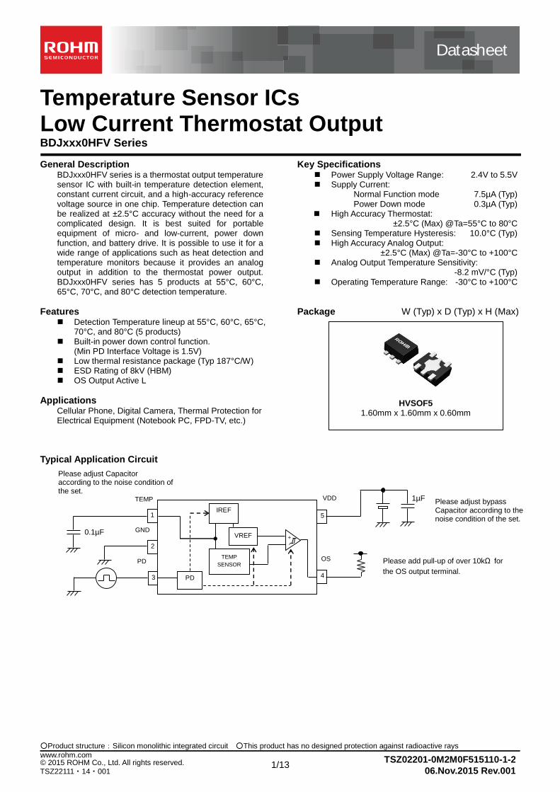
○Product structure:Silicon monolithic integrated circuit ○This product has no designed protection against radioactive rays . 1/13 TSZ02201-0M2M0F515110-1-2 © 2015 ROHM Co., Ltd. All rights reserved. 06.Nov.2015 Rev.001 TSZ22111・14・001 www.rohm.com Temperature Sensor ICs Low Current Thermostat Output BDJxxx0HFV Series General Description BDJxxx0HFV series is a thermostat output temperature sensor IC with built-in temperature detection element, constant current circuit, and a high-accuracy reference voltage source in one chip. Temperature detection can be realized at ±2.5°C accuracy without the need for a complicated design. It is best suited for portable equipment of micro- and low-current, power down function, and battery drive. It is possible to use it for a wide range of applications such as heat detection and temperature monitors because it provides an analog output in addition to the thermostat power output. BDJxxx0HFV series has 5 products at 55°C, 60°C, 65°C, 70°C, and 80°C detection temperature. Features Detection Temperature lineup at 55°C, 60°C, 65°C, 70°C, and 80°C (5 products) Built-in power down control function. (Min PD Interface Voltage is 1.5V) Low thermal resistance package (Typ 187°C/W) ESD Rating of 8kV (HBM) OS Output Active L Applications Cellular Phone, Digital Camera, Thermal Protection for Electrical Equipment (Notebook PC, FPD-TV, etc.) Key Specifications Power Supply Voltage Range: 2.4V to 5.5V Supply Current: Normal Function mode 7.5μA (Typ) Power Down mode 0.3μA (Typ) High Accuracy Thermostat: ±2.5°C (Max) @Ta=55°C to 80°C Sensing Temperature Hysteresis: 10.0°C (Typ) High Accuracy Analog Output: ±2.5°C (Max) @Ta=-30°C to +100°C Analog Output Temperature Sensitivity: -8.2 mV/°C (Typ) Operating Temperature Range: -30°C to +100°C Package W (Typ) x D (Typ) x H (Max) Typical Application Circuit HVSOF5 1.60mm x 1.60mm x 0.60mm Please adjust Capacitor according to the noise condition of the set. GND TEMP PD VREF TEMP SENSOR VDD OS IREF + - 1 2 3 5 C 4 PD 0.1μF Please adjust bypass Capacitor according to the noise condition of the set. 1μF Please add pull-up of over 10kΩ for the OS output terminal. Datasheet Datasheet
Transcript of Temperature Sensor ICs Low Current Thermostat...
○Product structure:Silicon monolithic integrated circuit ○This product has no designed protection against radioactive rays
.
1/13 TSZ02201-0M2M0F515110-1-2 © 2015 ROHM Co., Ltd. All rights reserved.
06.Nov.2015 Rev.001 TSZ22111・14・001
www.rohm.com
Temperature Sensor ICs Low Current Thermostat Output BDJxxx0HFV Series
General Description BDJxxx0HFV series is a thermostat output temperature sensor IC with built-in temperature detection element, constant current circuit, and a high-accuracy reference voltage source in one chip. Temperature detection can be realized at ±2.5°C accuracy without the need for a complicated design. It is best suited for portable equipment of micro- and low-current, power down function, and battery drive. It is possible to use it for a wide range of applications such as heat detection and temperature monitors because it provides an analog output in addition to the thermostat power output. BDJxxx0HFV series has 5 products at 55°C, 60°C, 65°C, 70°C, and 80°C detection temperature.
Features Detection Temperature lineup at 55°C, 60°C, 65°C,
70°C, and 80°C (5 products) Built-in power down control function.
(Min PD Interface Voltage is 1.5V) Low thermal resistance package (Typ 187°C/W) ESD Rating of 8kV (HBM) OS Output Active L
Applications Cellular Phone, Digital Camera, Thermal Protection for Electrical Equipment (Notebook PC, FPD-TV, etc.)
Key Specifications
Power Supply Voltage Range: 2.4V to 5.5V Supply Current:
Normal Function mode 7.5µA (Typ) Power Down mode 0.3µA (Typ)
High Accuracy Thermostat: ±2.5°C (Max) @Ta=55°C to 80°C
Sensing Temperature Hysteresis: 10.0°C (Typ) High Accuracy Analog Output:
±2.5°C (Max) @Ta=-30°C to +100°C Analog Output Temperature Sensitivity:
-8.2 mV/°C (Typ) Operating Temperature Range: -30°C to +100°C
Package W (Typ) x D (Typ) x H (Max)
Typical Application Circuit
HVSOF5 1.60mm x 1.60mm x 0.60mm
Please adjust Capacitor according to the noise condition of the set.
GND
TEMP
PD
VREF
TEMP
SENSOR
VDD
OS
IREF
+ -
1
C
2
3
5
C
4
PD
0.1µF
Please adjust bypass Capacitor according to the noise condition of the set.
1µF
Please add pull-up of over 10kΩ for
the OS output terminal.
Datasheet
Datasheet
BDJxxx0HFV Series
2/13
TSZ02201-0M2M0F515110-1-2 © 2015 ROHM Co., Ltd. All rights reserved. 06.Nov.2015 Rev.001
www.rohm.com
TSZ22111 • 15 • 001
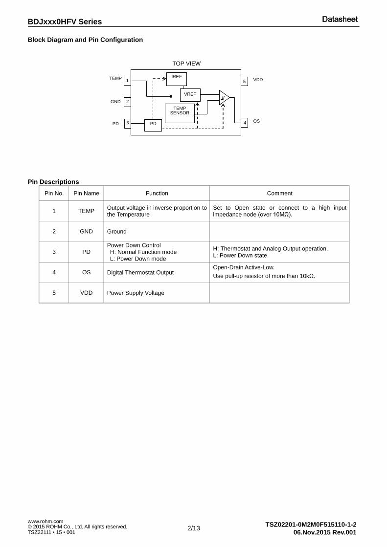
Block Diagram and Pin Configuration
Pin Descriptions
Pin No. Pin Name Function Comment
1 TEMP Output voltage in inverse proportion to the Temperature
Set to Open state or connect to a high input impedance node (over 10MΩ).
2 GND Ground
3 PD Power Down Control H: Normal Function mode L: Power Down mode
H: Thermostat and Analog Output operation. L: Power Down state.
4 OS Digital Thermostat Output Open-Drain Active-Low.
Use pull-up resistor of more than 10kΩ.
5 VDD Power Supply Voltage
TOP VIEW
GND
TEMP
PD
VREF
TEMP SENSOR
VDD
OS
IREF
1
2
3
5
4 PD
BDJxxx0HFV Series
3/13
TSZ02201-0M2M0F515110-1-2 © 2015 ROHM Co., Ltd. All rights reserved. 06.Nov.2015 Rev.001
www.rohm.com
TSZ22111 • 15 • 001
Absolute Maximum Ratings (Ta=25°C)
Parameter Symbol Rating Unit
Power Supply Voltage VDD -0.3 to +7.0 (Note 1) V
Input Voltage (PD) VIN -0.3 to +VDD+0.3 V
OS Terminal Voltage VOS -0.3 to +7.0 (Note 1) V
OS Terminal Current IOS 5.0 mA
Power Dissipation Pd 0.53 (Note 2) W
Storage Temperature Range Tstg -55 to +150 °C
(Note 1) However, not exceeding Pd. (Note 2) When mounted on ROHM standard board, derate by 5.36mW/°C for Ta higher than 25°C. Caution: Operating the IC over the absolute maximum ratings may damage the IC. The damage can either be a short circuit between pins or an open circuit
between pins and the internal circuitry. Therefore, it is important to consider circuit protection measures, such as adding a fuse, in case the IC is operated over the absolute maximum ratings.
Recommended Operating Conditions
Parameter Symbol Rating
Unit Min Typ Max
Power Supply Voltage VDD 2.4 2.8 5.5 V
Operating Temperature Range Topr -30 - +100 °C
Electrical Characteristics (Unless otherwise specified, VDD = 2.8V, Ta = 25°C)
Parameter Symbol Limit
Unit Conditions Min Typ Max
Supply Current
Normal Function Mode IDD - 7.5 12.0 µA PD=“H”
Power Down Mode IDDPD - 0.3 1.0 µA PD=“L”
PD
Input L Voltage VIL GND - 0.2 V
Input H Voltage VIH 1.5 - VDD V
PD Leakage Current ILPD - - 1.0 µA PD=2.8V
Analog Output
TEMP Output Voltage VTEMP 1.279 1.300 1.321 V Ta = 30°C
TEMP Temperature Sensitivity VSE -8.00 -8.20 -8.40 mV/°C Ta = -30°C to +100°C
TEMP Load Regulation ΔVTEMPRL - - 1.0 mV Difference Of IOUT : 0µA / 2µA
TEMP VDD Regulation ΔVTEMPVDD - - 4.0 mV VDD=2.4V to 5.5V
OS Output Open Drain
OS Leakage Current IL - - 1.0 µA VOS =5.0V
OS Output Voltage VOL - - 0.4 V IOS = 1.0mA
Temperature Accuracy (Unless otherwise specified, VDD = 2.8V)
Parameter Symbol Limit
Unit Conditions Min Typ Max
Thermostat
Sensing Temperature Accuracy Tacc - - ±2.5 °C
Sensing Temperature Hysteresis Thys 7.5 10.0 12.5 °C
Analog Output
TEMP Temperature Accuracy TTEMP - - ±2.5 °C VDD = 2.8V Ta = -30°C to +100°C
BDJxxx0HFV Series
4/13
TSZ02201-0M2M0F515110-1-2 © 2015 ROHM Co., Ltd. All rights reserved. 06.Nov.2015 Rev.001
www.rohm.com
TSZ22111 • 15 • 001
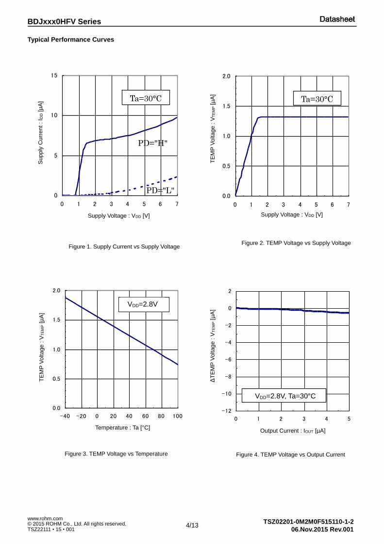
Typical Performance Curves
0.0
0.5
1.0
1.5
2.0
-40 -20 0 20 40 60 80 100
Temp[℃]
Vte
mp[
V]
VDD=2.8
V
VDD=2.8V
Figure 1. Supply Current vs Supply Voltage
0
5
10
15
0 1 2 3 4 5 6 7
VDD [V]
IDD
[μ
A]
Ta=30°C
PD="H"
PD="L"
Supply Voltage : VDD [V]
Su
pp
ly C
urr
en
t :
I DD [
µA
]
Figure 4. TEMP Voltage vs Output Current
-12
-10
-8
-6
-4
-2
0
2
0 1 2 3 4 5
Iout [uA]
⊿V
tem
p [m
V]
VDD=2.8V, Ta=30°C
Output Current : IOUT [µA]
ΔT
EM
P V
oltag
e :
VT
EM
P [
µA
]
VDD=2.8V, Ta=30°C
Figure 3. TEMP Voltage vs Temperature
Temperature : Ta [°C]
TE
MP
Vo
ltag
e :
VT
EM
P [
µA
]
VDD=2.8V
Figure 2. TEMP Voltage vs Supply Voltage
0.0
0.5
1.0
1.5
2.0
0 1 2 3 4 5 6 7
VDD [V]V
tem
p [V
]
Ta=30°C
Supply Voltage : VDD [V] T
EM
P V
oltag
e :
VT
EM
P [
µA
]
BDJxxx0HFV Series
5/13
TSZ02201-0M2M0F515110-1-2 © 2015 ROHM Co., Ltd. All rights reserved. 06.Nov.2015 Rev.001
www.rohm.com
TSZ22111 • 15 • 001
Typical Performance Curves – continued
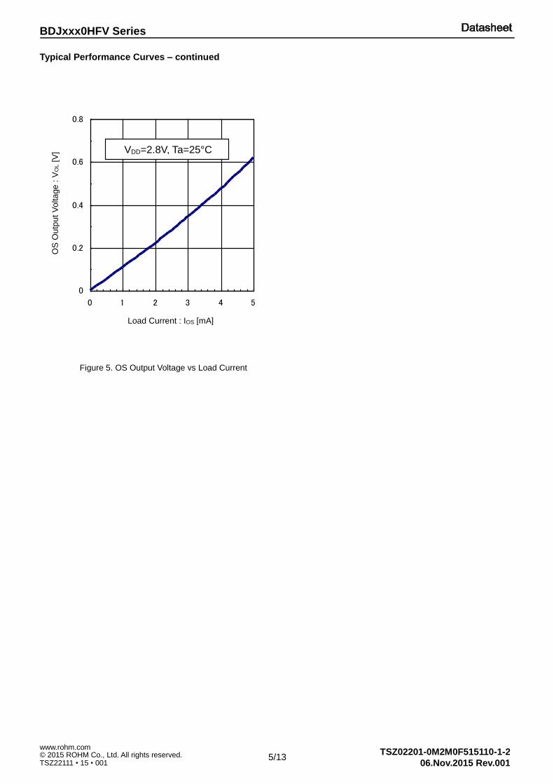
Figure 5. OS Output Voltage vs Load Current
0
0.2
0.4
0.6
0.8
0 1 2 3 4 5
IOS [mA]
V O
L[V
]
VDD=2.8V, Ta=25°C
Load Current : IOS [mA]
OS
Ou
tpu
t V
olta
ge
: V
OL [V
] VDD=2.8V, Ta=25°C
BDJxxx0HFV Series
6/13
TSZ02201-0M2M0F515110-1-2 © 2015 ROHM Co., Ltd. All rights reserved. 06.Nov.2015 Rev.001
www.rohm.com
TSZ22111 • 15 • 001
Application Information
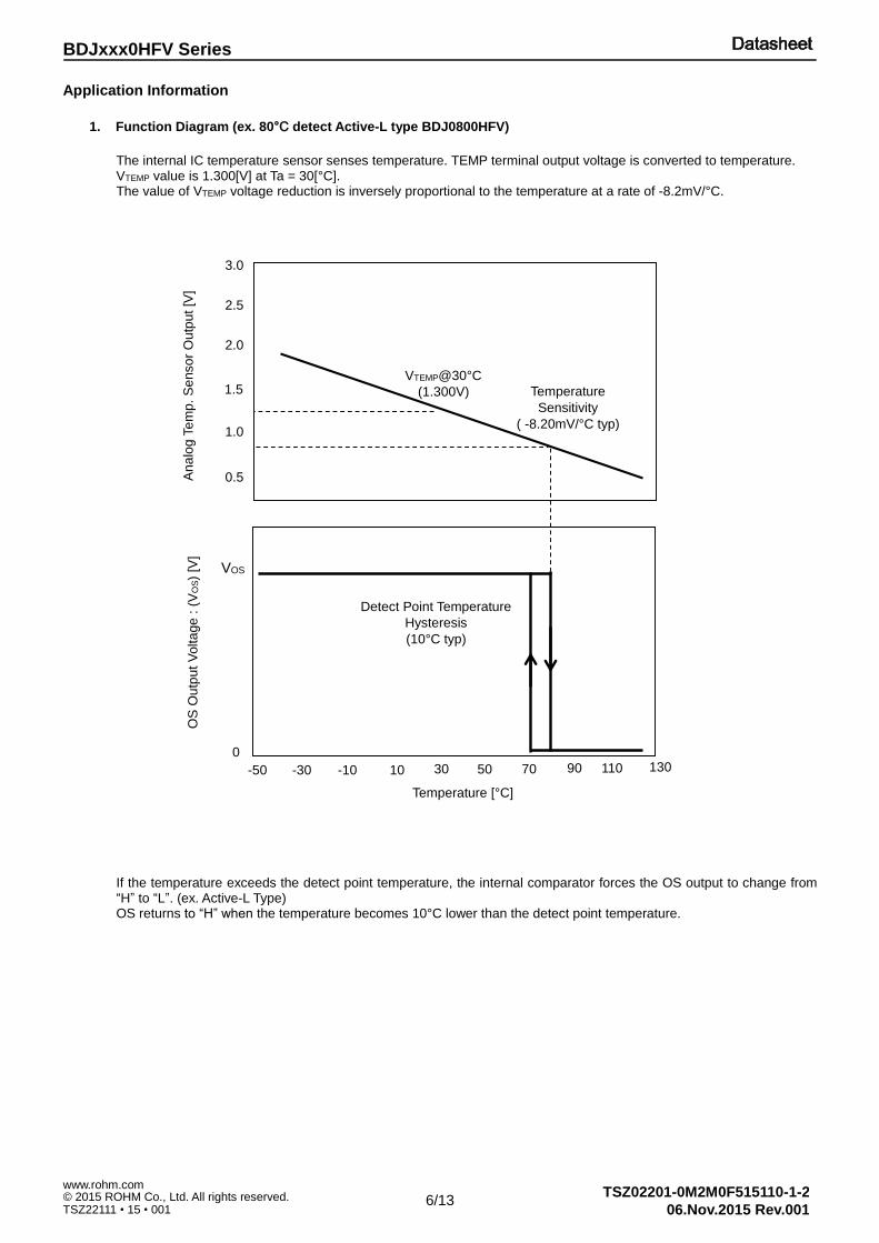
1. Function Diagram (ex. 80°C detect Active-L type BDJ0800HFV)
The internal IC temperature sensor senses temperature. TEMP terminal output voltage is converted to temperature. VTEMP value is 1.300[V] at Ta = 30[°C]. The value of VTEMP voltage reduction is inversely proportional to the temperature at a rate of -8.2mV/°C.
If the temperature exceeds the detect point temperature, the internal comparator forces the OS output to change from “H” to “L”. (ex. Active-L Type) OS returns to “H” when the temperature becomes 10°C lower than the detect point temperature.
2.0
An
alo
g T
em
p.
Se
nso
r O
utp
ut [V
] O
S O
utp
ut
Volta
ge
: (
VO
S)
[V]
0
1.0
VOS
VTEMP@30°C
(1.300V) Temperature
Sensitivity
( -8.20mV/°C typ)
Detect Point Temperature
Hysteresis
(10°C typ)
110 90 70 50 10 130 -30 30 -10 -50
Temperature [°C]
1.5
2.5
3.0
0.5
BDJxxx0HFV Series
7/13
TSZ02201-0M2M0F515110-1-2 © 2015 ROHM Co., Ltd. All rights reserved. 06.Nov.2015 Rev.001
www.rohm.com
TSZ22111 • 15 • 001
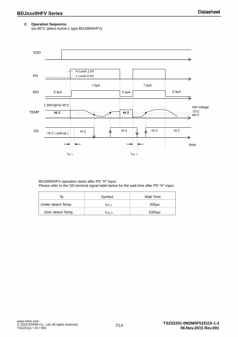
2. Operation Sequence
(ex.80°C detect Active-L type BDJ0800HFV)
BDJ0800HFV operation starts after PD “H” Input. Please refer to the OS terminal signal table below for the wait time after PD “H” Input.
Ta Symbol Wait Time
Under detect Temp. tOS_L 200µs
Over detect Temp. tOS_H 1000µs
Ref Voltage
VDD
Hi Z(pull-up) Hi Z Hi Z
1.300V@Ta=30°C
0.3µA 0.3µA
7.5µA
L Level 0.2V PD
IDD
TEMP
OS
time
70°C 80°C
H Level 1.5V
Hi Z Hi Z
7.5µA
0.3µA
Hi Z
tOS_L
tOS_H
Hi Z
BDJxxx0HFV Series
8/13
TSZ02201-0M2M0F515110-1-2 © 2015 ROHM Co., Ltd. All rights reserved. 06.Nov.2015 Rev.001
www.rohm.com
TSZ22111 • 15 • 001
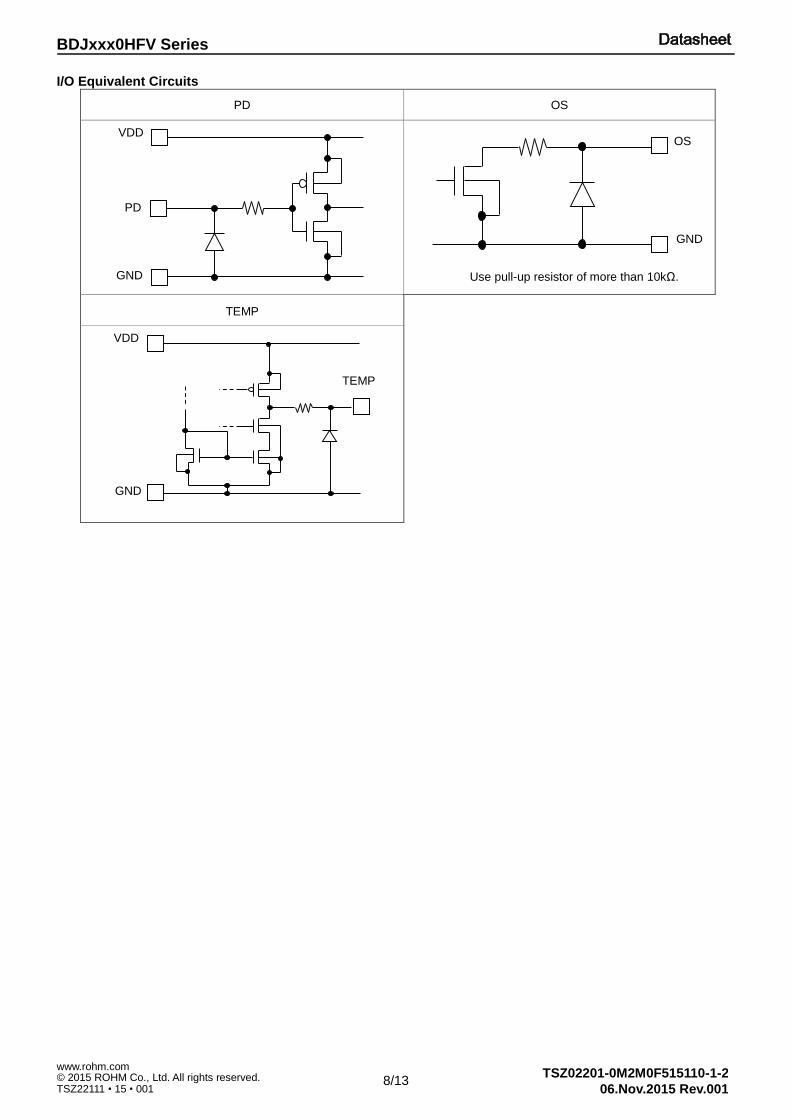
I/O Equivalent Circuits
PD OS
TEMP
VDD
GND Use pull-up resistor of more than 10kΩ.
GND
OS
PD
GND
VDD
TEMP
BDJxxx0HFV Series
9/13
TSZ02201-0M2M0F515110-1-2 © 2015 ROHM Co., Ltd. All rights reserved. 06.Nov.2015 Rev.001
www.rohm.com
TSZ22111 • 15 • 001
Operational Notes
1. Reverse Connection of Power Supply
Connecting the power supply in reverse polarity can damage the IC. Take precautions against reverse polarity when connecting the power supply, such as mounting an external diode between the power supply and the IC’s power supply pins.
2. Power Supply Lines
Design the PCB layout pattern to provide low impedance supply lines. Separate the ground and supply lines of the digital and analog blocks to prevent noise in the ground and supply lines of the digital block from affecting the analog block. Furthermore, connect a capacitor to ground at all power supply pins. Consider the effect of temperature and aging on the capacitance value when using electrolytic capacitors.
3. Ground Voltage
Ensure that no pins are at a voltage below that of the ground pin at any time, even during transient condition.
4. Ground Wiring Pattern
When using both small-signal and large-current ground traces, the two ground traces should be routed separately but connected to a single ground at the reference point of the application board to avoid fluctuations in the small-signal ground caused by large currents. Also ensure that the ground traces of external components do not cause variations on the ground voltage. The ground lines must be as short and thick as possible to reduce line impedance.
5. Thermal Consideration
Should by any chance the power dissipation rating be exceeded the rise in temperature of the chip may result in deterioration of the properties of the chip. In case of exceeding this absolute maximum rating, increase the board size and copper area to prevent exceeding the Pd rating.
6. Recommended Operating Conditions
These conditions represent a range within which the expected characteristics of the IC can be approximately obtained. The electrical characteristics are guaranteed under the conditions of each parameter.
7. Inrush Current
When power is first supplied to the IC, it is possible that the internal logic may be unstable and inrush current may flow instantaneously due to the internal powering sequence and delays, especially if the IC has more than one power supply. Therefore, give special consideration to power coupling capacitance, power wiring, width of ground wiring, and routing of connections.
8. Operation Under Strong Electromagnetic Field
Operating the IC in the presence of a strong electromagnetic field may cause the IC to malfunction.
9. Testing on Application Boards
When testing the IC on an application board, connecting a capacitor directly to a low-impedance output pin may subject the IC to stress. Always discharge capacitors completely after each process or step. The IC’s power supply should always be turned off completely before connecting or removing it from the test setup during the inspection process. To prevent damage from static discharge, ground the IC during assembly and use similar precautions during transport and storage.
10. Inter-pin Short and Mounting Errors
Ensure that the direction and position are correct when mounting the IC on the PCB. Incorrect mounting may result in damaging the IC. Avoid nearby pins being shorted to each other especially to ground, power supply and output pin. Inter-pin shorts could be due to many reasons such as metal particles, water droplets (in very humid environment) and unintentional solder bridge deposited in between pins during assembly to name a few.

BDJxxx0HFV Series
10/13
TSZ02201-0M2M0F515110-1-2 © 2015 ROHM Co., Ltd. All rights reserved. 06.Nov.2015 Rev.001
www.rohm.com
TSZ22111 • 15 • 001
Operational Notes – continued
11. Unused Input Pins
Input pins of an IC are often connected to the gate of a MOS transistor. The gate has extremely high impedance and extremely low capacitance. If left unconnected, the electric field from the outside can easily charge it. The small charge acquired in this way is enough to produce a significant effect on the conduction through the transistor and cause unexpected operation of the IC. So unless otherwise specified, unused input pins should be connected to the power supply or ground line.
12. Regarding the Input Pin of the IC
This monolithic IC contains P+ isolation and P substrate layers between adjacent elements in order to keep them isolated. P-N junctions are formed at the intersection of the P layers with the N layers of other elements, creating a parasitic diode or transistor. For example (refer to figure below):
When GND > Pin A and GND > Pin B, the P-N junction operates as a parasitic diode. When GND > Pin B, the P-N junction operates as a parasitic transistor.
Parasitic diodes inevitably occur in the structure of the IC. The operation of parasitic diodes can result in mutual interference among circuits, operational faults, or physical damage. Therefore, conditions that cause these diodes to operate, such as applying a voltage lower than the GND voltage to an input pin (and thus to the P substrate) should be avoided.
Figure 6. Example of monolithic IC structure
N NP
+ P
N NP
+
P Substrate
GND
NP
+
N NP
+N P
P Substrate
GND GND
Parasitic
Elements
Pin A
Pin A
Pin B Pin B
B C
E
Parasitic
Elements
GNDParasitic
Elements
CB
E
Transistor (NPN)Resistor
N Region
close-by
Parasitic
Elements
BDJxxx0HFV Series
11/13
TSZ02201-0M2M0F515110-1-2 © 2015 ROHM Co., Ltd. All rights reserved. 06.Nov.2015 Rev.001
www.rohm.com
TSZ22111 • 15 • 001
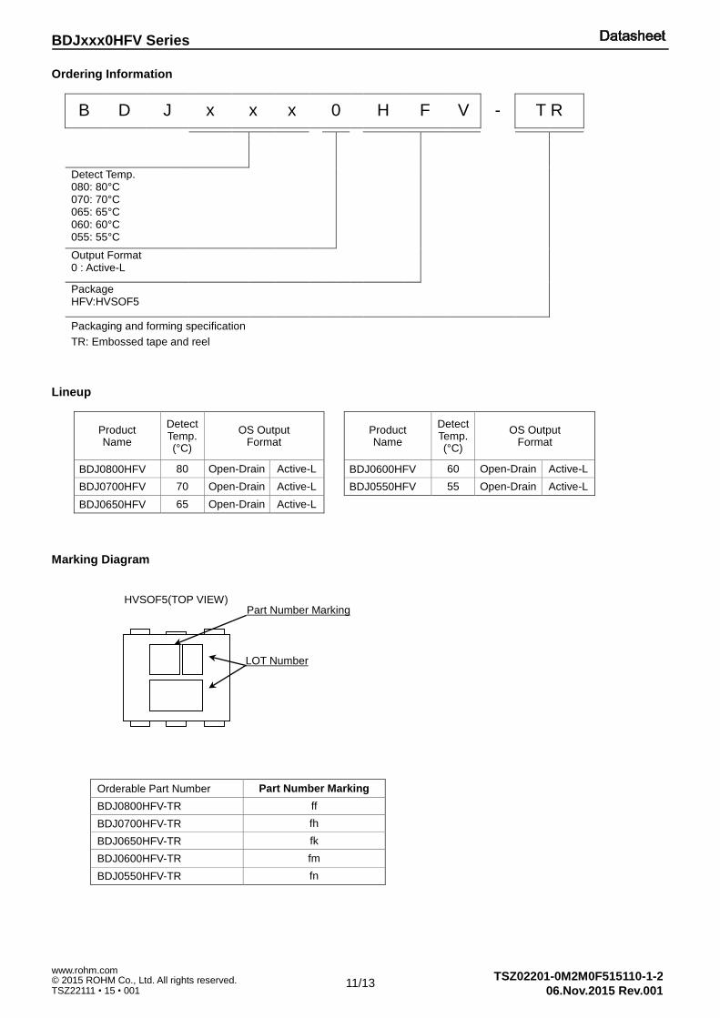
Ordering Information
B D J x x x
0
H F V - T R
Detect Temp. 080: 80°C 070: 70°C 065: 65°C 060: 60°C 055: 55°C
Output Format 0 : Active-L
Package HFV:HVSOF5
Packaging and forming specification
TR: Embossed tape and reel
Lineup
Product Name
Detect Temp. (°C)
OS Output Format
Product Name
Detect Temp. (°C)
OS Output Format
BDJ0800HFV 80 Open-Drain Active-L BDJ0600HFV 60 Open-Drain Active-L
BDJ0700HFV 70 Open-Drain Active-L BDJ0550HFV 55 Open-Drain Active-L
BDJ0650HFV 65 Open-Drain Active-L
Marking Diagram
Orderable Part Number Part Number Marking
BDJ0800HFV-TR ff
BDJ0700HFV-TR fh
BDJ0650HFV-TR fk
BDJ0600HFV-TR fm
BDJ0550HFV-TR fn
HVSOF5(TOP VIEW)
Part Number Marking
LOT Number
BDJxxx0HFV Series
12/13
TSZ02201-0M2M0F515110-1-2 © 2015 ROHM Co., Ltd. All rights reserved. 06.Nov.2015 Rev.001
www.rohm.com
TSZ22111 • 15 • 001
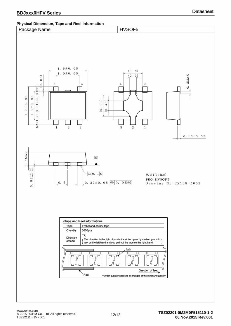
Physical Dimension, Tape and Reel Information
Package Name HVSOF5
BDJxxx0HFV Series
13/13
TSZ02201-0M2M0F515110-1-2 © 2015 ROHM Co., Ltd. All rights reserved. 06.Nov.2015 Rev.001
www.rohm.com
TSZ22111 • 15 • 001
Revision History
Date Revision Changes
06.Nov.2015 001 New Release
DatasheetDatasheet
Notice-PGA-E Rev.002© 2015 ROHM Co., Ltd. All rights reserved.
Notice Precaution on using ROHM Products
1. Our Products are designed and manufactured for application in ordinary electronic equipments (such as AV equipment, OA equipment, telecommunication equipment, home electronic appliances, amusement equipment, etc.). If you intend to use our Products in devices requiring extremely high reliability (such as medical equipment (Note 1), transport equipment, traffic equipment, aircraft/spacecraft, nuclear power controllers, fuel controllers, car equipment including car accessories, safety devices, etc.) and whose malfunction or failure may cause loss of human life, bodily injury or serious damage to property (“Specific Applications”), please consult with the ROHM sales representative in advance. Unless otherwise agreed in writing by ROHM in advance, ROHM shall not be in any way responsible or liable for any damages, expenses or losses incurred by you or third parties arising from the use of any ROHM’s Products for Specific Applications.
(Note1) Medical Equipment Classification of the Specific Applications JAPAN USA EU CHINA
CLASSⅢ CLASSⅢ
CLASSⅡb CLASSⅢ
CLASSⅣ CLASSⅢ
2. ROHM designs and manufactures its Products subject to strict quality control system. However, semiconductor
products can fail or malfunction at a certain rate. Please be sure to implement, at your own responsibilities, adequate safety measures including but not limited to fail-safe design against the physical injury, damage to any property, which a failure or malfunction of our Products may cause. The following are examples of safety measures:
[a] Installation of protection circuits or other protective devices to improve system safety [b] Installation of redundant circuits to reduce the impact of single or multiple circuit failure
3. Our Products are designed and manufactured for use under standard conditions and not under any special or extraordinary environments or conditions, as exemplified below. Accordingly, ROHM shall not be in any way responsible or liable for any damages, expenses or losses arising from the use of any ROHM’s Products under any special or extraordinary environments or conditions. If you intend to use our Products under any special or extraordinary environments or conditions (as exemplified below), your independent verification and confirmation of product performance, reliability, etc, prior to use, must be necessary:
[a] Use of our Products in any types of liquid, including water, oils, chemicals, and organic solvents [b] Use of our Products outdoors or in places where the Products are exposed to direct sunlight or dust [c] Use of our Products in places where the Products are exposed to sea wind or corrosive gases, including Cl2,
H2S, NH3, SO2, and NO2
[d] Use of our Products in places where the Products are exposed to static electricity or electromagnetic waves [e] Use of our Products in proximity to heat-producing components, plastic cords, or other flammable items [f] Sealing or coating our Products with resin or other coating materials [g] Use of our Products without cleaning residue of flux (even if you use no-clean type fluxes, cleaning residue of
flux is recommended); or Washing our Products by using water or water-soluble cleaning agents for cleaning residue after soldering
[h] Use of the Products in places subject to dew condensation
4. The Products are not subject to radiation-proof design. 5. Please verify and confirm characteristics of the final or mounted products in using the Products. 6. In particular, if a transient load (a large amount of load applied in a short period of time, such as pulse. is applied,
confirmation of performance characteristics after on-board mounting is strongly recommended. Avoid applying power exceeding normal rated power; exceeding the power rating under steady-state loading condition may negatively affect product performance and reliability.
7. De-rate Power Dissipation depending on ambient temperature. When used in sealed area, confirm that it is the use in
the range that does not exceed the maximum junction temperature. 8. Confirm that operation temperature is within the specified range described in the product specification. 9. ROHM shall not be in any way responsible or liable for failure induced under deviant condition from what is defined in
this document.
Precaution for Mounting / Circuit board design 1. When a highly active halogenous (chlorine, bromine, etc.) flux is used, the residue of flux may negatively affect product
performance and reliability.
2. In principle, the reflow soldering method must be used on a surface-mount products, the flow soldering method must be used on a through hole mount products. If the flow soldering method is preferred on a surface-mount products, please consult with the ROHM representative in advance.
For details, please refer to ROHM Mounting specification

DatasheetDatasheet
Notice-PGA-E Rev.002© 2015 ROHM Co., Ltd. All rights reserved.
Precautions Regarding Application Examples and External Circuits 1. If change is made to the constant of an external circuit, please allow a sufficient margin considering variations of the
characteristics of the Products and external components, including transient characteristics, as well as static characteristics.
2. You agree that application notes, reference designs, and associated data and information contained in this document
are presented only as guidance for Products use. Therefore, in case you use such information, you are solely responsible for it and you must exercise your own independent verification and judgment in the use of such information contained in this document. ROHM shall not be in any way responsible or liable for any damages, expenses or losses incurred by you or third parties arising from the use of such information.
Precaution for Electrostatic
This Product is electrostatic sensitive product, which may be damaged due to electrostatic discharge. Please take proper caution in your manufacturing process and storage so that voltage exceeding the Products maximum rating will not be applied to Products. Please take special care under dry condition (e.g. Grounding of human body / equipment / solder iron, isolation from charged objects, setting of Ionizer, friction prevention and temperature / humidity control).
Precaution for Storage / Transportation 1. Product performance and soldered connections may deteriorate if the Products are stored in the places where:
[a] the Products are exposed to sea winds or corrosive gases, including Cl2, H2S, NH3, SO2, and NO2 [b] the temperature or humidity exceeds those recommended by ROHM [c] the Products are exposed to direct sunshine or condensation [d] the Products are exposed to high Electrostatic
2. Even under ROHM recommended storage condition, solderability of products out of recommended storage time period may be degraded. It is strongly recommended to confirm solderability before using Products of which storage time is exceeding the recommended storage time period.
3. Store / transport cartons in the correct direction, which is indicated on a carton with a symbol. Otherwise bent leads
may occur due to excessive stress applied when dropping of a carton. 4. Use Products within the specified time after opening a humidity barrier bag. Baking is required before using Products of
which storage time is exceeding the recommended storage time period.
Precaution for Product Label QR code printed on ROHM Products label is for ROHM’s internal use only.
Precaution for Disposition When disposing Products please dispose them properly using an authorized industry waste company.
Precaution for Foreign Exchange and Foreign Trade act Since concerned goods might be fallen under listed items of export control prescribed by Foreign exchange and Foreign trade act, please consult with ROHM in case of export.
Precaution Regarding Intellectual Property Rights 1. All information and data including but not limited to application example contained in this document is for reference
only. ROHM does not warrant that foregoing information or data will not infringe any intellectual property rights or any other rights of any third party regarding such information or data.
2. ROHM shall not have any obligations where the claims, actions or demands arising from the combination of the Products with other articles such as components, circuits, systems or external equipment (including software).
3. No license, expressly or implied, is granted hereby under any intellectual property rights or other rights of ROHM or any third parties with respect to the Products or the information contained in this document. Provided, however, that ROHM will not assert its intellectual property rights or other rights against you or your customers to the extent necessary to manufacture or sell products containing the Products, subject to the terms and conditions herein.
Other Precaution 1. This document may not be reprinted or reproduced, in whole or in part, without prior written consent of ROHM.
2. The Products may not be disassembled, converted, modified, reproduced or otherwise changed without prior written consent of ROHM.
3. In no event shall you use in any way whatsoever the Products and the related technical information contained in the Products or this document for any military purposes, including but not limited to, the development of mass-destruction weapons.
4. The proper names of companies or products described in this document are trademarks or registered trademarks of ROHM, its affiliated companies or third parties.
DatasheetDatasheet
Notice – WE Rev.001© 2015 ROHM Co., Ltd. All rights reserved.
General Precaution 1. Before you use our Pro ducts, you are requested to care fully read this document and fully understand its contents.
ROHM shall n ot be in an y way responsible or liabl e for fa ilure, malfunction or acci dent arising from the use of a ny ROHM’s Products against warning, caution or note contained in this document.
2. All information contained in this docume nt is current as of the issuing date and subj ect to change without any prior
notice. Before purchasing or using ROHM’s Products, please confirm the la test information with a ROHM sale s representative.
3. The information contained in this doc ument is provi ded on an “as is” basis and ROHM does not warrant that all
information contained in this document is accurate an d/or error-free. ROHM shall not be in an y way responsible or liable for any damages, expenses or losses incurred by you or third parties resulting from inaccuracy or errors of or concerning such information.