Temperature Gradient Alleviating Method for Arithmetic … · temperature gradient alleviating...
7
HAL Id: hal-00189468 https://hal.archives-ouvertes.fr/hal-00189468 Submitted on 21 Nov 2007 HAL is a multi-disciplinary open access archive for the deposit and dissemination of sci- entific research documents, whether they are pub- lished or not. The documents may come from teaching and research institutions in France or abroad, or from public or private research centers. L’archive ouverte pluridisciplinaire HAL, est destinée au dépôt et à la diffusion de documents scientifiques de niveau recherche, publiés ou non, émanant des établissements d’enseignement et de recherche français ou étrangers, des laboratoires publics ou privés. Temperature Gradient Alleviating Method for Arithmetic Units R. Egawa, M. Ito, N. Hasegawa, T. Nakamura To cite this version: R. Egawa, M. Ito, N. Hasegawa, T. Nakamura. Temperature Gradient Alleviating Method for Arith- metic Units. THERMINIC 2005, Sep 2005, Belgirate, Lago Maggiore, Italy. TIMA Editions, pp.151- 156, 2005. <hal-00189468>
Transcript of Temperature Gradient Alleviating Method for Arithmetic … · temperature gradient alleviating...
HAL Id: hal-00189468https://hal.archives-ouvertes.fr/hal-00189468
Submitted on 21 Nov 2007
HAL is a multi-disciplinary open accessarchive for the deposit and dissemination of sci-entific research documents, whether they are pub-lished or not. The documents may come fromteaching and research institutions in France orabroad, or from public or private research centers.
L’archive ouverte pluridisciplinaire HAL, estdestinée au dépôt et à la diffusion de documentsscientifiques de niveau recherche, publiés ou non,émanant des établissements d’enseignement et derecherche français ou étrangers, des laboratoirespublics ou privés.
Temperature Gradient Alleviating Method forArithmetic Units
R. Egawa, M. Ito, N. Hasegawa, T. Nakamura
To cite this version:R. Egawa, M. Ito, N. Hasegawa, T. Nakamura. Temperature Gradient Alleviating Method for Arith-metic Units. THERMINIC 2005, Sep 2005, Belgirate, Lago Maggiore, Italy. TIMA Editions, pp.151-156, 2005. <hal-00189468>

Belgirate, Italy, 28-30 September 2005
TEMPERATURE GRADIENT ALLEVIATING METHODS FOR ARITHMETIC UNITS
Ryusuke EGAWA, Mutsuo ITO, Naoyuki HASEGAWA, Ken-ichi SUZUKI, and Tadao NAKAMURA
Graduate School of Information Sciences, Tohoku University, Sendai 980-9570, Japan
E-mail: {egawa, mutsu, nhsos, suzuki, [email protected]}
ABSTRACT
Recently, thermal-aware digital circuit design in advanced
technologies is great challenges to realize high-speed and
robust microprocessors. In this paper, we explore
temperature gradient alleviating method for arithmetic
units. Aiming at alleviating temperature gradients at
logical circuit design level, we try to flatten out a power
density by applying delay-balancing technique for equal-
delay circuits. Our proposal is evaluated in fine grain
thermal simulation. Simulation results show the strong
dependency between placement and temperature gradients
on arithmetic units.
.
1. INTRODUCTION
Computer architects and circuit designers are
continually pushing the envelope in the race to design
faster, powerful microprocessors. Technology scaling to
advanced technologies brings higher performance and
higher levels of on-chip functional integration. However,
this scaling has brought with it a variety of exacerbated
issues, such as higher current and power densities,
increased leakage current, low-k dielectrics with poorer
heat conductivity, and package and heat sink design
challenges. In other words, the rapid increase in speed
and complexity of recent microprocessors is outstripping
the benefit of feature size scaling and supply voltage
reduction. Furthermore the power density has doubled
every three years in recent microprocessors. As a result,
the temperature of the microprocessor increases rapidly,
and high temperature causes speed degradation of
transistors and increase in cooling cost. Consequently,
thermal aware design will play the key role in future
VLSI design as well as power conscious design [1]. The
“hot spot”, the area where a temperature is locally high,
generates a large temperature gradient as for not only
microprocessors but also functional blocks, and
deteriorates the robustness or reliability of the
microprocessors in DSM (Deep Sub-Micron era) [2]. [4] reported that there is about nine degree temperature difference even in a 10-bit negative adder. Based on the
above facts, in advanced CMOS technologies, an early
accurate design estimation including deep submicron
effects is strongly required.
Aiming to clarify the thermal behavior on VLSI, and
to design thermal robust microprocessors in DSM, many
researchers have studied thermal simulation methods by
various approaches. The simulator proposed in [2],
“hotspot”, is based on instruction level and functional unit
analysis. On the other hand, simulators, “ILLIADS-T” [4]
and “THERMAN” [10], proposed finer grain thermal
simulations based on the switching of transistors and
logic gates. However, they employ steady-state
temperature analysis in temporal granularity for the
reason that the time required for the on chip temperature
to reach its steady-state is several order of magnitude
longer the clock signal period in digital circuits. These
approaches are fine enough for evaluating rough thermal
behavior of large-scale integrated circuits. But, to
examine temperature behavior in a functional unit, more
detailed or fine temporal granularity is needed. [5]
proposed finer grain thermal simulation to evaluate
detailed inside thermal behavior of functional units. it use
a logic cell as a heat source, and evaluate the temperature
at every clock cycle level.
As mentioned above, thermal simulation methods are
studied well in late years. However, thermal aware
digital circuit design methodologies have not been so
studied well compared with thermal simulation
methodologies. Recently the temperature-aware design
flow has been proposed [3]. It insists on the ability of
estimating temperature at different granularities and at
different design stages, especially early in the design flow.
The estimated temperature at each granularity and each stage can help to design high speed and thermal robust circuit. All the decisions should use temperature as a guideline and the design should be intrinsically thermally optimized and free from thermal limitations. They have a high potential to contribute to shorten the turn-around time of circuit design in deep submicron technologies.
Based on the fact, we study a technique to make a
temperature gradient smaller in high-speed arithmetic
units for the purpose of designing thermal robust high
speed circuits. As mentioned above, a thermal gradient
TIMA EDITIONS / THERMINIC 2005 ISBN 2-916187-01-4 151

Ryusuke EGAWA, Mutsuo ITO, Naoyuki HASEGAWA, Ken-ichi SUZUKI, and Tadao NAKAMURA
TEMPERATURE GRADIENT ALLEVIATING METHODS FOR ARITHMETIC UNITS
deteriorates reliability of arithmetic units. We
concentrate to alleviate temperature gradients inside of an
arithmetic unit, because a local temperature gradient
influences the performance of an arithmetic unit rather
than global high temperature due to the improvement of
recent cooling techniques [1][4]. Thus, we focus on the
adverse effect of temperature gradient in a functional
block, and try to flatten out it to realize thermally robust
and reliable arithmetic units in DSM.
The rest of the paper is organized as follows. In section
2, we show our basic strategies of alleviating temperature
gradient method. Section 3 describes the details of our
proposal method, especially we logic depth alleviating
technique and logical effort theory. In section , we show
some experimental results and discussion of the
possibility of temperature-aware design at logical circuit
design level. Finally, Section 5 concludes this paper.
2. BASIC STRATEGIES
Thermal behavior (or profile) strongly depends on the
power density profiles. Correspondingly, power density
correlates closely with switching activity and the total
number of switchings in a whole circuit. Thus, a simple
way to alleviate the temperature gradient in a circuit is
alleviating the power density. Also, alleviating the power
density can be achieved by flattening out switching
activities or the number of switchings [12][14]. Our
approach is basically based on this way. However,
controlling switching activities for alleviating temperature
gradient are difficult due to its strong dependency on
Figure1. Number of switching on paths.
applications, or sequences of input vectors. Therefore, it
is difficult to design a logic circuit with alleviating the
temperature gradient and power density with universal
status. And also, usually arithmetic unit design for
microprocessors does not carry on with in the light of its
applications.
Under these situations, to achieve temperature
gradients alleviating at logic circuit design level, we focus
on the number of switchings on a path. Upper portion of
Figure1 shows number of switchings on all paths in a
combinational logic circuit. In this figure, vertical axis
indicates the number of switchings on a path, and
horizontal axis indicates the paths. In this case, we
assume the combinational logic circuits have n paths. As
like this figure, respective paths have diverse number of
switchings and this can be a trigger of generating thermal
gradient in a combinational logic circuit. Thus, as the first
step of our strategy, we try to alleviate the number of
switchings of all paths of arithmetic units.
To alleviate the number of switchings we employ
delay-balancing technique. Delay-balancing techniques
are popular techniques to design equal delay circuits for
wave pipeline, asynchronous circuit and data-flow
architecture [7], [8], [9]. As implied by the name, the
delay from all inputs to all outputs of a combinational
logic circuit are designed nearly the same [6]. In addition,
though it depends on input datum, the paths of an equal
delay circuit designed by delay element insertion (which
is a kind of delay balancing technique) have almost same
numbers of switchings, because the all signals go through
almost the same number of logic gates.
Figure 2. Power density profiles:
(a) original circuit, (b) delay balanced circuit.
TIMA EDITIONS / THERMINIC 2005 ISBN 2-916187-01-4 152
Ryusuke EGAWA, Mutsuo ITO, Naoyuki HASEGAWA, Ken-ichi SUZUKI, and Tadao NAKAMURA
TEMPERATURE GRADIENT ALLEVIATING METHODS FOR ARITHMETIC UNITS
Accordingly, the number of switchings on each path for
any input pattern can be made smooth by designing equal
delay circuit. Lower portion of Figure1 shows numbers
of switching on paths after delay balancing. Shaded
cuboids denote the number of switching by inserted delay
element.
As a result of delay balancing by delay elements
insertion, we assume the power density profile will be
improved as Figure 2 This figure shows basic concepts of
our strategy. Figure 2 shows power density aspects of an
arithmetic unit designed by cell-based design. In this
figure, Figure 2 (a) shows power density of the original
circuit and Figure 2 (b) shows power density of the delay
balanced circuit. White cuboids denote the number of
switchings of original cells (given circuit), and shaded
cuboids denote the number of switchings of inserted delay
elements. Actually, the circuit size or the number of cells
is increased by delay element insertion in Figure 2 (b).
Though, we can look delay elements with high numbers
of switching in Figure 2 (b) and they contribute to
alleviate power density of the circuit. Thus, from the
viewpoint of power density and temperature gradients,
equal delay circuits are very effective in and suitable for
temperature-aware circuit design.
It is well known that the placement of the cells has a
strong influence on the thermal profile. [11] has clarified
the strong relationship between thermal profile and cell
placement and proposed thermal aware cell placement to
minimize the temperature. However, we are aiming at
finding chances of temperature aware design at logic
circuit design phase, not in physical design phase (cell
placement). Thus, we just concentrate in logical circuit
design level.
Also, increasing cells causes an increase of the total
power consumption of circuit. However, we just pay
attention most in the high-speed microprocessors design
that uses CMOS technology in the near future is in a local
temperature gradient in a minute area. The detail of these
topics is discussed in section 4 with experimental results.
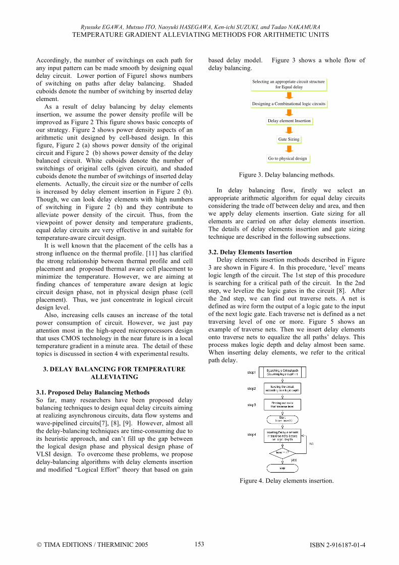
3. DELAY BALANCING FOR TEMPERATURE
ALLEVIATING
3.1. Proposed Delay Balancing Methods
So far, many researchers have been proposed delay
balancing techniques to design equal delay circuits aiming
at realizing asynchronous circuits, data flow systems and
wave-pipelined circuits[7], [8], [9]. However, almost all
the delay-balancing techniques are time-consuming due to
its heuristic approach, and can’t fill up the gap between
the logical design phase and physical design phase of
VLSI design. To overcome these problems, we propose
delay-balancing algorithms with delay elements insertion
and modified “Logical Effort” theory that based on gain
based delay model. Figure 3 shows a whole flow of
delay balancing.
Figure 3. Delay balancing methods.
In delay balancing flow, firstly we select an
appropriate arithmetic algorithm for equal delay circuits
considering the trade off between delay and area, and then
we apply delay elements insertion. Gate sizing for all
elements are carried on after delay elements insertion.
The details of delay elements insertion and gate sizing
technique are described in the following subsections.
3.2. Delay Elements Insertion
Delay elements insertion methods described in Figure
3 are shown in Figure 4. In this procedure, ‘level’ means
logic length of the circuit. The 1st step of this procedure
is searching for a critical path of the circuit. In the 2nd
step, we levelize the logic gates in the circuit [8]. After
the 2nd step, we can find out traverse nets. A net is
defined as wire form the output of a logic gate to the input
of the next logic gate. Each traverse net is defined as a net
traversing level of one or more. Figure 5 shows an
example of traverse nets. Then we insert delay elements
onto traverse nets to equalize the all paths’ delays. This
process makes logic depth and delay almost been same.
When inserting delay elements, we refer to the critical
path delay.
Figure 4. Delay elements insertion.
Selecting an appropriate circuit structure for Equal delay
Selecting an appropriate circuit structure for Equal delay
Designing a Combinational logic circuitsDesigning a Combinational logic circuits
Delay element InsertionDelay element Insertion
Gate SizingGate Sizing
Go to physical design Go to physical design
TIMA EDITIONS / THERMINIC 2005 ISBN 2-916187-01-4 153

Ryusuke EGAWA, Mutsuo ITO, Naoyuki HASEGAWA, Ken-ichi SUZUKI, and Tadao NAKAMURA
TEMPERATURE GRADIENT ALLEVIATING METHODS FOR ARITHMETIC UNITS
Figure 5. Traverse net.
3.3. Gate Sizing
In gate sizing procedure, we employ Logical Effort
(LE) based gain-based delay model due to its simplicity
and accurate delay estimation [15]. LE refers to the
inherent effort of computation in logic gates, and is a
characterization of the complexity of a logic gate. It
provides a method to estimate delay of a CMOS circuit,
and develops a scheme for sizing the transistors by back
of the envelope calculations. LE employs gain-based
delay model that has higher accuracy to estimate delay
time than commonly use wire load model. We will briefly
describe some of the main features of LE in this sub-
section. The detail of LE can be obtained from [6].
LE takes into account the fact that the speed of a
digital circuit block is dependent on its fan-out (Cout) and
fan-in (Cin). Further, LE introduces technology
independence by normalizing the speed by that of a
minimal size inverter:
dabs = d (1).
where dabs= absolute delay, d = unitless delay, = delay
of an inverter driving an identical inverter with no
parasitics. The delay expression of a logic block in LE is
given as:
d = f + p (2).
Where p = parasitic delay, f = effort or stage delay.
Further f = gh where g is defined as logical effort and h is
electrical effort. Electrical effort h is equal to the ratio of
input capacitance and output capacitance : h = Cin/Cout.
Thus:
d = gh + p (3).
The most important feature of LE is that it provides a way
of determining appropriate transistor sizing of the critical
path to minimize the delay. Optimizing the design of an
N-stage logic network proceeds from a very simple
principle: The path delay is least when each stage in the
path bears the same stage effort. In this case, each stage
bears equal effort given as:
ˆ f = gihi = F1
N (4).
In such a case, delay of the path will be equal to:
D = Nˆ f + P (5).
where, D = the path delay, F=the path effort, P = the path
parasitic delay. In order to obtain optimal transistor sizes
to realize minimal delay, gate sizing process should be
started from the output and calculate Cin for each stage,
which is determined by each stage effort.
Some modification of LE is required to achieve equal
delay circuit design, since the optimization of LE theory
aims at achieving minimum delay for fast circuits. In
order to achieve delay balancing, not the equal effort per
stage but the equal delay time is set at each logic stage (or
level). The delay time per stage is decided referring to the
largest stage delay of all stages. Gate sizing procedure is
shown in Figure 6.
Actually, this approach causes an increase in critical
path delay and circuit area. However, as mentioned before,
our proposal is designing equal delay circuit for
alleviating temperature gradient. And an equal delay
circuit potentially operated extremely high clock
frequency as a wave-pipelined circuit. And also, while
hold time restriction of registers becomes severe in recent
years, equal delay circuits contribute to robust circuit
operation.
Figure 6. Gate sizing.
4. SIMULATION AND EXEPERIMENTAL
RESULTS
4.1. Simulation Conditions
To evaluate our proposal, we designed three kinds of
4-bit adder: Ripple Carry Adder(RCA), Carry Lookahead
Adder(CLA), Binary tree adder(BTA). Each adder is
consisted of only 2-input NAND gates and designed in
ROHM 0.35μmCMOS technology. Also we use Synopsys
Design Compiler and Scirocco for logic circuit design and
its simulation, Apollo and Milkyway for physical design.
Continuously, we apply delay-balancing method for each
circuit. Actually we insert delay elements by using
Synopsys Design Compiler, after finding out traverse nets.
Then we give timing constraints for all traverse nets to
insert buffers for logic synthesis. We also take care not to
TIMA EDITIONS / THERMINIC 2005 ISBN 2-916187-01-4 154
Ryusuke EGAWA, Mutsuo ITO, Naoyuki HASEGAWA, Ken-ichi SUZUKI, and Tadao NAKAMURA
TEMPERATURE GRADIENT ALLEVIATING METHODS FOR ARITHMETIC UNITS
change original circuit organization by using “don’t touch
constraint” on all gates in the original circuit. Pairs of
inverters are used as delay elements, because a pair of
inverters has wider delay flexibility than that of buffers in
EXD cell library. To reenact the gate sizing under the
restriction of cell based design that uses cell library given
by vendors, we take a similar approach to [16], which
selects a similar size logic gate to be sized logic gate,
from cell library. We simulate these circuits using the
thermal simulator described in the next subsection.
Simulations are carried out on 100MHz operation, using
all 256 pattern input vectors with random sequences and
under the same physical condition with [5].
4.2 Fine Grain Thermal Simulator
Here we describe fine grain thermal simulator [5] that we
have used in this experiment. Figure 7 shows an outline
of our thermal simulator. In this simulation, we use
standard cell design method for target chips. Therefore we
can simply regard cells, which are provided as standard
cells by CAD vendors, as logic gates. Then switching
information is obtained in the phase of logical simulation,
and geometrical information in the phase of placement &
routing(P&R) respectively during implementing the target
chip. During the logical simulation, we make the toggle
counting file for given input vectors. And the switching
information file has the power of each cell obtained by
the CAD tool. After the placement and routing phase, we
obtain the places and surface areas of the heat sources.
Figure 7. Thermal Simulator.
4.3 Experimental Results
This section shows experimental results of our proposed
method. Table.1 shows specification of simulated circuit.
The number of cells of each adder increases by 2.6-3.1
times. The delay adjustment reduces the delay variation
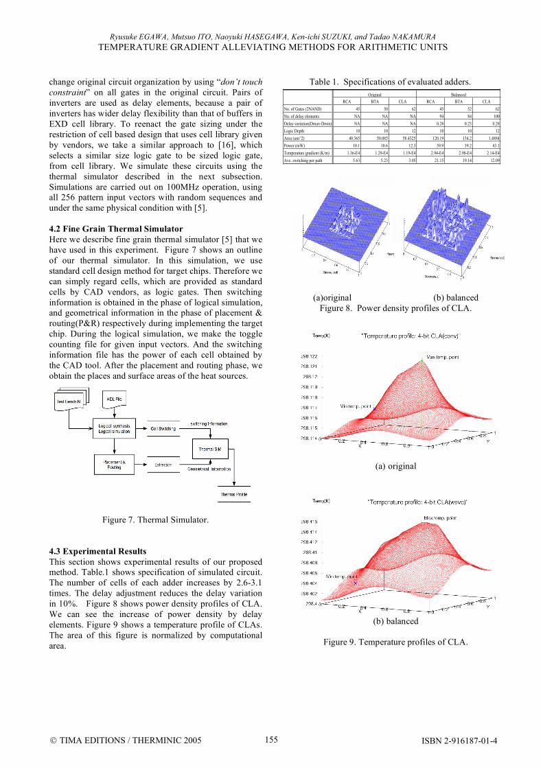
in 10%. Figure 8 shows power density profiles of CLA.
We can see the increase of power density by delay
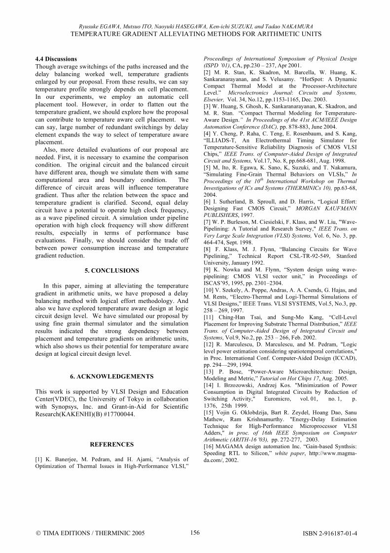
elements. Figure 9 shows a temperature profile of CLAs.
The area of this figure is normalized by computational
area.
Table 1. Specifications of evaluated adders.
(a)original (b) balanced
Figure 8. Power density profiles of CLA.
(a) original
(b) balanced
Figure 9. Temperature profiles of CLA.
RCA BTA CLA RCA BTA CLA
No. of Gates (2NAND) 45 50 62 45 52 62
No. of delay elements NA NA NA 94 84 100
Delay variation(Dmax-Dmin) NA NA NA 0.28 0.23 0.28
Logic Depth 10 10 12 10 10 12
Area (um^2) 40.365 50.085 58.4325 120.19 134.2 1.4884
Power (mW) 10.1 10.6 12.3 39.9 39.2 43.1
Temperature gradient (K/m) 1.36-E4 1.29-E4 1.19-E4 2.94-E4 2.98-E4 2.14-E4
Ave. switching per path 5.63 5.23 3.05 21.15 19.14 12.09
Original Balanced
TIMA EDITIONS / THERMINIC 2005 ISBN 2-916187-01-4 155
Ryusuke EGAWA, Mutsuo ITO, Naoyuki HASEGAWA, Ken-ichi SUZUKI, and Tadao NAKAMURA
TEMPERATURE GRADIENT ALLEVIATING METHODS FOR ARITHMETIC UNITS
4.4 Discussions
Though average switchings of the paths increased and the
delay balancing worked well, temperature gradients
enlarged by our proposal. From these results, we can say
temperature profile strongly depends on cell placement.
In our experiments, we employ an automatic cell
placement tool. However, in order to flatten out the
temperature gradient, we should explore how the proposal
can contribute to temperature aware cell placement. we
can say, large number of redundant switchings by delay
element expands the way to select of temperature aware
placement.
Also, more detailed evaluations of our proposal are
needed. First, it is necessary to examine the comparison
condition. The original circuit and the balanced circuit
have different area, though we simulate them with same
computational area and boundary condition. The
difference of circuit areas will influence temperature
gradient. Thus after the relation between the space and
temperature gradient is clarified. Second, equal delay
circuit have a potential to operate high clock frequency,
as a wave pipelined circuit. A simulation under pipeline
operation with high clock frequency will show different
results, especially in terms of performance base
evaluations. Finally, we should consider the trade off
between power consumption increase and temperature
gradient reduction.
5. CONCLUSIONS
In this paper, aiming at alleviating the temperature
gradient in arithmetic units, we have proposed a delay
balancing method with logical effort methodology. And
also we have explored temperature aware design at logic
circuit design level. We have simulated our proposal by
using fine grain thermal simulator and the simulation
results indicated the strong dependency between
placement and temperature gradients on arithmetic units,
which also shows us their potential for temperature aware
design at logical circuit design level.
6. ACKNOWLEDGEMENTS
This work is supported by VLSI Design and Education
Center(VDEC), the University of Tokyo in collaboration
with Synopsys, Inc. and Grant-in-Aid for Scientific
Research(KAKENHI)(B) #17700044.
REFERENCES
[1] K. Banerjee, M. Pedram, and H. Ajami, “Analysis of
Optimization of Thermal Issues in High-Performance VLSI,”
Proceedings of International Symposium of Physical Design
(ISPD ’01), CA, pp.230 – 237, Apr 2001.
[2] M. R. Stan, K. Skadron, M. Barcella, W. Huang, K.
Sankaranarayanan, and S. Velusamy. “HotSpot: A Dynamic
Compact Thermal Model at the Processor-Architecture
Level.” Microelectronics Journal: Circuits and Systems,
Elsevier, Vol. 34, No.12, pp.1153-1165, Dec. 2003.
[3] W. Huang, S. Ghosh, K. Sankaranarayanan, K. Skadron, and
M. R. Stan. “Compact Thermal Modeling for Temperature-
Aware Design.” In Proceedings of the 41st ACM/IEEE Design
Automation Conference (DAC), pp. 878-883, June 2004.
[4] Y. Cheng, P. Raha, C. Teng, E. Rosenbaum, and S. Kang,
“ILLIADS-T, An Electrothermal Timing Simulator for
Temperature-Sensitive Reliability Diagnosis of CMOS VLSI
Chips,” IEEE Trans. of Computer-Aided Design of Integrated
Circuit and Systems, Vol.17, No. 8, pp.668-681, Aug. 1998.
[5] M, Ito, R. Egawa, K. Sano, K, Suzuki, and T. Nakamura,
“Simulating Fine-Grain Thermal Behaviors on VLSIs,” In
Proceedings of the 10th
International Workshop on Thermal
Investigations of ICs and Systems (THERMINICs 10), pp.63-68,
2004.
[6] I. Sutherland, B. Sproull, and D. Harris, “Logical Effort:
Designing Fast CMOS Circuit,” MORGAN KAUFMANN
PUBLISHERS, 1997.
[7] W. P. Burleson, M. Ciesielski, F. Klass, and W. Liu, "Wave-
Pipelining: A Tutorial and Research Survey," IEEE Trans. on
Very Large Scale Integration (VLSI) Systems, Vol. 6, No. 3, pp.
464-474, Sept. 1998.
[8] F. Klass, M. J. Flynn, “Balancing Circuits for Wave
Pipelining,” Technical Report CSL-TR-92-549, Stanford
University, January 1992.
[9] K. Nowka and M. Flynn, “System design using wave-
pipelining: CMOS VLSI vector unit,” in Proceedings of
ISCAS’95, 1995, pp. 2301–2304.
[10] V. Szekely, A. Poppe, Andras, A. A. Csends, G. Hajas, and
M. Rents, “Electro-Thermal and Logi-Thermal Simulations of
VLSI Designs,” IEEE Trans. VLSI SYSTEMS, Vol.5, No.3, pp.
258 – 269, 1997.
[11] Ching-Han Tsai, and Sung-Mo Kang, “Cell-Level
Placement for Improving Substrate Thermal Distribution,” IEEE
Trans. of Computer-Aided Design of Integrated Circuit and
Systems, Vol.9, No.2, pp. 253 – 266, Feb. 2002.
[12] R. Marculescu, D. Marculescu, and M. Pedram, "Logic
level power estimation considering spatiotemporal correlations,"
in Proc. International Conf. Computer-Aided Design (ICCAD),
pp. 294—299, 1994.
[13] P. Bose, “Power-Aware Microarchitecture: Design,
Modeling and Metric,” Tutorial on Hot Chips 17, Aug. 2005.
[14] I. Brzozowski, Andrzej Kos. "Minimization of Power
Consumption in Digital Integrated Circuits by Reduction of
Switching Activity," Euromicro, vol. 01, no. 1, p.
1376, 25th 1999.
[15] Vojin G. Oklobdzija, Bart R. Zeydel, Hoang Dao, Sanu
Mathew, Ram Krishnamurthy. "Energy-Delay Estimation
Technique for High-Performance Microprocessor VLSI
Adders," in proc. of 16th IEEE Symposium on Computer
Arithmetic (ARITH-16 '03), pp. 272-277, 2003.
[16] MAGAMA design automation Inc. “Gain-based Synthsis:
Speeding RTL to Silicon,” white paper, http://www.magma-
da.com/, 2002.
TIMA EDITIONS / THERMINIC 2005 ISBN 2-916187-01-4 156