Temperature Dependent Current-Voltage and Capacitance ... · of an Au/n-Type Si Schottky Barrier...
7
Temperature Dependent Current-Voltage and Capacitance-Voltage Characteristics of an Au/n-Type Si Schottky Barrier Diode Modified Using a PEDOT:PSS Interlayer Zagarzusem Khurelbaatar 1 , Kyu-Hwan Shim 1 , Jaehee Cho 1 , Hyobong Hong 2 , V. Rajagopal Reddy 3,+ and Chel-Jong Choi 1,+ 1 School of Semiconductor and Chemical Engineering, Semiconductor Physics Research Center (SPRC), Chonbuk National University, Jeonju 561-756, Republic of Korea 2 IT Convergence Technology Research Laboratory, Electronics & Telecommunication Research Institute, Daejeon 306-700, Republic of Korea 3 Department of Physics, Sri Venkateswara University, Tirupati-517 502, India The temperature dependence of the current-voltage (I-V) and capacitance-voltage (C-V) characteristics of an Au/n-type Si Schottky barrier diode (SBD) with a PEDOT:PSS interlayer was investigated. The SBD parameters, such as Schottky barrier height () B ), ideality factor (n), saturation current (I 0 ), doping concentration (N D ), and series resistance (R s ), were obtained as a function of temperature. The Richardson constant (A**) obtained from the In(I o /T 2 ) versus 1000/T plot was much less than the theoretical value for n-Si. The mean Schottky barrier height ( bo ) and standard deviation (· 0 ) calculated using the apparent Schottky barrier height () ap ) versus 1/2kT plot were 1.26 eV and 0.15 eV, respectively. From a fit of the modified Richardson plot of ln(I 0 /T 2 ) ¹ (q·) 2 /2(kT) 2 versus 1000/T , the A** was extracted as 134 A/cm 2 K 2 , which was close to the theoretical value of the n-Si. The interface state densities obtained from the Au/PEDOT:PSS/n-Si SBD decreased with increasing temperature. Furthermore, the conduction mechanism dominating the reverse-bias leakage current in Au/PEDOT:PSS/n-Si SBD was described and discussed. [doi:10.2320/matertrans.M2014263] (Received July 14, 2014; Accepted October 6, 2014; Published November 14, 2014) Keywords: Schottky barrier diode, poly(3,4-ethylenedioxythiophene):polystyrene sulfonate (PEDOT:PSS), gaussian distribution, barrier inhomogeneity 1. Introduction Schottky barrier diodes (SBDs) have received significant attention in the development of various electronic devices due to their low forward voltage drop and fast switching action. There are numerous reports on the theoretical and experimental studies of SBDs, but they continue to be extensively studied to fully understand the nature of the contact. The fabrication of high quality SBDs with a low ideality factor (n) using a thin interfacial layer is one of the essential prerequisites for electronic devices. Recent research has been performed by applying conducting polymer materials to SBDs as an interfacial layer by a solution based spin-coating process. 1-3) It is found that performance, reliability and stability of SBDs depends on various parame- ters such as the fabrication process, surface preparation, density of surface states distributed at the interface, device temperature and voltage, series resistance (R S ) of the device, thermal and mechanical stability of the polymer used. Among various conducting polymers, poly(3,4-ethylenedioxythio- phene):poly (styrene sulfonate) (PEDOT:PSS), one of the most important polymers, has recently received considerable interest because it exhibits a p-type semiconductor with a high work function (³ 5 eV), high conductivity (35-300 S·cm ¹1 at room temperature), good transparency (³95% at visible region), excellent photo-stability, and good environ- mental stability. 4,5) Several research groups have used PEDOT:PSS as a Schottky junction with n-type Si sub- strates. 6-10) According to previous reports, the electrical transport properties of SBDs depend highly on the conditions of the fabrication processes, such as the utilization of a particular solvent, the amount of PSS, the doping ratio of PEDOT in the PEDOT:PSS mixture, the uniformity of the PEDOT:PSS thin film, and the environmental conditions during the fabrication. As a result, there is a large variation in the electrical transport of PEDOT:PSS/n-Si SBDs. More- over, there is no experimental study done on their temper- ature-dependent electrical characteristics. Analysis of the current-voltage (I-V) and capacitance-voltage (C-V) charac- teristics of metal-semiconductor and metal-insulator-semi- conductor structures only at room temperature cannot provide detailed information regarding the current conduction mechanisms or the nature of the barrier formation at the metal-semiconductor interface. 11) On the other hand, the temperature dependence of the I-V and C-V characteristics could allow us to gain insight into different aspects of characteristics such as nature of interfacial insulator layer and carrier conduction mechanism. In this study, we fabricated Au/n-type Si SBDs with a PEDOT:PSS interlayer using spin-coating process and reactive ion etching process (RIE). For the electrical characteristics of the Au/PEDOT:PSS/n-Si SBDs, electrical transport measurement were investigated by both I-V and C-V measurements in the temperature range from 200 to 400 K. The Schottky barrier height () B ), n, saturation current (I 0 ), doping concentration (N D ), and R S of Au/PEDOT:PSS/n-Si SBDs were extracted at different temperatures. The temper- ature dependence of the energy distribution of the interface state density (N SS ) profile was determined based on the variation of the ideality factor with forward bias and temperature. Temperature-dependent barrier characteristics of the Au/PEDOT:PSS/n-Si SBDs were also interpreted based on the existence of the Gaussian distribution of the + Corresponding author, E-mail: reddy_vrg@rediffmail.com, cjchoi@jbnu. ac.kr Materials Transactions, Vol. 56, No. 1 (2015) pp. 10 to 16 © 2014 The Japan Institute of Metals and Materials
-
Upload
truongminh -
Category
Documents
-
view
214 -
download
0
Transcript of Temperature Dependent Current-Voltage and Capacitance ... · of an Au/n-Type Si Schottky Barrier...

Temperature Dependent Current-Voltage and Capacitance-Voltage Characteristicsof an Au/n-Type Si Schottky Barrier Diode Modified Using a PEDOT:PSS Interlayer
Zagarzusem Khurelbaatar1, Kyu-Hwan Shim1, Jaehee Cho1, Hyobong Hong2,V. Rajagopal Reddy3,+ and Chel-Jong Choi1,+
1School of Semiconductor and Chemical Engineering, Semiconductor Physics Research Center (SPRC),Chonbuk National University, Jeonju 561-756, Republic of Korea2IT Convergence Technology Research Laboratory, Electronics & Telecommunication Research Institute,Daejeon 306-700, Republic of Korea3Department of Physics, Sri Venkateswara University, Tirupati-517 502, India
The temperature dependence of the current-voltage (I-V) and capacitance-voltage (C-V) characteristics of an Au/n-type Si Schottky barrierdiode (SBD) with a PEDOT:PSS interlayer was investigated. The SBD parameters, such as Schottky barrier height ()B), ideality factor (n),saturation current (I0), doping concentration (ND), and series resistance (Rs), were obtained as a function of temperature. The Richardson constant(A**) obtained from the In(Io/T 2) versus 1000/T plot was much less than the theoretical value for n-Si. The mean Schottky barrier height ( ��bo)and standard deviation (·0) calculated using the apparent Schottky barrier height ()ap) versus 1/2kT plot were 1.26 eV and 0.15 eV, respectively.From a fit of the modified Richardson plot of ln(I0/T 2) ¹ (q·)2/2(kT)2 versus 1000/T, the A** was extracted as 134A/cm2K2, which was closeto the theoretical value of the n-Si. The interface state densities obtained from the Au/PEDOT:PSS/n-Si SBD decreased with increasingtemperature. Furthermore, the conduction mechanism dominating the reverse-bias leakage current in Au/PEDOT:PSS/n-Si SBD was describedand discussed. [doi:10.2320/matertrans.M2014263]
(Received July 14, 2014; Accepted October 6, 2014; Published November 14, 2014)
Keywords: Schottky barrier diode, poly(3,4-ethylenedioxythiophene):polystyrene sulfonate (PEDOT:PSS), gaussian distribution, barrierinhomogeneity
1. Introduction
Schottky barrier diodes (SBDs) have received significantattention in the development of various electronic devicesdue to their low forward voltage drop and fast switchingaction. There are numerous reports on the theoretical andexperimental studies of SBDs, but they continue to beextensively studied to fully understand the nature of thecontact. The fabrication of high quality SBDs with a lowideality factor (n) using a thin interfacial layer is one of theessential prerequisites for electronic devices. Recent researchhas been performed by applying conducting polymermaterials to SBDs as an interfacial layer by a solution basedspin-coating process.13) It is found that performance,reliability and stability of SBDs depends on various parame-ters such as the fabrication process, surface preparation,density of surface states distributed at the interface, devicetemperature and voltage, series resistance (RS) of the device,thermal and mechanical stability of the polymer used. Amongvarious conducting polymers, poly(3,4-ethylenedioxythio-phene):poly (styrene sulfonate) (PEDOT:PSS), one of themost important polymers, has recently received considerableinterest because it exhibits a p-type semiconductor with ahigh work function (³ 5 eV), high conductivity (35300S·cm¹1 at room temperature), good transparency (³95% atvisible region), excellent photo-stability, and good environ-mental stability.4,5) Several research groups have usedPEDOT:PSS as a Schottky junction with n-type Si sub-strates.610) According to previous reports, the electricaltransport properties of SBDs depend highly on the conditions
of the fabrication processes, such as the utilization of aparticular solvent, the amount of PSS, the doping ratio ofPEDOT in the PEDOT:PSS mixture, the uniformity of thePEDOT:PSS thin film, and the environmental conditionsduring the fabrication. As a result, there is a large variation inthe electrical transport of PEDOT:PSS/n-Si SBDs. More-over, there is no experimental study done on their temper-ature-dependent electrical characteristics. Analysis of thecurrent-voltage (I-V) and capacitance-voltage (C-V) charac-teristics of metal-semiconductor and metal-insulator-semi-conductor structures only at room temperature cannot providedetailed information regarding the current conductionmechanisms or the nature of the barrier formation at themetal-semiconductor interface.11) On the other hand, thetemperature dependence of the I-V and C-V characteristicscould allow us to gain insight into different aspects ofcharacteristics such as nature of interfacial insulator layer andcarrier conduction mechanism.
In this study, we fabricated Au/n-type Si SBDs witha PEDOT:PSS interlayer using spin-coating process andreactive ion etching process (RIE). For the electricalcharacteristics of the Au/PEDOT:PSS/n-Si SBDs, electricaltransport measurement were investigated by both I-V and C-Vmeasurements in the temperature range from 200 to 400K.The Schottky barrier height ()B), n, saturation current (I0),doping concentration (ND), and RS of Au/PEDOT:PSS/n-SiSBDs were extracted at different temperatures. The temper-ature dependence of the energy distribution of the interfacestate density (NSS) profile was determined based on thevariation of the ideality factor with forward bias andtemperature. Temperature-dependent barrier characteristicsof the Au/PEDOT:PSS/n-Si SBDs were also interpretedbased on the existence of the Gaussian distribution of the
+Corresponding author, E-mail: [email protected], [email protected]
Materials Transactions, Vol. 56, No. 1 (2015) pp. 10 to 16©2014 The Japan Institute of Metals and Materials
barrier heights. Furthermore, the possible current conductionmechanism of the Schottky contacts modified using thePEDOT:PSS interlayer was also studied.
2. Experimental Procedures
The n-type Si (100) wafers with a resistivity of 110³·cmwere used as a starting material. The carrier density of Sisubstrate, measured by Hall measurement system, wasextracted to be 1.21 © 1015 cm3. After removing nativeoxide, the PEDOT:PSS layer was spin-coated on a cleanedn-Si wafer, followed by baking at 150°C in air. The scanningelectron microscope examination (not shown here) revealedthat the thickness of the PEDOT:PSS film was approximately60 nm. In addition, the sheet resistance of PEDOT:PSS filmspin-coated on insulating glass substrate, measured by thefour-point probe, was found to be ³2.6 © 103³/squre. Thetop Au (100 nm) electrode with 1-mm diameter (area =7.85 © 10¹3 cm2) was formed on PEDOT:PSS film with ametal mask by an e-beam evaporation system at a pressure of3.99 © 10¹4 Pa. The redundant PEDOT:PSS film was thenremoved by the O2 plasma RIE process and resulting in acircular dot shaped Au/PEDOT:PSS electrode formed on n-Si. The GaIn paste was then applied to the backside of then-Si wafer for ohmic contacts. The schematic cross sectionof the Au/PEDOT:PSS/n-Si SBD is shown in the insetof Fig. 1. The I-V and C-V measurements of the Au/PEDOT:PSS/n-Si SBD were performed using a semicon-ductor parameter analyzer (Agilent Technologies, 4155C)and LCR meter (Agilent Technologies, 4284A) at a temper-ature range of 200400K in steps of 40K under a darkcondition.
3. Results and Discussion
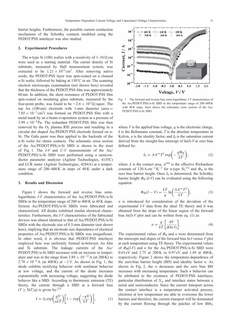
Figure 1 shows the forward and reverse bias semi-logarithmic I-V characteristics of the Au/PEDOT:PSS/n-SiSBDs in the temperature range of 200 to 400K in 40K steps.Sixteen Au/PEDOT:PSS/n-Si SBDs were fabricated andcharacterized. All diodes exhibited similar electrical charac-teristics. Furthermore, the I-V characteristics of the fabricateddevices was almost identical to that of Au/PEDOT:PSS/n-SiSBDs with the electrode size of 0.5-mm diameter (not shownhere), implying that an electrode size dependence of electricalproperties of Au/PEDOT:PSS/n-Si SBDs was insignificant.In other word, it is obvious that PEDOT:PSS interlayeremployed here was uniformly formed in-between Au filmand Si substrate. The leakage currents of the Au/PEDOT:PSS/n-Si SBD increases with an increase in temper-ature and was in the range from 3.89 © 10¹12A (at 200K) to2.78 © 10¹6 A (at 400K) at ¹1V. As shown in Fig. 1, thediode exhibits rectifying behavior with nonlinear behaviorat low voltage, and the current of the diode increasesexponentially with increasing voltage, suggesting the diodebehaves like a SBD. According to thermionic emission (TE)theory, the current through a SBD at a forward bias(V ² 3kT/q) is given by:12)
I ¼ I0 expqV
nkT
� �1� exp
�qV
kT
� �� �; ð1Þ
where V is the applied bias voltage, q is the electronic charge,k is the Boltzmann constant, T is the absolute temperature inKelvin, n is the ideality factor, and I0 is the saturation currentderived from the straight-line intercept of ln(I)-V at zero biasdefined by:
I0 ¼ AA��T 2 exp � q�B
kT
� �; ð2Þ
where A is the contact area, A** is the effective Richardsonconstant of 120A cm¹2 K¹2 for n-type Si,13) and )B is thezero bias barrier height. Once I0 is determined, the Schottkybarrier height )B (I-V) can be evaluated using the followingequation:
�BðI � V Þ ¼ kT
qln
AA��T 2
kT
� �; ð3Þ
n is introduced for consideration of the deviation of theexperimental I-V data from the ideal TE theory and it wasobtained from the slope of the linear region of the forwardbias ln(I)-V plot and can be written from eq. (1) as:
n ¼ q
kT
dV
dðln IÞ
� �; ð4Þ
The experimental values of )B and n were determined fromthe intercepts and slopes of the forward bias ln I versus V plotat each temperature using TE theory. The experimental valuesof )B(I-V) and n for the Au/PEDOT:PSS/n-Si SBD were0.63 eV and 2.75 at 200K to 0.97 eV and 1.49 at 400K,respectively. Figure 2 shows the temperature-dependence ofthe zero-bias barrier height (BH) and ideality factor n. Asshown in Fig. 2, the n decreases and the zero bias BHincreases with increasing temperature. Such n behavior canbe attributed to the existence of PEDOT:PSS interlayer,particular distribution of Nss and interface states between ametal and semiconductor. Since the current transport acrossthe contact interface is a temperature activated process,electrons at low temperature are able to overcome the lowerbarriers and therefore, the current transport will be dominatedby the current flowing through the patches of low BHs,
Fig. 1 The forward and reverse bias semi-logarithmic I-V characteristics ofthe Au/PEDOT:PSS/n-Si SBD in the temperature range of 200400Kwith 40K steps. Inset shows the schematic cross section of the Au/PEDOT:PSS/n-Si SBD.
Temperature Dependent Current-Voltage and Capacitance-Voltage Characteristics 11

leading to a larger n. However, as the temperature increases,more electrons have sufficient energy to overcome the BH.An apparent increase in the n and a decrease in the BH at lowtemperatures are possibly caused by other effects such asthickness inhomogeneities and non-uniformity of the inter-facial charges.
Furthermore, the Au/PEDOT:PSS/n-Si SBD shows a non-ideal I-V behavior with a large ideality factor, which may bedue to the presence of the PEDOT:PSS interlayer. There arevarious parameters that cause deviations in ideal behaviorincluding RS and the presence of an interfacial layer.14)
Therefore, RS of the Au/PEDOT:PSS/n-Si SBD is extractedusing a method developed by Cheung and Cheun14) at ahigher current range. The calculated Rs from the plot ofdV/d(ln I) versus I (not shown) were 114.1³ at 200K and24³ at 400K for the Au/PEDOT:PSS/n-Si SBD. The RS
estimated from the plot of H (I) versus I was 145³ at 200Kand 32.1³ at 400K. The Rs calculated from the dV/d(ln I)versus I plot are in good agreement with those estimated fromthe H(I) versus I plot, implying their consistency and validity.Experimental results reveal that Rs increases with decreasingtemperature. The increase of RS with a decrease in temper-ature was due to factors responsible for an increase in n andthe lack of free carriers at low temperatures.
Conventional TE theory is typically used to determine theBH. Alternatively, there have been several reports deviatingfrom this classical TE theory. The Richardson plot is drawnto obtain the BH in another way. Equation (2) can berewritten as:
lnI0T 2
� �¼ lnðAA��Þ � q�bo
kT; ð5Þ
The conventional Richardson plot of ln(Io/T 2) versus 103/Tis shown in Fig. 3. The temperature dependence of theexperimental ln(Io/T 2) versus 103/T plot produces a straightline. The activation energy and Richardson constant wereobtained from the slope and intercept of this straight line as0.27 eV and 1.98 © 10¹7A/cm2K2, respectively. The exper-imentally-obtained Richardson constant value was much lessthan the theoretical Richardson constant value for n-Si. Sucha large discrepancy between the experimental and theoreticalvalues of the Richardson constant could be attributed to thecalculation using the temperature-dependent I-V character-istics, which may be affected by the lateral inhomogeneity of
the BH and potential fluctuations due to the PEDOT:PSSinterlayer.
In order to explain the abnormal deviations of the I-Vcharacteristics of the SBD from classical TE theory, thelateral distribution of BH was adopted with a Gaussiandistribution. The Gaussian distribution of the BH with a meanvalue Schottky barrier height ( ��bo) and a standard deviation(·o) yields the following expression for the BH:15)
�ap ¼ �boðT ¼ 0Þ � q·20
2kT; ð6Þ
where )ap is the apparent Schottky barrier height and ·0 is thestandard deviation of the )B distribution that is typicallysufficiently small to be neglected. The observed variation of nwith temperature in the model is given by:15)
1
nap� 1
� �¼ μ2 �
qμ32kT
; ð7Þ
where nap is the apparent ideality factor, μ2 and μ3 quantifythe voltage deformation of the barrier height distribution,which may depend on temperature. Gaussian distributionmay cause the decrease of zero bias BH and the influence isdetermined by the standard deviation. As shown in Fig. 4,��bo and ·0, which correspond to the y-axis intercept and theslope of the linear fit to the plots of )ap as a function of1/2kT, were estimated as 1.26 eVand 0.15 eV, respectively. ·0is a general measure of the homogeneity of the Schottkybarrier, with a lower ·0 value corresponding to a more
Fig. 2 Temperature dependence of )B and n obtained from forward biasI-V characteristics for Au/PEDOT:PSS/n-Si in the range of 200400K.
Fig. 3 Richardson plots of the In (I0/T 2) versus 1000/T for the Au/PEDOT:PSS/n-Si SBD in the range of 200400K.
Fig. 4 The zero bias barrier height ()ap) versus 1/2kT curves of the Au/PEDOT:PSS SBD according to Gaussian distribution of the barrier height.
Z. Khurelbaatar et al.12
homogeneous BH. Nevertheless, this inhomogeneity andpotential fluctuation dramatically affects the low temperatureI-V characteristics. As compared to ��boðT ¼ 0Þ ¼ 1:26 eV,the ·0 = 0.15 eV is not small, implying Schottky barrierinhomogeneity in the studied SBD. As previously shown,15)
barrier inhomogeneities can occur as a result of inhomoge-neities in the composition of the interfacial layer, non-uniformity of interfacial charges and interfacial layer thick-ness. Therefore, low temperature I-V characteristics areaffected by this inhomogeneity and potential fluctuation.
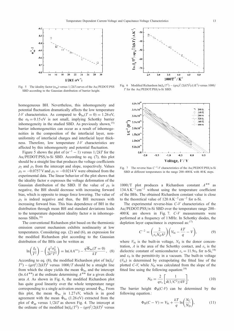
Figure 5 shows the plot of (n¹1 ¹ 1) versus 1/2kT for theAu/PEDOT:PSS/n-Si SBD. According to eq. (7), this plotshould be a straight line that produces the voltage coefficientsμ2 and μ3 from the intercept and slope, respectively. Valuesμ2 = ¹0.0757V and μ3 = ¹0.0214V were obtained from theexperimental data. The linear behavior of the plot shows thatthe ideality factor n expresses the voltage deformation of theGaussian distribution of the SBD. If the value of μ2 isnegative, the BH should decrease with increasing forwardbias, which is opposite to image force lowering. The value ofμ3 is indeed negative and thus, the BH increases withincreasing forward bias. This bias dependence of BH in thedistribution through mean BH and standard deviations leadsto the temperature dependent ideality factor n in inhomoge-neous SBDs.16)
The conventional Richardson plot based on the thermionicemission current mechanism exhibits nonlinearity at lowtemperatures. Considering eqs. (2) and (6), an expression forthe modified Richardson plot according to the Gaussiandistribution of the BHs can be written as
lnI0T 2
� �� q2·2
0
2k2T 2
� �¼ lnðAA��Þ � q�boðT ¼ 0Þ
kT; ð8Þ
According to eq. (8), the modified Richardson plot of ln(I0/T 2) ¹ (q·)2/2(kT)2 versus 1000/T should be a straight linefrom which the slope yields the mean ��bo and the intercept(lnAA**) at the ordinate determining A** for a given diodearea A. As shown in Fig. 6, the modified Richardson plothas quite good linearity over the whole temperature rangecorresponding to a single activation energy around ��bo. Fromthis plot, the mean ��bo is 1.27 eV, which is in goodagreement with the mean ��bo (1.26 eV) extracted from theplot of )ap versus 1/2kT as shown Fig. 4. The intercept atthe ordinate of the modified ln(I0/T 2) ¹ (q·)2/2(kT)2 versus
1000/T plot produces a Richardson constant A** as134AK¹2 cm¹2 without using the temperature coefficientof the BHs. The obtained Richardson constant value is closeto the theoretical value of 120AK¹2 cm¹2 for n-Si.
The experimental reverse-bias C-V characteristics of theAu/PEDOT:PSS/n-Si SBD over the temperature range 200400K are shown in Fig. 7. C-V measurements wereperformed at a frequency of 1MHz. In Schottky diodes, thedepletion layer capacitance is expressed as:17)
C�2 ¼ 2
¾sNdA2
� �Vbi �
kT
q� V
� �; ð9Þ
where Vbi is the built-in voltage, Nd is the donor concen-tration, A is the area of the Schottky contact, and ¾s is thedielectric constant of semiconductor ¾s = 11.9¾0 for n-Si,18)
and ¾0 is the permittivity in a vacuum. The built-in voltage(Vbi) is determined by extrapolating the fitted line of theplotted C-V, while ND was calculated from the slope of thefitted line using the following equation:19)
ND ¼ 2
q¾s
1
dð1=C2Þ=dV
� �; ð10Þ
The barrier height )B(C-V) can be determined by thefollowing equation.:
�BðC� V Þ ¼ Vbi þkT
qln
NC
ND
� �; ð11Þ
Fig. 5 The ideality factor (nap) versus 1/2kT curves of the Au/PEDOT:PSSSBD according to the Gaussian distribution of barrier height.
Fig. 6 Modified Richardson ln(I0/T 2) ¹ (q·0)2/2(kT)2(A/K2) versus 1000/T for the Au/PEDOT:PSS/n-Si SBD.
Fig. 7 The reverse bias C¹2-V characteristics of the Au/PEDOT:PSS/n-SiSBD at different temperatures in the range 200400K with 40K steps.
Temperature Dependent Current-Voltage and Capacitance-Voltage Characteristics 13
with NC ¼ 2ð2m�kT Þ3=2
h3; ð12Þ
where ND is the donor concentration and NC is the effectivedensity of states in the Si conduction band edge, m* =1.08m0 is the effective mass of electrons in Si and m0 is therest mass of the electron.20) The ND and )B(C-V) for the Au/PEDOT:PSS/n-Si SBD can be calculated from eq. (10) andeq. (11), respectively. The values of )B(C-V) are given inTable 1. The barrier height values obtained from the reversebias C¹2-V characteristics varied from 0.85 eV at 200K to0.69 eV at 400K, illustrating )B(C-V) increases withdecreasing temperature. The calculated values of ND variedfrom 1.32 © 1015 cm¹3 at 200K to 1.41 © 1015 cm¹3 at400K. As shown in Table 1, the donor concentration of then-Si slightly increases as the temperature increases. At lowtemperatures, mostly all of the impurities were frozen out,causing a strong increase in the RS of the diode, which makesthe measured capacitance appear smaller. More electrons maybe frozen at the donor level in the freeze-out region andconduction mechanisms in the freeze-out regions arecomplex. Since the donor concentration increases, then thecapacitance also increases with increasing temperature.
Additionally, the barrier heights obtained from C-Vmeasurements were greater than those obtained from I-Vmeasurements. The discrepancy between )B(C-V) and)B(I-V) can be attributed to the characteristic nature of theC-V and I-V measurement techniques, and the existence of aninterfacial dipole layer or trap states at the PEDOT:PSS/n-Siinterface. Additionally, the discrepancy between )B(C-V) and)B(I-V) can be explained by the excess capacitance and SBHinhomogeneities.21) The current in the I-V measurement isdominated by the current that flows through the region of lowSBH. Thus, the measured )B(I-V) is significantly less thanthe weighed arithmetic average of the SBHs. Alternatively,the barrier height determined from the C-V or flat band wasinfluenced by the distribution of charge at the depletionregion boundary, which follows the weighted arithmeticaverage of the SBHs. Consequently, the SBH calculated fromthe zero-bias intercept assuming TE as a current transportmechanism is well below the C-V or flat-band measured BHand the weighted arithmetic average of SBHs. Furthermore,the capacitance C is insensitive to potential fluctuations on alength scale less than the space charge region and the C-Vmeasurement probes the average junction capacitance at the
interface, thereby yielding an average value for the barrierheight distribution, while the I-V measurement produces aminimum value for the barrier height.22)
The NSS for the Au/PEDOT:PSS/n-Si SBD can beobtained from the forward bias I-V data by taking thevoltage-dependent ideality factor nðV; T Þ with the effectivebarrier height �bðV; T Þ. The parameters of nðV; T Þ and )b
(V, T) can be estimated from the following equations:23)
nðV Þ ¼ q
kT
V
lnðI=IoÞ
� �¼ 1þ ¤
¾i
¾S
WD
þ qNSS
� �ð13Þ
�bðV; T Þ ¼ �IVbo þ ¢V ¼ �IV
bo þ 1� 1
nðV; T Þ
� �ð14Þ
where WD is the space charge region width, ¤ is the thicknessof the interfacial organic layer, ¾i and ¾S are the permitivitiesof the interfacial layer and semiconductor, and ¢(= d)eff/dV = 1 ¹ 1/n(V)) is the change in effective BH with biasvoltage. As proposed by Card and Rhoderick,23) in interfacestates in equilibrium with the semiconductor, the idealityfactor becomes greater than unity and the NSS is given by:
NSSðV Þ ¼1
q
¾i
¤ðnðV; T Þ � 1Þ � ¾S
WD
� �: ð15Þ
Additionally, in n-type semiconductors, the energy interfacestates with respect to the conduction band edge (EC-ESS) areobtained as:
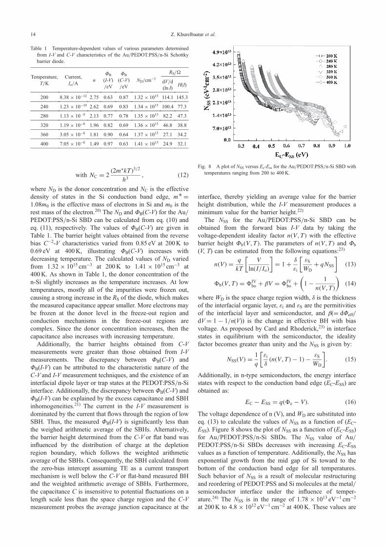
EC � ESS ¼ qð�e � V Þ: ð16ÞThe voltage dependence of n (V), and WD are substituted intoeq. (13) to calculate the values of NSS as a function of (EC-ESS). Figure 8 shows the plot of NSS as a function of (EC-ESS)for Au/PEDOT:PSS/n-Si SBDs. The NSS value of Au/PEDOT:PSS/n-Si SBDs decreases with increasing EC-ESS
values as a function of temperature. Additionally, the NSS hasexponential growth from the mid gap of Si toward to thebottom of the conduction band edge for all temperatures.Such behavior of NSS is a result of molecular restructuringand reordering of PEDOT:PSS and Si molecules at the metal/semiconductor interface under the influence of temper-ature.24) The NSS is in the range of 1.78 © 1013 eV¹1 cm¹2
at 200K to 4.8 © 1012 eV¹1 cm¹2 at 400K. These values are
Table 1 Temperature-dependent values of various parameters determinedfrom I-V and C-V characteristics of the Au/PEDOT:PSS/n-Si Schottkybarrier diode.
Temperature,T/K
Current,Io/A
n)B
(I-V)/eV
)B
(C-V)/eV
ND/cm¹3
RS/³
dV/d(ln I)
H(I)
200 8.38 © 10¹12 2.75 0.63 0.87 1.32 © 1015 114.1 145.3
240 1.23 © 10¹10 2.62 0.69 0.83 1.34 © 1015 100.4 77.3
280 1.13 © 10¹9 2.13 0.77 0.78 1.35 © 1015 82.2 47.3
320 1.19 © 10¹8 1.96 0.82 0.69 1.36 © 1015 46.8 38.8
360 3.05 © 10¹8 1.81 0.90 0.64 1.37 © 1015 27.1 34.2
400 7.05 © 10¹8 1.49 0.97 0.63 1.41 © 1015 24.9 32.1
Fig. 8 A plot of NSS versus Ec-Ess for the Au/PEDOT:PSS/n-Si SBD withtemperatures ranging from 200 to 400K.
Z. Khurelbaatar et al.14
similar to the results reported in the literature.25,26) Theinterface states and interfacial layer between the metal andsemiconductor play a significant role in the determination ofthe Schottky barrier parameters of the devices.
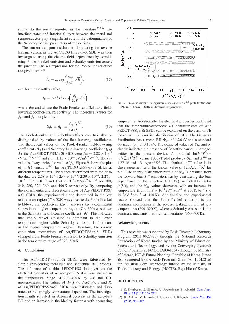
The current transport mechanism dominating the reverseleakage current in the Au/PEDOT:PSS/n-Si SBD was theninvestigated using the electric field dependence by consid-ering Poole-Frenkel emission and Schottky emission acrossthe junction. The I-V expression for the Poole-Frenkel effectare given as:27,28)
IR ¼ Io exp¢PF
kBT
ffiffiffiffiE
p� �; ð17Þ
and for the Schottky effect,
IR ¼ AA�T 2 exp¢S
kBT
ffiffiffiffiE
p� �ð18Þ
where ¢PF and ¢S are the Poole-Frenkel and Schottky field-lowering coefficients, respectively. The theoretical values for¢PF and ¢S are given by:
2¢S ¼ ¢PF ¼q3
³¾
� �1=2
: ð19Þ
The Poole-Frenkel and Schottky effects can typically bedistinguished by values of the field-lowering coefficients.The theoretical values of the Poole-Frenkel field-loweringcoefficient (¢PF) and Schottky field-lowering coefficient (¢S)for the Au/PEDOT:PSS/n-Si SBD were ¢PF = 2.22 © 10¹5
eV/m1/2 V¹1/2 and ¢S = 1.11 © 10¹5 eV/m1/2 V¹1/2. The ¢PFvalue is always twice the value of ¢S. Figure 9 shows the plotof ln(IR) versus E1/2 for Au/PEDOT:PSS/n-Si SBDs atdifferent temperatures. The slopes determined from the fit tothe data are 2.58 © 10¹5, 2.44 © 10¹5, 2.39 © 10¹5, 2.28 ©10¹5, 1.25 © 10¹5 and 1.24 © 10¹5 eV/m1/2 V¹1/2 for 200,240, 280, 320, 360, and 400K respectively. By comparingthe experimental and theoretical slopes of Au/PEDOT:PSS/n-Si SBDs, the experimental slope determined in the lowtemperature region (T < 320) was closer to the Poole-Frenkelfield-lowering coefficient (¢PF), whereas the experimentalslopes in the higher temperature region (T > 320) was closerto the Schottky field-lowering coefficient (¢S). This indicatesthat Poole-Frenkel emission is dominant in the lowertemperature region while Schottky emission is dominantin the higher temperature region. Therefore, the currentconduction mechanism of Au/PEDOT:PSS/n-Si SBDschanged from Poole-Frenkel emission to Schottky emissionin the temperature range of 320360K.
4. Conclusions
The Au/PEDOT:PSS/n-Si SBDs were fabricated bysimple spin-coating technique and sequential RIE process.The influence of a thin PEDOT:PSS interlayer on theelectrical properties of Au/n-type Si SBDs were studied inthe temperature range of 200400K by I-V and C-Vmeasurements. The values of )B(I-V), )B(C-V), n and Rs
of Au/PEDOT:PSS/n-Si SBDs were estimated and illus-trated to be strongly temperature dependent. The investiga-tion results revealed an abnormal decrease in the zero-biasBH and an increase in the ideality factor n with decreasing
temperature. Additionally, the electrical properties confirmedthat the temperature-dependent I-V characteristics of Au/PEDOT:PSS/n-Si SBDs can be explained on the basis of TEtheory with a Gaussian distribution of BHs. The Gaussiandistribution has a mean BH ��bo of 1.26 eV and a standarddeviation (·o) of 0.15 eV. The extracted values of ��bo and ·oclearly indicates the presence of Schottky barrier inhomoge-neities in the present device. A modified lnðI0=T 2Þ �ðq2·2
0=2k2T 2Þ versus 1000/T plot produces ��bo and A** as
1.27 eV and 134A/cm2K2. The obtained A** value is inclose agreement with the known value of 120A/cm2K2 forn-Si. The energy distribution profile of NSS is obtained fromthe forward bias I-V characteristics by considering the biasdependence of the effective BH (¯e) and ideality factor(n(V)), and the NSS values decreases with an increase intemperature (from 1.78 © 1013 eV¹1 cm¹2 at 200K to 4.8 ©1012 eV¹1 cm¹2 at 400K). Additionally, the experimentalresults showed that the Poole-Frenkel emission is thedominant mechanism in the reverse leakage current at lowtemperatures (200320K), whereas Schottky emission is thedominant mechanism at high temperatures (360400K).
Acknowledgements
This research was supported by Basic Research LaboratoryProgram (2011-0027956) through the National ResearchFoundation of Korea funded by the Ministry of Education,Science and Technology, and by the Converging ResearchCenter Program (2014M3C1A8048834) through the Ministryof Science, ICT & Future Planning, Republic of Korea. It wasalso supported by the R&D Program (Grant No. 10045216)for Industrial Core Technology funded by the Ministry ofTrade, Industry and Energy (MOTIE), Republic of Korea.
REFERENCES
1) S. Demirezen, Z. Sönmez, U. Aydemir and S. Alrindal: Curr. Appl.Phys. 12 (2012) 266272.
2) K. Akkılıç, M. E. Aydın, I. Uzun and T. Kılıçoglu: Synth. Met. 156(2006) 958962.
Fig. 9 Reverse current (in logarithmic scale) versus E1/2 plots for the Au/PEDOT:PSS/n-Si SBD at different temperatures.
Temperature Dependent Current-Voltage and Capacitance-Voltage Characteristics 15

3) N. Şimşir, H. Şafak, Ö. F. Yüksel and M. Kuş: Curr. Appl. Phys. 12(2012) 15101514.
4) K. S. Kang, K. J. Han and J. Kim: IEEE Trans. Nanotechn. 8 (2009)627630.
5) W. Feng, Y. Li, J. Wu, H. Noda, A. Fujii, M. Ozaki and K. Yoshino:J. Phys. Condens. Mater. 19 (2007) 186220.
6) Z. Tang, Q. Liu, I. Khatri, R. Ishikawa, K. Ueno and H. Shirai: Phys.Status Solidi C 9 (2012) 20752078.
7) Y. Lin and Y. Su: J. Appl. Phys. 111 (2012) 073712.8) Y. Lin, B. Huang, Y. Lien, C. Lee, C. Tsai and H. Chang: J. Phys. D:
Appl. Phys. 42 (2009) 165104.9) M. Price, J. Foley, R. May and S. Maldonado: Appl. Phys. Lett. 97
(2010) 083503.10) J. Lin, J. Zeng, Y. Su and Y. Lin: Appl. Phys. Lett. 100 (2012) 153509.11) T. Tunç, I. Dökme, Ş. Altindal and I. Uslu: Optoelectron. Adv. Mater.
Rapid Commun. 4 (2010) 947950.12) V. Janardhanam, H.-K. Lee, K.-H. Shim, H.-B. Hong, S.-H. Lee, K.-S.
Ahn and C.-J. Choi: J. Alloy. Compd. 504 (2010) 146150.13) E. H. Rhoderick and R. H. Williams: Metal-Semiconductor Contacts
2nd ed., (Clarendon Press, Oxford; U.K., 1988) pp. 3841.14) S. K. Cheung and N. W. Cheung: Appl. Phys. Lett. 49 (1986) 8587.15) Y. Song, R. Van Meirhaeghe, W. Laflere and F. Cardon: Solid State
Electron. 29 (1986) 633638.16) N. Yıldırım and A. Türüt: Microelectron Eng. 86 (2009) 22702274.17) S. Chand and S. Bala: Appl. Surf. Sci. 252 (2005) 358363.18) S. Ashok, J. M. Borrego and R. J. Gutmann: Solid-State Electron. 22
(1979) 621631.19) R. T. Tung: Phys. Rev. B 45 (1992) 1350913523.20) S. Chand and J. Kumar: J. Semicond. Sci. Technol. 11 (1996) 1203
1208.21) F. Yakuphanoglu and B. F. Senkel: J. Phys. Chem. C 111 (2007) 1840
1846.22) Ö. Güllü, O. Baris, M. Biber and A. Türüt: Appl. Surf. Sci. 254 (2008)
30393044.23) H. C. Card and E. H. Rhoderick: J. Phys. D: Appl. Phys. 4 (1971)
15891601.24) B. Akkal, Z. Benamara, A. Boudissa, N. B. Bouiadjra, M. Amrani, I.
Bideux and B. Gruzza: Mater. Sci. Eng. B 55 (1998) 162168.25) O. Pakma, N. Serin, T. Serin and S. Altindal: Semicond. Sci. Technol.
23 (2008) 105014.26) F. Z. Pür and A. Tataroğlu: Phys. Scr. 86 (2012) 035802.27) W. Z. Schottky: Physik. 15 (1914) 872878.28) J. Frenkel: Phys. Rev. 54 (1938) 647648.
Z. Khurelbaatar et al.16