
Temperature dependence of the resistance switching … · Temperature dependence of the resistance...
13
1 Temperature dependence of the resistance switching effect studied on the metal/YBa 2 Cu 3 O 6+x planar junctions Milan Tomasek *1 , Tomas Plecenik 1 , Martin Truchly 1 , Jaroslav Noskovic 1 , Tomas Roch 1 , Miroslav Zahoran 1 , Stefan Chromik 2 , Mariana Spankova 2 , Peter Kus 1 and Andrej Plecenik 1 1 - Faculty of Mathematics, Physics and Informatics, Comenius University, Bratislava 2 - Institute of Electrical Engineering, Slovak Academy of Sciences, Bratislava Abstract Resistive switching (RS) effect observed in capacitor-like metal/insulator/metal junctions belongs to the most promising candidates for next generation of memory cell technology. It is based upon a sudden change of the junction resistance caused by an electric field applied to the metal electrodes. The aim of this work was to study this effect on the structure metal/YBCO 6 /YBCO 7 , where YBCO 7 is a metallic phase and YBCO 6 is an insulator phase which arises spontaneously by out-diffusion of oxygen from a few nanometers wide YBCO surface layer. Oriented YBa 2 Cu 3 O 7 thin films were prepared by the method of magnetron sputtering and consequently planar structures with metal-YBCO junction were made by the means of the optical lithography, ion etching and vacuum evaporation. On these junctions we have studied the temperature dependence of the RS effect with I-V and dI/dV-V transport measurements down to liquid He temperature. We have determined temperature dependence of the RS effect threshold voltage in the temperature range 100-300 K and showed that this dependency is compatible with common idea of oxygen ions migration under electric field within the YBCO surface layer. * corresponding author e-mail: [email protected]
Transcript of Temperature dependence of the resistance switching … · Temperature dependence of the resistance...
1
Temperature dependence of the resistance switching effect
studied on the metal/YBa2Cu3O6+x planar junctions
Milan Tomasek*1
, Tomas Plecenik1, Martin Truchly
1, Jaroslav Noskovic
1, Tomas Roch
1,
Miroslav Zahoran1, Stefan Chromik
2, Mariana Spankova
2, Peter Kus
1 and Andrej Plecenik
1
1 - Faculty of Mathematics, Physics and Informatics, Comenius University, Bratislava
2 - Institute of Electrical Engineering, Slovak Academy of Sciences, Bratislava
Abstract
Resistive switching (RS) effect observed in capacitor-like metal/insulator/metal
junctions belongs to the most promising candidates for next generation of memory cell
technology. It is based upon a sudden change of the junction resistance caused by an electric
field applied to the metal electrodes. The aim of this work was to study this effect on the
structure metal/YBCO6/YBCO7, where YBCO7 is a metallic phase and YBCO6 is an insulator
phase which arises spontaneously by out-diffusion of oxygen from a few nanometers wide
YBCO surface layer. Oriented YBa2Cu3O7 thin films were prepared by the method of
magnetron sputtering and consequently planar structures with metal-YBCO junction were
made by the means of the optical lithography, ion etching and vacuum evaporation. On these
junctions we have studied the temperature dependence of the RS effect with I-V and dI/dV-V
transport measurements down to liquid He temperature. We have determined temperature
dependence of the RS effect threshold voltage in the temperature range 100-300 K and
showed that this dependency is compatible with common idea of oxygen ions migration under
electric field within the YBCO surface layer.
* corresponding author e-mail: [email protected]
2
Introduction
It is estimated that the conventional silicon-based technology will reach its limit within
one decade as its scale is still shrinking and new effects arise in the nanometer scale. Effects
like electromigration or dielectric breakdown are unavoidable in such scale and markedly trim
the lifetime of electronic elements. To avoid drawbacks of these effects, future technologies
should use them for their own benefit. One of the most promising candidates for next
generation of memory cell technology based on such effects is so called Resistive RAM
(ReRAM) memories1-3
. They operate on the resistive switching (RS) phenomenon which is
typically observed in capacitor-like metal/insulator/metal geometry and it is based upon an
abrupt change of the overall resistance of such structure caused by an electrical field applied
across the insulating part. Electric field causes reversible structural changes in the active
dielectric part what leads to switching between “low-resistive state” (LRS) and “high-resistive
state” (HRS). The switching effect is observed in large variety of materials but it is studied
mainly on transition-metal oxides and especially in simple two-component oxides, such as
TiO2, NiO or Al2O3 which typically exhibits the unipolar RS effect4-6
. The switching
phenomenon remains less studied on complex oxide systems such as high-Tc superconductors
with perovskite structure (YBCO7, BSCCO
8, LCMO
9, etc.) although these materials are very
convenient for study of the switching mechanism since their physical properties (resistivity
vs. oxygen vacancy concentration, oxygen diffusivity, etc.) are very well known thanks to
extensive prior research of high-Tc superconductivity10,11
. Compared to unipolar RS effect
observable on the symmetrical structures metal/insulator/metal with width of the insulating
part a few tens of nanometers, the RS effect on the perovskite materials is observable on the
asymmetrical structures metal-1/insulator/metal-2 where a few nanometers wide insulating
part is a result of artificially (e.g. different doping) or naturally (e.g. Schottky barrier) created
layer at the interface of two different metals or metal and semiconductor. Such structures
exhibit bipolar RS effect12,13
.
We have already reported our measurements of the RS effect on the Ag/YBCO and
PtIr/YBCO interfaces elsewhere14
where we have compared this effect in the micro and the
submicro scale of the junction contact area. It was observed that RS effect is occurring on the
metal/YBCO interface. It is well known that on the surface of the YBCO few nanometers
wide degraded layer with semiconducting properties arises within several hours at standard
conditions10,15
. It is a layer with high concentration of oxygen vacancies present due to
spontaneous out-diffusion of the oxygen from the material. Insulating character of the
3
degraded layer is direct consequence of the relation between the resistivity and the oxygen
content in the unit cell which is that the resistivity is exponentially increasing with decreasing
oxygen content16
. It is believed that the RS effect is occurring in this degraded layer as an
effect of the oxygen atoms rearrangement near the interface. This concept is very common
among the authors7,8,17,18
. Particularly, in the YBCO this hypothesis is very well supported by
measurements of the density of states of the YBCO electrode in the superconductive state18
.
Transition from the metal-insulator-superconductor tunneling regime in the HRS to regime
with appearance of the Andreev reflection typical for metal-superconductor interface in the
LRS could be interpreted only as the consequence of the oxygen drift towards the metal
electrode. Thus, the oxygen deficient insulating YBCO phase could come to oxygen enriched
superconductive phase.
The main point of interest in the physics involved behind the switching mechanism
today is the origin of the oxygen movement. There are two apparent concepts on this issue.
One is that the oxygen movement is a consequence of the electrically stimulated Mott
transition19
in the dielectric phase on the interface (due to trapping or releasing the charges
from the barrier) which in combination with strong correlation effects leads to rearrangement
of the oxygen8,20-22
. In our case, dielectric phase of oxygen-depleted YBa2Cu3O6 is known as
the antiferromagnetic insulator where free movement of charge carriers is forbidden due to
strong spin localization in ordered antiferromagnetic spin lattice. Adding oxygen into unit
cell, the valence state of Cu metal cations is changed and spin lattice is disturbed what results
in release of charge carriers and metal character of the YBa2Cu3O711
. Thus the conductivity
and spin ordering are strongly linked with the oxygen content in the unit cell what means that
electrically stimulated Mott transition at some threshold level could lead to rearrangement of
the spins and thus the oxygen atoms. After this happens, the new oxygen structure together
with resistivity state is preserved at voltages below the Mott transition threshold voltage.
Second concept is much more straightforward and says that the oxygen rearrangement is a
direct consequence of the oxygen ions electro-migration under electric field. Thus, at the
positive (negative) polarity on the metal (YBCO) oxygen anions are moving toward the metal
electrode while filling the oxygen vacancies in the insulating layer (insulator→metal) and at
the opposite polarity they are moving toward the YBCO electrode leaving the oxygen
vacancies at the interface (metal→insulator)7,17
. Difference between these concepts is in the
roles of the cause and the effect. In the first one, the electronically stimulated metal-insulator
(Mott) transition is conserved by the rearrangement of the oxygens. In the second one, the
4
electromigration of the oxygen anions leads to metal-insulator transition due to different
oxygen doping in the interface layer. Anyway in both cases, the mobility of the oxygen is
based on the thermal diffusivity of the oxygen in zero electric field which strongly depends on
the temperature. Therefore the temperature changes should have some effect also on the RS
effect parameters. Recently, Acha studied the RS phenomenon in contacts formed by the
ceramic YBCO sample and metal counter-electrode at various temperatures in the range 300
K – 440 K7. In this paper, we present our measurements of the RS effect on the metal/YBCO
interfaces in the temperature range 100 K – 300 K. In both cases, with increasing temperature
the threshold switching voltage was decreasing. We discuss this observation in the context of
the electro-diffusion transport mechanism of the oxygen ions.
Experimental
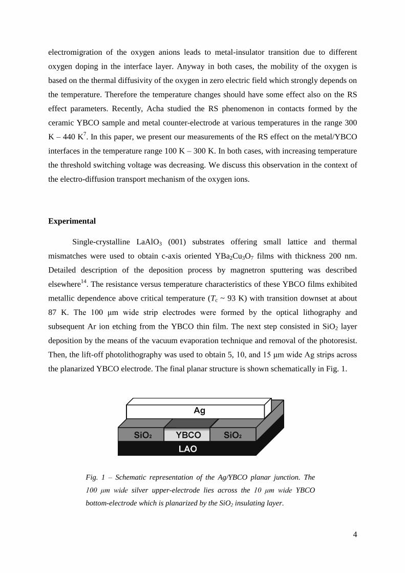
Single-crystalline LaAlO3 (001) substrates offering small lattice and thermal
mismatches were used to obtain c-axis oriented YBa2Cu3O7 films with thickness 200 nm.
Detailed description of the deposition process by magnetron sputtering was described
elsewhere14
. The resistance versus temperature characteristics of these YBCO films exhibited
metallic dependence above critical temperature (Tc ~ 93 K) with transition downset at about
87 K. The 100 μm wide strip electrodes were formed by the optical lithography and
subsequent Ar ion etching from the YBCO thin film. The next step consisted in SiO2 layer
deposition by the means of the vacuum evaporation technique and removal of the photoresist.
Then, the lift-off photolithography was used to obtain 5, 10, and 15 μm wide Ag strips across
the planarized YBCO electrode. The final planar structure is shown schematically in Fig. 1.
Fig. 1 – Schematic representation of the Ag/YBCO planar junction. The
100 μm wide silver upper-electrode lies across the 10 μm wide YBCO
bottom-electrode which is planarized by the SiO2 insulating layer.
5
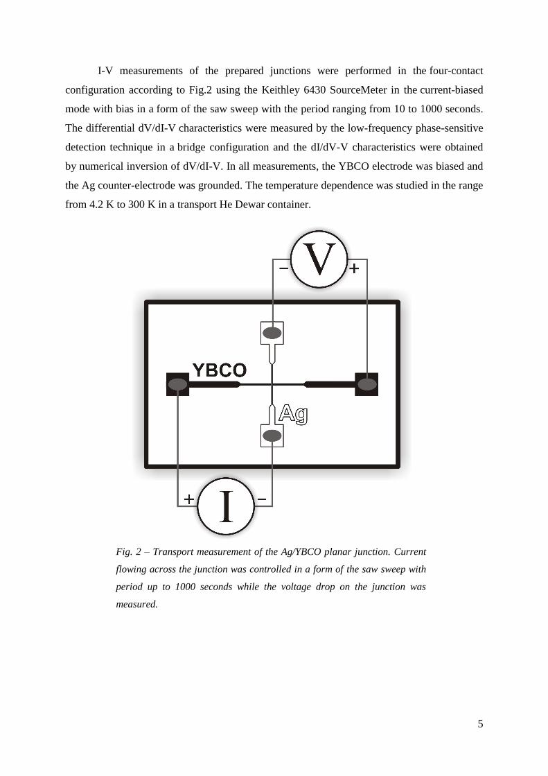
I-V measurements of the prepared junctions were performed in the four-contact
configuration according to Fig.2 using the Keithley 6430 SourceMeter in the current-biased
mode with bias in a form of the saw sweep with the period ranging from 10 to 1000 seconds.
The differential dV/dI-V characteristics were measured by the low-frequency phase-sensitive
detection technique in a bridge configuration and the dI/dV-V characteristics were obtained
by numerical inversion of dV/dI-V. In all measurements, the YBCO electrode was biased and
the Ag counter-electrode was grounded. The temperature dependence was studied in the range
from 4.2 K to 300 K in a transport He Dewar container.
Fig. 2 – Transport measurement of the Ag/YBCO planar junction. Current
flowing across the junction was controlled in a form of the saw sweep with
period up to 1000 seconds while the voltage drop on the junction was
measured.
6
Results and discussion
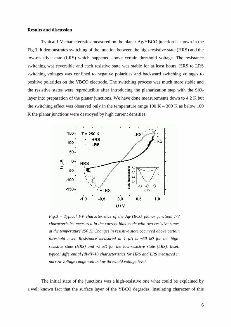
Typical I-V characteristics measured on the planar Ag/YBCO junction is shown in the
Fig.3. It demonstrates switching of the junction between the high-resistive state (HRS) and the
low-resistive state (LRS) which happened above certain threshold voltage. The resistance
switching was reversible and each resistive state was stable for at least hours. HRS to LRS
switching voltages was confined to negative polarities and backward switching voltages to
positive polarities on the YBCO electrode. The switching process was much more stable and
the resistive states were reproducible after introducing the planarization step with the SiO2
layer into preparation of the planar junctions. We have done measurements down to 4.2 K but
the switching effect was observed only in the temperature range 100 K – 300 K as below 100
K the planar junctions were destroyed by high current densities.
Fig.3 – Typical I-V characteristics of the Ag/YBCO planar junction. I-V
characteristics measured in the current bias mode with two resistive states
at the temperature 250 K. Changes in resistive state occurred above certain
threshold level. Resistance measured at 1 μA is ~50 kΩ for the high-
resistive state (HRS) and ~5 kΩ for the low-resistive state (LRS). Inset:
typical differential (dI/dV-V) characteristics for HRS and LRS measured in
narrow voltage range well below threshold voltage level.
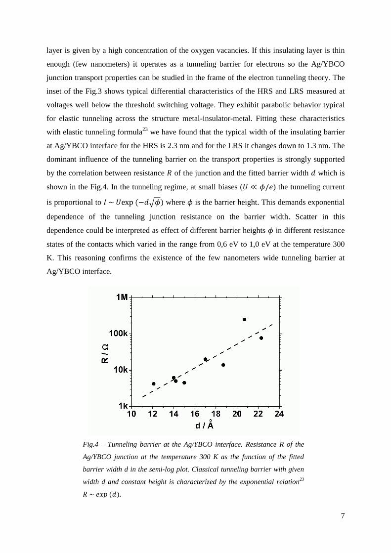
The initial state of the junctions was a high-resistive one what could be explained by
a well known fact that the surface layer of the YBCO degrades. Insulating character of this
7
layer is given by a high concentration of the oxygen vacancies. If this insulating layer is thin
enough (few nanometers) it operates as a tunneling barrier for electrons so the Ag/YBCO
junction transport properties can be studied in the frame of the electron tunneling theory. The
inset of the Fig.3 shows typical differential characteristics of the HRS and LRS measured at
voltages well below the threshold switching voltage. They exhibit parabolic behavior typical
for elastic tunneling across the structure metal-insulator-metal. Fitting these characteristics
with elastic tunneling formula23
we have found that the typical width of the insulating barrier
at Ag/YBCO interface for the HRS is 2.3 nm and for the LRS it changes down to 1.3 nm. The
dominant influence of the tunneling barrier on the transport properties is strongly supported
by the correlation between resistance of the junction and the fitted barrier width which is
shown in the Fig.4. In the tunneling regime, at small biases ( ) the tunneling current
is proportional to where is the barrier height. This demands exponential
dependence of the tunneling junction resistance on the barrier width. Scatter in this
dependence could be interpreted as effect of different barrier heights in different resistance
states of the contacts which varied in the range from 0,6 eV to 1,0 eV at the temperature 300
K. This reasoning confirms the existence of the few nanometers wide tunneling barrier at
Ag/YBCO interface.
Fig.4 – Tunneling barrier at the Ag/YBCO interface. Resistance R of the
Ag/YBCO junction at the temperature 300 K as the function of the fitted
barrier width d in the semi-log plot. Classical tunneling barrier with given
width d and constant height is characterized by the exponential relation23
.
8
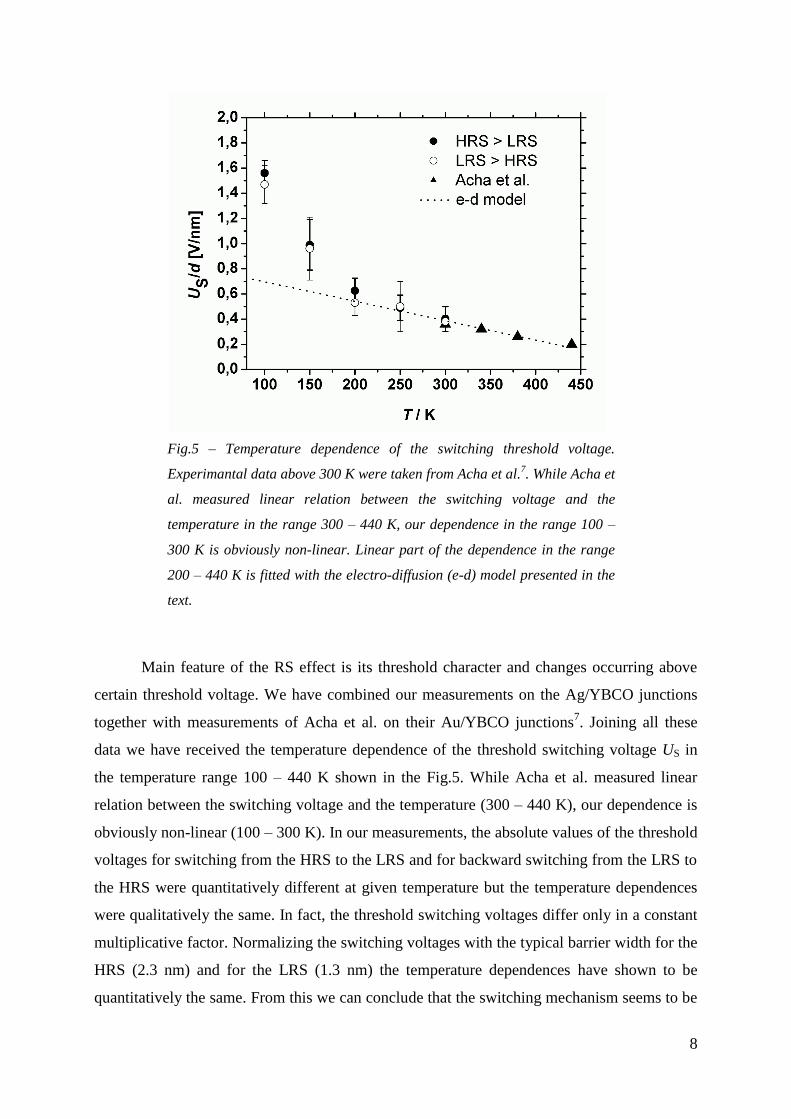
Fig.5 – Temperature dependence of the switching threshold voltage.
Experimantal data above 300 K were taken from Acha et al.7. While Acha et
al. measured linear relation between the switching voltage and the
temperature in the range 300 – 440 K, our dependence in the range 100 –
300 K is obviously non-linear. Linear part of the dependence in the range
200 – 440 K is fitted with the electro-diffusion (e-d) model presented in the
text.
Main feature of the RS effect is its threshold character and changes occurring above
certain threshold voltage. We have combined our measurements on the Ag/YBCO junctions
together with measurements of Acha et al. on their Au/YBCO junctions7. Joining all these
data we have received the temperature dependence of the threshold switching voltage US in
the temperature range 100 – 440 K shown in the Fig.5. While Acha et al. measured linear
relation between the switching voltage and the temperature (300 – 440 K), our dependence is
obviously non-linear (100 – 300 K). In our measurements, the absolute values of the threshold
voltages for switching from the HRS to the LRS and for backward switching from the LRS to
the HRS were quantitatively different at given temperature but the temperature dependences
were qualitatively the same. In fact, the threshold switching voltages differ only in a constant
multiplicative factor. Normalizing the switching voltages with the typical barrier width for the
HRS (2.3 nm) and for the LRS (1.3 nm) the temperature dependences have shown to be
quantitatively the same. From this we can conclude that the switching mechanism seems to be
9
similar at both polarities as it happens at constant electric field intensity for given temperature
(typically 5.106 V/cm). To match Acha’s temperature dependence to ours at common point
(300 K), it was necessary to normalize their data by a larger factor from what it follows that
their degraded layer was much thicker (d ~ 25 nm). In fact, the width of the degraded layer is
strongly depended on the maximum temperature involved in the process of thin films
creation. The degraded layer is thicker as the higher temperature is involved and it could be
up to hundreds of nanometers24
. In our case, before deposition of the upper metal electrode we
have performed the ion etching of the YBCO surface what lead to complete removal of the
degraded layer and its new creation at room temperature when oxygen diffusivity is much
lower then at typical temperatures during the YBCO thin film annealing process (500 °C). At
room temperatures the degraded layer of just a few nanometers appears25
.
We suppose that a key role in the RS effect plays the oxygen rearrangement just in the
degraded layer on the interface. It seems reasonable as the resistivity of the oxygen deficient
YBCO (ρ > 1000 mOhm.cm) is a few orders higher than that of the metallic phase (ρ < 1
mOhm.cm) located behind the degraded layer. Hence almost all voltage bias between metal
electrodes drops on the interface and the electric field is concentrated in the thin degraded
layer and can reach intensities up to 107 V/cm. In this case, the mobility of the oxygen ions is
significantly enhanced by the electrical field and highly overcomes the basal diffusive
mobility due to thermal excitations. In this case the movement of the oxygen ions must be
studied in the electro-diffusion model. We describe the basal oxygen motion in absence of the
electric field in the frame of the barrier diffusion model which is based on one dimensional
system of narrow energetic barriers with height (activation energy for oxygen motion)
with separation . Then the rate of oxygen jumps over activation barriers between two
adjacent oxygen sites 1 and 2 is given as15
:
(1)
where is the attempt frequency. Applying the voltage on such system we expect that the
electric field with the magnitude is concentrated on the insulating layer with
thickness . Electric field causes acceleration of double charged oxygen ions on the distance
between the oxygen sites, gain of the energy for the O2–
ion what leads to enhanced
probability for occurrence of the overcomes in the direction of the electric force comparing
with opposite one:
10
(2)
As a result an average drift velocity arises in the direction of the electric force:
(3)
Last approximation is valid when what is completely fulfilled at studied
intensities up to 107 V/cm. At low voltage biases the mobility of ions is several orders of
magnitude lower then effective mobility of charge carriers passing the interface. Therefore,
under the threshold switching voltage when current density is typically below 10 ÷ 100
mA.mm-2
(in ours as in Acha’s experiments) we measure only the electronic conductivity.
When the drift velocity of oxygen ions exceeds a critical value ( ), instabilities in the ion
system can take place similar to electrical instabilities in semiconductors. The observations
are very similar to the known electrical instabilities in semiconductors driven far from
thermodynamic equilibrium by strong external fields causing switching between high-
resistive and low-resistive states26
. If existence of a critical drift velocity is supposed to be
a threshold for occurrence of the switching phenomenon then we can derive the threshold
voltage defined as:
(4)
Then, the threshold voltage at the zero temperature simply means the voltage level at which
the kinetic energy of the ion gained in the electrical field equals the activation energy for
movement from one unit cell to another. In that case, Eq. (4) simplifies to .
Rising the absolute temperature, effective activation energy is reduced by the factor
and the threshold voltage is decreasing correspondingly. Such model gives linear
relation between the switching voltage and the absolute temperature with the main
parameters: the oxygen mean free path and the activation energy . Parameters ,
occurs under logarithm therefore they are of second order of importance and their
approximation in orders of magnitude is sufficient according to roughness of the model.
Attempt frequency is typically in order of 1012
Hz27
. Using the approximation for the
mobile oxygen content in the barrier layer with the assumption of the one mobile oxygen per
11
unit cell ( ) we have estimated the critical drift velocity for
entire temperature range from measured critical current densities and relation .
Fitting the linear part of the temperature dependence over 200 K (Fig.5), we have
received the model parameters: and . Obtained value of the activation
energy for the oxygen motion is in good agreement with previous works15,24,28-30
. It is
interesting to take note of the deviation from the linear law below 200 K. According to
previous research this is a typical temperature below which the pseudo-gap and associated
effects based on the YBCO antiferromagnetic nature can be observed 11,18,31
. In this state the
spin correlation interactions are much stronger causing additional oxygen ordering in the CuO
chains. The transition into a more ordered state increases the activation energy for the oxygen
motion and reduces the oxygen diffusion. Therefore, also the electromigration based on the
oxygen ions diffusivity is strongly suppressed what demands stronger electrical field for
occurrence of the RS effect.
Conclusion
RS effect observed on metal/YBCO junctions in the temperature range 100-440 K was
discussed within the electro-diffusion model, taking into account oxygen ions drift in the
nanometer scale vicinity of the junction interface under applied electrical fields. The model
leads to linear relation between switching voltage and the temperature while the measured
dependence deviates from the linear law under 200 K. This point is worth of further
investigation as the similar effect was observed also on our PtIr/YBCO contacts14
. It seems
that the interconnection between effects of the strongly correlated systems and the role of the
oxygen electromigration is more striking below this temperature.
References
1M. Hamaguchi, K. Aoyama, S. Asanuma, Y. Uesu, and T. Katsufuji, Appl. Phys. Lett. 88,
142508 (2006).
2R. Waser, and M. Aono, Nature Mater. 6, 833 (2007).
3A. Sawa, Mater. Today 11, 28 (2008).
12
4T.W. Hickmott, J. Appl. Phys. 33, 2669 (1962).
5J.F. Gibbons, and W.E. Beadle, Solid-State Electron. 7, 785 (1964).
6B. J. Choi, D. S. Jeong, S. K. Kim, C. Rohde, S. Choi, J. H. Oh, H. J. Kim and C. S. Hwang,
J. Appl. Phys. 98, 033715 (2005).
7C. Acha, Physica B 404, 2746 (2009).
8N. A. Tulina, I. Yu. Borisenko, V. V. Sirotkin, Phys. Lett. A 372, 6681 (2008).
9M. Belogolovskii, Centr. Eur. J. Phys. 7(2), 304-309 (2009)
10A. Plecenik, M. Grajcar, P. Seidel, and S. Benacka, Studies of High Temperature
Superconductors, edited by A. Narlikar (Nova Science Publisher, New York, 1996), Vol. 20,
p.75.
11P. A. Lee, N. Nagaosa, and X. Wen, Rev. Mod. Phys. 78, 17 (2006).
12A. Sawa, T. Fujii, M. Kawasaki, and Y. Tokura, Appl. Phys. Lett. 85, 4073 (2004).
13T. Fujii, M. Kawasaki, A. Sawa, and Y. Kawazoe, Phys. Rev. B 75, 165101 (2005).
14A. Plecenik., et al., Appl. Surf. Sci. 256, 5684 (2010).
15M. Grajcar, A. Plecenik, M. Darula, and S. Benacka, Solid. Stat. Comm. 81, 191 (1992).
16K. N. Tu, N. C. Yeh, S. I. Park, and C. C. Tsuei, Phys. Rev. B 39, 304 (1989).
17L. F. Rybalchenko, and Y. K. Yanson, Physica C 224, 38 (1994).
18A. Plecenik, M. Grajcar, P. Seidel, P. Takacs, A. Matthess, M. Zuzcak, and S. Benacka,
Physica C 301, 234 (1998).
19N.F. Mott, et al., Phil. Mag. 6, 287 (1961).
20R. Fors, S. I. Khartsev, and A. M. Grishin, Phys. Rev. B 71, 045305 (2005).
21D. C. Kim, et al., Appl. Phys. Lett. 88, 202102 (2006).
22M. J. Rozenberg, I. H. Inoue, and M. J. Sanchez, Appl. Phys. Lett. 88, 033510 (2006).
13
23E. L. Wolf, Principles of Electron Tunneling Spectroscopy (Oxford University Press, New
York, 1989) p.37.
24S. J. Rothman, J. L. Routbort, and J. E. Baker, Phys. Rev. B 40, 8852 (1989).
25R. Mogilevsky, et. al., Phys. Rev. B 49, 6420 (1994)
26E. Schöll, Advances in Solid State Physics 26, 309 (1986)
27A.-K. Klehe, et. al., Physica C 257, 105 (1996).
28X. Zhang, and C. R. A. Catlow, Phys. Rev. B 46, 457 (1992).
29M. Runde, J. L. Routbort, and S. J. Rothman, Phys. Rev. B 45, 7375 (1992).
30A. Michaelis, E. A. Irene, O. Auciello, and A. R. Krauss, J. Appl. Phys. 83, 7736 (1998).
31A. Plecenik, M. Grajcar, P. Seidel, and S. Benacka, Studies of High Temperature
Superconductors, edited by A. Narlikar (Nova Science Publisher, New York, 1996), Vol. 20,
p.84.


![Radiation Hardening by Process of CBRAM Resistance ......2020/01/06 · CBRAM, a cation based resistance switching technology [4], [8]. Additionally, recent results have demonstrated](https://static.fdocuments.net/doc/165x107/5ff833516ab95630e4480c2f/radiation-hardening-by-process-of-cbram-resistance-20200106-cbram.jpg)


