Technology Roadmap for 22nm CMOS and beyond · 22nm CMOS and beyond June 1, 2009 Hiroshi Iwai Tokyo...
59
1 Technology Roadmap for 22nm CMOS and beyond June 1, 2009 Hiroshi Iwai Tokyo Institute of Technology IEDST 2009@IIT-Bombay
Transcript of Technology Roadmap for 22nm CMOS and beyond · 22nm CMOS and beyond June 1, 2009 Hiroshi Iwai Tokyo...

1
Technology Roadmap for 22nm CMOS and beyond
June 1, 2009
Hiroshi Iwai
Tokyo Institute of Technology
IEDST 2009@IIT-Bombay

22
Outline
1. Scaling
4. SRAM Cell Scaling
2. ITRS Roadmap
3. Voltage Scaling/ Low Power and Leakage
5.Roadmap for further futureas a personal view

33
1. Scaling

44
Scaling Method: by R. Dennard in 1974
1
1Wdep
1 1
I
00 V 1
X , Y , Z : K, V : K, Na : 1/K
K
K
KWdep
Wdep V/Na: K
KI00 KV
I : K
K=0.7 for example
Wdep: Space Charge Region (or Depletion Region) Width
Wdep has to be suppressedOtherwise, large leakagebetween S and D
Leakage current
S D
By the scaling, Wdep is suppressed in proportion,and thus, leakage can be suppressed.
Good scaled I-V characteristics
Potential in space charge region ishigh, and thus, electrons in source areattracted to the space charge region.

55
Drive current
Power per chip
Integration (# of Tr)
Scaling K : K=0.7 for example
Id = vsatWgCo (Vg‐Vth)
N
K‐1(αK‐2)K (K1 )2= α
Switching speed KK/K= K
Id per unit Wg = Id / Wg= 1
Wg (tox –1)(Vg‐Vth)= Wgtox
‐1(Vg‐Vth)= KK‐1K=Kin saturation
Co: gate C per unit area
Cg = εoεoxLgWg/tox
Id per unit Wg
Clock frequency
K
1
τ
Id
K
Id/µm
f 1/K f = 1/τ = 1/K
N α/K2
P α
Gate capacitance Cg K
Chip area Achip α
Lg, WgTox, Vdd
Geometry &Supply voltage
K
KK/K = K
τ= CgVdd/Id
α: Scaling factor
α/K2
fNCV2/2
= 1/K2 , when α=1
= 1, when α=1
Downscaling merit: Beautiful!
In the past, α>1 for most cases

66
k= 0.72 =0.5 and α =1
Vdd 0.7Single MOFET
Lg 0.7Id 0.7Cg 0.7P (Power)/Clock
0.73 = 0.34 τ (Switching time) 0.7
Chip N (# of Tr) 1/0.72 = 2
P (Power)
k= 0.7 and α =1
Vdd 0.5Lg 0.5Id 0.5Cg 0.5P (Power)/Clock
0.53 = 0.125 τ (Switching time) 0.5
1/0.7 = 1.4f (Clock)1
N (# of Tr) 1/0.52 = 4
P (Power)1/0.5 = 2f (Clock)1

- However, down-scaling of CMOS is still the‘royal road’* for high performance and low power.
- The concerns for limits of down-scaling havebeen announced for every generation.
- Effort for the down-scaling has to be continuedby all means.
*Euclid of Alexandria (325BC?-265BC?)
Mencius (Meng-zi), China (372BC?-289BC?)
‘There is no royal road to Geometry’
(Rule of right vs. Rule of military)7

88
10 -3
10 -2
10 -1
10 0
10 1
10 2
1970 1980 1990 2000
MPU Lg (µm)X
j (µm)
Minimum logic Vdd (V)
Id/µm(mA/µm)
tox (µm)
10 -3
10 -1
10 1
10 3
1970 1980 1990 2000
chip size (mm2)
Number of tr
ansistors
power (W
)
MIPSclock frequency (MHz)
Id/µm
Id
1 101
10‐1K (10 –2) f 1/K(10 2) 103
P α(10 1) 105
N α/K2(10 5) 104Achip α 101
Change in 30 years
Lg K 10 ‐2tox K(10 –2) 10‐2
Vdd K(10 –2) 10‐1
Idealscaling
RealChange
Idealscaling
RealChange
Idealscaling
RealChange
= fαNCV2
Past 30 years scaling
N, f increaseMerit:
Demerit: P increase
Vdd scaling insufficient
Additional significantincrease inId, f, P
Actual past downscaling trend until year 2000
Vd scaling insufficient, α increased N, Id, f, P increased significantly
Source. Iwai and S. Ohmi, Microelectronics Reliability 42 (2002), pp.1251-1268

99
- Supply voltage reduction is becoming difficult,because Vth cannot be decreased any more,as described later.
- Now, power and/or heat generation are thelimiting factors of the down-scaling
- Growth rate in clock frequency and chip areabecomes smaller.

1010
2. ITRS Roadmap(for 22 nm CMOS logic)

11
What is a roadmap? What is ITRS?
ITRS: International Technology Roadmap for Semiconductorsmade by SIA (Semiconductor Industry Association with Collaboration with Japan, Europe, Korea and Taiwan)
0.1
1
10
100
1995 2005 2015
EOT
[nm
]
1
10
100
1000
1995 2005 2015
Phys
ical
Gat
e Le
ngth
[nm
]
19921994
19971999
2001
2003
2005
19921994
19971999
2001
2003
2005
40nm
1.5nm
ゲート長 ゲート絶縁膜厚
0.1
1
10
100
1995 2005 2015
EOT
[nm
]
1
10
100
1000
1995 2005 2015
Phys
ical
Gat
e Le
ngth
[nm
]
19921994
19971999
2001
2003
2005
19921994
19971999
2001
2003
2005
40nm
1.5nm
ゲート長 ゲート絶縁膜厚Gate length
Gate oxidethickness
Roadmap: Prediction of future technologies

2006 ITRSupdate
2007 ITRS
2008 ITRSupdate
1992 -1997:NTRS (National Technology Roadmap)1998 - : ITRS (International Technology Roadmap)

1313
ITRS Roadmap does change every year!
http://www.itrs.net/reports.html
2007 Edition2006 Update 2005 Edition2004 Update
2003 Edition2002 Update2001 Edition2000 Update

14
Subthreshold Leakage (A/µm)
Ope
ratio
n Fr
eque
ncy
(a.u
.)
e)100
10
1
Source: 2007 ITRS Winter Public Conf.
HP, LOP, LSTP for Logic CMOS

1515
45 nm
Starting Year2007
Technology name
Half Pitch(1st Metal)
PhysicalGate Length
for High Performance Logic
32 nm29 nm
68 nm59 nm
What does ‘45 nm’ mean in 45 nm CMOS Logic?
32 nm 2009? 27 nm24 nm
52 nm45 nm
‘XX nm’ CMOS Logic Technology:- In general, there is no common corresponding parameter with ‘XX nm’ in ITRS table, which stands for ‘XX nm’ CMOS.
ITRS (Likely in 2008 Update)
Year
200720082009 2010
‘XX nm CMOS TechnologyCommercial Logic CMOS products

1616
What does ‘45 nm’ mean in 45 nm CMOS Logic?8µm 6µm 4µm 3µm 2µm 1.2µm 0.8µm 0.5µm- Originally, ‘XX’ means lithography resolution.
- ‘XX’ had shrunk 0.7 in 3 years in average (0.5 in 6 years) those days.- Thus, ‘XX’ was the gate length, and half pitch of lines
Logic 1st Metal Half Pitch

1717
What does ‘45 nm’ mean in 45 nm CMOS Logic?
350nm 250nm 180nm 130nm 90nm 65nm 45nm-‘XX’ values were established by NTRS* and ITRS with the term of ‘Technology Node**’ and ‘Cycle***’ using typical ‘half pitch value’.
- The gate length of logic CMOS became smaller with one ortwo generations from the half pitch, and ‘XX’ names aheadof generations have been used for logic CMOS.
- Memory still keeps the half pitch as the value of ‘XX’
Resist
ResistAshing

1818
For example, Typical Half Pitches at ITRS 2007
Resist
ResistAshing
Source: 2008 ITRS Summer Public Conf.

1919
Physical gate length in past ITRS was too aggressive.The dissociation from commercial product prediction will be adjusted.
Physical gate length of High-Performance logic will shift by 3-5 yrs.
45nm 32nm 22nm Logic CMOS
2008 Update Phys. LgITRS 2007 Phys. Lg
2008 Update Print Lg
X0.71 / 3 YearITRS 2007 Print Lg
X0.71 / 3.8 Year
X0.71 / 3 Year
X0.71 / 3 Year
32nm 27nm 22nm25nm 20nm 16nm
3 year shift
Correspond to
Source: 2008 ITRS Summer Public Conf.

2020
EOT and Xj shift backward, corresponding to Lg shift
filled in for metal gate EOT for 2009/10 based on latest conference presentations
non-steady trendcorrected
Likely in 2008 Update
Likely in 2008 Update
Likely in 2008 Update
Likely in 2008 Update
Correspond to 22nm
8
EOT: 0.55 nm 0.88 nm, Xj: 8 nm 11 nm @ 22nm CMOS
Source: 2008/ ITRS Summer Public Conf.

2121
22 nm
45 nm
Starting Year
2011?~2012?
2007
Technology name
Half Pitch(1st Metal)
PhysicalGate Length
for High Performance Logic
22 nm20 nm
32 nm29 nm
16 nm 2013?~2014?
18 nm16 nm
68 nm59 nm
40 nm36 nm32 nm29 nm
What does ‘22 nm’ mean in 22 nm CMOS Logic?
Source: 2008 ITRS Summer Public Conf.
32 nm 2009? 27 nm24 nm
52 nm45 nm
From ITRS2008 Update, maybe XX nm stands for the physicalGate length
ITRS (Likely in 2008 Update)
Year
20112012
20072008
20132014
2009 2010
‘XX nm CMOS TechnologyCommercial Logic CMOS products

2222
Advantage in RISCSimple configuration
Advantage in SISCEra for ‘out of order’
Multi CoreClock ≠
Performance
Source: Mitsuo Saito, Toshiba
Clock frequency does not increase aggressively anymore.Even decreased!

23Source: 2007 ITRS Winter Public Conf.
ITRS2007
Core Clock
Frequency
ChipFrequency
Continued?
Cell Broadband Engine
Source:IBM, Toshiba, SonyISSCC2008 and 08
6GHz capability for SRAM

2424
ITRS2001
ITRS2003
ITRS2005
ITRS2007
Clock frequency Change in the past ITRS (Max on chip frequency or ‘Core clock’)
15%/Year
8%/Year
22 nm: 6 GHz?
Source: 2008 ITRS Summer Public Conf.
2525
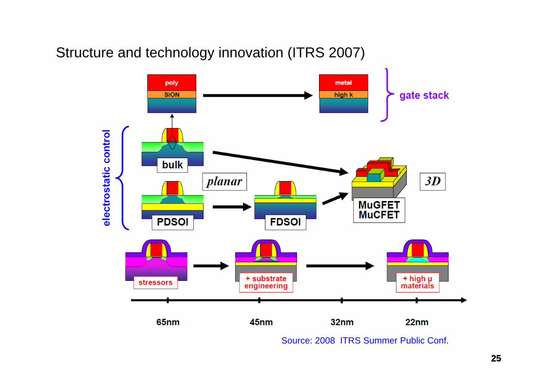
Structure and technology innovation (ITRS 2007)
Source: 2008 ITRS Summer Public Conf.

2626
Timing of CMOS innovations shifts backward.
Correspond to 22nm Logic CMOS
Bulk extends 4 years!
Multi G delays 4 years!
Source: 2008 ITRS Summer Public Conf.
Bulk CMOS has longer life now!

2727
Source: ITRS 2007
Wafer size (ITRS 2007)Correspond to 22nm
??Maybe delay??

2828
ITRS2008 Low-k Roadmap Update
ITRS2007
Update2008ITRS2007
Update2007
k value increases by 0.1 ~ 0.3
Correspond to 22nm Logic
Source: 2008 ITRS Summer Public Conf.

2929
ITRS1999
Historical Transition of ITRS Low-k Roadmap
ITRS2001
ITRS2003
ITRS2005ITRS2007,8
Source: 2008 ITRS Summer Public Conf.

3030
Roadmap towards 22nm technology and beyond
- Physical gate length downsizing rate will be less aggressive.
- Corresponding to the above, performance increase would slow down – Clock frequency, etc.
- Introduction of innovative structures – UTB SOI andDG delayed, and bulk CMOS has longer life thanpredicted by previous ITRS roadmaps.

3131
3. Voltage Scaling/ Low Power and Leakage

3232
Difficulty in Down-scaling of Supply Voltage: Vdd
Year
Vdd
VthVol
t
Subthreshold leakage current limit> ∆VthMargin for Vth variationis necessary
Vdd – Vth determines theperformance (High Id)and cannot be too small.
∆Vth: Vth variation
Because, Vth cannotbe down-scaled anymore,Vdd down-scaling is difficult.

3333
Vg
Id
Vth (Threshold Voltage)
Vg=0V
SubthreshouldLeakage Current
Subtheshold leakage current of MOSFET
Subthreshold CurrentIs OK at Single Tr. level
But not OKFor Billions of Trs.
ONOFF
Ion
Ioff
Subthresholdregion

3434
Vg (V)
10-7A
Vg = 0V
Vth = 300mVVth= 100mV
Vth down-scaling
Subthreshold slope (SS)= (Ln10)(kT/q)(Cox+CD+Cit)/Cox> ~ 60 mV/decade at RT
SS value: Constant and does not become small with down-scaling
10-3A
10-4A
10-5A
Vdd=0.5V Vdd=1.5V
Ion
Ioff
Ioff
10-6A
10-8A
10-9A
10-10ALog
Id p
er u
nit g
ate
wid
th (=
1µm
)
Vdd down-scaling
Log scale Id plot
Ioff increaseswith 3.3 decades(300 – 100)mV/(60mv/dec)= 3.3 dec
Vth cannot be decreased anymore
Vth: 300mV 100mV
significant Ioff increase

35
Year
Ion/
Ioff
ratio
1.0E+3
1.0E+4
1.0E+5
1.0E+6
1.0E+7
1.0E+8
1.0E+9
2004 2007 2010 2013 2016 2019 2022
2008up (bulk)2008up (UTB)2008up (DG)2007 (bulk)2007 (UTB)2007 (DG)2005 (bulk)2005 (UTB)2005 (DG)200320011999
Ion/Ioff ratio
2001
1999
2005 DGOthers
2003-2008
35
Source: ITRS and2008 ITRS Summer Public Conf.
ITRS for HP logic
2008 Values are from ITRS Public Conf. and still under discussion

36Year
Vd
d (
V)
0
0.2
0.4
0.6
0.8
1
1.2
2004 2007 2010 2013 2016 2019 2022
2008up (bulk)2008up (UTB)2008up (DG)2007 (bulk)2007 (UTB)2007 (DG)2005 (bulk)2005 (UTB)2005 (DG)200320011999 0
0.05
0.1
0.15
0.2
0.25
0.3
0.35
0.4
2004 2007 2010 2013 2016 2019 2022
2008up (bulk)2008up (UTB)2008up (DG)2007 (bulk)2007 (UTB)2007 (DG)2005 (bulk)2005 (UTB)2005 (DG)2003 (bulk)
Year
Vth
(V
)
36
Vdd Saturated Vth
2008
2005 Blk
2003, 2005, 2007
1999
2001
2007, 2008
2003
2005 UTB
2005 DG
Source: ITRS and2008 ITRS Summer Public Conf.
ITRS for HP logic
2008 Values are from ITRS Public Conf. and still under discussion
Vdd will stay higherin 2008 update
Vth-sat will bearound 0.1V

3737
Vth-sat / Vdd
Source: ITRS and2008 ITRS Summer Public Conf.
ITRS for HP logic
0
0.05
0.1
0.15
0.2
0.25
0.3
0.35
0.4
2004 2007 2010 2013 2016 2019 2022
2008up (bulk)2008up (UTB)2008up (DG)2007 (bulk)2007 (UTB)2007 (DG)2005 (bulk)2005 (UTB)2005 (DG)2003 (bulk)
Year
Vth/
Vdd 2007
2008
2003
2005
2008 Values are from ITRS Public Conf. and still under discussion

3838
Could we squeeze technologies for ultimate CMOS scaling?Saturation of EOT thinning is a serious roadblock to proper down-scaling.
0.4
0.6
0.8
1
1.2
2004 2007 2010 2013 2016 2019 2022
2008up (bulk)2008up (UTB)2008up (DG)2007 (bulk)2007 (UTB)2007 (DG)2005 (bulk)2005 (UTB)2005 (DG)2003 (bulk)20011999
Year
EOT
(nm
)
Is 0.5nm real limit?
for H
P Lo
gic
DelaySaturation
Gate Oxd C
Inversion C
Interfacial C@Metal gate andGate oxd.(EOT=0.2~0.3nm?)
(EOT=0.3~0.5nm?)
Metal gateHigh-k oxd
Si
Interfacial C(Quantum eff)
Inversion C(Quantum eff)
EOT(C1) + EOT(C3) > 0.5nm
C1
C2
C3
Small effect to decreaseEOT(C2) beyond 0.5nm?
Improper down-scaling
3939
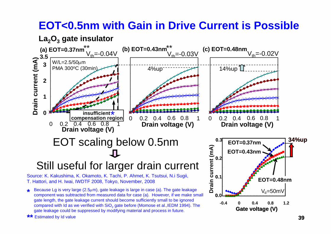
EOT<0.5nm with Gain in Drive Current is Possible
Source: K. Kakushima, K. Okamoto, K. Tachi, P. Ahmet, K. Tsutsui, N.i Sugii, T. Hattori, and H. Iwai, IWDTF 2008, Tokyo, November, 2008
EOT scaling below 0.5nm
Still useful for larger drain current
0 0.2 0.4 0.6 0.8 1 0 0.2 0.4 0.6 0.8 1 0 0.2 0.4 0.6 0.8 1
Dra
in c
urre
nt (m
A) 3.5
2
1
0
3
(a) EOT=0.37nm (b) EOT=0.43nm (c) EOT=0.48nm
W/L=2.5/50µmPMA 300oC (30min)
Vth=-0.04V Vth=-0.03V Vth=-0.02V
14%up4%up
0 0.2 0.4 0.6 0.8 1Drain voltage (V)
0 0.2 0.4 0.6 0.8 1Drain voltage (V)
0 0.2 0.4 0.6 0.8 1Drain voltage (V)
compensation regioninsufficient*
* Because Lg is very large (2.5µm), gate leakage is large in case (a). The gate leakage component was subtracted from measured data for case (a). However, if we make small gate length, the gate leakage current should become sufficiently small to be ignored compared with Id as we verified with SiO2 gate before (Momose et al.,IEDM 1994). The gate leakage could be suppressed by modifying material and process in future.
-0.4 0 0.4 0.8 1.2Gate voltage (V)
0.3
Dra
in c
urre
nt (m
A)
0.2
0.1
0.0
EOT=0.37nmEOT=0.43nm
Vd=50mV
34%up
EOT=0.48nm
-0.4 0 0.4 0.8 1.2Gate voltage (V)
0.3
0.2
0.1
0.0
EOT=0.37nmEOT=0.43nm
Vd=50mV
34%up
EOT=0.48nm
La2O3 gate insulator** **
** Estimated by Id value

40
Thus, in future, maybe continuous development of new techniques could make more proper down-scaling possible.
It is difficult to say, but EOT and Vdd may become smaller than expected today.

41Source: 2007 ITRS Winter Public Conf.
Nor
mal
ized
σVt
hRandom Variability Reduction Scenarioin ITRS 2007

4242
4. SRAM cell scaling

4343
90 nm Process1.0 µm2cell50 Mbit109 mm2
February ‘02
32 nm Process0.182 µm2cell291 Mbit118 mm2
September ‘07
65 nm Process0.57 µm2cell70 Mbit110 mm2
April ‘04
45 nm Process0.346 µm2cell153 Mbit119 mm2
January ‘06
0.5 X every 2 years
1995 2000 2005 20100.1
1
10
Cel
l are
a (µ
m2 )
Year
32nm
45nm65nm
90nm
130nm
180nm 0.5 X every 2 years
1995 2000 2005 20100.1
1
10
Cel
l are
a (µ
m2 )
Year1995 2000 2005 20100.1
1
10
1995 2000 2005 20101995 2000 2005 20100.1
1
10
0.1
1
10
Cel
l are
a (µ
m2 )
Year
32nm
45nm65nm
90nm
130nm
180nm
Intel’s SRAM test chip trend
Processname
Lithography 1st production
P1264
P1266
P1268
P1270
65nm
45nm
32nm
22nm
2005
2007
2009
2011
Source: B. Krzanich, S. Natrajan, Intel Developer’s Forum 2007http://download.intel.com/pressroom/kits/events/idffall_2007/BriefingSilicon&TechManufacturing.pdf
SRAM down-scaling trendhas been kept until 32nmand probably so to 22nm
Only schedule has been published
Chip areaFunctional Si
CapacityCell sizeTechnology

4444Source: IEDM2008 Pre-conference Publicity
http://www.btbmarketing.com/iedm/
Announced on Aug 18, 2008
Source: http://www-03.ibm.com/press/us/en/pressrelease/24942.wss
22 nm technology 6T SRAM Cell: Size = 0.1µm
Consortium: IBM (NYSE) , AMD, Freescale, STMicroelectronics, Toshiba and the College of Nanoscale Science and Engineering (CNSE)
- High-NA immersion lithography- High-K metal gate stacks- 25 nm gate lengths- Thin composite oxide-nitride spacers- Advanced activation techniques- Extremely thin silicide- Damascene copper contacts
New technologies introduced
0.1µm cell size is almost on the down-scaling trend
Static noise marginof 220 mV at 0.9 V

4545
Cel
l are
a (µ
m2 ) 0.57µm2
0.35µm2
0.18µm2
0.15µm2
0.24µm2
0.1µm2
65nm 45nm 32nm 22nm
1
0.1
1/2 per cycle
2/3 per cycle
0.2
0.5 Intel
IBM Alliance
TSMC
Intel
65nm Apr.200445nm Jan.200632nm Sep.2007
TSMC
45nm Dec.200732nm Dec.2007
IBM Alliance(Consortium)
32nm Dec.2007
22nm Aug.2008
Cell size reduction trends
1/2 or 2/3 per cycle? Functional Si
Conference (IEDM)
Conference (IEDM)
Press release

4646
Source: K.J.KuhnIEDM 2007
Nor
mal
ized
to
180
nm
NMOS Mismatch Coefficient (C2) improvement with technology scaling
C2

4747
Source: K. J. Kuhn IEDM2007 Tech. Dig. pp.471
Mismatch improvement by layout (Intel)
45nm 0.346 µm2
65nm : 0.57 µm2
90nm :1.0 µm2
“tall” design
“wide”design
“wide” design (Square endcaps)

Double patterning for square endcap
Source: M. Bohr, ICSICT2008
48
TSMC 45nmTSMC 32nm
IBM Alliance 32nm
IEDM 2007
IEDM 2007
IEDM 2004IEDM 2008
TSMC 45nm TSMC 32nm IBM Gr. 32nm
Cell evolution is similar
IBM Alliance 22nm

4949
Most Difficult part of SRAM down-scaling is Vdd down-scaling
Density of on-chip cache SRAM memory is highand thus, Vth cannot be down-scaled too much because of large Isd-leak
Also, under low Vdd, read- and write margin degrades, data retention degrade.
Thus, Vdd down-scaling is more severe in SRAMthan logic part of the circuits

5050
Intel® Xeon® 7400 Series (Dunnington)
45 nm high-k6 cores
Source: Intel Developer Forum 2008
Cache occupies huge area
16MB shared L3 cache
Cell size of SRAM should be minimized
Isd-leak should be minimized
Vth are often designed to be higher than Min. logic Vth
Lg are often designed to be larger than Min. logic Lg

Voltage/Frequency Partitioning
DDR VccCore VccUncore Vcc
Nehalem(Intel) 2,4 or 8 Cores
Dynamic Power Management
32kB L1 I -cache32kB L1 D-cache256kB L2 -cache
8 MB L3 cache
Chip
Core
8T SRAMCell
6T SRAMCell
51Source: Intel Developer Forum 2008

Source: Morita et. al, Symp. on VLSI Circ. 2007
6T and 8T Cell
6T Cell
8T Cell
Cell size is smallFor high density use
Cell size increase 30%
Add separate read function
For low voltage use
52

5353
5. Roadmap for further futureas a Personal View

5454Source: 2008 ITRS Summer Public Conf.
ITRS figure edited by Iwai
5.5nm? was added by Iwai*
5.5nm?*
3 important innovations
-There will be still 4~6 cycles (or technology generations) left untilwe reach 11 ~ 5.5 nm technologies, at which we will reach down-scaling limit, in some year between 2020-30 (H. Iwai, IWJT2008).
-Even After reaching the down-scaling limit, we could still continueR & D, seeking sufficiently higher Id-sat under low Vdd.
-Two candidates have emerged for R & D
2. Alternative channel MOSFETs (III-V, Ge)1. Nanowire/tube MOSFETs
- Other Beyond CMOS devices are still in the cloud.

55
Si nanowire FET with Semi-1D Ballistic TransportReduction in Ioff (Isd-leak)0
Good control of Isd-leak by surrounding gate
Increase in Ion (Id-sat)
High Conduction (1D)Go=77.8µS/wire
Multiple quantum channel (QC) used for conduction
High-density lateraland vertical integration
Merit of Si-nanowire
Trade off
Source: Y. Lee., T. Nagata., K. Kakushima., K. Shiraishi, and H. Iwai, IWDTF 2008, Tokyo, November, 2008
Source: T. Ohno, K. Shiraishi, and T. Ogawa, Phys. Rev. Lett. ,1992
Carrier scattering probabilitySmall Large
# of quantum channelSmall Large

Our roadmap for R &D Source: H. Iwai, IWJT 2008
Current Issues
III-V & Ge NanowireHigh-k gate insulatorWire formation technique
CNT:
Width and Chirality control Growth and integration of CNT
Graphene:Graphene formation technique Suppression of off-current
Very small bandgap or no bandgap (semi-metal)
Control of ribbon edge structure which affects bandgap
Chirality determines conduction types: metal or semiconductor
56
Si NanowireControl of wire surface property
Compact I-V model
Source Drain contactOptimization of wire diameter

57
Source: H. Iwai, IPFA 2006Size(Gate length etc)
Saturation of Downsizing
Some time in 2020 - 2030
5 n
m?
New Materials, New Process, New Structure(Logic, Memory)
Hybrid integration of different functional Chip Increase of SOC functionality
3D integration of memory cell3D integration of logic devices
Low cost for LSI processRevolution for CR,Equipment, Wafer
Miniaturization of Interconnectson PCB(Printed Circuit Board)
Introduction of algorithmof bio-systemBrain of insects, human
After 2050?
We do not know how?
Long term roadmap for development We do know system and algorithms are important!
But do not know how it can be by us for use of bio?

58
Acknowledgement
Kuniyuki Kaukshima, Parhat Ahmet, Takamasa Kawanago, Yeonghun Lee
ITRS Committee: Hidemi Ishiuchi (Toshiba), Paolo Gargini (Intel)
Toshiba Corporation: Mitsuo Saito, Yukihiro Urakawa, Tomoaki Yabe
Tsukuba University: Kenji Shiraishi, Kenji Natori
Intel Corporation: Mark Bohr
I would like to express deep appreciation to the following people for the useful advice and support for material preparation.Special thanks to ITRS committee for the permission to refer roadmap and Public conference.
Tokyo Institute of Technology:
IBM Alliance : B.S. Haran et al,

59
Thank you for your attention!