Technologies for High Performance Portable Healthcare Devices · 2015-03-06 · Technologies for...
16
Technologies for High Performance Portable Healthcare Devices www.analog.com/healthcare Contents MEMS Inertial Sensors.............................................. 3 MEMS Microphones .................................................. 4 Photocurrent-to-Voltage Amplifiers ........................... 5 Impedance Converter System .................................. 6 Capacitive-to-Digital Controllers................................ 7 Low Power, High Performance Analog Interface........................................................ 8 Amplifiers ............................................................. 8 Data Converters .................................................... 9 Voltage References ............................................. 10 Small, Highly Accurate Temperature Sensing ............................................. 10 Analog Microcontrollers and Digital Signal Processors ........................................ 11 Wireless Transfer of Data ........................................ 12 iCoupler Digital Isolator Technology ........................ 13 Power Management................................................ 14 Traditional high performance vital sign monitoring devices and blood analysis instruments currently found in hospitals and clinical laboratories are being redesigned for point-of-care (POC) home use. This market trend is driven by the need to lower the overall cost of healthcare while improving patient diagnosis, care, and comfort. High performance point-of-care healthcare devices must be designed to address a number of the same requirements as their hospital or clinical counterparts, such as safety from electrical shock, fail-safe features for reliable operation, and user-friendly human interfaces. These devices have additional requirements that impact design, including low power consumption, smaller form factors, measurement sensitivities due to environmental conditions, industry-standard wired or wireless communication, and lower overall system cost.
Transcript of Technologies for High Performance Portable Healthcare Devices · 2015-03-06 · Technologies for...

Technologies for High Performance Portable Healthcare Devices
www.analog.com/healthcare
ContentsMEMS Inertial Sensors .............................................. 3
MEMS Microphones .................................................. 4
Photocurrent-to-Voltage Amplifiers ........................... 5
Impedance Converter System .................................. 6
Capacitive-to-Digital Controllers ................................ 7
Low Power, High Performance Analog Interface ........................................................ 8
Amplifiers ............................................................. 8
Data Converters .................................................... 9
Voltage References ............................................. 10
Small, Highly Accurate Temperature Sensing ............................................. 10
Analog Microcontrollers and Digital Signal Processors ........................................ 11
Wireless Transfer of Data ........................................ 12
iCoupler Digital Isolator Technology ........................ 13
Power Management ................................................ 14
Traditional high performance vital sign monitoring devices and blood analysis instruments currently found in hospitals and clinical laboratories are being redesigned for point-of-care (POC) home use. This market trend is driven by the need to lower the overall cost of healthcare while improving patient diagnosis, care, and comfort.
High performance point-of-care healthcare devices must be designed to address a number of the same requirements as their hospital or clinical counterparts, such as safety from electrical shock, fail-safe features for reliable operation, and user-friendly human interfaces. These devices have additional requirements that impact design, including low power consumption, smaller form factors, measurement sensitivities due to environmental conditions, industry-standard wired or wireless communication, and lower overall system cost.

Portable Home Healthcare Device Functional Block Diagram
Analog Devices offers the following technologies to meet the requirements and challenges of high performance portable home healthcare devices, including vital sign monitors, such as heart rate monitors, eldercare activity monitors, and pedometers; blood analysis/glucose meters; hearing aids; and drug/insulin delivery systems.
• MEMS inertial sensors for motion detection and measurement
• Photocurrent-to-voltage precision amplifiers for photodetection measurement
• High precision impedance-to-digital system for blood coagulation and fluid analysis
• Capacitive sensing for hermetically sealed user interfaces and body worn sensor contact
• Low power, high performance components that interface to electrodes, optical sensors, and inertial sensors
• Low cost, high performance microcontrollers and digital signal processors
• ISM band radio system on a chip (SoC) and transceivers for reliable wireless transfer of data
• iCoupler® isolation technology for safety from hazardous line voltages
• High efficiency power management for battery operated devices
• Small, highly accurate temperature sensors
AMP
AMP
PRECISION REFERENCE WIRELESS
COMMUNICATION
ISOLATION
LCD DISPLAY
LCD BACKLIGHTING
RESISTIVETO DIGITAL
CAPACITIVETO DIGITAL
PROCESSOR
POWER MANAGEMENT
TEMPERATURESENSING
ADC
ANALOG INTERFACE(RECEIVE AND TRANSMIT)
ACCELEROMETERS(ANALOG OUTPUT)
PHOTODIODES
ELECTRODES
LED ARRAYS
SENSORS
CAPACITIVE SENSORS
DAC
USB D+
USB D−
USB 5V
IMPEDENCE TO DIGITAL
ACCELEROMETERS(DIGITAL OUTPUT)
MEMSMICROPHONE
2 | Technologies for High Performance Portable Healthcare Devices

MEMS Inertial Sensors for Motion Detection and Precise Measurement
MEMS inertial sensors can be used in a diverse variety of portable home healthcare and wellness applications. Eldercare activity monitors, fall detection monitors for workers at high risk, and pedometers for exercise enthusiasts rely on low-g accelerometers for motion detection, velocity, and positional measurements. Less obvious applications include device operation functions such as automatic wake-up that is triggered with a quick shake or tap of the device.
ADI offers the industry’s broadest MEMS-based accelerometer portfolio available in 1-, 2-, and 3-axis configurations, with either analog or digital outputs, in low-g sensing ranges. The low power digital output devices are highly programmable to support a number of applications.
PedometersFull-featured pedometers rely on MEMS inertial sensors and software algorithms to reliably detect true steps under many use cases. For example, a user may be walking or running up and down a rough terrain or set of stairs. ADI’s MEMS inertial sensors permit more accurate detection of steps and fewer false positives combined with distance, speed, and calories burned. By taking advantage of the low cost, low power, and space requirements of ADI’s low-g accelerometers, pedometers are being integrated into an increasing number of portable consumer electronic devices—such as MP3 players, mobile phones, and athletic shoes.
Human Fall DetectionStatistics show that the majority of serious consequences from an unobserved fall are not the direct result of falling but rather are due to a delay in assistance and treatment. Post-fall consequences can be greatly reduced if relief personnel can be alerted in time. This is especially the case for the elderly population, however, there are many other conditions and activities for which an immediate alert to a possible fall, especially from substantial height, would be quite helpful—for example, mountaineers, construction workers, window washers, painters, and roofers.
A fall detector based on a 3-axis iMEMS® accelerometer detects changes in motion and body position of an individual wearing a sensor by tracking acceleration changes in three orthogonal directions. The data is continuously analyzed algorithmi-cally to determine whether the individual’s body is falling or not. If an individual falls, the device can employ GPS and a wireless transmitter to determine their location and issue an alert in order to get assistance. The core element of fall detection is an effective, reliable detection principle and algorithm to judge the existence of an emergency fall situation. Low power consumption is critical for the algorithms and the sensor because the device must be on or “active” at all times.
Advanced Features: Automatic Wake-Up and Power-Down ModesADI MEMS-based digital output accelerometers offer advanced functions for system power savings and quality user experience. The accelerometer can be programmed to automatically wake up the system controller of a device when applying a short rapid shake or two when the device needs to be activated. The host controller can be configured in shutdown mode while waiting for an interrupt from the accelerometer indicating the device has been shaken. Also, the accelerometer can be programmed to shut down the system controller based on a defined and configurable time of no activity (lack of motion or movement).
iMEMS Accelerometers
Part Number
Number of Axes g Range Sensitivity/g Sensitivity
Accuracy (%)Output Type
BW (kHz)
Noise Density (𝛍g√Hz)
Voltage Supply (V)
Supply Current
(𝛍A)
Temp Range
(°C)Package
ADXL335 3 ±3 300 mV ±10 Analog 1.6 300 1.8 to 3.6 350 –40 to +85 LFCSP
ADXL345 3 ±2/±4/±8/±16 Up to 256 LSB ±10 Digital 1.6 220 2.0 to 3.6 40 to 145 –40 to +85 LGA
ADXL346 3 ±2/±4/±8/±16 Up to 256 LSB ±10 Digital 1.6 220 1.7 to 2.75 40 to 145 –40 to +85 LGA
–512
–256
0
256
512
768
1024
1
4 1 3
2
51 101 151 201
VA
LUE
(256
/g)
SAMPLES (50/sec)
X-AXISY-AXISZ-AXIS
VECTOR SUM2: IMPACT3: MOTIONLESS4: INITIAL STATUS
1: WEIGHTLESSNESS
Acceleration change curves during the process of falling.
www.analog.com/healthcare | 3

High Quality Audio Acquisition Using MEMS Microphones
High performance, low power MEMS microphone technology is ideal for a variety of portable home healthcare applications, including medical alert bracelets, blood pressure monitoring devices, and hearing aids—any device requiring high acoustic performance in a small form factor. ADI MEMS microphones integrate a MEMS sensor and an ASIC, allowing for an increased level of integration in the signal chain. ADI's MEMS microphone portfolio includes traditional analog output as well as various digital output formats such as the increasingly popular pulse density modulation (PDM) output and the ubiquitous I2S output.
MEMS technology offers greater reliability and design flexibility over traditional electret condenser microphone (ECM) technology. There is no performance degradation over time and less sensitivity to mechanical noise. Stability across temperature and after solder reflow enables the designer to place the microphone or multiple microphones virtually anywhere in a design. MEMS microphones enable functions not previously considered for audio capture due to size and/or performance. Lower power consumption supports an extended battery life.
ADMP441: Low Power, Digital Output, Omnidirectional Microphone with Bottom PortThe ADMP441 high performance MEMS microphone integrates a MEMS sensor, signal conditioning, an analog-to-digital converter (ADC), antialiasing filters, power management, and an industry-standard 24-bit I2S interface. This level of integration allows the audio output from the device to feed directly into any DSP or microcontroller with an I2S port. The ADMP441 offers a flat wideband frequency response resulting in a highly intelligible, natural sound. A built-in particle filter provides high reliability. The ADMP441 has a high SNR and a high sensitivity, making it an excellent choice for far field applications.
ADMP441 Features
• Digital I2S interface with high precision 24-bit data
• High SNR: 61 dBA
• High sensitivity: –26 dBFS
• Flat frequency response: 100 Hz to 15 kHz
• Low current consumption: <1.5 mA
• High PSRR: 80 dBFS
• Package: 4.72 mm × 3.76 mm × 1.00 mm surface-mount
High Performance MEMS Microphones
Part Number Output Type Signal-to-Noise
Ratio, SNR (dB)Min Equivalent Input
Noise, EIN (dB)Frequency
Response RangeSensitivity @
1 kHzPackage
Type Package Size (mm)
ADMP401 Analog 62 32 100 Hz to 15 KHz –42 dBV LGA 4.72 × 3.76 × 1
ADMP404 Analog 62 32 100 Hz to 15 KHz –38 dBV LGA 3.35 × 2.5 × 0.88
ADMP405 Analog 62 32 200 Hz to 15 KHz –38 dBV LGA 3.35 × 2.5 × 0.88
ADMP421 Digital (PDM) 61 33 100 Hz to 15 KHz –26 dBFS LGA 3 × 4 × 1
ADMP441 Digital (I2S) 61 33 100 Hz to 15 KHz –26 dBFS LGA 4.72 × 3.76 × 1
HARDWARECONTROL
ADC
I2SSERIALPORT
POWERMANAGEMENT
FILTER
ADMP441
SCK
VD
D
GN
D
GN
D
GN
D
CH
IPE
N
L/R
WSI
SD
4 | Technologies for High Performance Portable Healthcare Devices
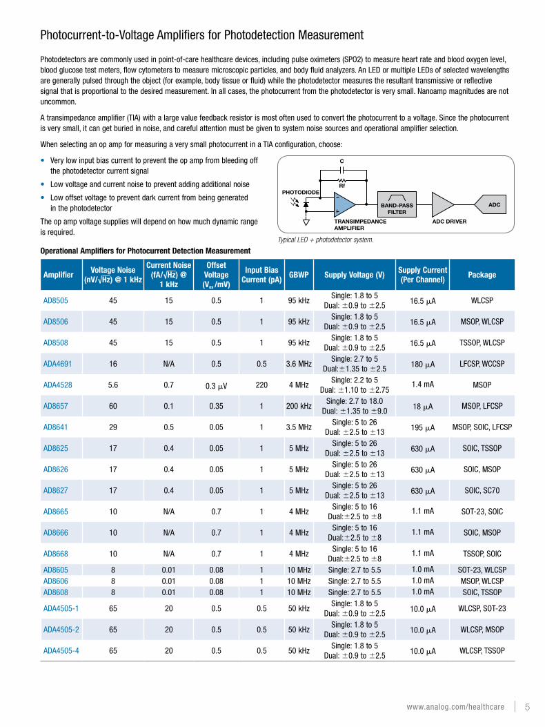
Photocurrent-to-Voltage Amplifiers for Photodetection Measurement
Photodetectors are commonly used in point-of-care healthcare devices, including pulse oximeters (SPO2) to measure heart rate and blood oxygen level, blood glucose test meters, flow cytometers to measure microscopic particles, and body fluid analyzers. An LED or multiple LEDs of selected wavelengths are generally pulsed through the object (for example, body tissue or fluid) while the photodetector measures the resultant transmissive or reflective signal that is proportional to the desired measurement. In all cases, the photocurrent from the photodetector is very small. Nanoamp magnitudes are not uncommon.
A transimpedance amplifier (TIA) with a large value feedback resistor is most often used to convert the photocurrent to a voltage. Since the photocurrent is very small, it can get buried in noise, and careful attention must be given to system noise sources and operational amplifier selection.
When selecting an op amp for measuring a very small photocurrent in a TIA configuration, choose:
• Very low input bias current to prevent the op amp from bleeding off the photodetector current signal
• Low voltage and current noise to prevent adding additional noise
• Low offset voltage to prevent dark current from being generated in the photodetector
The op amp voltage supplies will depend on how much dynamic range is required.
Operational Amplifiers for Photocurrent Detection Measurement
Amplifier Voltage Noise (nV/√Hz) @ 1 kHz
Current Noise (fA/√Hz) @
1 kHz
Offset Voltage (Vos /mV)
Input Bias Current (pA) GBWP Supply Voltage (V) Supply Current
(Per Channel) Package
AD8505 45 15 0.5 1 95 kHzSingle: 1.8 to 5
Dual: ±0.9 to ±2.5 16.5 μA WLCSP
AD8506 45 15 0.5 1 95 kHzSingle: 1.8 to 5
Dual: ±0.9 to ±2.5 16.5 μA MSOP, WLCSP
AD8508 45 15 0.5 1 95 kHzSingle: 1.8 to 5
Dual: ±0.9 to ±2.5 16.5 μA TSSOP, WLCSP
ADA4691 16 N/A 0.5 0.5 3.6 MHzSingle: 2.7 to 5
Dual:±1.35 to ±2.5 180 μA LFCSP, WCCSP
ADA4528 5.6 0.7 0.3 μV 220 4 MHzSingle: 2.2 to 5
Dual: ±1.10 to ±2.751.4 mA MSOP
AD8657 60 0.1 0.35 1 200 kHzSingle: 2.7 to 18.0
Dual: ±1.35 to ±9.0 18 μA MSOP, LFCSP
AD8641 29 0.5 0.05 1 3.5 MHzSingle: 5 to 26
Dual: ±2.5 to ±13 195 μA MSOP, SOIC, LFCSP
AD8625 17 0.4 0.05 1 5 MHzSingle: 5 to 26
Dual: ±2.5 to ±13 630 μA SOIC, TSSOP
AD8626 17 0.4 0.05 1 5 MHzSingle: 5 to 26
Dual: ±2.5 to ±13 630 μA SOIC, MSOP
AD8627 17 0.4 0.05 1 5 MHzSingle: 5 to 26
Dual: ±2.5 to ±13 630 μA SOIC, SC70
AD8665 10 N/A 0.7 1 4 MHzSingle: 5 to 16
Dual:±2.5 to ±81.1 mA SOT-23, SOIC
AD8666 10 N/A 0.7 1 4 MHzSingle: 5 to 16
Dual:±2.5 to ±81.1 mA SOIC, MSOP
AD8668 10 N/A 0.7 1 4 MHzSingle: 5 to 16
Dual:±2.5 to ±81.1 mA TSSOP, SOIC
AD8605 8 0.01 0.08 1 10 MHz Single: 2.7 to 5.5 1.0 mA SOT-23, WLCSPAD8606 8 0.01 0.08 1 10 MHz Single: 2.7 to 5.5 1.0 mA MSOP, WLCSP AD8608 8 0.01 0.08 1 10 MHz Single: 2.7 to 5.5 1.0 mA SOIC, TSSOP
ADA4505-1 65 20 0.5 0.5 50 kHzSingle: 1.8 to 5
Dual: ±0.9 to ±2.5 10.0 μA WLCSP, SOT-23
ADA4505-2 65 20 0.5 0.5 50 kHzSingle: 1.8 to 5
Dual: ±0.9 to ±2.5 10.0 μA WLCSP, MSOP
ADA4505-4 65 20 0.5 0.5 50 kHzSingle: 1.8 to 5
Dual: ±0.9 to ±2.5 10.0 μA WLCSP, TSSOP
Typical LED + photodetector system.
PHOTODIODE
TRANSIMPEDANCE AMPLIFIER
ADC DRIVER
ADC
Rf
C
BAND-PASSFILTER
www.analog.com/healthcare | 5
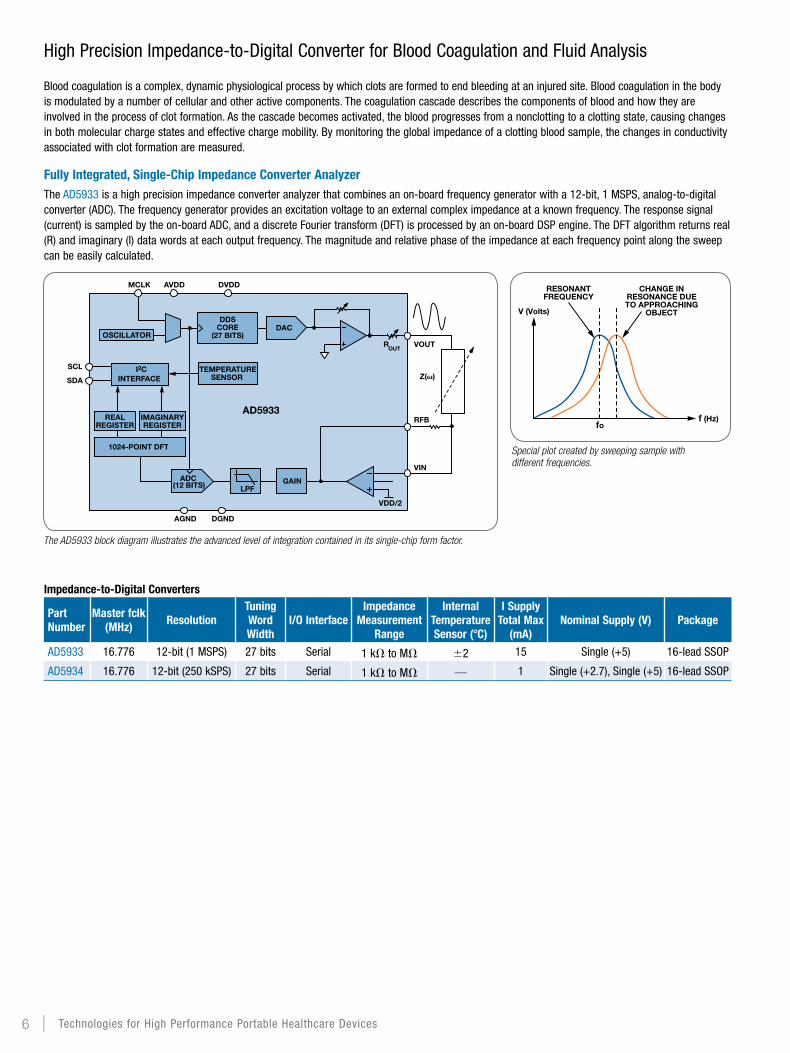
High Precision Impedance-to-Digital Converter for Blood Coagulation and Fluid Analysis
Blood coagulation is a complex, dynamic physiological process by which clots are formed to end bleeding at an injured site. Blood coagulation in the body is modulated by a number of cellular and other active components. The coagulation cascade describes the components of blood and how they are involved in the process of clot formation. As the cascade becomes activated, the blood progresses from a nonclotting to a clotting state, causing changes in both molecular charge states and effective charge mobility. By monitoring the global impedance of a clotting blood sample, the changes in conductivity associated with clot formation are measured.
Fully Integrated, Single-Chip Impedance Converter AnalyzerThe AD5933 is a high precision impedance converter analyzer that combines an on-board frequency generator with a 12-bit, 1 MSPS, analog-to-digital converter (ADC). The frequency generator provides an excitation voltage to an external complex impedance at a known frequency. The response signal (current) is sampled by the on-board ADC, and a discrete Fourier transform (DFT) is processed by an on-board DSP engine. The DFT algorithm returns real (R) and imaginary (I) data words at each output frequency. The magnitude and relative phase of the impedance at each frequency point along the sweep can be easily calculated.
Impedance-to-Digital Converters
Part Number
Master fclk (MHz) Resolution
Tuning Word Width
I/O InterfaceImpedance
Measurement Range
Internal Temperature Sensor (∙C)
I Supply Total Max
(mA)Nominal Supply (V) Package
AD5933 16.776 12-bit (1 MSPS) 27 bits Serial 1 kΩ to MΩ ±2 15 Single (+5) 16-lead SSOP
AD5934 16.776 12-bit (250 kSPS) 27 bits Serial 1 kΩ to MΩ — 1 Single (+2.7), Single (+5) 16-lead SSOP
V (Volts)
f (Hz)fo
RESONANTFREQUENCY
CHANGE INRESONANCE DUETO APPROACHING
OBJECT
Special plot created by sweeping sample with different frequencies.
The AD5933 block diagram illustrates the advanced level of integration contained in its single-chip form factor.
VDD/2
DAC
SCL
SDA
DVDDAVDDMCLK
AGND DGND
ROUT
VOUT
AD5933RFB
VIN
1024-POINT DFT
INTERFACE
IMAGINARYREGISTER
REALREGISTER
OSCILLATOR
DDSCORE
(27 BITS)
TEMPERATURESENSOR
ADC(12 BITS) LPF
GAIN
I2CZ()
6 | Technologies for High Performance Portable Healthcare Devices

Capacitive Sensing for Hermetically Sealed User Interfaces and Body Worn Sensor Contact
The human interface must also support a wide range of individuals with varied intellectual and physical capacities including eyesight, manual dexterity, and hearing. The interface also must offer smart, closed-loop, fail-safe features that will ensure proper, reliable, and safe device operation under all conditions.
Capacitive sensing is an ideal solution for developing a complete hermetically sealed device that is secure against the entry of water vapor and foreign bodies in order to maintain proper function levels and reliability under all conditions. Furthermore, a sealed capacitive sensing human interface eliminates the traditional mechanical buttons that are prone to collecting bacteria or subject to harsh cleaning liquids. Additional benefits of replacing traditional mechanical buttons with capacitive sensing include eliminating the mechanical buttons from the bill of materials and easier product assembly during product manufacturing.
It is often beneficial to have information about the quality of contact between the device’s surface area and the skin before the device is activated or a measurement is taken. The range of devices could include a medical probe that needs to rest flush on the skin, a biopotential electrode sensor, or the housing holding a catheter tube in place. To achieve this additional performance, several capacitive sensor electrodes, shown in green, could be embedded directly into the device’s plastic housing at the injection molding stage during manufacturing. Once the electrode information is available, a simple algorithm running on the host controller can be applied to determine if all sensor electrodes are making proper contact with the skin.
Selecting a Capacitive Sensor ControllerSelecting a capacitive sensor controller should start by selecting a controller that:
• Does not require external RC sensor tuning components.
• Includes an analog front end (AFE) that supports accurate measurements to detect the small energy on the capacitive sensors.
• Offers on-chip environmental tracking and calibration to correct for environmental baseline drift errors.
• Includes on-chip parasitic capacitance offset adjustment and low latency periods from touch to response.
Capacitive-to-Digital Controllers (CDCs)Part Number
Resolution (Bits) Rate (ms) Number of
ChannelsSupply Voltage
(V) Power Dissipation Input Base C (pF Max)
CIN Range (pF) Package
AD7148 16 9 8Multi (+3.3 analog,
+3.3 digital)3.3 mW = full power 71 μW = low power
20 ±8 LFCSP
AD7147A 16 9 13Single (+3),
Single (+3.3)3.3 mW = full power 71 μW = low power
20 ±8 LFCSP
AD7147 16 9 13Single (+3),
Single (+3.3)3.3 mW = full power 71 μW = low power
20 ±8 WLCSP
AD7156 12 10 2 1.8 to 3.60.25 mW = full power 0.7 μW = shut down
(3.6 V supplies)12.5 0.0 to 4.0 LFCSP
SENSOR OR PROBE HEAD
BODY WORN SENSOR
CALIBRATIONENGINE
SERIAL INTERFACEAND CONTROL LOGIC
CALIBRATIONRAM
POWER-ONRESET LOGIC
INTERRUPTAND GPIO
LOGIC
EXCITATIONSOURCE
ACSHIELD VCC GND BIAS
CONTROLAND DATAREGISTERS
16-BIT-CDC
SW
ITC
HM
AT
RIX
19CIN0
20CIN1
21CIN2
22CIN3
23CIN4
24CIN5
1CIN6
2CIN7
3CIN8
4CIN9
5CIN10
6CIN11
7CIN12
VDRIVE GPIO
8 11 10 9
1812
13 14 15 16 17
SDO/SDA
SDI/ADD0
SCLK CS/ADD1
INT
AD7147/AD7147A
www.analog.com/healthcare | 7
Low Power, High Performance Analog Interface
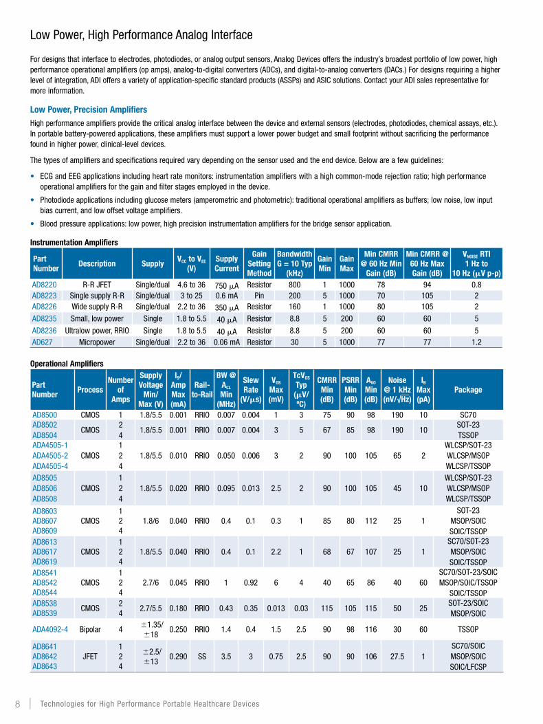
For designs that interface to electrodes, photodiodes, or analog output sensors, Analog Devices offers the industry’s broadest portfolio of low power, high performance operational amplifiers (op amps), analog-to-digital converters (ADCs), and digital-to-analog converters (DACs.) For designs requiring a higher level of integration, ADI offers a variety of application-specific standard products (ASSPs) and ASIC solutions. Contact your ADI sales representative for more information.
Low Power, Precision AmplifiersHigh performance amplifiers provide the critical analog interface between the device and external sensors (electrodes, photodiodes, chemical assays, etc.). In portable battery-powered applications, these amplifiers must support a lower power budget and small footprint without sacrificing the performance found in higher power, clinical-level devices.
The types of amplifiers and specifications required vary depending on the sensor used and the end device. Below are a few guidelines:
• ECG and EEG applications including heart rate monitors: instrumentation amplifiers with a high common-mode rejection ratio; high performance operational amplifiers for the gain and filter stages employed in the device.
• Photodiode applications including glucose meters (amperometric and photometric): traditional operational amplifiers as buffers; low noise, low input bias current, and low offset voltage amplifiers.
• Blood pressure applications: low power, high precision instrumentation amplifiers for the bridge sensor application.
Instrumentation Amplifiers
Part Number Description Supply VCC to VEE
(V)Supply Current
Gain Setting Method
Bandwidth G = 10 Typ
(kHz)
Gain Min
Gain Max
Min CMRR @ 60 Hz Min
Gain (dB)
Min CMRR @ 60 Hz Max Gain (dB)
VNOISE RTI 1 Hz to
10 Hz (𝛍V p-p) AD8220 R-R JFET Single/dual 4.6 to 36 750 μA Resistor 800 1 1000 78 94 0.8AD8223 Single supply R-R Single/dual 3 to 25 0.6 mA Pin 200 5 1000 70 105 2AD8226 Wide supply R-R Single/dual 2.2 to 36 350 μA Resistor 160 1 1000 80 105 2
AD8235 Small, low power Single 1.8 to 5.5 40 μA Resistor 8.8 5 200 60 60 5
AD8236 Ultralow power, RRIO Single 1.8 to 5.5 40 μA Resistor 8.8 5 200 60 60 5AD627 Micropower Single/dual 2.2 to 36 0.06 mA Resistor 30 5 1000 77 77 1.2
Operational Amplifiers
Part Number Process
Number of
Amps
Supply Voltage
Min/Max (V)
IS/Amp Max (mA)
Rail-to-Rail
BW @ ACL
Min (MHz)
Slew Rate
(V/𝛍s)
VOS Max (mV)
TcVOS Typ
(𝛍V/ºC)
CMRR Min (dB)
PSRR Min (dB)
AVO Min (dB)
Noise @ 1 kHz (nV/√Hz)
IB
Max (pA)
Package
AD8500 CMOS 1 1.8/5.5 0.001 RRIO 0.007 0.004 1 3 75 90 98 190 10 SC70AD8502 AD8504
CMOS2 4
1.8/5.5 0.001 RRIO 0.007 0.004 3 5 67 85 98 190 10 SOT-23 TSSOP
ADA4505-1 ADA4505-2 ADA4505-4
CMOS1 2 4
1.8/5.5 0.010 RRIO 0.050 0.006 3 2 90 100 105 65 2WLCSP/SOT-23 WLCSP/MSOP WLCSP/TSSOP
AD8505 AD8506 AD8508
CMOS1 2 4
1.8/5.5 0.020 RRIO 0.095 0.013 2.5 2 90 100 105 45 10WLCSP/SOT-23 WLCSP/MSOP WLCSP/TSSOP
AD8603 AD8607 AD8609
CMOS1 2 4
1.8/6 0.040 RRIO 0.4 0.1 0.3 1 85 80 112 25 1SOT-23
MSOP/SOIC SOIC/TSSOP
AD8613 AD8617 AD8619
CMOS1 2 4
1.8/5.5 0.040 RRIO 0.4 0.1 2.2 1 68 67 107 25 1SC70/SOT-23 MSOP/SOIC SOIC/TSSOP
AD8541 AD8542 AD8544
CMOS1 2 4
2.7/6 0.045 RRIO 1 0.92 6 4 40 65 86 40 60SC70/SOT-23/SOIC MSOP/SOIC/TSSOP
SOIC/TSSOPAD8538 AD8539
CMOS2 4
2.7/5.5 0.180 RRIO 0.43 0.35 0.013 0.03 115 105 115 50 25SOT-23/SOIC MSOP/SOIC
ADA4092-4 Bipolar 4 ±1.35/ ±18
0.250 RRIO 1.4 0.4 1.5 2.5 90 98 116 30 60 TSSOP
AD8641 AD8642 AD8643
JFET1 2 4
±2.5/ ±13
0.290 SS 3.5 3 0.75 2.5 90 90 106 27.5 1SC70/SOIC MSOP/SOIC SOIC/LFCSP
8 | Technologies for High Performance Portable Healthcare Devices

Low Power, High Performance Analog Interface (Continued)
In addition to some of the amplifiers listed in the table, designers can select op amps by parameters, find expert system-level advice on design problems with our amplifier reference circuits (Circuits from the Lab™), and download design tools, selection guides, calculators, and SPICE models at www.analog.com/amplifiers.
Data Converters As the world’s leading provider of data converters, Analog Devices offers digital-to-analog and analog-to-digital converters from 8 bits to 24 bits. ADI converters are unmatched in their ability to deliver performance and value, and they are supported by design tools and technical documentation engineers need to accelerate time to market. Whether the data conversion challenge is high speed or precision, engineers will find an ADC or DAC to suit every specification: accuracy, resolution, sample rate, bandwidth, power, size, and value.
Low Voltage Precision Digital-to-Analog Converters (DACs)Part Number Channels Bits On-Chip Reference (V) Interface PackageAD5320 1 12 No SPI SOT-23, MSOP
AD5621 1 12 No SPI SC70
AD5622 1 12 No I2C SC70
AD5620 1 12 1.25/2.5 SPI SOT-23, MSOP
AD5640 1 14 1.25/2.5 SPI SOT-23, MSOP
AD5660 1 16 1.25/2.5 SPI SOT-23, MSOP
AD5322 2 12 No SPI MSOP
AD5623R 2 12 1.25/2.5 SPI LFCSP, MSOP
AD5627R 2 12 1.25/2.5 I2C LFCSP, MSOP
AD5643R 2 14 1.25/2.5 SPI MSOP
AD5663R 2 16 1.25/2.5 SPI LFCSP, MSOP
AD5324 4 12 No SPI LFCSP, MSOP
AD5624R 4 12 1.25/2.5 SPI LFCSP, MSOP
AD5625R 4 12 1.25/2.5 I2C LFCSP, TSSOP
AD5644R 4 14 1.25/2.5 SPI LFCSP, MSOPAD5664R 4 16 1.25/2.5 SPI LFCSP, MSOP
Analog-to-Digital Converters (ADCs)Part Number
Resolution (Bits) Channels INL
(Typ)THD (dB) Throughput Supply (V) Power Dissipation Package
AD7298 12 8 ±0.5 LSB
–82 @ 50 kHz
1 MSPSAnalog: 2.8 to 3.6 Digital: 1.65 to 3.6
17.4 mW LFCSP (QFN)
AD7476A 12 1 ±0.75 LSB
–80 @ 100 kHz
1 MSPSAnalog: 2.35 to 5.25 Digital: 2.35 to 5.25
3.6 mW SC70, MSOP
AD7476 12 1 ±0.6 LSB
–80 @ 100 kHz
1 MSPSAnalog: 2.35 to 5.25 Digital: 2.35 to 5.25
3.6 mW SOT-23
AD7942 14 1 ±0.4 LSB
–100 @ 20 kHz
250 kSPSAnalog: 2.3 to 5.5 Digital: 1.8 to 5.0
1.25 mW @ 2.5 V/100 kSPS 3.6 mW @ 5 V/100 kSPS
1.25 μW @ 2.5 V/100 SPS
MSOP, QFN (LFCSP)
AD7171 16 1 ±0.4 LSB
N/A 125 Hz 2.7 to 5.25 0.33 mW LFCSP
AD7980 16 1 ±0.6 LSB
–110 @ 10 kHz
1 MSPSAnalog: 2.5 to 5.0 Digital: 1.8 to 5.0
7.0 mW @ 1 MSPS 70 μW @ 10 kSPS
MSOP, QFN (LFCSP)
AD7685 16 1 ±0.6 LSB
–110 @ 20 kHz
250 kSPSAnalog: 2.3 to 5.5 Digital: 1.8 to 5.0
1.4 μW @ 2.5 V/100 SPS 1.35 mW @ 2.5 V/100 kSPS
4 mW @ 5 V/100 kSPS
MSOP, QFN (LFCSP)
AD7682/AD7689
16 4/8 ±0.4 LSB
–100 @ 20 kHz
250 kSPSAnalog: 2.3 to 5.5 Digital: 1.8 to 5.5
3.5 mW @ 2.5 V/200 kSPS 12.5 mW @ 5 V/250 kSPS
LFCSP
AD7986 18 1 ±0.6 LSB
–115 @ 20 kHz
2 MSPS (TURBO = high), 1.5 MSPS (TURBO = low)
Analog: 2.3 to 2.6 Digital: 1.8 to 2.7
15 mW @ 2 MSPS, with external reference
26 mW @ 2 MSPS, with internal reference
QFN (LFCSP)
AD7767 24 1 ±3 ppm
–115 @ 1 kHz
32 kSPS 64 kSPS
128 kSPS
Analog: 2.3 to 2.6 Digital: 1.8 to 3.6
8.5 mW @ 32 kSPS (AD7767-2) 10.5 mW @ 64 kSPS (AD7767-1)
15 mW @ 128 kSPS (AD7767)TSSOP
www.analog.com/healthcare | 9

Low Power, High Performance Analog Interface (Continued) Data Conversion Knowledge Resource
Analog Devices’ Data Conversion Knowledge Resource is an easy-to-navigate library of in-depth technical material focusing on key aspects of conversion stage design. Clicking on the individual blocks within the Data Conversion Knowledge Resource home page diagram serves up design and applications engineering content relevant to that specific subject.
Put ADI’s 45 year span of pioneering work in data conversion to work for you. Visit the Data Conversion Knowledge Resource for design-relevant handbooks, applications notes, tutorials, webcasts, tools, and more at www.analog.com/theKnowledgeResource.
Voltage References ADI’s precision micropower voltage reference products provide class-leading specification in an affordable budget. These parts feature ≤±0.1% initial accuracy, low operating current, and low output noise in small packages, ideal for battery-operated portable devices.
Precision Voltage References
Part Number Output Voltage (V) Initial Accuracy (%) Operating Current Tempco
(ppm/∙C)0.1 Hz to 10 Hz Noise (𝛍V p-p) Package
ADR3425 2.5 0.1 100 μA max 8 18 SOT-23
AD1580 1.225 0.08, 0.8 50 μA to 10 mA 50, 100 5 SC70/SOT-23
ADR5043 3 0.1, 0.2 50 μA to 15 mA 75, 100 25.8 SC70/SOT-23
Small, Highly Accurate Temperature Sensing
ADI’s high performance digital temperature sensors measure temperature to an accuracy of ±0.25°C over a range of –20°C to +105°C and ±0.5°C from –40°C to +125°C. These devices offer breakthrough accuracy and a high level of integration offering designers an alternative to thermistors and the peripheral parts these devices require. There is no extra signal processing, characterization, or calibration required. The sensors offer stable and reliable temperature measurement with a typical drift specification of ±0.0072°C and repeatability of ±0.015°C
Digital Temperature Sensors
Part Number Temperature Resolution (°C/LSB)
25°C Temperature Error (°C)
Resolution (Bits)
Serial Interface
Temperature Range (∙C)
Supply Voltage Range (V) Package
ADT7310 0.0078°C 0.5 16 SPI –55 to +150 +2.7 to +5.5 SOIC
ADT7320 0.0078°C 0.0017 16 SPI –40 to +150 +2.7 to +5.5 LFCSP
ADT7410 0.0078°C 0.5 16 I2C –55 to +150 +2.7 to +5.5 SOIC
ADT7420 0.0078°C 0.2 16 I2C –40 to +150 +2.7 to +5.5 LFCSP
10 | Technologies for High Performance Portable Healthcare Devices

Low Power, Low Cost Precision Analog Microcontrollers and Digital Signal Processors
Analog Devices has an extensive portfolio of digital signal processors (DSPs) and analog microcontrollers for portable home healthcare device design requirements.
Precision Analog Microcontroller: ARM Cortex-M3 with ISM Band Transceiver For those portable home healthcare designs requiring a high level of integration, the ADuCRF101 system on a chip (SoC) integrates high performance converter technology, an ARM Cortex-M3 processor, on-chip memory, and the added functionality of an RF transceiver for wireless communications on a single chip. It offers low operating power (190 μA/MHz) and can power down to under 1.6 μA with a state retained, making it ideal for mains and battery operated medical devices, including infusion pumps and vital sign monitors.
ADuCRF101 Features
• High performance ISM band RF transceiver
• ARM Cortex-M3 32-bit RISC MCU, 128 kB Flash/EE memory, 16 kB RAM
• Operates directly from 3.6 V battery
• 6-channel, 14-bit, 500 kSPS SAR ADC
• 9 mm × 9 mm, 64-lead LFCSP
Precision Analog Microcontrollers with 12-Bit ARM7TDMI MCU Analog Devices precision analog microcontrollers combine precision analog functions, such as high resolution ADCs and DACs, voltage reference, temperature sensor, and a host of other peripherals, with an industry-standard microcontroller and flash memory. The ADuC712x ARM7TDMI® family integrates 12-bit ADCs, 12-bit DACs, flash, SRAM, and a host of digital peripherals designed for medical applications.
Precision Analog MicrocontrollersPart Number MCU Core MCU Speed
(MIPS)Flash (kB)
SRAM (kB)
GPIO Pins
Resolution (Bits)
ADC Speed (kSPS)
ADC Channels Other 12-Bit DAC
OutputsADuC7021 ARM7TDMI 40 62 8 13 12 1000 8 — 2
ADuC7022 ARM7TDMI 40 62 8 13 12 1000 10 — —
ADuC7024 ARM7TDMI 40 62 8 30 12 1000 10 PWM 2
ADuC7025 ARM7TDMI 40 62 8 30 12 1000 12 PWM —
ADuC7026 ARM7TDMI 40 62 8 40 12 1000 12 PWM 4
ADuC7027 ARM7TDMI 40 62 8 40 12 1000 16 PWM —
ADuC7028 ARM7TDMI 40 62 8 40 12 1000 8 — 4
ADuC7124 ARM7TDMI 40 128 32 40 12 1000 16 PWM 4
ADuCRF101 Cortex-M3 20 128 16 28 14 500 6 PWM, radio, DMA —
Digital Signal ProcessorsThe ADSP-BF52x and ADSP-BF592 Blackfin® processors deliver the computational power required for fast, accurate results for in-home medical systems, including wearable monitoring devices and portable diagnostic systems. In addition to providing the signal processing for real-time analysis, Blackfin processors can provide control of the user interface (LCD, button, touch screen). A range of connectivity options (network wired/wireless, USB) are available to enable the transfer of data from device to patient and doctor.
ADuCRF101 functional block diagram.
LFXTAL1
LFXTAL2
ADC0
LVDD
AVDD
RFIO_1P
RFIO_1N
ADC5
RFO2
UHF TRANSCEIVER
IOVDD
XOSC26P
XOSC26N
GPIOS
14-BIT SARADC 500kSPS
BAND GAPREFERENCE
PORRESET
OSC
PACKET HANDLERAND WAKE UP CONTROL
LOWPOWERRADIO
2 × GENERAL PURPOSE TIMERS
WAKE-UPTIMER
INTERRUPTCONTROLLER
SERIALWIRE SPI I2C UART PWM GPIOS
2 KBYTES
16K BYTESSRAM
(4k × 32 BITS)
128 KBYTESFLASH/EE
(32k × 32 BITS)
WATCHDOG TIMER
MUX
TEMPSENSOR
ADuCRF101
VREFARM CORTEX M3-BASED MCU
WITH ADDITIONAL PERIPHERALS
ADuC7124 functional block diagram.
1MSPS12-BIT ADC
DAC0
DAC1
DAC2
DAC3
PWMEXTERNALMEMORY
INTERFACE
ADuC7124/ADuC7126
ADC0
XCLKI
XCLKO
RST
VREF
ADC15
MUX
TEMPSENSOR
BAND GAPREF
OSCAND PLL
PSM
POR
CMP0
CMP1
CMPOUT
PLA
VECTOREDINTERRUPT
CONTROLLER
4 GENERAL-PURPOSE TIMERS
8k × 32 SRAM63k × 16 FLASH/EEPROM
SPI, 2 × I2C,2 × UART
GPIO
JTAG
ARM7TDMI-BASED MCU WITHADDITIONAL PERIPHERALS
12-BITDAC
12-BITDAC
12-BITDAC
12-BITDAC
www.analog.com/healthcare | 11

Reliable Wireless Communication for Transfer of Data
To maximize patient comfort and mobility, wireless connectivity is becoming ubiquitous. Open standards such as Bluetooth and Zigbee provide low cost options for those applications with multiple band requirements, including the 2.4 GHz band. For near-body or body worn sensors, the sub-1 GHz ISM band offers an alternative and can provide maximum design flexibility, including the ability to trade off range against power, optimize data security, and minimize software and memory overhead. To address applications utilizing ISM bands, ADI offers standalone transceivers, as well as a fully integrated system on a chip (SoC) solution.
Low Power ISM Band TransceiversThe ADF7023 is a low power, high performance, highly integrated 2FSK/GFSK/OOK/MSK/GMSK transceiver designed for operation in the 862 MHz to 928 MHz and 431 MHz to 464 MHz frequency bands, which cover the worldwide license-free ISM bands at 433 MHz, 868 MHz, and 915 MHz. It is suitable for circuit applications that operate under the European ETSI EN 300-220, the North American FCC (Part 15), the Chinese short-range wireless regulatory standards, or other similar regional standards. Data rates from 1 kbps to 300 kbps are supported.
ADF7023 Features
• Frequency bands
• 862 MHz to 928 MHz
• 431 MHz to 464 MHz
• Data rates supported: 1 kbps to 300 kbps
• 1.8 V to 3.6 V power supply
• Single-ended and differential PAs
• Low IF receiver with programmable IF bandwidths: 100 kHz, 150 kHz, 200 kHz, 300 kHz
RSSI/LOGAMP
LNA
ADCIN_ATB3
SCLKMOSI
1GPIO REFERS TO PINS 17, 18, 19, 20, 25, AND 27.
MISOCS
IRQ_GP3
RFIO_1PRFIO_1N
RFO2
SPI
IRQ CTRL
FSKASK
DEMOD
CDRAFCAGC
4kB ROM MAC
256 BYTEPACKET
RAM
2kB RAM
8-BIT RISC
PROCESSOR
BIAS 26MHz OSCL
DO
4
LD
O3
LD
O2
LD
O1
TIMER UNIT
64 BYTEBBRAM
TEMP SENSOR
BATTERY MONITOR
CLOCK DIVIDER
GPIO
TEST DAC
ANALOG TEST
PA RAMPPROFILE
PA
MU
X 8-BIT ADC
LOOPFILTER
CHARGEPUMP
PFD 26MHz OSC
DIVIDER
- MODULATOR
GAUSSIAN FILTER
fDEV
32kHz RCOSC
32kHz OSC
PA
ADF7023
256 BYTEMCR RAM GPIO1
DIVIDER
XOSC26N XOSC26PXOSC32KP_GP5_ATB1XOSC32KN_ATB2RBIASCREGRFx CREGVCO CREGSYNTH CREGDIGx
WAKE-UP CONTROL
ADF7023 functional block diagram.
ISM Band Transceiver with Microcontroller System on a Chip (SoC)
The ADuCRF101 is a fully integrated SoC solution that includes an energy efficient 431 MHz to 464 MHz and 862 MHz to 928 MHz internal UHF transceiver, low power ARM Cortex-M3 core, and Flash/EE memory. The transceiver consumes only 12.8 mA in receive mode, while maintaining a typical sensitivity of –107.5 dB at 38.4 kbps (2FSK). The transmit mode is equally efficient, with supply current as low as 9 mA, depending on the user programmed RF power level. The device operates directly from a 3.6 V battery and utilizes an autonomous packet handler to minimize system current consumption during wireless communications.
RF Transceivers
Part Number Frequency Range (MHz)
Modulation Mode
Max Data Rate
Phase Noise Floor
(dBc/Hz)
Tx Current for
0 dBm (mA)
Rx Current
(mA)
Rx Sensitivity
(dBm)
Min Pos Supply
(V)
Max Pos Supply
(V)
Output Power (dBm)
Package
ADF7023431 to 464, 862 to 928
GFSK/FSK/MSK, GMSK, OOK
300 kbps
196 13 12.8 116 1.8 3.6–16 to +13.5
32-lead LFCSP
ADF72422400 to 2483.5
DSSS-OQPSK, FSK/GFSK
2 Mbps 145 19.6 19 — 1.8 3.6–20 to +4.8
32-lead LFCSP
ADuCRF101431 to 464, 862 to 928
GFSK/FSK/MSK, GMSK, OOK
300 kbps
196 13 12.8 116 1.8 3.6–16 to +13.5
64-lead LFCSP
12 | Technologies for High Performance Portable Healthcare Devices
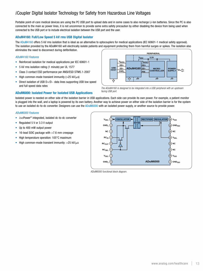
iCoupler Digital Isolator Technology for Safety from Hazardous Line Voltages
Portable point-of-care medical devices are using the PC USB port to upload data and in some cases to also recharge Li-Ion batteries. Since the PC is also connected to the main ac power lines, it is not uncommon to provide some extra safety precaution by either disabling the device from being used when connected to the USB port or to include electrical isolation between the USB port and the user.
ADuM4160: Full/Low Speed 5 kV rms USB Digital Isolator The ADuM4160 offers 5 kV rms isolation that is ideal as an alternative to optocouplers for medical applications (IEC 60601-1 medical safety approval). The isolation provided by the ADuM4160 will electrically isolate patients and equipment protecting them from harmful surges or spikes. The isolation also eliminates the need to disconnect during defibrillation.
ADuM4160 Features
• Reinforced isolation for medical applications per IEC 60601-1
• 5 kV rms isolation rating (1 minute) per UL 1577
• Class 3 contact ESD performance per ANSI/ESD STM5.1-2007
• High common-mode transient immunity (>25 kV/μs)
• Direct isolation of USB D+/D− data lines supporting USB low speed and full speed data rates
ADuM6000: Isolated Power for Isolated USB ApplicationsIsolated power is needed on either side of the isolation barrier in USB applications. Each side can provide its own power. For example, a patient monitor is plugged into the wall, and a laptop is powered by its own battery. Another way to achieve power on either side of the isolation barrier is for the system to use an isolated dc-to-dc converter. Designers can use the ADuM6000 with an isolated power supply, or another source to provide power.
ADuM6000 Features
• isoPower® integrated, isolated dc-to-dc converter
• Regulated 5 V or 3.3 V output
• Up to 400 mW output power
• 16-lead SOIC package with >7.6 mm creepage
• High temperature operation: 105°C maximum
• High common-mode transient immunity: >25 kV/μs
The ADuM4160 is designed to be integrated into a USB peripheral with an upstream facing USB port.
USBHOST
VBUS1 VBUS2
DD+DD–
GND1
DD+
3.3VVDD2
DD–PIN
MICRO-CONTROLLER
PERIPHERAL
POWERSUPPLY
ADuM4160
VDD1
GND1
NC
RCIN
RCOUT
RCSEL
VDD1
ATOR
GND1
VISO
GNDISO
NC
VSEL
NC
NC
VISO
GNDISO
1
2
3
4
5
6
7
8
16
15
14
13
12
11
10
9ADuM6000
REGULATOROSCILL RECTIFIER
ADuM6000 functional block diagram.
www.analog.com/healthcare | 13

High Efficiency Power Management for Battery Operated Devices
Standard lithium coin cell batteries used in point-of-care healthcare devices provide a typical output voltage in the range of 2.0 V to 3.0 V. Some high performance portable systems are also powered by rechargeable Li-Ion batteries with a 3.0 V to 4.2 V output. The two main design challenges with battery operated systems with regards to power are the battery life and the battery output voltage.
Battery life can be extended by selecting components with very low quiescent and shutdown currents and by keeping the main power consuming devices, such as the host processor, in a sleep state as much as possible. The battery output level has to comply with all the IC operating voltages in the system, generally consisting of a mixture of components developed on different processes, thus different compliance voltages.
ICs used for high performance portable devices operate on a wide range of voltage rails. Even if all of the ICs can operate directly off the battery, some form of regulation, such as step-up regulator, step-down regulator, or both, will be required to maintain the highest system efficiency and longest battery life.
Linear Regulators
Part Number Description VOUT (V) IOUT Max (mA)
VIN Range VMIN to VMAx
Supply Current
(𝛍A)
VDROPOUT @ Rated IOUT (mV) Package
ADP121 CMOS, low quiescent 9 options: 1.2 to 3.3 150 2.5 to 5.5 40 90 to 120 WLCSP, TSOTADP122 CMOS, low quiescent 7 options: 2.5 to 3.3 300 2.3 to 5.5 45 85 LFCSPADP125 CMOS, 0.8 to 5 V N/A 500 2.3 to 5.5 45 130 LFCSPADP150 CMOS, ultralow noise 7 options: 1.8 to 3.3 150 2.2 to 5.5 10 105 WLCSP, TSOTADP170 CMOS, low dropout 5 options: 1.2 to 2.8 300 1.6 to 3.6 260 66 TSOTADP220 Dual, low noise, high PSRR 7 options: 1.2 to 2.8 200 2.5 to 5.5 220 150 WLCSP
Switching DC-to-DC Regulators
Part Number Description VIN Range (V) VOUT Options (V) IOUT
Max (A)
ISW Peak (A)
Supply Current (𝛍A)
Switch Frequency Package
ADP1612 Step-up 1.8 to 5.5 VIN to 20, adjustable — 1.4 1350650 kHz, 1.3 MHz
MSOP
ADP2108 Synchronous step-down 2.3 to 5.51.0, 1.1, 1.2, 1.3, 1.5, 1.82,
1.8, 2.3, 2.5, 3.0, 3.30.6 1.3 30 3 MHz WLCSP
ADP2138 Synchronous step-down 2.3 to 5.5 8 options: 0.8 to 3.3 0.8 1.5 30 3 MHz WLCSP
ADP2139Synchronous step-down
with load discharge switch2.3 to 5.5 8 options: 0.8 to 3.3 0.8 1.5 30 3 MHz WLCSP
ADP2504 Synchronous buck-boost 2.3 to 5.5 2.8, 3.3, 3.5, 4.2, 4.5, 5.0 1 1.3 50 2.5 MHz LFCSP
Multioutput Regulators
Part Number Product Description VIN Range (V) Number of Outputs
Switching Frequency (MHz)
Buck (mA)
LDO (mA) Key Features Package
ADP2140Low quiescent current buck converter with
300 mA LDO regulator
2.3 to 5.5 (LDO: 1.7 to 5.5)
2 3 600 300Auto sequence;
power goodLFCSP
ADP5020 General-purpose PMU 2.4 to 5.5 3 3 300, 600 150I2C, programmable
outputsLFCSP
ADP5022Dual buck regulator with 150 mA LDO
2.4 to 5.5 3 3 150, 500 150 — WLCSP
ADP5025System PMU
for digital still cameras2.45 to 5.5 9 2.5 700, 900 50
I2C, RTC, back-batt charger
WLCSP
ADP5030Dual LDO (VOUT = 1.2 V, 2.8 V)
with load switch 2.5 to 5.5 3 — —
200, 200
Load switch and level shifters
WLCSP
14 | Technologies for High Performance Portable Healthcare Devices

High Efficiency Power Management for Battery Operated Devices (Continued)
Display Backlight ControllersADI backlight drivers (controllers) are appropriate for display backlighting, keypad control, and status indicators. They extend battery life by reducing processor interaction and ambient light sensing (ALS) complexity. These intelligent state-machine products improve battery life by reducing processor interaction and improve time to market by reducing software complexities. User interface is also enhanced by the on-chip built-in controllers for automatic light adjustment based on ambient conditions.
Backlight Controllers
Part Number Description LED
NumberLED
Configuration Topology Application I2C Support
Max IOUT
(mA)
Brightness Control
Peak Efficiency
(%)
Switching Frequency
(MHz)ADP5501 WLED driver with ALS, RGB 6 Serial Inductive Backlighting Yes 30 I2C — 1ADP5520 WLED driver with ALS, RGB, KBRD 6 Serial Inductive Backlighting Yes 30 I2C — 1ADP8860 WLED driver with ALS 7 Parallel Capacitive Backlighting Yes 60 I2C 89 1ADP8861 WLED driver 7 Parallel Capacitive Backlighting Yes 60 PWM 89 1.32ADP8863 Fun lighting LED driver 7 Parallel Capacitive Backlighting Yes 60 I2C 89 1.32ADP8870 WLED driver with ALS and CABC 7 Parallel Capacitive Backlighting Yes 60 I2C 89 1.2
For More Information
Visit Our Healthcare Website
Additional healthcare device design resources and tools, including signal chains, recommended products, application notes, webcasts, technical articles, and more, are available at www.analog.com/healthcare.
Subscribe to Our Healthcare eNewsletter
The “Stay Tuned” healthcare eNewsletter, intended for the healthcare design engineer, will keep you informed of the latest products and tools available from ADI.
Subscribe today at www.analog.com/subscribe.
www.analog.com/healthcare | 15

i2C refers to a communications protocol originally developed by Philips Semiconductors (now NXP Semiconductors).
©2011 Analog Devices, inc. All rights reserved. Trademarks and registered trademarks are the property of their respective owners.
AH09519-0-11/11(A)www.analog.com/healthcare
Analog Devices, Inc.Worldwide HeadquartersAnalog Devices, Inc. One Technology Way P.O. Box 9106 Norwood, MA 02062-9106 U.S.A. Tel: 781.329.4700 (800.262.5643, U.S.A. only) Fax: 781.461.3113
Analog Devices, Inc. Europe HeadquartersAnalog Devices, Inc. Wilhelm-Wagenfeld-Str. 6 80807 Munich Germany Tel: 49.89.76903.0 Fax: 49.89.76903.157
Analog Devices, Inc. Japan HeadquartersAnalog Devices, KK New Pier Takeshiba South Tower Building 1-16-1 Kaigan, Minato-ku, Tokyo, 105-6891 Japan Tel: 813.5402.8200 Fax: 813.5402.1064
Analog Devices, Inc. Southeast Asia HeadquartersAnalog Devices 22/F One Corporate Avenue 222 Hu Bin Road Shanghai, 200021 China Tel: 86.21.2320.8000 Fax: 86.21.2320.8222