Technical Final Report
19
UC Berkeley Basic Science Title Toward ZnO Light Emitting Diode Permalink https://escholarship.org/uc/item/74r8z09z Author Liu, Jianlin Publication Date 2008-07-01 eScholarship.org Powered by the California Digital Library University of California
Transcript of Technical Final Report

UC BerkeleyBasic Science
TitleToward ZnO Light Emitting Diode
Permalinkhttps://escholarship.org/uc/item/74r8z09z
AuthorLiu, Jianlin
Publication Date2008-07-01
eScholarship.org Powered by the California Digital LibraryUniversity of California

Fundamental Science of Energy 009
"Toward ZnO Light Emitting Diode"
Jianlin Liu
July 2008
This paper is part of the University of California Energy Institute's (UCEI) Fundamental Science of Energy Working Paper Series. UCEI is a multi-campus research unit of the University of California located on the Berkeley campus.
UC Energy Institute 2547 Channing Way, # 5180
Berkeley, California 94720-5180 www.ucei.berkeley.edu

This report was issued in order to disseminate results of and information about energy research at the University of California campuses. Any conclusions or opinions expressed are those of the authors and not necessarily those of the Regents of the
University of California, the University of California Energy Institute or the sponsors of the research. Readers with further interest in or questions about the subject matter of the
report are encouraged to contact the authors directly.

Proposal Title: “Toward ZnO Light Emitting Diode”
Sponsor:
UC Energy Institute
Principal Investigator: Jianlin Liu
Department of Electrical Engineering University of California at Riverside, Riverside, CA92521
Email: [email protected]: (951)827-7131 Fax: (951)787-2425
1

1. Technical report The project scope focuses on developing reliable p-type ZnO semiconductor materials by
using plasma-assisted MBE and demonstrating feasibility of using ZnO-based materials
for solid-state lighting, including fabrication, test and evaluation of proof-of-concept ZnO
homo-junction LED devices. Over the two-year period July 1, 2006-June 30, 2008), we
have worked on this project extensively and achieved the following research results:
1. Low-resistivity Au/Ni Ohmic contacts to Sb-doped p-type ZnO ZnO is a wide band gap semiconductor material that has drawn a lot of attention
recently. However, p-type doping is extremely difficult due to the presence of native
defects and donors [U. Ozgur, Ya. I. Alivov, C. Liu, A. Teke, M. A. Reshchikov, S.
Dogan, V. Avrutin, S. J. Cho, and H. Morkoc, J Appl Phys 98, 041301 (2005). S. J.
Pearton, D. P. Norton, K. Ip, and Y. W. Heo, J. Vac. Sci. Technol. B 22, 932 (2004). D.
C. Look, Mater. Sci. Eng. B 80, 383 (2001)]. Active research is currently carried out to
explore various suitable p-type dopants for ZnO [A. Tsukazaki, A. Ohtomo, T. Onuma,
M. Ohtani, T. Makino, M. Sumiya, K. Ohtani, S. F. Chichibu, S. Fuke, Y. Segawa, H.
Ohno, H. Koinuma, and M. Kawasaki, Nat. Mater. 4, 42 (2005). D. K. Hwang, H. S. Kim,
J. H. Lim, J. Y. Oh, J. H. Yang, S. J. Park, K. K. Kim, D. C. Look, and Y. S. Park, Appl.
Phys. Lett. 86, 151917 (2005). Y. R. Ryu, T. S. Lee, and H. W. White, Appl. Phys. Lett.
83, 87 (2003). F. X. Xiu, Z. Yang, L. J. Mandalapu, J. L. Liu, and W. P. Beyermann,
Appl. Phys. Lett. 88, 052106 (2006). F. X. Xiu, Z. Yang, L. J. Mandalapu, and J. L. Liu,
Appl. Phys. Lett. 88, 152116 (2006). F. X. Xiu, Z. Yang, L. J. Mandalapu, D. T. Zhao, J.
L. Liu, and W. P. Beyermann, Appl. Phys. Lett. 87, 152101 (2005)]. Recently, Sb-doped
ZnO films grown on Si (100) substrates exhibited reliable and reproducible p-type
2

behavior [F. X. Xiu, Z. Yang, L. J. Mandalapu, J. L. Liu, and W. P. Beyermann, Appl.
Phys. Lett. 88, 052106 (2006). F. X. Xiu, Z. Yang, L. J. Mandalapu, and J. L. Liu, Appl.
Phys. Lett. 88, 152116 (2006). F. X. Xiu, Z. Yang, L. J. Mandalapu, D. T. Zhao, J. L. Liu,
and W. P. Beyermann, Appl. Phys. Lett. 87, 152101 (2005). F. X. Xiu, Z. Yang, L. J.
Mandalapu, D. T. Zhao, and J. L. Liu, Appl. Phys. Lett. 87, 252102 (2005).]. ZnO hetero-
and homo-junction devices were fabricated based on Sb-doped p-type ZnO films [L. J.
Mandalapu, F. X. Xiu, Z. Yang, and J. L. Liu, Appl. Phys. Lett. 88, 112108 (2006). L. J.
Mandalapu, Z. Yang, F. X. Xiu, and J. L. Liu, Appl. Phys. Lett. 88, 092103 (2006).],
where Al/Ti metal was used for achieving Ohmic contacts to both n-type and p-type ZnO.
However, relatively high contact resistance was observed for Al/Ti contacts on p-type
ZnO, which limited our device performance. There are several reports on various metal
schemes that have been employed for p-type ZnO films [J. H. Lim, K. K. Kim, D. K.
Hwang, H. S. Kim, J. Y. Oh, and S. J. Park, J. of Electrochem. Soc. 152, G179 (2005) S.
Kim, B. S. Kang, F. Ren, Y. W. Heo, K. Ip, D. P. Norton, and S. J. Pearton, Appl. Phys.
Lett. 84, 1904 (2004). H. S. Yang, Y. Li, D. P. Norton, K. Ip, S. J. Pearton, S. Jang, and F.
Ren, Appl. Phys. Lett. 86, 192103 (2005). K. Ip, G. T. Thaler, H. Yang, S. Y. Han, Y. Li,
D. P. Norton, S. J. Pearton, S. Jang, and F. Ren, J. Cryst. Growth 287, 149 (2006). S. H.
Kang, D. K. Hwang, and S. J. Park, Appl. Phys. Lett. 86, 211902 (2005)]. In this letter,
we explore Au/Ni metal for making Ohmic contacts to Sb-doped p-type ZnO films.
Sb-doped ZnO films were grown on n-Si(100) substrates at 550 ˚C using a
Perkin-Elmer MBE system. Prior to growth, the Si substrates were cleaned by the
Piranha-HF method and dried by nitrogen, which was followed by thermal cleaning at
650 ˚C. A thin undoped ZnO buffer layer was grown to improve the crystalline quality of
3

the subsequent Sb-doped ZnO layer. Undoped layer was grown for 30 mins while the
growth of Sb-doped layer was for 150 mins, giving rise to an effective thickness of about
435 nm. Sb-doped ZnO layer was grown using Zn and Sb effusion cells. Oxygen plasma
was generated by an electron-cyclotron-resonance (ECR) source. A post-growth
annealing at 800 ˚C was carried out for 30 minutes to activate the acceptor dopants.
Au/Ni bilayer metal of thickness 120/20 nm was deposited at room temperature. Rapid
thermal annealing was performed at various temperatures of 700, 750, and 800 ˚C for 60
seconds in nitrogen environment to form Ohmic contacts. Room temperature Hall effect
and resistivity measurements yielded a hole concentration, mobility, and resistivity of 1 ×
1019 cm-3, 8 cm2V-1S-1, and 0.3 Ω cm, respectively for the Sb-doped ZnO sample.
Transmission line
patterns of size 75 × 50 µm
with spacings 10, 20, 30, and
40 µm were fabricated by e-
beam evaporation and lift off.
The fabricated patterns are
shown as the inset of Fig.1.
Current-voltage (I-V)
characteristics of these contacts
were measured using 4155C
parameter analyzer and
Signatone probe station. The point of probing is shown by the arrows on a pair of
contacts of the TLM pattern. As-deposited contacts were found to be rectifying with very
1.
-4 -2 0 2 4
-300
-150
0
150
300
-1.0
-0.5
0.0
0.5
0
800 oC
Cur
rent
(nA)
As-deposited700 oC
Cur
rent
(mA)
Voltage (V)Figure 1 I-V characteristics of as-deposited contacts (solid line), annealed contacts at 700 ºC (dashed line), and 800 ºC (dotted line). The arrows show the point of probing on the schematic of the TLM patterns in the inset.
4

high contact resistance as shown by the solid I-V curve in Fig. 1. The current conducted
through them is of the order of nA. Figure 1 also shows the linear I-V characteristics
indicating the establishment of Ohmic conduction for contacts that are annealed at 700 ˚C
(dashed) and 800 ˚C (dotted). The contact resistance was found to decrease with the
increase of annealing temperature, as seen from the increase in magnitude of current. The
total resistance, which includes contact
resistance, was calculated from the
slopes of I-V curves. A number of TLM
patterns were measured and the total
resistance with error factor was plotted
as a function of the inter-contact distance
for all the annealed samples. Figures
2(a)-(c) show TLM result of the samples
which were annealed at 700, 750, and
800 ˚C for 60 s. The linear characteristic
was extrapolated to obtain the contact
resistance and transfer length. For
example, for the sample annealed at 800
˚C, these values are of 168.2 Ω and 2.45
µm, respectively. The specific contact
resistivity of about 3.0 × 10⁻⁴ Ω cm2 was then calculated.
-20 -10 0 10 20 30 400
4
8
-20 -10 0 10 20 30 400
2
4
-20 -10 0 10 20 30 400
8
16
Rc=675 ΩLT=6.72 µm
(b) 750oC
Rc=168.2 ΩLT=2.45 µm
Intercontact distance (µm)
Tot
al R
esis
tanc
e (K
Ω)
Rc=1.6 KΩ
LT=9.92 µm
(c) 800oC
(a) 700oC
Figure 2 Contact resistance as a function of intercontact distance for the samples annealed at (a) 700, (b) 750, and (c) 800 ºC, respectively. The linear characteristics are extrapolated to obtain specific contact resistivity.
The annealing temperature dependence of specific contact resistivity of samples is
shown in Fig. 3. Although Ohmic contacts were established at 700 ºC, the specific
5

contact resistivity of the sample was relatively high at about 1.2 × 10⁻² Ω cm2. The
specific contact resistivity decreases noticeably with increasing annealing temperature.
The lowest value of 3.0 × 10⁻⁴ Ω cm2 is obtained for the sample annealed at 800 ºC,
which is about two orders of magnitude lower than that for 700 ºC. As a matter of fact,
the values are comparable with the contact resistivities of the Ohmic contacts to
phosphorus-doped p-type ZnO which are low enough for exploring efficient
optoelectronic devices [J. H. Lim, K. K. Kim, D. K. Hwang, H. S. Kim, J. Y. Oh, and S. J.
Park, J. of Electrochem. Soc. 152, G179 (2005) S. Kim, B. S. Kang, F. Ren, Y. W. Heo,
K. Ip, D. P. Norton, and S. J. Pearton, Appl. Phys. Lett. 84, 1904 (2004). H. S. Yang, Y.
Li, D. P. Norton, K. Ip, S. J.
Pearton, S. Jang, and F. Ren, Appl.
Phys. Lett. 86, 192103 (2005)].
To understand possible
reason of Ohmic contact formation
on Sb-doped p-type films,
secondary ion mass spectroscopy
(SIMS) measurements were carried
out to obtain the Zn, O, Au, Ni,
and Si elemental profiles of the
samples before and after annealing.
ZnO layer on Si substrate, thin layer of Ni, and thick layer of Au are clearly identified in
Fig.4 (a) for the as-deposited sample. The profiles are distinct without noticeable inter-
diffusion between metal and ZnO. For the sample annealed at 700 ºC as shown in Fig. 4
co
700 750 80010-4
10-3
10-2
Spec
ific
ntac
t res
istiv
ity (Ω
/cm
2 )
Annealing Temperature (oC)Figure 3 Specific contact resistivity as a function of annealing temperature on a semilog plot. The lowest resistivity of 3.0 × 10⁻⁴ Ω cm2
is obtained for the sample annealed at 800 ºC.
6

(b), inter-diffusion of Zn, O with Ni and Au can be observed. O at the surface has
increased while Au has decreased slightly. This is due to the surface oxidation during
thermal annealing. Out-diffusion of Zn is also observed, which may be responsible for
the formation of Ohmic contacts. Out-diffusion of Zn creates Zn vacancies in the ZnO
film [H. S. Yang, Y. Li, D. P. Norton, K. Ip, S. J. Pearton, S. Jang, and F. Ren, Appl.
selves produce acceptor levels that
are relatively deep. However, these
vacancies can couple with
activated Sb atoms to form
Sb
Phys. Lett. 86, 192103 (2005).]. Zn vacancies by them
Zn+2VZn and produce shallow
acceptor levels [F. X. Xiu, Z. Yang,
L. J. Mandalapu, D. T. Zhao, and J.
L. Liu, Appl. Phys. Lett. 87,
252102 (2005). S. Limpijumnong,
S. B. Zhang, S. H. Wei, and C. H.
Park, Phys. Rev. Lett. 92, 155504
(2004]. This helps to form low-
resistance contacts as the depletion
region of the Schottky diode
becomes very thin due to strong p-
type behavior and holes can tunnel
through easily. The sample
annealed at 800 ºC as shown in Fig. 4 (c) confirms further out-diffusion of Zn, creating
100
101
102
103
104
100
101
102
103
104
100
101
102
103
104
Cou
nts
per S
econ
d O Si Ni Zn Au
Cou
nts
per S
econ
d
Time (arb.unit.)
O Si Ni Zn Au
(a)
(c)
(b)
Cou
nts
per S
econ
d
O Si Ni Zn Au
Figure 4 (Color online) Elemental profiles of Au, Ni, Zn, O, and Si from samples with contacts (a) as-deposited, (b) annealed at 700 ºC, and (c) annealed at 800 ºC, respectively.
7

more Zn vacancies and hence, better contact resistivity through increased hole
concentration.
In summary, Au/Ni Ohmic contacts to Sb-doped p-type ZnO film were
achieved by rapid thermal annealing. The lowest specific contact resistivity of 3.0 × 10⁻⁴
Ω cm2 was obtained for the contacts annealed at 800 ºC. The possible reason for the
formation of Ohmic contacts involves an original high hole concentration of 1 × 1019 cm-3
and the formation of additional Zn vacancies, which couple with activated Sb atoms to
increase the local hole concentration. These results suggest that Au/Ni is very good metal
combination to form Ohmic contacts on Sb-doped p-type ZnO for optoelectronic device
applications.
8

2. Sb-doped p-ZnO/Ga-doped n-ZnO homojunction ultraviolet light emitting diodes
ZnO has recently been extensively studied due to its wide band gap and large
exciton binding energy for ultraviolet (UV)/blue optoelectronic applications such as light
emitting diodes (LEDs) and laser diodes [Ü. Özgür, Ya. I. Alivov, C. Liu, A. Teke, M. A.
Reshchikov, S. Dogan, V. Avrutin, S.-J. Cho, and H. Morkoç, J. Appl. Phys. 98, 041301
(2005) S. J. Pearton, D. P. Norton, K. Ip, Y. W. Heo, and T. Steiner, J. Vac. Sci. Technol.
B 22, 932 (2004). D. C. Look, Mater. Sci. Eng. B 80, 383 (2001).D. C. Look, B. Claflin,
Y. I. Alivov, and S. J. Park, Phys. Status Solidi A 201, 2203 (2004).]. Although it is
extremely difficult to achieve reliable p-type ZnO due to compensation effect from
shallow donors induced during material growth, many research groups have reported p-
type ZnO and ZnO LEDs using various dopants such as N [A. Tsukazaki, A. Ohtomo, T.
Onuma, M. Ohtani, T. Makino, M. Sumiya, K. Ohtani, S. F. Chichibu, S. Fuke, Y.
Segawa, H. Ohno, H. Koinuma, and M. Kawasaki, Nat. Mater. 4, 42 (2005). D. C. Look,
D. C. Reynolds, C. W. Litton, R. L. Jones, D. B. Eason, and G. Cantwell, Appl. Phys.
Lett. 81, 1830 (2002). K. W. Liu, D. Z. Shen, C. X. Shan, J. Y. Zhang, B. Yao, D. X.
Zhao, Y. M. Lu, and X. W. Fan, Appl. Phys. Lett. 91, 201106 (2007).F. X. Xiu, Z. Yang,
L. J. Mandalapu, J. L. Liu, and W. P. Beyermann, Appl. Phys. Lett. 88, 052106 (2006). J.
H. Lim, C. K. Kang, K. K. Kim, I. K. Park, D. K. Hwang, and S. J. Park, Adv. Mater. 18,
2720 (2006). D. K. Hwang, M. S. Oh, J. H. Lim, C. G. Kang, and S. J. Park, Appl. Phys.
Lett. 90, 021106 (2007)], As [Y. R. Ryu, T. S. Lee, J. A. Lubguban, H. W. White, B. J.
Kim, Y. S. Park, and C. J. Youn, Appl. Phys. Lett. 88, 241108 (2006). J. C. Sun, J. Z.
Zhao, H. W. Liang, J. M. Bian, L. Z. Hu, H. Q. Zhang, X. P. Liang, W. F. Liu, G. T. Du,
Appl. Phys. Lett. 90, 121128 (2007)], and other specific techniques. Previously, Sb-
9

doped p-type ZnO and p-n homojunction were studied by our group [F. X. Xiu, Z. Yang,
L. J. Mandalapu, D. T. Zhao, and J. L. Liu, Appl. Phys. Lett. 87, 252102 (2005). L. J.
Mandalapu, F. X. Xiu, Z. Yang, and J. L. Liu, Appl. Phys. Lett. 88, 112108 (2006). L. J.
Mandalapu, Z. Yang, F. X. Xiu, and J. L. Liu, Appl. Phys. Lett. 88, 092103 (2006).],
however no UV emissions were reported. In this letter, we report homojunction LEDs
based on Sb-doped p-type ZnO that show strong near band edge (NBE) emissions at low
temperatures and room temperature.
ZnO homojunction was grown on n-type Si (100) substrate (1-20 Ωcm) using
molecular beam epitaxy (MBE) system. First, a thin MgO buffer layer was deposited at
350 ºC for 5min to reduce the lattice mismatch between Si and ZnO [M. Fujita, M.
Sasajima, Y. Deesirapipat, and Y. Horikoshi, J. Cryst. Growth 278, 293 (2005)], which
was followed by the growth of a ZnO buffer layer at the same substrate temperature for
15 min. Then, the two layer structured Sb-doped p-type ZnO/Ga-doped n-type ZnO
homojunction was grown on this MgO/ZnO buffer. The 420nm thick Ga-doped ZnO film
was deposited at a substrate temperature of 450 ºC and Zn and Ga effusion cells
temperatures of 380 ºC and 520 ºC, respectively. This was followed by the growth of the
420nm thick Sb-doped ZnO layer under oxygen rich condition with a higher substrate
temperature of 550 ºC. During the growth of this layer, Zn and Sb effusion cell
temperatures were 380 ºC and 360 ºC, respectively. In-situ thermal activation of the Sb
dopant was performed in vacuum at 750 ºC for 20 min.
Homojunction LEDs were fabricated by standard photolithography techniques.
Mesa size of 800 µm × 800 µm were defined. Transmission line method (TLM) patterns
with the size of 75 µm × 50 µm and intercontact spacings of 10, 20, 30, 40 µm were
10

made simultaneously to study the contact properties. Etching was done using ammonium
chloride hydroxide buffer solution to reach down to the n-type ZnO layer for n-type
contacts with the etching rate of about 10 nm/min. Au/NiO and Au/Ti contacts of
thicknesses of 500/30 and 150/30 nm were deposited on p-type Sb-doped ZnO and n-type
Ga-doped ZnO layer by e-beam evaporation, respectively. The contacts were subjected to
rapid thermal annealing in nitrogen ambience to form Ohmic contacts. The annealing
conditions of Au/NiO and Au/Ti contacts were 800 ºC for 120 s and 400 ºC for 60 s,
respectively.
Current-Voltage (I-V) characteristics were measured using Agilent 4155C
semiconductor parameter analyzer. I-V curve in semi-logarithmic scale of a typical
device is shown in Fig. 5. The turn-on voltage of this diode is about 6 V, and the large
turn-on voltage of the diode involves the effects from the voltage drop on the contact and
p-type layer. The inset (a) of Fig. 5 gives the surface intercontact I-V curves of Au/NiO
contacts on p-type ZnO and Au/Ti contacts on n-type ZnO, respectively, indicating
Ohmic contact behavior. The electrical properties of the n-type ZnO layer was
determined by Hall effect measurement in a van der Pauw configuration after the p-type
ZnO layer was etched. Electron concentration, mobility, resistivity of 2.8 × 1019 cm-3, 8.7
cm2V-1S-1, and 0.02 Ω cm, respectively were obtained. For this multilayer structured
device, electrical properties in p-type ZnO layer cannot be reliably obtained by Hall
effect measurement. Nevertheless, p-type behavior of Sb-doped ZnO layer is evident
from the rectifying diode characteristics. Low resistivity contacts are very important to
ensure the high efficiency of ZnO optoelectronic device performance. Since we have
relatively lightly doped p-type ZnO layer, Au/NiO contacts rather than Au/Ni contacts [L.
11

J. Mandalapu, Z. Yang, and J. L. Liu, Appl. Phys. Lett. 90, 252103 (2007).] are chosen to
form Ohmic contacts to the film in the devices. The total resistances (in TLM patterns)
were plotted against the intercontact distance in the inset (b) of Fig. 5. The contact
resistance and transfer length are 260.4 Ω and 3.77 µm, which were extrapolated from
linear fitting. Then the specific contact resistivity of 7.4×10⁻⁴ Ωcm2 was caculated. This
value is much smaller than that of the Au/Ni (7.6×10⁻³ Ωcm2) contacts on another piece
of the same p-type ZnO layer. Furthermore, Au/Ni (500nm/30nm) contacts need much
higher annealing temperature to form reasonable Ohmic conduction (960 ºC). Such a high
temperature would potentially degrade the contact morphology and film quality. The
advantage of Au/NiO contacts results from high p-type conductivity of NiO [H. Ohta, M.
Hirano, K. Nakahara, H. Maruta, T. Tanabe, M. Kamiya, T. Kamiya, and H. Hosono,
Appl. Phys. Lett. 83, 1029 (2003).], and also the outdiffusion of oxygen could be reduced
to depress oxygen vacancy in the film [L. J. Mandalapu, Z. Yang, and J. L. Liu, Appl.
Phys. Lett. 90, 252103 (2007).].
-12 -9 -6 -3 0 3 6 9 12
10-7
10-5
10-3
10-1
101
-10 0 10 20 30 400
1k
2k
3k
Res
ista
nce
(Ω)
Intercontacts distance (µm)
RC=260.4Ω
LT=3.77µm(b)
-8 -4 0 4 8-4-2024 (a)
n-type ZnO p-type ZnO
Cur
rent
(mA
)
Voltage (V)
Cur
rent
(mA
)
Voltage (V)
Figure 5 Semi-logarithmic scale I-V characteristics of the p-type Sb-doped ZnO/n-type Ga-doped ZnO homojunction. Inset (a) shows the surface p-p contacts and n-n contacts I-V curves, respectively. Ohmic contacts behaviors are evident. Inset (b) gives the intercontact resistance as a function of intercontact distance for Au/NiO on p-type ZnO layers. Linear fitting was used to obtain the specific contact resistivity.
12

Electroluminescence (EL)
characterizations were performed
by using home-built
measurement set-up including an
Oriel monochromator and a lock-
in amplifier with chopper.
Temperature dependent EL
spectra under 30 mA forward
injection current are shown in
Fig. 6. For the device operated at
9 K, the spectrum is dominated
by a peak at 373.5 nm (3.32 eV).
Schirra et al recently assigned the ZnO 3.314 eV emission peak to the transition between
free electron and a neutral acceptor level [M. Schirra, R. Schneider, A. Reiser, G. M.
Prinz, M. Feneberg, J. Biskupek, U. Kaiser, C. E. Krill, R. Sauer, and K. Thonke, Physica
B, 401, 362 (2007)]. However, considering the LT properties of our p-type film [F. X.
Xiu, Z. Yang, L. J. Mandalapu, D. T. Zhao, and J. L. Liu, Appl. Phys. Lett. 87, 252102
(2005).], we believe this peak is from band to band exciton recombination. The NBE
peak shifts from 373.5 nm to 383.3 nm for temperature ranging from 9 to 300 K, which is
shown in the inset of Fig. 6. The temperature dependence of the exciton energy in direct
band-gap material follows Varshni equation: 2( ) (0) /( )E T E T Tα β= − + [T. Shimomura,
D. Kim, and M. Nakayama, J. Lumin. 112, 191 (2005)], α and β are fitting parameters
which are: 0.00058 /eV Kα = , and 520Kβ = . These values are close to reported results
EL
350 400 450 500 550 600 650 700 750 800
0 50 100 150 200 250 300
3.24
3.26
3.28
3.30
3.32
Pea
k po
sitio
n (e
V)
Temperature (K)
Experimental Fitting curve
Wavelength (nm)
9K 50K 100K 200K 300K
inte
nsity
(a.u
.)
Figure 6 Temperature dependent EL spectra of homojunction diode from 9 K to 300 K under injection current of 30 mA. The spectra are shifted on y-scale for clarity. Inset shows the NBE peak positions as hollow circles against different temperatures, and Varshni fitting is expressed as solid line.
13

from Ref. [T. Shimomura, D. Kim, and M. Nakayama, J. Lumin. 112, 191 (2005) S. J.
Chen, Y. C. Liu, J. Y. Zhang, Y. M. Lu, D. Z. Shen, and X. W. Fan, J. Phys.: Condens.
Matter 15, 1975 (2003)] for ZnO materials. The peak values agree reasonably with the
trend of the fitting curve, which indicates that the red shift of the peak is due to
temperature induced band gap variation. In addition to the NBE peak, there seems to be
broad radiative deep level emissions ranging from 400 nm to 800 nm. However, the
magnitude drop of the deep level emission intensity is much less compared to NBE peak
with increasing temperature. This may be attributed to more activation of non-radiative
recombinations at higher temperatures,
and also the bound exciton emissions
quench at higher temperatures by
thermal ionization of bound excitons.
Room temperature EL under
different injection currents are shown
in Fig. 7. For 30 mA injection current,
the NBE peak is clearly seen at 383.3
nm (3.24 eV). The deep level emission
at room temperature is mainly centered at 605 nm (2.05 eV), but with a shoulder around
490 nm (2.53 eV). The 490nm band is commonly assigned to intrinsic defects [A. Ortiz,
C. Falcony, J. Hernandez, M. Garcia and J. C. Alonso, Thin Solid Films 293, 103 (1997)].
The 605 nm yellow band, is attributed to oxygen interstitials [X. L. Wu, G. G. Siu, C. L.
Fu, and H. C. Ong, Appl. Phys. Lett. 78, 2285 (2001).], which is consistent with the fact
that the p-type ZnO was prepared in oxygen rich condition. The intensities of both NBE
350 400 450 500 550 600 650 700 750 800
EL
inte
nsity
(a.u
.)
Wavelength (nm)
100mA 60mA 30mA
300 K
Figure 7 Room temperature EL spectra at different injection current from 30 mA to 100 mA.
14
emission and emissions from deep levels increase with the increase of the injection
current. The NBE emission red-shifts from 383.3 nm (30 mA) to 390.9 nm (100 mA).
This is also induced by the band gap variations, which result from the increased heating
effects during the operation of LEDs. For example, the temperature of the diode is 490 K
at the operation current of 100 mA from the inset of Fig.5.
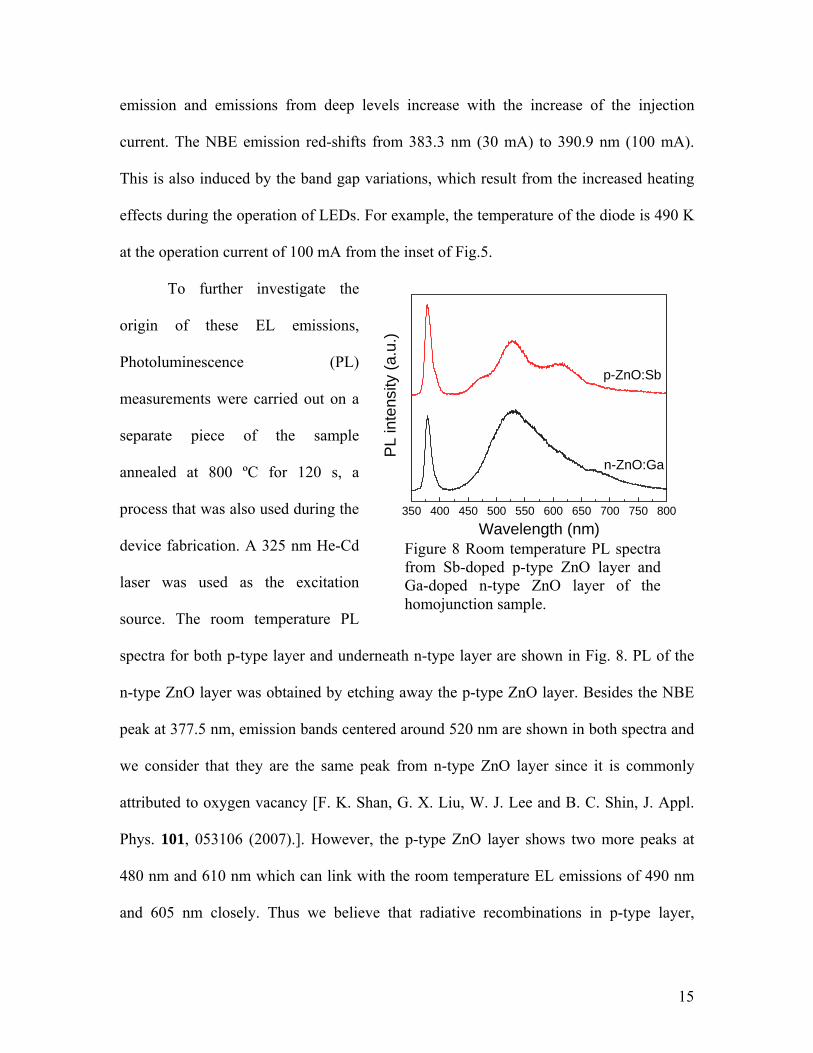
To further investigate the
origin of these EL emissions,
Photoluminescence (PL)
measurements were carried out on a
separate piece of the sample
annealed at 800 ºC for 120 s, a
process that was also used during the
device fabrication. A 325 nm He-Cd
laser was used as the excitation
source. The room temperature PL
spectra for both p-type layer and underneath n-type layer are shown in Fig. 8. PL of the
n-type ZnO layer was obtained by etching away the p-type ZnO layer. Besides the NBE
peak at 377.5 nm, emission bands centered around 520 nm are shown in both spectra and
we consider that they are the same peak from n-type ZnO layer since it is commonly
attributed to oxygen vacancy [F. K. Shan, G. X. Liu, W. J. Lee and B. C. Shin, J. Appl.
Phys. 101, 053106 (2007).]. However, the p-type ZnO layer shows two more peaks at
480 nm and 610 nm which can link with the room temperature EL emissions of 490 nm
and 605 nm closely. Thus we believe that radiative recombinations in p-type layer,
ity (a
.u.)
350 400 450 500 550 600 650 700 750 800
p-ZnO:Sb
PL
inte
ns
Wavelength (nm)
n-ZnO:Ga
Figure 8 Room temperature PL spectra from Sb-doped p-type ZnO layer and Ga-doped n-type ZnO layer of the homojunction sample.
15

including NBE transitions, have contributed mainly to the observed EL spectra. Similar
results were also observed in As-doped ZnO diode on GaAs substrate [J. C. Sun, J. Z.
Zhao, H. W. Liang, J. M. Bian, L. Z. Hu, H. Q. Zhang, X. P. Liang, W. F. Liu, G. T. Du,
Appl. Phys. Lett. 90, 121128 (2007)]. This is reasonable due to the fact that the
concentration of holes in p-type ZnO layer is less than the electron concentration of n-
type ZnO layer. As a result, the depletion region mostly exists in the p-type layer, and the
electron injection from the n-type layer to p-type layer dominates the recombination
process.
In conclusion, ZnO homojunction LEDs with the Sb-doped p-type ZnO layer/Ga-
doped n-type ZnO layer structure were fabricated and studied. The LEDs with the low
resistivity Au/NiO contacts for p-type ZnO showed very good UV emissions at different
temperatures and injection currents. This study suggests that Sb-doped p-type ZnO is
promising for future ZnO optoelectronics.
16