TEA5777 Low-power AM/FM stereo radio for handheld … · In FM mode the radio is completely...
48
IMPORTANT NOTICE Dear customer, As from August 2 nd 2008, the wireless operations of NXP have moved to a new company, ST-NXP Wireless. As a result, the following changes are applicable to the attached document. ● Company name - Philips Semiconductors is replaced with ST-NXP Wireless. ● Copyright - the copyright notice at the bottom of each page “© Koninklijke Philips Electronics N.V. 200x. All rights reserved”, shall now read: “© ST-NXP Wireless 200x - All rights reserved”. ● Web site - http://www.semiconductors.philips.com is replaced with http://www.stnwireless.com ● Contact information - the list of sales offices previously obtained by sending an email to [email protected] , is now found at http://www.stnwireless.com under Contacts. If you have any questions related to the document, please contact our nearest sales office. Thank you for your cooperation and understanding. ST-NXP Wireless www.stnwireless.com
Transcript of TEA5777 Low-power AM/FM stereo radio for handheld … · In FM mode the radio is completely...

IMPORTANT NOTICE
Dear customer,
As from August 2nd 2008, the wireless operations of NXP have moved to a new company,ST-NXP Wireless.
As a result, the following changes are applicable to the attached document.
Company name - Philips Semiconductors is replaced with ST-NXP Wireless.
Copyright - the copyright notice at the bottom of each page “© Koninklijke Philips Electronics N.V. 200x. All rights reserved”, shall now read: “© ST-NXP Wireless 200x - All rights reserved”.
Web site - http://www.semiconductors.philips.com is replaced with http://www.stnwireless.com
Contact information - the list of sales offices previously obtained by sending an email to [email protected], is now found at http://www.stnwireless.com under Contacts.
If you have any questions related to the document, please contact our nearest sales office.Thank you for your cooperation and understanding.
ST-NXP Wireless
www.stnwireless.com

1. General description
The TEA5777 is a BiCMOS single-chip (32-pin or 48-pin package), electronically tunedAM/FM stereo radio circuit, with fully integrated IF selectivity and demodulation includinglocal synthesized oscillator, and is intended to be used in electronically tuned radio sets.
In FM mode the radio is completely alignment free and in AM mode only a minimum ofantenna input alignment is required. The radio requires a minimum number of small andlow cost external components.
The IC communicates with a microcontroller via the I2C-bus or the 3-wire bus.
2. Features
2.1 Generaln High integration level of the AM and FM receiver means a very limited number of
external components are required
n On-board PLL synthesizer tuning function which includes VCOs, dividers, phasedetectors and charge pump
n FM mixer conversion for US and Europe, OIRT and Japanese band to IF
n Crystal reference frequency oscillator operating at 4 MHz
n External reference input frequency of 13 MHz (bus selectable)
n Autonomous search function
n IF counter with 1-bit output via the bus
n Silent readout of mono or stereo information and IF in-window indication
n Level detector with 4-bit level information output via the bus
n I2C-bus or 3-wire bus
n Standby mode switched via the bus
n 2 software programmable I/O ports with multiple functions
n Supply voltage range: 2.7 V to 7 V (typical 3 V)
n Low current consumption: 9.8 mA in AM mode and 13.9 mA in FM mode
2.2 AMn Fully integrated AM RF tuning function (no external varicap required)
n High-impedance MOSFET input
n Fully integrated AM IF filters
n Fully integrated AM VCO
n Integrated image rejection mixer structure
n LW and MW reception possibility
TEA5777Low-power AM/FM stereo radio for handheld applicationsRev. 01 — 11 April 2006 Product data sheet
Philips Semiconductors TEA5777Low-power AM/FM stereo radio for handheld applications
2.3 FMn High input sensitivity
n Fully integrated FM IF selectivity
n Fully integrated FM demodulator (no external discriminator)
n Integrated image rejection mixer structure
n RF LC oscillator operating with low cost fixed inductors (referenced to ground)
n FM I/Q mixer for conversion of the US, Europe, Japanese and OIRT band to IF
n Fully integrated, adjustment free, stereo decoder
n Signal dependent mono or stereo blend (with on and off function)
n FM stereo readout via the bus and silent readout mode
n RDS MPX output available
n Stereo decoder can be switched off via the bus
n Integrated anti-birdy filter
3. Applications
n Portable AM/FM stereo radio
n Mini and midi receiver sets
n PC radio applications
n GSM handsets
4. Quick reference data
Table 1. Quick reference dataVCCA = VCCD = 3 V; Tamb = 25 °C; all AC values are given in RMS.See Figure 9 for details on the dummy inputs Vi1, Vi2 and Vi3.
Symbol Parameter Conditions Min Typ Max Unit
General
VCCA analog supply voltage 2.7 3.0 7.0 V
VCCD digital supply voltage 2.7 3.0 5.0 V
ICCA analog supply current FM mode 10 13.9 17 mA
AM mode 8 9.8 11 mA
Standby modevia bus control
- 0.03 0.15 mA
ICCD digital supply current FM mode 0.5 0.8 1.5 mA
AM mode 0.5 0.8 1.5 mA
Standby modevia bus control
- 0.13 0.25 mA
Tamb ambient temperature −10 - +65 °C
Tuning
VO output voltage tuning voltage rangeon pin CPOUT
0.2 - VCCA −0.3
V
TEA5777_1 © Koninklijke Philips Electronics N.V. 2006. All rights reserved.
Product data sheet Rev. 01 — 11 April 2006 2 of 47

Philips Semiconductors TEA5777Low-power AM/FM stereo radio for handheld applications
[1] Programmable frequency range of the synthesizer referred to the antenna input.
[2] fRF = 100 MHz; ∆fFM(max) = 22.5 kHz; fmod = 1 kHz; τdeemp = 50 µs.
[3] The sensitivity at the dummy input is equivalent to EMF in a 75 Ω system.
Conditions: (S+N)/N = 26 dB; L = R; Baud(−3dB) = 300 Hz to 15 kHz, A-weighted; fIF = 133.333 kHz.
[4] Vi2 = 1 mV; ∆fFM(max) = 22.5 kHz.
[5] Vi2 = 1 mV; L = R; Baud(−3dB) = 300 Hz to 15 kHz, A-weighted; fIF = 133.333 kHz.
[6] Vi2 = 1 mV; ∆f = 75 kHz; with external τdeemp = 50 µs; Baud(−3dB) limited to 15 kHz.
[7] fRF = 918 kHz; m = 0.3; fmod = 1 kHz; τdeemp = 75 µs
fRF RF frequency FM [1]
fstep = 10 kHz;fIF = 150 kHz
10.24 - 81.91 MHz
fstep = 33.333 kHz;fIF = 133.333 kHz
34.13 - 273.03 MHz
fstep = 50 kHz;fIF = 150 kHz
51.2 - 409.55 MHz
AM; fstep = 1 kHz;fIF = 21 kHz
[1]
LW 128 - 511.75 kHz
MW 512 - 2047 kHz
FM performance [2]
Vi input voltage Vi = Vi2 =RF sensitivity atdummy input
[3] - 2.7 3.5 µV
Vo(AF) AF output voltage measured on pinsVAFL and VAFR
[4]
fIF = 133.333 kHz 70 95 120 mV
fIF = 150 kHz 55 75 95 mV
S/N signal-to-noise ratio measured on pinMPXOUT
- 60 - dB
THD total harmonic distortion measured on pinMPXOUT
[6] - 0.55 1.5 %
AM performance [7]
Vi input voltage Vi = Vi1 =RF sensitivity atdummy input
[8] - 155 - µV
E electric field strength RF sensitivity withferroceptor
[9] - 2.9 - mV/m
Vo(AF) AF output voltage measured on pinsVAFL and VAFR
[10] 72 90 108 mV
S/N signal-to-noise ratio [11] 40 48 - dB
THD total harmonic distortion [12] - 1 2.5 %
MPX stereo decoder performance
αcs channel separation [13] 26 40 - dB
Table 1. Quick reference data …continuedVCCA = VCCD = 3 V; Tamb = 25 °C; all AC values are given in RMS.See Figure 9 for details on the dummy inputs Vi1, Vi2 and Vi3.
Symbol Parameter Conditions Min Typ Max Unit
TEA5777_1 © Koninklijke Philips Electronics N.V. 2006. All rights reserved.
Product data sheet Rev. 01 — 11 April 2006 3 of 47
Philips Semiconductors TEA5777Low-power AM/FM stereo radio for handheld applications
[8] Conditions: (S+N)/N = 26 dB; m = 0.3; A-weighting filter.
[9] With ferroceptor C8E-A0424 TOKO Inc; (S+N)/N = 26 dB; A-weighting filter.
[10] Vi1 = 5 mV.
[11] Vi1 = 5 mV; A-weighting filter.
[12] Vi1 = 5 mV; m = 0.8; bit AGCRF = 0 (slow AGC RF); bit AGCIF = 0 (slow AGC IF); Baud(−3dB) limited to15 kHz.
[13] Vi3 = 300 mV; fmod = 1 kHz; Vpilot = 30 mV; R = 1 and L = 0 or R = 0 and L = 1; VTMUTE = 1 V;fIF = 133.333 kHz; Baud(−3dB) limited to 15 kHz.
5. Ordering information
Table 2. Ordering information
Type number Package
Name Description Version
TEA5777HN HVQFN48 plastic thermal enhanced very thin quad flatpackage; no leads; 48 terminals;body 7 × 7 × 0.85 mm
SOT619-1
TEA5777HL LQFP32 plastic low profile quad flat package; 32 leads;body 7 × 7 × 1.4 mm
SOT358-1
TEA5777_1 © Koninklijke Philips Electronics N.V. 2006. All rights reserved.
Product data sheet Rev. 01 — 11 April 2006 4 of 47
xxxx xxxxxxxxxxxxxxxxxxxxxxxxxxxxxx x xxxxxxxxxxxxxx xxxxxxxxxx xxx xxxxxx xxxxxxxxxxxxxxxxxxxxxxx xxxxxxxxxxxxxxxxxxxxxxxxxxx xxxxxx xx xxxxxxxxxxxxxxxxxxxxxxxxxxxxx xxxxxxxxxxxxxxxxxxxxxx xxxxxxxxxxx xxxxxxx xxxxxxxxxxxxxxxxxxxxxxxxxxxxxxxxxxx xxxxxxxxxxxxxx xxxxxx xx xxxxxxxxxxxxxxxxxxxxxxxxxxxxxxxx xxxxxxxxxxxxxxxxxxxxxxxx xxxxxxxxxxxxxxxxxxxxxxxxxxxxxxxxxxxxxxxxxxxxxxxxxxxxx xxxxxxxxxxx xxxxx x x
TE
A5777_1
Product data shee
Philips S
emiconduc
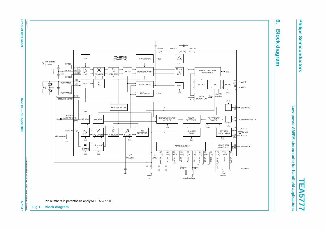
6.B
lock diagram
t
AGC
MPXINTMUTE MPXOUT
22 (15) 36 (24) 33 (22)
TEA5777HNIF COUNTER bus
torsTE
A5777
Low-pow
er AM
/FM
stereo radio for handheld applications
001aab435
BUSMODE
SWPORT2/EXTIN
SWPORT1
VAFL
VAFR
XTAL2
XTAL1
4 MHz
buscontrol
WR
ITE
_RE
AD
DA
TA
CLO
CK
20(14)
19(13)
18(12)
38(25)
14(9)
16(11)
10(7)
9(6)
31(21)
34(23)
R
NCEER
I2C-BUS AND3-WIRE BUS
CRYSTALOSCILLATOR
MUTEUX
bus
bus
bus
bus
AM/FMselection
bus
© K
oninklijke Philips E
lectronics N.V. 2006. A
ll rights reserved.
Rev. 01 —
11 April 2006
5 of 47
Pin numbers in parenthesis apply to TEA5777HL.
Fig 1. Block diagram
RF AGC
VCO÷2N1
VCOTANK1
GNDVCO_AMRF
PILDET/AMRFAGC
AMRFIN
AGC2CAP CPOUT
supply voltage
GN
DA
GN
DIF
VC
CD
VC
CA
V25
DIG
V25
IF
VA
MLN
A
VR
EF
VCOTANK2
RFIN2
GNDRF
RFIN1
43 (28)44 (29)
45 (30)
4 (3)
3 (2)
5 (4)
46(31)
7 (5)
27 (18) 2 (1)47(32)
40(26)
30(20)
26(17)
23(16)
11(8)
41(27)
29(19)
GN
DD
15(10)
FM antenna
AM antenna
AM VCO
C-BANK
÷ 8 or ÷ 32N1
LNA I/Q MIXER IF FILTER LPF
80 kHz
SDS
LIMITER
SLOW LEVEL
MASTER FILTER
(TEA5777HL)
ADC (4-bit)
PROGRAMMABLEDIVIDER
PHASEDETECTOR
PILOTDETECTOR
STEREO DECODEREFERENCE
REFEREDIVID
CHARGEPUMP
POWER SUPPLY
MMATRIX
DEMODULATOR
I/Q MIXER IF FILTER IF AGC
AMDETECTOR
bus
busbusbus
bus
bus
bus bus
busbus
bus

Philips Semiconductors TEA5777Low-power AM/FM stereo radio for handheld applications
7. Pinning information
7.1 Pinning
Fig 2. Pin configuration HVQFN48
001aab434
TEA5777HN
n.c.
VCCD
n.c.
VREF
SWPORT2/EXTIN AGC2CAP
SWPORT1 n.c.
n.c. GNDA
AMRFIN V25DIG
n.c. VAFL
GNDVCO_AMRF n.c.
VCOTANK2 MPXIN
VCOTANK1 VAFR
CPOUT n.c.
n.c. MPXOUT
n.c.
XT
AL2
GN
DD
XT
AL1 n.c.
CLO
CK
DA
TA
WR
ITE
_RE
AD
n.c.
TM
UT
E
VC
CA
n.c.
n.c.
VA
MLN
A
PIL
DE
T/A
MR
FA
GC
RF
IN2
GN
DR
F
RF
IN1
n.c.
GN
DIF
V25
IF
n.c.
BU
SM
OD
E
n.c.
12 25
11 26
10 27
9 28
8 29
7 30
6 31
5 32
4 33
3 34
2 35
1 36
13 14 15 16 17 18 19 20 21 22 23 24
48 47 46 45 44 43 42 41 40 39 38 37
terminal 1index area
Transparent top view
TEA5777_1 © Koninklijke Philips Electronics N.V. 2006. All rights reserved.
Product data sheet Rev. 01 — 11 April 2006 6 of 47
Philips Semiconductors TEA5777Low-power AM/FM stereo radio for handheld applications
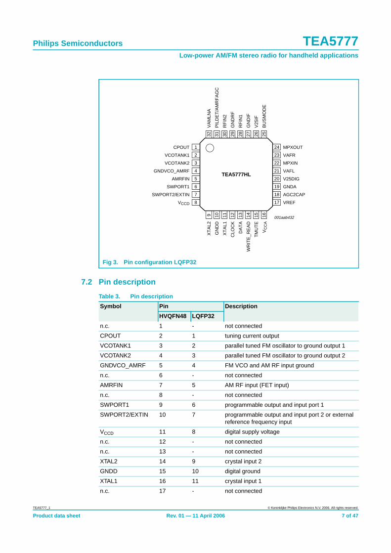
7.2 Pin description
Fig 3. Pin configuration LQFP32
TEA5777HL
CPOUT MPXOUT
VCOTANK1 VAFR
VCOTANK2 MPXIN
GNDVCO_AMRF VAFL
AMRFIN V25DIG
SWPORT1 GNDA
SWPORT2/EXTIN AGC2CAP
VCCD VREFX
TA
L2V
AM
LNA
GN
DD
PIL
DE
T/A
MR
FA
GC
XT
AL1
RF
IN2
CLO
CK
GN
DR
F
DA
TA
RF
IN1
WR
ITE
_RE
AD
GN
DIF
TM
UT
EV
25IF
VC
CA
BU
SM
OD
E
001aab432
1
2
3
4
5
6
7
8
24
23
22
21
20
19
18
179 10 11 12 13 14 15 16
32 31 30 29 28 27 26 25
Table 3. Pin description
Symbol Pin Description
HVQFN48 LQFP32
n.c. 1 - not connected
CPOUT 2 1 tuning current output
VCOTANK1 3 2 parallel tuned FM oscillator to ground output 1
VCOTANK2 4 3 parallel tuned FM oscillator to ground output 2
GNDVCO_AMRF 5 4 FM VCO and AM RF input ground
n.c. 6 - not connected
AMRFIN 7 5 AM RF input (FET input)
n.c. 8 - not connected
SWPORT1 9 6 programmable output and input port 1
SWPORT2/EXTIN 10 7 programmable output and input port 2 or externalreference frequency input
VCCD 11 8 digital supply voltage
n.c. 12 - not connected
n.c. 13 - not connected
XTAL2 14 9 crystal input 2
GNDD 15 10 digital ground
XTAL1 16 11 crystal input 1
n.c. 17 - not connected
TEA5777_1 © Koninklijke Philips Electronics N.V. 2006. All rights reserved.
Product data sheet Rev. 01 — 11 April 2006 7 of 47

Philips Semiconductors TEA5777Low-power AM/FM stereo radio for handheld applications
CLOCK 18 12 I2C-bus and 3-wire bus clock input
DATA 19 13 I2C-bus and 3-wire bus data input and output
WRITE_READ 20 14 3-wire bus write and read input
n.c. 21 - not connected
TMUTE 22 15 field strength indicator capacitor connection
VCCA 23 16 analog supply voltage
n.c. 24 - not connected
n.c. 25 - not connected
VREF 26 17 1.25 V stabilized reference voltage output
AGC2CAP 27 18 AM IF AGC capacitor connection
n.c. 28 - not connected
GNDA 29 19 analog ground
V25DIG 30 20 internal stabilized supply voltage (digital part)output
VAFL 31 21 left channel output
n.c. 32 - not connected
MPXIN 33 22 stereo decoder input
VAFR 34 23 right channel output
n.c. 35 - not connected
MPXOUT 36 24 FM MPX output
n.c. 37 - not connected
BUSMODE 38 25 bus mode selection input
n.c. 39 - not connected
V25IF 40 26 internal stabilized supply voltage (IF, demodulatorand integrated birdy filter) output
GNDIF 41 27 ground of IF, demodulator and integrated birdyfilter
n.c. 42 - not connected
RFIN1 43 28 FM RF antenna input 1
GNDRF 44 29 FM RF ground
RFIN2 45 30 FM RF antenna input 2
PILDET/AMRFAGC 46 31 stereo decoder pilot detector filter input or AM RFAGC capacitor connection
VAMLNA 47 32 internal stabilized supply voltage (AM front end)output
n.c. 48 - not connected
Table 3. Pin description …continued
Symbol Pin Description
HVQFN48 LQFP32
TEA5777_1 © Koninklijke Philips Electronics N.V. 2006. All rights reserved.
Product data sheet Rev. 01 — 11 April 2006 8 of 47
Philips Semiconductors TEA5777Low-power AM/FM stereo radio for handheld applications
8. Functional description
The TEA5777 is an integrated AM/FM stereo radio circuit with very high integration levelincluding digital tuning and control functions.
The IC communicates with a microcontroller via the I2C-bus or the 3-wire bus interfaceand provides the following functions:
• AM single conversion receiver with integrated image rejection for fIF = 21 kHz
• FM single conversion receiver with integrated image rejection for fIF = 133.333 kHz or150 kHz (software selectable)
• FM stereo decoder with signal dependent stereo effect
The AM circuit incorporates:
• Integrated antenna tuning function
• Integrated I/Q IF channel
• On-chip image reject mixer structure
• A fully integrated AM VCO with fVCO = 8 × (fRF + fIF)
• Software selectable high-side or low-side oscillator injection
• A fully integrated AM detector
The FM circuit incorporates:
• Integrated I/Q IF channel
• On-chip image reject mixer structure
• External RF VCO running at fVCO = 2 × (fRF ± fIF)
• Software selectable high-side or low-side oscillator injection
• A fully integrated demodulator
• Japan band possibility
The stereo decoder incorporates:
• A 1.52 MHz VCO, that needs no external adjustment, which can lock to the 19 kHzstereo pilot tone by means of a PLL system; the sub-carrier frequencies of 19 kHz,38 kHz and others are regenerated from the VCO output
• Integrated 50 µs or 75 µs (switchable) de-emphasis
• Signal Dependent Stereo (SDS) function can be switched off via the bus interface
• Stereo decoder can be switched off in order to save power
Tuning function:
• The tuning synthesizer is on-chip with the radio and utilizes a PLL system for tuningand an IF counter has been added for search-stop detection
• Tuning to a wanted input signal can be achieved by preset tuning or search tuning. Forthe latter the IC has a built-in auto search function which reduces the load of themicrocontroller
TEA5777_1 © Koninklijke Philips Electronics N.V. 2006. All rights reserved.
Product data sheet Rev. 01 — 11 April 2006 9 of 47
Philips Semiconductors TEA5777Low-power AM/FM stereo radio for handheld applications
Bus communication:
• Bus communication takes place via the I2C-bus or the 3-wire bus protocol. Selectionof the bus mode is done by hardware programming via pin BUSMODE
• 4-bit ADC level information, 1-bit IF counter and mono or stereo indication (in FMmode) can be read via the bus. Alternatively, the mono or stereo and the IF in-windowindication can be obtained via silent readout via the bus lines CLOCK and DATA
8.1 AM radio part
8.1.1 AM RF amplifier
The AM input pin AMRFIN has a (selectable) high-impedance input. The input is intendedto be connected to the top of a tuned circuit. The input impedance is determined by theLNA gain (bit LNA) and the value of the LNA feedback resistor (bit RFB).
For large RF input signals, the RF AGC reduces the input signal level to the AM front endin order to prevent overloading. The required AM RF AGC time constant is created bymeans of an internal current source and the capacitor connected to pinPILDET/AMRFAGC. During search operation the response time of this RF AGC circuitcan be speeded up via the bus control by bit AGCRF.
8.1.2 Tuning AM antenna circuit
The tuning capacitor for the AM antenna circuit has been integrated by means of acapacitor bank (C-bank) and the tuning frequency can be programmed in discrete stepsvia the bus. No external varactor diode is required. In order to match the capacitor bank tothe external AM antenna coil, a provision has been made to electronically align the IC tothe AM antenna. For this bit CALLIGN has to be set to logic 1 and the corresponding bitsC[6:0] have to be programmed. After this alignment bit CALLIGN should be set to logic 0again to freeze the alignment capacitor value and to enable the control over the maincapacitor bank again.
For more details on the alignment, see Section 13.1 and the application note.
For LW mode an external capacitor needs to be added in parallel to the LW coil.
8.1.3 AM I/Q mixer
AM quadrature mixers, in an orthogonal architecture, convert AM RF signals to theinternal fIF = 21 kHz. The mixer architecture provides inherent image rejection.
8.1.4 AM VCO
The fully integrated VCO provides the local oscillator signals for the AM quadraturemixers. No external components are required.
The internal VCO frequency ranges from 4 MHz to 14 MHz and the proper divider ratio ischosen by selecting the MW or LW band via the bus control bit MWLW.
Programming of the VCO is done:
• For MW: fVCO = 8 × (fRF ± fIF)
• For LW: fVCO = 32 × (fRF ± fIF)
TEA5777_1 © Koninklijke Philips Electronics N.V. 2006. All rights reserved.
Product data sheet Rev. 01 — 11 April 2006 10 of 47

Philips Semiconductors TEA5777Low-power AM/FM stereo radio for handheld applications
High-side injection or low-side injection of the VCO can be chosen:
• High-side injection: local oscillator frequency at mixer input is higher than RF inputsignal frequency.
• Low-side injection: local oscillator frequency at mixer input is lower than RF inputsignal frequency.
8.1.5 AM IF filter
The AM circuit incorporates an I and Q orthogonal channel path with fully integratedpolyphase IF filter. All AM IF filtering is done inside the IC, therefore no external filtercomponents are required. The center frequency of the filter is 21 kHz and the −3 dBbandwidth amounts to 8 kHz.
8.1.6 AM IF amplification and AM detection
The IF AGC controls the IF amplification and a fully integrated AM detector converts theAM IF signal into audio. In AM mode the capacitor connected to pin AGC2CAP is used forIF AGC filtering. The value of this capacitor is a compromise between AGC speed andTHD. In order to achieve an acceptable THD in normal mode and an acceptable AGCresponse during e.g. a search action, the time constant can be switched to a value15 times lower by means of bit AGCIF. In autonomous search mode (bit SEARCH = 1) thetime constant is switched automatically to the lowest value.
8.2 FM radio part
8.2.1 Low noise RF amplifier
The FM circuit incorporates a wideband input. The LNA input impedance together with theLC RF input circuit defines a low Q, FM band-pass filter. The input filter is also used forimpedance matching between the source impedance and the 300 Ω LNA inputimpedance between pins RFIN1 and RFIN2. An RF AGC circuit prevents the mixer and IFfilter from overdrive conditions.
8.2.2 FM I/Q mixer
FM quadrature mixers, in an orthogonal I/Q architecture, convert FM RF signals to theinternal fIF = 133.333 kHz or 150 kHz. The mixer architecture provides inherent imagerejection. Whether fIF = 133.333 kHz or 150 kHz is chosen depends on bits FREF[1:0].
For choosing the best signal conditions with respect to the influence of the image signals,high-side or low-side injection can be selected:
• High-side injection: local oscillator frequency at mixer input is higher than RF inputsignal frequency.
• Low-side injection: local oscillator frequency at mixer input is lower than RF inputsignal frequency.
TEA5777_1 © Koninklijke Philips Electronics N.V. 2006. All rights reserved.
Product data sheet Rev. 01 — 11 April 2006 11 of 47

Philips Semiconductors TEA5777Low-power AM/FM stereo radio for handheld applications
8.2.3 FM VCO
The symmetrical LC, varactor tuned VCO provides the oscillator signals for the FMquadrature mixers (pins VCOTANK1 and VCOTANK2). The VCO operates at double theRF frequency fVCO = 2 × (fRF ± fIF) and has an internal AGC control circuit in order toguarantee good start-up behavior and carrier-to-noise ratio (C/N) even with low Q coils(Q > 40). High-side injection (+fIF) or low-side injection (−fIF) of the VCO can be chosenvia the bus control.
8.2.4 FM IF filter
The FM signal path incorporates an I and Q orthogonal FM channel with fully integratedpolyphase IF filter. All FM IF filtering is done inside the IC, therefore no external filtercomponents are required. The center frequency of the filter matches the chosen IF(fIF = 133.333 kHz or 150 kHz) and has a −3 dB bandwidth of approximately 110 kHz.
8.2.5 FM demodulator
The FM demodulator is fully integrated and needs no external components. In order toremove undesired IF and or RF input related components, a 80 kHz low-pass filter hasbeen integrated.
8.3 Stereo decoder
8.3.1 MPX decoder
The PLL stereo decoder is alignment free and incorporates a fully integrated PLL loopfilter. The stereo decoder can be switched to forced mono via bus control bit FOMO.
8.3.2 Signal strength depending mono/stereo blend
When decreasing the RF input level, the MPX decoder blends from stereo to mono to limitthe output noise. The control signal is obtained from the low-pass filtered level informationat pin TMUTE. This blend function, called SDS, can also be switched off via bus control bitSDSOFF and a RF level related sudden change from stereo to mono transition will result.
8.3.3 Pilot detector
A pilot detector, with external filter capacitor at pin PILDET/AMRFAGC, is used to detectthe presence of a stereo signal. Mono or stereo reception can be read via the bus control,but can also be passed to pin DATA in the Dbus mode (see Section 9). For this option, bitDBUS has to be programmed. In this case, no bus action is required (silent readout) toread the status of the pilot detector and the information is continuously available.
8.3.4 De-emphasis
In FM mode, the de-emphasis is switchable between 50 µs and 75 µs (bit DEEM). In AMmode, bit DEEM selects a low-pass filter with the time constant 50 µs or 75 µs in order tolimit the noise bandwidth.
8.4 Tuning functionThe tuning concept of the TEA5777 is based on a PLL and programming of the requiredfrequency takes place via the bus control.
TEA5777_1 © Koninklijke Philips Electronics N.V. 2006. All rights reserved.
Product data sheet Rev. 01 — 11 April 2006 12 of 47

Philips Semiconductors TEA5777Low-power AM/FM stereo radio for handheld applications
8.4.1 Reference frequency generation
The internally required reference frequency can be obtained from the integrated crystaloscillator or from an externally applied reference signal of 13 MHz. Selection of thereference signal (internal or external) takes place via the bus control.
The reference frequency signals are used for:
• Reference frequency divider for the PLL synthesizer
• Center frequency adjustment of the IF filters
• Free running frequency adjustment of the stereo decoder VCO
• Clocking the stereo decoder state machine
• Timing of the IF counter
• Sampling the RF level for the level ADC
8.4.2 Crystal oscillator
The symmetrical crystal oscillator can operate with a 4 MHz clock crystal. An amplitudecontrol function is implemented in order to minimize the higher harmonic componentsignal levels.
8.4.3 IF counter
An IF counter has been added for search-stop detection (optional, i.e. can be enabled ordisabled via bit IFCE). The IF counter result is a 1-bit output and in-window yes or no andavailable via bus control. In order to minimize the interference, the IF counter can bedisabled via the bus control bit IFCE. In both AM and FM modes, two IF window settingscan be chosen by bit IFW.
When Dbus mode is activated and bit IFCE = 1, the IF counter result is available at pinDATA (see Table 8). In this mode, the IF counter ready flag (bit IFCRDY) is put on pinDATA. Disabling bit IFCE, while Dbus mode is active, puts the mono or stereo indicationinformation on pin DATA. In this case no bus actions are required to read the status of theIF counter (silent readout).
Remark: For updating the IF counter information a short pulse on pin WRITE_READshould be generated.
8.4.4 Automatic search operation
The IC can be programmed to an autonomous search mode operation. In this mode, theIC will search for a new station without the need of communication to the microcontroller.To enable this mode, bit SEARCH has to be set. Under control of bit UPDWN, search stoplevel bits SLEV[1:0] and search step control bits STEP[1:0], various search modes can beselected (see Section 9).
Before this mode can be activated, first the upper and lower band limits have to beprogrammed. Bit PROGBLIM = 1 and bit UPDWN = 1 programs the upper band limit,while bit PROGBLIM = 1 and bit UPDWN = 0 programs the lower band limit. Bit SFOUNDsignals whether a new station is found. Bit BLIM signals whether a band limit is reached.
In AM mode, bit AMDELAY selects either a 40 ms or 80 ms delay time. The best value tobe selected depends on the realized AM IF AGC response (see Section 8.1.6).
TEA5777_1 © Koninklijke Philips Electronics N.V. 2006. All rights reserved.
Product data sheet Rev. 01 — 11 April 2006 13 of 47

Philips Semiconductors TEA5777Low-power AM/FM stereo radio for handheld applications
8.5 RF level information (RSSI)For processing Receiver Signal Strength Information (RSSI) in both AM and FM modes,the internal level voltage is analog-to-digital converted with a 4-bit ADC. The levelinformation can be read by bits LEV[3:0] in the read register. In autonomous search mode,bits LEV[3:0] still indicate some momentary level information, however the data isdependent upon the readout timing and can be considered to have no relevance to theuser. The ADC full-scale goes from 0.25 V to 0.95 V. In AM mode, the level informationcovers the ADC full-scale. In FM mode, the level information does not fully cover the ADCfull-scale.
8.6 Software programmable portsTwo software programmable ports can be addressed via the bus control. These ports canbe independently switched to multiple functions, knowing:
• Outputs: SWPORT1 and SWPORT2 can act as output ports which are capable ofsourcing and sinking approximately 9 mA.
• Inputs: SWPORT1 and SWPORT2 can act as input ports of which the status can beread out via bus control.
Remark: Port SWPORT2 can be switched as input for the 13 MHz reference signal. Inthat case, no other functions can be programmed for this port.
TEA5777_1 © Koninklijke Philips Electronics N.V. 2006. All rights reserved.
Product data sheet Rev. 01 — 11 April 2006 14 of 47
Philips Semiconductors TEA5777Low-power AM/FM stereo radio for handheld applications
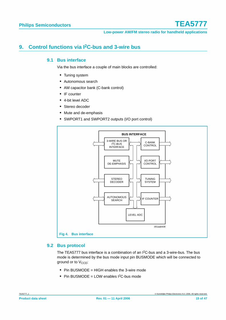
9. Control functions via I 2C-bus and 3-wire bus
9.1 Bus interfaceVia the bus interface a couple of main blocks are controlled:
• Tuning system
• Autonomous search
• AM capacitor bank (C-bank control)
• IF counter
• 4-bit level ADC
• Stereo decoder
• Mute and de-emphasis
• SWPORT1 and SWPORT2 outputs (I/O port control)
9.2 Bus protocolThe TEA5777 bus interface is a combination of an I2C-bus and a 3-wire-bus. The busmode is determined by the bus mode input pin BUSMODE which will be connected toground or to VCCD:
• Pin BUSMODE = HIGH enables the 3-wire mode
• Pin BUSMODE = LOW enables I2C-bus mode
Fig 4. Bus interface
001aab436
3-WIRE BUS ORI2C-BUS
INTERFACE
MUTEDE-EMPHASIS
STEREODECODER
AUTONOMOUSSEARCH
C-BANKCONTROL
I/O PORTCONTROL
TUNINGSYSTEM
IF COUNTER
LEVEL ADC
BUS INTERFACE
TEA5777_1 © Koninklijke Philips Electronics N.V. 2006. All rights reserved.
Product data sheet Rev. 01 — 11 April 2006 15 of 47
Philips Semiconductors TEA5777Low-power AM/FM stereo radio for handheld applications
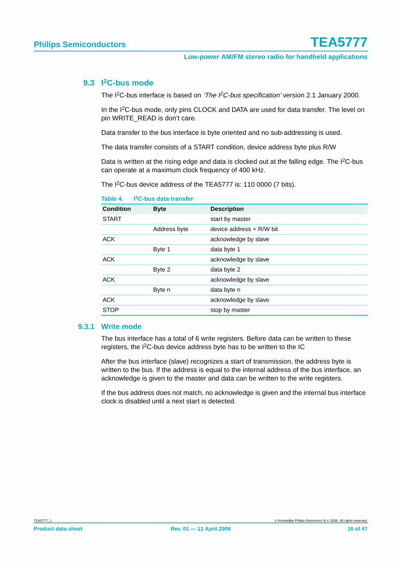
9.3 I2C-bus modeThe I2C-bus interface is based on ‘The I2C-bus specification’ version 2.1 January 2000.
In the I2C-bus mode, only pins CLOCK and DATA are used for data transfer. The level onpin WRITE_READ is don’t care.
Data transfer to the bus interface is byte oriented and no sub-addressing is used.
The data transfer consists of a START condition, device address byte plus R/W
Data is written at the rising edge and data is clocked out at the falling edge. The I2C-buscan operate at a maximum clock frequency of 400 kHz.
The I2C-bus device address of the TEA5777 is: 110 0000 (7 bits).
9.3.1 Write mode
The bus interface has a total of 6 write registers. Before data can be written to theseregisters, the I2C-bus device address byte has to be written to the IC
After the bus interface (slave) recognizes a start of transmission, the address byte iswritten to the bus. If the address is equal to the internal address of the bus interface, anacknowledge is given to the master and data can be written to the write registers.
If the bus address does not match, no acknowledge is given and the internal bus interfaceclock is disabled until a next start is detected.
Table 4. I2C-bus data transfer
Condition Byte Description
START start by master
Address byte device address + R/W bit
ACK acknowledge by slave
Byte 1 data byte 1
ACK acknowledge by slave
Byte 2 data byte 2
ACK acknowledge by slave
Byte n data byte n
ACK acknowledge by slave
STOP stop by master
TEA5777_1 © Koninklijke Philips Electronics N.V. 2006. All rights reserved.
Product data sheet Rev. 01 — 11 April 2006 16 of 47

Philips Semiconductors TEA5777Low-power AM/FM stereo radio for handheld applications
9.3.2 Read mode
The bus interface has a total of 3 read bytes. If a start of transmission is detected and theI2C-bus device address matches with the internal address, an acknowledge is given andthe data is clocked out. If not, the internal clock is disabled and the data output will belogic 1s (FFh).
9.3.3 Dbus function in I 2C-bus mode (silent readout)
The Dbus function becomes active when bit DBUS = 1 and when the maximum availablebytes are written in the write mode or when the maximum available bytes are read in theread mode. At every start of an I2C-bus data transfer, the Dbus mode is deactivated.
When the Dbus mode is active in I2C-bus mode, pin WRITE_READ becomes anopen-collector output (pull-up resistor required). Depending on the setting of bit IFCE andbit SEARCH, the following data will be available at pin WRITE_READ:
• Mono or stereo indication flag
• IFC counter flag
• SFOUND flag or BLIM reached flag
In Table 7 the data at pin WRITE_READ is depicted as a function of bits DBUS, SEARCHand IFCE.
Table 5. I2C-bus write mode
Condition Byte Description
START start by master
Address byte 1100 0000 (bit R/W = 0)
ACK acknowledge by slave
Byte 1 data byte 1
ACK acknowledge by slave
Byte 2 data byte 2
ACK acknowledge by slave
: :
Byte 6 data byte 6
ACK acknowledge by slave
STOP stop by master
Table 6. I2C-bus read mode
Condition Byte Description
START start by master
Address byte 1100 0001 (bit R/W = 1)
ACK acknowledge by slave
Byte 1 data byte 1
ACK acknowledge by slave
Byte 2 data byte 2
ACK acknowledge by slave
Byte 3 data byte 3
STOP stop by master
TEA5777_1 © Koninklijke Philips Electronics N.V. 2006. All rights reserved.
Product data sheet Rev. 01 — 11 April 2006 17 of 47
Philips Semiconductors TEA5777Low-power AM/FM stereo radio for handheld applications
[1] H = HIGH-level output voltage
L = LOW-level output voltage
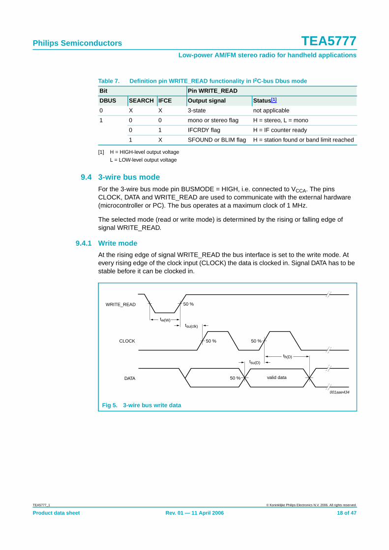
9.4 3-wire bus modeFor the 3-wire bus mode pin BUSMODE = HIGH, i.e. connected to VCCA. The pinsCLOCK, DATA and WRITE_READ are used to communicate with the external hardware(microcontroller or PC). The bus operates at a maximum clock of 1 MHz.
The selected mode (read or write mode) is determined by the rising or falling edge ofsignal WRITE_READ.
9.4.1 Write mode
At the rising edge of signal WRITE_READ the bus interface is set to the write mode. Atevery rising edge of the clock input (CLOCK) the data is clocked in. Signal DATA has to bestable before it can be clocked in.
Table 7. Definition pin WRITE_READ functionality in I 2C-bus Dbus mode
Bit Pin WRITE_READ
DBUS SEARCH IFCE Output signal Status [1]
0 X X 3-state not applicable
1 0 0 mono or stereo flag H = stereo, L = mono
0 1 IFCRDY flag H = IF counter ready
1 X SFOUND or BLIM flag H = station found or band limit reached
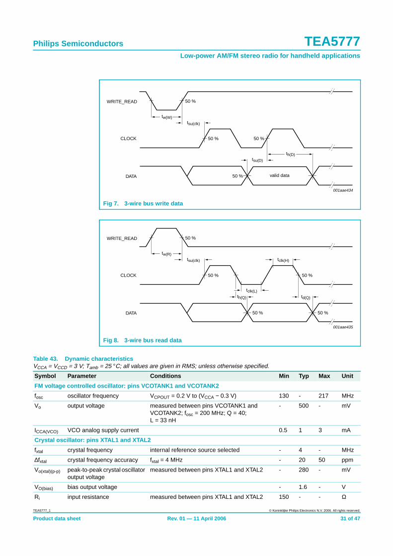
Fig 5. 3-wire bus write data
001aae434
50 %
tsu(clk)
tsu(D)
valid data
tw(W)
50 % 50 %
50 %WRITE_READ
CLOCK
DATA
th(D)
TEA5777_1 © Koninklijke Philips Electronics N.V. 2006. All rights reserved.
Product data sheet Rev. 01 — 11 April 2006 18 of 47
Philips Semiconductors TEA5777Low-power AM/FM stereo radio for handheld applications
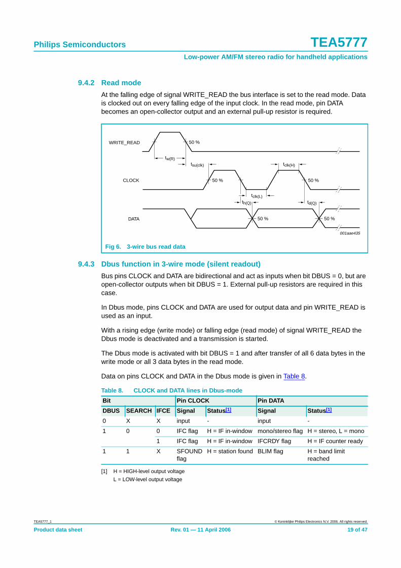
9.4.2 Read mode
At the falling edge of signal WRITE_READ the bus interface is set to the read mode. Datais clocked out on every falling edge of the input clock. In the read mode, pin DATAbecomes an open-collector output and an external pull-up resistor is required.
9.4.3 Dbus function in 3-wire mode (silent readout)
Bus pins CLOCK and DATA are bidirectional and act as inputs when bit DBUS = 0, but areopen-collector outputs when bit DBUS = 1. External pull-up resistors are required in thiscase.
In Dbus mode, pins CLOCK and DATA are used for output data and pin WRITE_READ isused as an input.
With a rising edge (write mode) or falling edge (read mode) of signal WRITE_READ theDbus mode is deactivated and a transmission is started.
The Dbus mode is activated with bit DBUS = 1 and after transfer of all 6 data bytes in thewrite mode or all 3 data bytes in the read mode.
Data on pins CLOCK and DATA in the Dbus mode is given in Table 8.
[1] H = HIGH-level output voltage
L = LOW-level output voltage
Fig 6. 3-wire bus read data
001aae435
50 % 50 %
tsu(clk) tclk(H)
tclk(L)td(Q)th(Q)
tw(R)
50 % 50 %
50 %WRITE_READ
CLOCK
DATA
Table 8. CLOCK and DATA lines in Dbus-mode
Bit Pin CLOCK Pin DATA
DBUS SEARCH IFCE Signal Status [1] Signal Status [1]
0 X X input - input -
1 0 0 IFC flag H = IF in-window mono/stereo flag H = stereo, L = mono
1 IFC flag H = IF in-window IFCRDY flag H = IF counter ready
1 1 X SFOUNDflag
H = station found BLIM flag H = band limitreached
TEA5777_1 © Koninklijke Philips Electronics N.V. 2006. All rights reserved.
Product data sheet Rev. 01 — 11 April 2006 19 of 47
Philips Semiconductors TEA5777Low-power AM/FM stereo radio for handheld applications
9.5 Data transfer in I 2C-bus and 3-wire modeIn the write mode, the data transfer between the TEA5777 (slave) and the microcontroller(master) is byte oriented.
In the read mode, the data transfer from slave to master is bit oriented.
Remark: For writing to the PLL, it is necessary to write both the first and second databyte. Only after completing the data transfer of data byte 2 is the PLL word copied into thePLL register.
9.5.1 Register definition in write mode
9.5.1.1 FM write mode
Table 9. Survey of bit names in FM write modeBits marked with * are common for FM and AM mode.
Bits 7 6 5 4 3 2 1 0
Byte 1 MUTE* AM/FM* STB* PLL12 PLL11 PLL10 PLL9 PLL8
Byte 2 PLL7 PLL6 PLL5 PLL4 PLL3 PLL2 PLL1 PLL0
Byte 3 FREF1 FREF0 IFCE* IFW* HILO* DBUS* - INTEXT*
Byte 4 P1* P0* PEN1* PEN0* - CHP0* DEEM* -
Byte 5 FOMO SDSOFF DOFF - - - - -
Byte 6 SEARCH* PROGBLIM* UPDWN* SLEV1* SLEV0* STEP1 STEP0* -
Table 10. FM write mode - data byte 1Bits marked with * are common for FM and AM mode.
Bit Symbol Description
7 (MSB) MUTE* audio mute: 0 = audio not muted; 1 = audio muted
6 AM/FM* AM/FM selection: 0 = FM; 1 = AM
5 STBY* operating mode: 0 = operating; 1 = standby
4 PLL12 setting of synthesizer programmable counter
3 PLL11
2 PLL10
1 PLL9
0 (LSB) PLL8
Table 11. FM write mode - data byte 2Bits marked with * are common for FM and AM mode.
Bit Symbol Description
7 (MSB) PLL7 setting of synthesizer programmable counter
6 PLL6
5 PLL5
4 PLL4
3 PLL3
2 PLL2
1 PLL1
0 (LSB) PLL0
TEA5777_1 © Koninklijke Philips Electronics N.V. 2006. All rights reserved.
Product data sheet Rev. 01 — 11 April 2006 20 of 47

Philips Semiconductors TEA5777Low-power AM/FM stereo radio for handheld applications
Table 12. FM write mode - data byte 3Bits marked with * are common for FM and AM mode.
Bit Symbol Description
7 (MSB) FREF1 IF and reference frequency control: see Table 13
6 FREF0
5 IFCE* IF counter: 0 = not enabled; 1 = enabled
4 IFW* IF window: 0 = 10 kHz; 1 = 20 kHz
3 HILO* VCO injection mode: 0 = low-side; 1 = high-side
2 DBUS* Dbus mode selection: 0 = off; 1 = on
1 - no function
0 (LSB) INTEXT* reference frequency source select: 0 = external; 1 = internal
Table 13. FM IF and reference frequency control
Bits FREF[1:0 fref(VCO) fref(RF) FM mode
VCO stepfrequency (kHz)
reference frequencyreferred to RF input (kHz)
00 100 50 fIF = 150 kHz
01 20 10 fIF = 150 kHz for East Europe
10 66.666 33.333 fIF = 133.333 kHz
11 100 50 fIF = 150 kHz
Table 14. FM write mode - data byte 4Bits marked with * are common for FM and AM mode.
Bit Symbol Description
7 (MSB) P1* I/O port control: see Table 28 and Table 29
6 P0*
5 PEN1*
4 PEN0*
3 - no function
2 CHP0* charge pump current: 0 = large; 1 = small
1 DEEM* de-emphasis: 0 = 50 µs; 1 = 75 µs
0 (LSB) - no function
Table 15. FM write mode - data byte 5Bits marked with * are common for FM and AM mode.
Bit Symbol Description
7 (MSB) FOMO stereo reception: 0 = allow; 1 = force mono
6 SDSOFF stereo decoder blend function: 0 = on; 1 = off
5 DOFF stereo decoder: 0 = on; 1 = standby
4 -
3 -
2 -
1 -
0 (LSB) -
TEA5777_1 © Koninklijke Philips Electronics N.V. 2006. All rights reserved.
Product data sheet Rev. 01 — 11 April 2006 21 of 47
Philips Semiconductors TEA5777Low-power AM/FM stereo radio for handheld applications
9.5.1.2 AM write mode
Table 16. FM write mode - data byte 6Bits marked with * are common for FM and AM mode.
Bit Symbol Description
7 (MSB) SEARCH* search mode: 0 = disabled; 1 = enabled
6 PROGBLIM* copy word: 0 = no copy; 1 = copy PLL word to BLIM register
5 UPDWN* if bit PROGBLIM = 0: 0 = down search; 1 = up search
if bit PROGBLIM = 1: 0 = lower band-limit; 1 = upper band-limit
4 SLEV1* search level settings: see Table 17
3 SLEV0*
2 STEP1 search steps FM: see Table 18
1 STEP0*
0 (LSB) - no function
Table 17. Search level settings
Bits SLEV[1:0] RF level (FM) ADC[3:0] level bits
00 5 µV 0010
01 10 µV 0100
10 30 µV 0110
11 60 µV 1001
Table 18. Search steps FM
Programmable steps FM
Bits STEP[1:0] Step size 100 kHz reference 66 kHz reference 20 kHz reference
00 1 50 33.333 10
01 2 100 66.666 20
10 3 150 100 30
11 4 200 133.333 40
Table 19. Survey of bit names in AM write modeBits marked with * are common for FM and AM mode.
Bits 7 6 5 4 3 2 1 0
Byte 1 MUTE* AM/FM* STB* PLL10 PLL9 PLL8 PLL7 PLL6
Byte 2 PLL5 PLL4 PLL3 PLL2 PLL1 PLL0 AGCRF AGCIF
Byte 3 MWLW LNA IFCE* IFW* HILO* DBUS* PEAK INTEXT*
Byte 4 P1* P0* PEN1* PEN0* - CHP0* DEEM* RFB
Byte 5 CALLIGN C6 C5 C4 C3 C2 C1 C0
Byte 6 SEARCH* PROGBLIM* UPDWN* SLEV1* SLEV0* AMDELAY STEP0* -
TEA5777_1 © Koninklijke Philips Electronics N.V. 2006. All rights reserved.
Product data sheet Rev. 01 — 11 April 2006 22 of 47
Philips Semiconductors TEA5777Low-power AM/FM stereo radio for handheld applications
Table 20. AM write mode - data byte 1Bits marked with * are common for FM and AM mode.
Bit Symbol Description
7 (MSB) MUTE* audio mute: 0 = audio not muted; 1 = audio muted
6 AM/FM* AM/FM selection: 0 = FM; 1 = AM
5 STBY* operating mode: 0 = operating; 1 = standby
4 PLL10 setting of synthesizer programmable counter
3 PLL9
2 PLL8
1 PLL7
0 (LSB) PLL6
Table 21. AM write mode - data byte 2Bits marked with * are common for FM and AM mode.
Bit Symbol Description
7 (MSB) PLL5 setting of synthesizer programmable counter
6 PLL4
5 PLL3
4 PLL2
3 PLL1
2 PLL0
1 AGCRF RF AGC response: 0 = slow; 1 = fast
0 (LSB) AGCIF IF AGC response: 0 = slow; 1 = fast
Table 22. AM write mode - data byte 3Bits marked with * are common for FM and AM mode.
Bit Symbol Description
7 (MSB) MWLW band select: 1 = MW; 0 = LW
6 LNA LNA gain: 0 = 5 ×; 1 = 10 ×
5 IFCE* IF counter: 0 = not enabled; 1 = enabled
4 IFW* IF window: 0 = 2 kHz; 1 = 4 kHz
3 HILO* VCO injection mode: 0 = low-side; 1 = high-side
2 DBUS* Dbus mode selection: 0 = off; 1 = on
1 PEAK RFAGC speed-up: 0 = off; 1 = fast attack, normal decay
0 (LSB) INTEXT* reference frequency source select: 0 = external; 1 = internal
Table 23. AM write mode - data byte 4Bits marked with * are common for FM and AM mode.
Bit Symbol Description
7 (MSB) P1* I/O port control: see Table 28 and Table 29
6 P0*
5 PEN1*
4 PEN0*
3 - no function
TEA5777_1 © Koninklijke Philips Electronics N.V. 2006. All rights reserved.
Product data sheet Rev. 01 — 11 April 2006 23 of 47

Philips Semiconductors TEA5777Low-power AM/FM stereo radio for handheld applications
[1] Measured with ferroceptor C8E-A0424 TOKO Inc.
2 CHP0* charge pump current: 0 = large; 1 = small
1 DEEM* de-emphasis: 0 = 50 µs; 1 = 75 µs
0 (LSB) RFB LNA feedback resistor: 0 = 1 MΩ; 1 = 2.2 MΩ
Table 24. AM write mode - data byte 5Bits marked with * are common for FM and AM mode.
Bit Symbol Description
7 (MSB) CALLIGN selection bit: 0 = C[6:0] sets C-bank; 1 = C[6:0] sets C-align
6 C6 C[6:0] sets C-bank or C-align word depending upon bit CALLIGN:
C-align: C[6:0] should be between 0 and 128 (decimal)
C-bank: C[6:0] should be between 0 and 122 (decimal)5 C5
4 C4
3 C3
2 C2
1 C1
0 (LSB) C0
Table 25. AM write mode - data byte 6Bits marked with * are common for FM and AM mode.
Bit Symbol Description
7 (MSB) SEARCH* search mode: 0 = disabled; 1 = enabled
6 PROGBLIM* copy word: 0 = no copy; 1 = copy PLL word to BLIM register
5 UPDWN* if bit PROGBLIM = 0: 0 = down search; 1 = up search
if bit PROGBLIM = 1: 0 = lower band limit; 1 = upper band limit
4 SLEV1* search level settings: see Table 26
3 SLEV0*
2 AMDELAY IF counter delay; 0 = 40 ms; 1 = 80 ms
1 STEP0* search steps AM: see Table 27
0 (LSB) - no function
Table 26. Search level settings
Bits SLEV[1:0] RF level (AM) [1] ADC[3:0] level bits
00 0.9 mV/m 0010
01 1.2 mV/m 0100
10 1.9 mV/m 0110
11 3.8 mV/m 1001
Table 23. AM write mode - data byte 4 …continuedBits marked with * are common for FM and AM mode.
Bit Symbol Description
TEA5777_1 © Koninklijke Philips Electronics N.V. 2006. All rights reserved.
Product data sheet Rev. 01 — 11 April 2006 24 of 47

Philips Semiconductors TEA5777Low-power AM/FM stereo radio for handheld applications
[1] X = don’t care.
[1] X = don’t care.
9.5.2 Register definition in read mode
9.5.2.1 FM read mode
Table 27. Search steps AM
Programmable steps AM f ref = 8 kHz
Bit STEP0 Step size PLL step C-bank step
MW LW MW LW MW LW
0 9 36 9 kHz 9 kHz 9 kHz mode 9 kHz mode
1 10 40 10 kHz 10 kHz 10 kHz mode 10 kHz mode
Table 28. I/O port control SWPORT1
Bit PEN0 Bit P0 PORT P0 (pin SWPORT1)
0 X[1] input
1 0 output logic 0
1 output logic 1
Table 29. I/O port control SWPORT2
Bit INTEXT Bit PEN1 Bit P1 PORT P1 (SWPORT2)
1 0 X [1] input (internal reference)
1 1 0 output logic 0 (internal reference)
1 output logic 1 (internal reference)
0 X[1] 1 reference input (13 MHz)
Table 30. Survey of bit names in FM read modeBits marked with * are common for FM and AM mode.
Bits 7 6 5 4 3 2 1 0
Byte 1 IFCRDY* IFCE* MOST LEV3* LEV2* LEV1* LEV0* SFOUND*
Byte 2 BLIM* P1* P0* PLL12 PLL11 PLL10 PLL9 PLL8
Byte 3 PLL7 PLL6 PLL5 PLL4 PLL3 PLL2 PLL1 PLL0
Table 31. FM read mode - data byte 1Bits marked with * are common for FM and AM mode.
Bit Symbol Description
7 (MSB) IFCRDY* IF counter ready
6 IFCE* IF counter enable
5 MOST mono or stereo setting
4 LEV3* search level setting
3 LEV2*
2 LEV1*
1 LEV0*
0 (LSB) SFOUND* station found
TEA5777_1 © Koninklijke Philips Electronics N.V. 2006. All rights reserved.
Product data sheet Rev. 01 — 11 April 2006 25 of 47
Philips Semiconductors TEA5777Low-power AM/FM stereo radio for handheld applications
9.5.2.2 AM read mode
Table 32. FM read mode - data byte 2Bits marked with * are common for FM and AM mode.
Bit Symbol Description
7 (MSB) BLIM* band limit reached
6 P1* port 1 setting
5 P0* port 0 setting
4 PLL12 setting of synthesizer
3 PLL11
2 PLL10
1 PLL9
0 (LSB) PLL8
Table 33. FM read mode - data byte 3Bits marked with * are common for FM and AM mode.
Bit Symbol Description
7 (MSB) PLL7 setting of synthesizer
6 PLL6
5 PLL5
4 PLL4
3 PLL3
2 PLL2
1 PLL1
0 (LSB) PLL0
Table 34. Survey of bit names in AM read modeBits marked with * are common for FM and AM mode.
Bits 7 6 5 4 3 2 1 0
Byte 1 IFCRDY* IFCE* - LEV3* LEV2* LEV1* LEV0* SFOUND*
Byte 2 BLIM* P1* P0* PLL10 PLL9 PLL8 PLL7 PLL6
Byte 3 PLL5 PLL4 PLL3 PLL2 PLL1 PLL0 - -
Table 35. AM read mode - data byte 1Bits marked with * are common for FM and AM mode.
Bit Symbol Description
7 (MSB) IFCRDY* IF counter ready
6 IFCE* IF counter enable
5 - no function
4 LEV3* search level setting
3 LEV2*
2 LEV1*
1 LEV0*
0 (LSB) SFOUND* station found
TEA5777_1 © Koninklijke Philips Electronics N.V. 2006. All rights reserved.
Product data sheet Rev. 01 — 11 April 2006 26 of 47

Philips Semiconductors TEA5777Low-power AM/FM stereo radio for handheld applications
Table 36. AM read mode - data byte 2Bits marked with * are common for FM and AM mode.
Bit Symbol Description
7 (MSB) BLIM* band limit reached
6 P1* port 1 setting
5 P0* port 0 setting
4 PLL10 setting of synthesizer
3 PLL9
2 PLL8
1 PLL7
0 (LSB) PLL6
Table 37. AM read mode - data byte 3Bits marked with * are common for FM and AM mode.
Bit Symbol Description
7 (MSB) PLL5 setting of synthesizer
6 PLL4
5 PLL3
4 PLL2
3 PLL1
2 PLL0
1 - no function
0 (LSB) - no function
TEA5777_1 © Koninklijke Philips Electronics N.V. 2006. All rights reserved.
Product data sheet Rev. 01 — 11 April 2006 27 of 47

Philips Semiconductors TEA5777Low-power AM/FM stereo radio for handheld applications
10. Limiting values
[1] Machine model: R = 10 Ω, L = 0.75 µH, C = 200 pF.
[2] Human body model: R = 1.5 kΩ, C = 100 pF.
11. Thermal characteristics
Table 38. Limiting valuesIn accordance with the Absolute Maximum Rating System (IEC 60134).
Symbol Parameter Conditions Min Max Unit
VCCA analog supply voltage −0.3 +8 V
VCCD digital supply voltage −0.3 +5 V
Vx voltage on pin x
VCOTANK1 and VCOTANK2 −0.3 +8 V
Tstg storage temperature −55 +150 °C
Tamb ambient temperature −10 +65 °C
Vesd electrostatic discharge voltage
on pins SWPORT1 and SWPORT2 MM [1] - ±100 V
HBM [2] - ±1000 V
on pin AMRFIN MM [1] - ±200 V
HBM [2] - ±1500 V
on all other pins MM [1] - ±200 V
HBM [2] - ±2000 V
Table 39. Thermal characteristics
Symbol Parameter Conditions Typ Unit
Rth(j-a) thermal resistance from junction to ambient in free air
HVQFN48 package 29 K/W
LQFP32 package 80 K/W
TEA5777_1 © Koninklijke Philips Electronics N.V. 2006. All rights reserved.
Product data sheet Rev. 01 — 11 April 2006 28 of 47

Philips Semiconductors TEA5777Low-power AM/FM stereo radio for handheld applications
12. Characteristics
[1] These minimum and maximum values are typical values.
Table 40. Static characteristicsVCCA = VCCD = 3 V; Tamb = 25 °C; unless otherwise specified.
Symbol Parameter Conditions Min Typ Max Unit
Supplies
VCCA analog supply voltage 2.7 3.0 7.0 V
VCCD digital supply voltage 2.7 3.0 5.0 V
ICCA analog supply current FM mode 10 13.9 17 mA
AM mode 8 9.8 11 mA
Standby mode via bus control - 0.03 0.15 mA
ICCD digital supply current FM mode 0.5 0.8 1.5 mA
AM mode 0.5 0.8 1.5 mA
Standby mode via bus control - 0.13 0.25 mA
DC operating voltages
VO output voltage unloaded
on pin CPOUT tuning voltage range 0.2 - VCCA − 0.3 V
on pins XTAL1 and XTAL2 - 1.6 - V
on pin TMUTE FM [1] 0.2 - 0.8 V
AM 0.1 - 1.2 V
on pin VREF - 1.25 - V
on pin AGC2CAP FM - - - V
AM - 1.25 - V
on pin V25DIG - 2.5 - V
on pins VAFL and VAFR FM 0.675 0.750 0.825 V
AM 0.55 0.65 0.75 V
on pin MPXOUT FM 1 1.25 1.5 V
AM - 0 - V
on pin V25IF - 2.5 - V
on pin PILDET/AMRFAGC FM - 0.75 - V
AM 0 - 2.5 V
on pin VAMLNA FM - - - V
AM - 2.3 - V
VI input voltage unloaded
on pin MPXIN FM 0.7 0.75 0.8 V
AM - 0 - V
on pins RFIN1 and RFIN2 FM 0 1.75 - V
AM - 0 - V
TEA5777_1 © Koninklijke Philips Electronics N.V. 2006. All rights reserved.
Product data sheet Rev. 01 — 11 April 2006 29 of 47

Philips Semiconductors TEA5777Low-power AM/FM stereo radio for handheld applications
Table 41. Digital input and output characteristicsVCCA = VCCD = 3 V; Tamb = 25 °C; unless otherwise specified.
Symbol Parameter Conditions Min Typ Max Unit
Software programmable ports: pins SWPORT1 and SWPORT2
VOH HIGH-level output voltage IO = 0 A - 2.4 - V
VOL LOW-level output voltage IO = 1 mA
on pin SWPORT1 - 109.7 - mV
on pin SWPORT2 - 105.5 - mV
Io(source) output source current VO = 0 V −6 −9 −14 mA
Io(sink) output sink current VO = 3 V 6 9 14 mA
VO = 0.8 V; Rpu = 1 kΩ
on pin SWPORT1 - 7.85 - mA
on pin SWPORT2 - 8.04 - mA
Digital inputs
VIH HIGH-level input voltage 0.45VCCD - - V
VIL LOW-level input voltage - - 0.2VCCD V
Digital outputs: pins CLOCK, DATA and WRITE_READ
VOL LOW-level output voltage IOL = 500 µA; open-collector - - 450 mV
IOL LOW-level output current open-collector 500 - - µA
Table 42. Bus timing characteristicsVCCA = VCCD = 3 V; Tamb = 25 °C; unless otherwise specified.
Symbol Parameter Conditions Min Typ Max Unit
Timing I 2C-bus
fSCL SCL clock frequency - - 400 kHz
tHIGH HIGH period of the SCL clock 1 - - µs
tLOW LOW period of the SCL clock 1 - - µs
Timing 3-wire bus; see Figure 7 and Figure 8
fi(clk) clock input frequency - - 1 MHz
tclk(H) clock HIGH time 300 - - ns
tclk(L) clock LOW time 300 - - ns
Write mode
tw(W) write enable pulse width 1 - - µs
tsu(clk) clock setup time 300 - - ns
tsu(D) data input set-up time in write mode 100 - - ns
th(D) data input hold time in write mode 100 - - ns
Read mode
tw(R) read enable pulse width 1 - - µs
tsu(clk) clock setup time 300 - - ns
th(Q) data output hold time in read mode 10 - - ns
td(Q) data output delay time in read mode - - 100 ns
TEA5777_1 © Koninklijke Philips Electronics N.V. 2006. All rights reserved.
Product data sheet Rev. 01 — 11 April 2006 30 of 47
Philips Semiconductors TEA5777Low-power AM/FM stereo radio for handheld applications
Fig 7. 3-wire bus write data
Fig 8. 3-wire bus read data
001aae434
50 %
tsu(clk)
tsu(D)
valid data
tw(W)
50 % 50 %
50 %WRITE_READ
CLOCK
DATA
th(D)
001aae435
50 % 50 %
tsu(clk) tclk(H)
tclk(L)td(Q)th(Q)
tw(R)
50 % 50 %
50 %WRITE_READ
CLOCK
DATA
Table 43. Dynamic characteristicsVCCA = VCCD = 3 V; Tamb = 25 °C; all values are given in RMS; unless otherwise specified.
Symbol Parameter Conditions Min Typ Max Unit
FM voltage controlled oscillator: pins VCOTANK1 and VCOTANK2
fosc oscillator frequency VCPOUT = 0.2 V to (VCCA − 0.3 V) 130 - 217 MHz
Vo output voltage measured between pins VCOTANK1 andVCOTANK2; fosc = 200 MHz; Q = 40;L = 33 nH
- 500 - mV
ICCA(VCO) VCO analog supply current 0.5 1 3 mA
Crystal oscillator: pins XTAL1 and XTAL2
fxtal crystal frequency internal reference source selected - 4 - MHz
∆fxtal crystal frequency accuracy fxtal = 4 MHz - 20 50 ppm
Vo(xtal)(p-p) peak-to-peak crystal oscillatoroutput voltage
measured between pins XTAL1 and XTAL2 - 280 - mV
VO(bias) bias output voltage - 1.6 - V
Ri input resistance measured between pins XTAL1 and XTAL2 150 - - Ω
TEA5777_1 © Koninklijke Philips Electronics N.V. 2006. All rights reserved.
Product data sheet Rev. 01 — 11 April 2006 31 of 47

Philips Semiconductors TEA5777Low-power AM/FM stereo radio for handheld applications
Ci input capacitance measured between pins XTAL1 and XTAL2 - 16 - pF
External reference frequency input: pin SWPORT2/EXTIN
fi input frequency FM - 13 - MHz
AM - 13 - MHz
Vi input voltage external applied [1] 150 - 1800 mV
VI input voltage no external input signal applied - 0.9 - V
Zi input impedance at indicated input frequency - 100 - kΩ
Synthesizer
tsrch search time synthesizer search time for empty band
FM band from 87.5 MHz to 108 MHz;step = 100 kHz
- 2.3 - s
AM band from 522 kHz to 1620 kHz;AM delay = 40 ms
- 10 - s
tacq acquisition time synthesizer preset acquisition time betweentwo band limits
FM - 10 - ms
AM: MW - 10 - ms
AM: LW - 10 - ms
fRF RF frequency FM [2]
fstep = 10 kHz; fIF = 150 kHz 10.24 - 81.91 MHz
fstep = 33.333 kHz; fIF = 133.333 kHz 34.13 - 273.03 MHz
fstep = 50 kHz; fIF = 150 kHz 51.2 - 409.55 MHz
AM; fstep = 1 kHz; fIF = 21 kHz [2]
LW 128 - 511.75 kHz
MW 512 - 2047 kHz
Synthesizer programmable divider
D/Dprog programmable divider ratio FM 1024 8191
AM 512 2047
Dprog(step) programmable divider step - 1 -
NVCO(AM) AM VCO divider AM MW - 8 -
AM LW - 32 -
Synthesizer reference divider
D/Dref(xtal) crystal reference divider ratio internal reference frequency; fxtal = 4 MHz
FM
fref(RF) = 10 kHz; fIF = 150 kHz - 200 -
fref(RF) = 33.333 kHz; fIF = 133.333 kHz - 60 -
fref(RF) = 50 kHz; fIF = 150 kHz - 40 -
AM
fref(RF) = 1 kHz; fIF = 21 kHz - 500 -
Table 43. Dynamic characteristics …continuedVCCA = VCCD = 3 V; Tamb = 25 °C; all values are given in RMS; unless otherwise specified.
Symbol Parameter Conditions Min Typ Max Unit
TEA5777_1 © Koninklijke Philips Electronics N.V. 2006. All rights reserved.
Product data sheet Rev. 01 — 11 April 2006 32 of 47

Philips Semiconductors TEA5777Low-power AM/FM stereo radio for handheld applications
[1] Works with digital input signal from 0 V to 1.4 V.
[2] Programmable frequency range of the synthesizer referred to the antenna input.
D/Dref(ext) external reference dividerratio
external reference frequency; fi = 13 MHz
FM
fref(RF) = 10 kHz - 650 -
fref(RF) = 33.333 kHz - 195 -
fref(RF) = 50 kHz - 130 -
AM
fref(RF) = 1 kHz - 1625 -
Charge pump: pin CPOUT
Io(sink) output sink current high current range 300 350 410 µA
low current range 200 250 300 µA
Io(source)(M) peak source output current high current range −200 −250 −300 µA
low current range −140 −170 −200 µA
IF counter
NIFc IF counter length - 13 - bit
NIFc(result) IF counter result in-window or out-window - 1 - bit
Vsens sensitivity voltage FM - 5 - µV
AM - - - µV
fIF(window) IF window width frequency FM
bit IFW = 0 −10 +10 kHz
bit IFW = 1 −20 +20 kHz
AM
bit IFW = 0 −2 +2 kHz
bit IFW = 1 −4 +4 kHz
tIFc IF counter time period measuring time
FM - 20 - ms
AM - 5 - ms
td(IFc) IF counter delay time FM - 5 - ms
AM
bit AMDELAY = 0 - 40 - ms
bit AMDELAY = 1 - 80 - ms
Table 43. Dynamic characteristics …continuedVCCA = VCCD = 3 V; Tamb = 25 °C; all values are given in RMS; unless otherwise specified.
Symbol Parameter Conditions Min Typ Max Unit
TEA5777_1 © Koninklijke Philips Electronics N.V. 2006. All rights reserved.
Product data sheet Rev. 01 — 11 April 2006 33 of 47

Philips Semiconductors TEA5777Low-power AM/FM stereo radio for handheld applications
Table 44. FM performanceVCCA = VCCD = 3 V; Tamb = 25 °C; fRF = 100 MHz; fmod = 1 kHz; ∆f = 22.5 kHz; τdeemp = 50 µs; all AC values are given inRMS; see test circuit of Figure 9; unless otherwise specified.
Symbol Parameter Conditions Min Typ Max Unit
Inputs
Input: pins RFIN1 and RFIN2
Ri input resistance measured between pins RFIN1 andRFIN2
- 300 - Ω
Ci input capacitance - 4 - pF
FM dummy
Vi input voltage Vi = Vi2 = sensitivity at dummy input;(S+N)/N = 26 dB; L = R;Baud(−3dB) = 300 Hz to 15 kHzA-weighted; fIF = 133.333 kHz
[1] - 2.7 3.5 µV
large signal voltage handling capacity;THD < 10 %
- 1000 - mV
FM channel
∆fAF(M) peak AF frequency deviation Vi2 = 1 mV; fmod = 1 kHz, L = R;fIF = 133.333 kHz
THD < 1 % 75 102.7 - kHz
THD < 1.5 % 75 110.1 - kHz
IP3ib in-band third-order interceptpoint
∆f1 = 200 kHz; ∆f2 = 400 kHz;fRF = 98 MHz
[2] - 97 - dBµV
IP3ob out-band third-order interceptpoint
∆f1 = 5 MHz; ∆f2 = 10 MHz;fRF = 88 MHz or 103 MHz
[2] - 96 - dBµV
S+300 high-side 300 kHz selectivity 40 - - dB
S−300 low-side 300 kHz selectivity 35 - - dB
αimage image rejection fRF = 87.5 MHz to 108 MHz 25 41 - dB
Baud(−3dB) −3 dB audio bandwidth Vi2 = 1 mV; ∆fFM(max) = 22.5 kHz
low-end [3] - - 50 Hz
high-end 12 500 - - Hz
PSRR power supply rejection ratio ∆VCCA = 147 mV (RMS); fripple = 1 kHz - 42 - dB
αAM AM suppression 100 µV < Vi2 < 10 mV; m = 0.3;fmod = 1 kHz
- 50 - dB
I and Q channel IF filter
fIF IF frequency fstep = 33.333 kHz - 133.333 - kHz
fstep = 10 kHz or 50 kHz - 150 - kHz
∆fc(IF) IF center frequency deviation all combinations - - 5.5 kHz
BIF IF filter bandwidth fIF = 133.333 kHz 108 110 112 kHz
fIF = 150 kHz 123 125 127 kHz
Outputs
MPX output: pin MPXOUT
Vo output voltage Vi2 = 1 mV
fIF = 133.333 kHz 75 104 125 mV
fIF = 150 kHz 60 82 100 mV
Io(AC)M peak AC output current - 100 - µA
TEA5777_1 © Koninklijke Philips Electronics N.V. 2006. All rights reserved.
Product data sheet Rev. 01 — 11 April 2006 34 of 47
Philips Semiconductors TEA5777Low-power AM/FM stereo radio for handheld applications
[1] The sensitivity at the dummy input is equivalent to EMF in a 75 Ω system.
[2] Related to LNA input.
[3] With a pre-emphasis of 50 µs.
VO output voltage properly tuned 1 1.25 1.5 V
THD total harmonic distortion Vi2 = 1 mV; ∆f = 75 kHz; with externalτdeemp = 50 µs; Baud(−3dB) limited to15 kHz
- 0.55 1.5 %
S/N signal-to-noise ratio Vi2 = 1 mV; L = R;Baud(−3dB) = 300 Hz to 15 kHzA-weighted; fIF = 133.333 kHz
- 60 - dB
Zo output impedance 300 420 550 Ω
CL load capacitance - - 40 pF
RL load resistance 33 - - kΩ
AF output: pins VAFL and VAFR
Vo(AF) AF output voltage Vi2 = 1 mV, ∆fFM(max) = 22.5 kHz
fIF = 133.333 kHz 70 95 120 mV
fIF = 150 kHz 55 75 95 mV
FM IF level detector
Input FM dummy
Vi input voltage Vi = Vi2 = detector level voltage
start ADC - 5 - µV
step size of ADC - 4.7 - dB
Level output: pin TMUTE
VO output voltage Vi2 = 0 V - 0.2 - V
Vi2 = 5 mV - 0.8 - V
Vo(slope) output voltage slope 10 mV < Vi2 < 1 mV - 214 - mV/20dB
Ro output resistance 200 250 350 kΩ
Table 44. FM performance …continuedVCCA = VCCD = 3 V; Tamb = 25 °C; fRF = 100 MHz; fmod = 1 kHz; ∆f = 22.5 kHz; τdeemp = 50 µs; all AC values are given inRMS; see test circuit of Figure 9; unless otherwise specified.
Symbol Parameter Conditions Min Typ Max Unit
TEA5777_1 © Koninklijke Philips Electronics N.V. 2006. All rights reserved.
Product data sheet Rev. 01 — 11 April 2006 35 of 47
Philips Semiconductors TEA5777Low-power AM/FM stereo radio for handheld applications
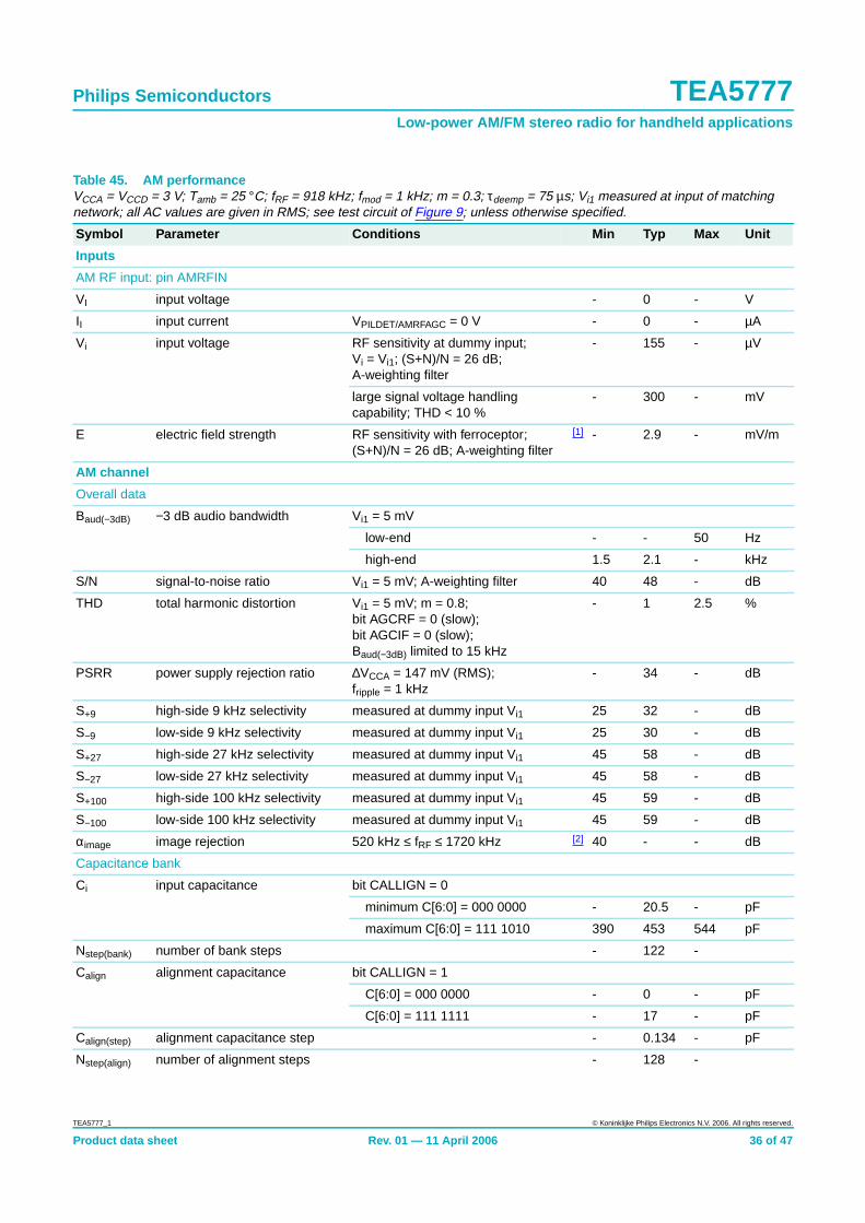
Table 45. AM performanceVCCA = VCCD = 3 V; Tamb = 25 °C; fRF = 918 kHz; fmod = 1 kHz; m = 0.3; τdeemp = 75 µs; Vi1 measured at input of matchingnetwork; all AC values are given in RMS; see test circuit of Figure 9; unless otherwise specified.
Symbol Parameter Conditions Min Typ Max Unit
Inputs
AM RF input: pin AMRFIN
VI input voltage - 0 - V
II input current VPILDET/AMRFAGC = 0 V - 0 - µA
Vi input voltage RF sensitivity at dummy input;Vi = Vi1; (S+N)/N = 26 dB;A-weighting filter
- 155 - µV
large signal voltage handlingcapability; THD < 10 %
- 300 - mV
E electric field strength RF sensitivity with ferroceptor;(S+N)/N = 26 dB; A-weighting filter
[1] - 2.9 - mV/m
AM channel
Overall data
Baud(−3dB) −3 dB audio bandwidth Vi1 = 5 mV
low-end - - 50 Hz
high-end 1.5 2.1 - kHz
S/N signal-to-noise ratio Vi1 = 5 mV; A-weighting filter 40 48 - dB
THD total harmonic distortion Vi1 = 5 mV; m = 0.8;bit AGCRF = 0 (slow);bit AGCIF = 0 (slow);Baud(−3dB) limited to 15 kHz
- 1 2.5 %
PSRR power supply rejection ratio ∆VCCA = 147 mV (RMS);fripple = 1 kHz
- 34 - dB
S+9 high-side 9 kHz selectivity measured at dummy input Vi1 25 32 - dB
S−9 low-side 9 kHz selectivity measured at dummy input Vi1 25 30 - dB
S+27 high-side 27 kHz selectivity measured at dummy input Vi1 45 58 - dB
S−27 low-side 27 kHz selectivity measured at dummy input Vi1 45 58 - dB
S+100 high-side 100 kHz selectivity measured at dummy input Vi1 45 59 - dB
S−100 low-side 100 kHz selectivity measured at dummy input Vi1 45 59 - dB
αimage image rejection 520 kHz ≤ fRF ≤ 1720 kHz [2] 40 - - dB
Capacitance bank
Ci input capacitance bit CALLIGN = 0
minimum C[6:0] = 000 0000 - 20.5 - pF
maximum C[6:0] = 111 1010 390 453 544 pF
Nstep(bank) number of bank steps - 122 -
Calign alignment capacitance bit CALLIGN = 1
C[6:0] = 000 0000 - 0 - pF
C[6:0] = 111 1111 - 17 - pF
Calign(step) alignment capacitance step - 0.134 - pF
Nstep(align) number of alignment steps - 128 -
TEA5777_1 © Koninklijke Philips Electronics N.V. 2006. All rights reserved.
Product data sheet Rev. 01 — 11 April 2006 36 of 47

Philips Semiconductors TEA5777Low-power AM/FM stereo radio for handheld applications
[1] With ferroceptor C8E-A0424 TOKO Inc.
[2] Without antenna input contribution.
LNA
GLNA LNA gain bit LNA = 0 (5 ×) - 14 - dB
bit LNA = 1 (10 ×) - 20 - dB
αAGC(RF) RF AGC attenuation VPILDET/AMRFAGC = 0 V - 0 - dB
VPILDET/AMRFAGC = 2 V - 25 - dB
Ri input resistance bit LNA = 0 (5 ×)
RFB = 0 (low feed-back) - 166 - kΩ
RFB = 1 (high feed-back) - 366 - kΩ
bit LNA = 1 (10 ×)
RFB = 0 (low feed-back) - 91 - kΩ
RFB = 1 (high feed-back) - 200 - kΩ
I and Q channel IF filter
fIF IF frequency - 21 - kHz
∆fIF IF frequency deviation - - 0.2 kHz
BIF IF filter bandwidth - 8 - kHz
Outputs
AF output: pins VAFL and VAFR
Vo(AF) AF output voltage Vi1 = 5 mV 72 90 108 mV
VO output voltage properly tuned 0.55 0.65 0.75 V
Zo output impedance 300 500 800 Ω
AM IF level detector
Input AM dummy
Vi input voltage Vi = Vi2 = detector level voltage;LNA = 1 and RFB = 0
start ADC - 50 - µV
end ADC - 2 - mV
Level output: pin TMUTE
VO output voltage Vi1 = 0 V 0.1 0.15 0.3 V
Vi1 = 10 mV 0.8 1 1.2 V
Vo(slope) output voltage slope 100 µV< Vi1 < 1 mV - 375 - mV/20dB
Zo output impedance 260 360 480 kΩ
Table 45. AM performance …continuedVCCA = VCCD = 3 V; Tamb = 25 °C; fRF = 918 kHz; fmod = 1 kHz; m = 0.3; τdeemp = 75 µs; Vi1 measured at input of matchingnetwork; all AC values are given in RMS; see test circuit of Figure 9; unless otherwise specified.
Symbol Parameter Conditions Min Typ Max Unit
TEA5777_1 © Koninklijke Philips Electronics N.V. 2006. All rights reserved.
Product data sheet Rev. 01 — 11 April 2006 37 of 47

Philips Semiconductors TEA5777Low-power AM/FM stereo radio for handheld applications
Table 46. Stereo decoder characteristicsVCCA = VCCD = 3 V; Tamb = 25 °C; τdeemp= 50 µs; not forced to mono; all AC values are given in RMS; see test circuit ofFigure 9; unless otherwise specified.
Symbol Parameter Conditions Min Typ Max Unit
Input: pin MPXIN
VI input voltage 0.7 0.75 0.8 V
Ri input resistance 300 400 500 kΩ
MPX stereo decoder channel
Overall data
Gv voltage gain fmod = 1 kHz [1] −1.1 −0.82 −0.4 dB
αcs channel separation Vi3 = 300 mV; fmod = 1 kHz;Vpilot = 30 mV; R = 1 and L = 0 orR = 0 and L = 1; VTMUTE = 1 V;fIF = 133.333 kHz; Baud(−3dB)limited to 15 kHz
26 40 - dB
(S+N)/N signal plus noise-to-noise ratio measured at AF output; L = R;Vi3 = 300 mV; fmod = 1 kHz;Vpilot = 30 mV; A-weighted
- 68.5 - dB
THD total harmonic distortion measured at AF output; L = R;VMPXOUT = 300 mV; fmod = 1 kHz;Vpilot = 30 mV; Baud(−3dB) limited to15 kHz
- 0.05 0.5 %
α19 19 kHz suppression reference 300 mV = 0 dB 23 28 - dB
α38 38 kHz suppression reference 300 mV = 0 dB 31 52 - dB
Pilot detector
Vpilot pilot voltage VTMUTE = 1 V
switching to stereo - 13 16 mV
switching back to mono 3 6 - mV
mono hysteresis 6 7 8 mV
Integrated de-emphasis
τdeemp de-emphasis time constant bit DEEM = 0 - 50 - µs
bit DEEM = 1 - 75 - µs
Hard mute
αmute mute attenuation measured on pins VAFL andVAFR; audio muted with bitMUTE = 1; A-weighted
60 70 - dB
SDS curve (blend function)
Vi input voltage SDS region voltage Vi = Vi1;Vi3 = 300 mV; fmod = 1 kHz;Vpilot = 30 mV; R = 1 and L = 0 orR = 0 and L = 1; bit SDSOFF = 0;bit DOFF = 0; bit FOMO = 0
start level - 15 - µV
stop level - 150 - µV
TEA5777_1 © Koninklijke Philips Electronics N.V. 2006. All rights reserved.
Product data sheet Rev. 01 — 11 April 2006 38 of 47

Philips Semiconductors TEA5777Low-power AM/FM stereo radio for handheld applications
[1] This includes the attenuation due to the de-emphasis. At 1 kHz this is approximately 0.4 dB for 50 µs.
AF output: pins VAFL and VAFR
Vo(AF) AF output voltage measured with respect to input pinMPXIN; Vi3 = 100 mV; L = R;fmod = 1 kHz
83 91 99 mV
Io(sink)M peak sink output current Vi3 = 100 mV; L = R; fmod = 1 kHz - 60 - µA
VO output voltage measured with respect to input pinMPXIN; FM mode
0.675 0.75 0.825 V
Ro output resistance 300 500 800 Ω
Table 46. Stereo decoder characteristics …continuedVCCA = VCCD = 3 V; Tamb = 25 °C; τdeemp= 50 µs; not forced to mono; all AC values are given in RMS; see test circuit ofFigure 9; unless otherwise specified.
Symbol Parameter Conditions Min Typ Max Unit
TEA5777_1 © Koninklijke Philips Electronics N.V. 2006. All rights reserved.
Product data sheet Rev. 01 — 11 April 2006 39 of 47
Philips Semiconductors TEA5777Low-power AM/FM stereo radio for handheld applications
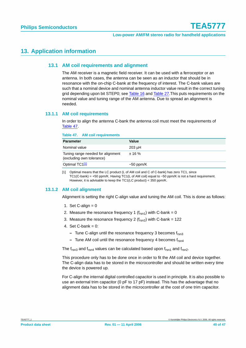
13. Application information
13.1 AM coil requirements and alignmentThe AM receiver is a magnetic field receiver. It can be used with a ferroceptor or anantenna. In both cases, the antenna can be seen as an inductor that should be inresonance with the on-chip C-bank at the frequency of interest. The C-bank values aresuch that a nominal device and nominal antenna inductor value result in the correct tuninggrid depending upon bit STEP0; see Table 16 and Table 27.This puts requirements on thenominal value and tuning range of the AM antenna. Due to spread an alignment isneeded.
13.1.1 AM coil requirements
In order to align the antenna C-bank the antenna coil must meet the requirements ofTable 47.
[1] Optimal means that the LC product (L of AM coil and C of C-bank) has zero TC1, sinceTC1(C-bank) = +50 ppm/K. Having TC1(L of AM coil) equal to −50 ppm/K is not a hard requirement.However, it is advisable to keep the TC1(LC product) < 350 ppm/K.
13.1.2 AM coil alignment
Alignment is setting the right C-align value and tuning the AM coil. This is done as follows:
1. Set C-align = 0
2. Measure the resonance frequency 1 (frsn1) with C-bank = 0
3. Measure the resonance frequency 2 (frsn2) with C-bank = 122
4. Set C-bank = 0:
– Tune C-align until the resonance frequency 3 becomes frsn3
– Tune AM coil until the resonance frequency 4 becomes frsn4
The frsn3 and frsn4 values can be calculated based upon frsn1 and frsn2.
This procedure only has to be done once in order to fit the AM coil and device together.The C-align data has to be stored in the microcontroller and should be written every timethe device is powered up.
For C-align the internal digital controlled capacitor is used in principle. It is also possible touse an external trim capacitor (0 pF to 17 pF) instead. This has the advantage that noalignment data has to be stored in the microcontroller at the cost of one trim capacitor.
Table 47. AM coil requirements
Parameter Value
Nominal value 203 µH
Tuning range needed for alignment(excluding own tolerance)
± 16 %
Optimal TC1[1] −50 ppm/K
TEA5777_1 © Koninklijke Philips Electronics N.V. 2006. All rights reserved.
Product data sheet Rev. 01 — 11 April 2006 40 of 47

xxxx xxxxxxxxxxxxxxxxxxxxxxxxxxxxxx x xxxxxxxxxxxxxx xxxxxxxxxx xxx xxxxxx xxxxxxxxxxxxxxxxxxxxxxx xxxxxxxxxxxxxxxxxxxxxxxxxxx xxxxxx xx xxxxxxxxxxxxxxxxxxxxxxxxxxxxx xxxxxxxxxxxxxxxxxxxxxx xxxxxxxxxxx xxxxxxx xxxxxxxxxxxxxxxxxxxxxxxxxxxxxxxxxxx xxxxxxxxxxxxxx xxxxxx xx xxxxxxxxxxxxxxxxxxxxxxxxxxxxxxxx xxxxxxxxxxxxxxxxxxxxxxxx xxxxxxxxxxxxxxxxxxxxxxxxxxxxxxxxxxxxxxxxxxxxxxxxxxxxx xxxxxxxxxxx xxxxx x x
TE
A5777_1
Product data shee
Philips S
emiconduc
14.Test inform
at
R LVi3
audio
t
OU
T
R IN L DIG A 2C
AP
F
C10 C20C7 C1
torsT
EA
5777Low
-power A
M/F
M stereo radio for handheld applications
ion
001aab437
E
E_READ
K
R10
C21
C6
X140 MHz
write/read
buscontroldata
clock
VCC
C19
VCCR8
© K
oninklijke Philips E
lectronics N.V. 2006. A
ll rights reserved.
Rev. 01 —
11 April 2006
41 of 47 Fig 9. Test circuit
TEA5777HL
BUSMODE
MP
X
VA
F
MP
X
VA
F
V25
GN
D
AG
C
VR
E
CP
OU
T
VC
OTA
NK
1
VC
OTA
NK
2
GN
DV
CO
_AM
RF
AM
RF
IN
SW
PO
RT
1
VC
CD
SW
PO
RT
2/E
XT
IN
V25IF
GNDIF
RFIN1
GNDRF
RFIN2
PILDET/AMRFAGC
VAMLNA
VCCA
TMUT
WRIT
DATA
CLOC
XTAL1
GNDD
XTAL2
VCC
C5
C14
C15
L1 L2
D9D8R4
C12
C11
L6
R14
50 Ω
AM dummy
Vi1
Vi(ext)
Vi2
R15
C17L3
C16
C18L4R13
R1250 Ω
FM dummy
R11
1
25
32
30
29
31
27
26
28
16
9
11
12
10
14
15
13
2 3 4 5 6 7 8
24 23 22 21 20 19 18 17

Philips Semiconductors TEA5777Low-power AM/FM stereo radio for handheld applications
Table 48. Test circuit components
Partnumber
Specification Remark
Value Tolerance Type
C1 100 nF 20 % C0603
C5 3.3 µF 20 % 6V3 B45196E1335M10*, EPCOS
C6 100 nF 20 % C0603
C7 2.2 µF 20 % 6V3 B45196E1225M10*, EPCOS
C10 220 nF 20 % C0805
C11 15 nF 20 % C0603
C12 220 nF 20 % C0805
C14 1 µF 20 % C1206 low leakage (< 5 nA), X7R
C15 3.3 µF 20 % 6V3 B45196E1335M10*, EPCOS
C16 33 pF 5 % C0603 NP0
C17 39 pF 5 % C0603 NP0
C18 12 pF 5 % C0603 NP0
C19 2.2 µF 20 % 6V3 B45196E1225M10*, EPCOS
C20 220 nF 20 % C0603 NP0
C21 1 µF 20 % 16 V B45196E3105M10*, EPCOS
D8 BB202
D9 BB202
L1 33 nH 5 % Q = 40 TOKO, LLQ1608-A33N_J
L2 33 nH 5 % Q = 40 TOKO, LLQ1608-A33N_J
L3 120 nH 5 % TOKO, LLQ1608-AR120N_J
L4 220 nH 5 % TOKO, LLQ1608-AR220N_J
L6 200 nH Q > 120 tuning range larger than −16 % to +16 %;Sagami 940927266B (part of the AM dummy)
R4 2.2 kΩ 20 % R0603
R8 100 W 20 % R0603
R10 47 W 20 % R0603
R11 10 W 5 % R0603 (part of the FM dummy, i.e. 50 Ω to 75 Ω)
R12 60 W 5 % R0603 (part of the FM dummy, i.e. 50 Ω to 75 Ω)
R13 45 W 5 % R0603 (part of the FM dummy, i.e. 50 Ω to 75 Ω)
R14 51 W 5 % R0603 (part of the AM dummy)
R15 1 W 5 % R0603 (part of the AM dummy)
X1 4 MHz HC49 NDK
TEA5777_1 © Koninklijke Philips Electronics N.V. 2006. All rights reserved.
Product data sheet Rev. 01 — 11 April 2006 42 of 47

Philips Semiconductors TEA5777Low-power AM/FM stereo radio for handheld applications
15. Package outline
Fig 10. Package outline SOT619-1 (HVQFN48)
0.51
A1 EhbUNIT ye
0.2
c
REFERENCESOUTLINEVERSION
EUROPEANPROJECTION ISSUE DATE
IEC JEDEC JEITA
mm 7.16.9
Dh
5.254.95
y1
7.16.9
5.254.95
e1
5.5
e2
5.50.300.18
0.050.00
0.05 0.1
DIMENSIONS (mm are the original dimensions)
SOT619-1 MO-220 - - -- - -
0.50.3
L
0.1
v
0.05
w
0 2.5 5 mm
scale
SOT619-1HVQFN48: plastic thermal enhanced very thin quad flat package; no leads;48 terminals; body 7 x 7 x 0.85 mm
A(1)
max.
AA1
c
detail X
yy1 Ce
L
Eh
Dh
e
e1
b
13 24
48 37
36
2512
1
X
D
E
C
B A
e2
01-08-0802-10-18
terminal 1index area
terminal 1index area
1/2 e
1/2 e ACC
Bv M
w M
E(1)
Note
1. Plastic or metal protrusions of 0.075 mm maximum per side are not included.
D(1)
TEA5777_1 © Koninklijke Philips Electronics N.V. 2006. All rights reserved.
Product data sheet Rev. 01 — 11 April 2006 43 of 47

Philips Semiconductors TEA5777Low-power AM/FM stereo radio for handheld applications
Fig 11. Package outline SOT358-1 (LQFP32)
UNITA
max. A1 A2 A3 bp c E(1) e HE L L p Zywv θ
REFERENCESOUTLINEVERSION
EUROPEANPROJECTION ISSUE DATE
IEC JEDEC JEITA
mm 1.60.200.05
1.451.35
0.250.40.3
0.180.12
7.16.9
0.89.158.85
0.90.5
70
o
o0.25 0.11 0.2
DIMENSIONS (mm are the original dimensions)
Note
1. Plastic or metal protrusions of 0.25 mm maximum per side are not included.
0.750.45
SOT358 -1 136E03 MS-02603-02-2505-11-09
D(1) (1)(1)
7.16.9
HD
9.158.85
EZ
0.90.5
D
bp
e
θ
EA1
A
Lp
detail X
L
(A )3
B
8
c
DH
bp
EH A2
v M B
D
ZD
A
ZE
e
v M A
X
1
32
25
24 17
16
9
y
pin 1 index
w M
w M
0 2.5 5 mm
scale
LQFP32: plastic low profile quad flat package; 32 leads; body 7 x 7 x 1.4 mm SOT358-1
TEA5777_1 © Koninklijke Philips Electronics N.V. 2006. All rights reserved.
Product data sheet Rev. 01 — 11 April 2006 44 of 47
Philips Semiconductors TEA5777Low-power AM/FM stereo radio for handheld applications
16. Abbreviations
17. Revision history
Table 49. Abbreviations
Acronym Description
ADC Analog-to-Digital Converter
AGC Automatic Gain Control
BiCMOS Bi-polar Complementary Metal-Oxide Semiconductor
FET Field-Effect Transistor
GSM Global System for Mobile communication
HBM Human Body Model
I/Q In-phase/Quadrature-phase
LNA Low Noise Amplifier
LW Long Wave
MOSFET Metal-Oxide-Semiconductor Field-Effect Transistor
MPX Multiplex
MM Machine Model
MW Medium Wave
OIRT Organisation Internationale de Radiodiffusion et de Télévision (InternationalRadio and Television Organization)
PLL Phase-Locked Loop
RDS Radio Data System
RSSI Receiver Signal Strength Information
SDS Signal Dependent Stereo
VCO Voltage Controlled Oscillator
Table 50. Revision history
Document ID Release date Data sheet status Change notice Supersedes
TEA5777_1 20060411 Product data sheet - -
TEA5777_1 © Koninklijke Philips Electronics N.V. 2006. All rights reserved.
Product data sheet Rev. 01 — 11 April 2006 45 of 47

Philips Semiconductors TEA5777Low-power AM/FM stereo radio for handheld applications
18. Legal information
18.1 Data sheet status
[1] Please consult the most recently issued document before initiating or completing a design.
[2] The term ‘short data sheet’ is explained in section “Definitions”.
[3] The product status of device(s) described in this document may have changed since this document was published and may differ in case of multiple devices. The latest product statusinformation is available on the Internet at URL http://www.semiconductors.philips.com.
18.2 Definitions
Draft — The document is a draft version only. The content is still underinternal review and subject to formal approval, which may result inmodifications or additions. Philips Semiconductors does not give anyrepresentations or warranties as to the accuracy or completeness ofinformation included herein and shall have no liability for the consequences ofuse of such information.
Short data sheet — A short data sheet is an extract from a full data sheetwith the same product type number(s) and title. A short data sheet is intendedfor quick reference only and should not be relied upon to contain detailed andfull information. For detailed and full information see the relevant full datasheet, which is available on request via the local Philips Semiconductorssales office. In case of any inconsistency or conflict with the short data sheet,the full data sheet shall prevail.
18.3 Disclaimers
General — Information in this document is believed to be accurate andreliable. However, Philips Semiconductors does not give any representationsor warranties, expressed or implied, as to the accuracy or completeness ofsuch information and shall have no liability for the consequences of use ofsuch information.
Right to make changes — Philips Semiconductors reserves the right tomake changes to information published in this document, including withoutlimitation specifications and product descriptions, at any time and withoutnotice. This document supersedes and replaces all information supplied priorto the publication hereof.
Suitability for use — Philips Semiconductors products are not designed,authorized or warranted to be suitable for use in medical, military, aircraft,space or life support equipment, nor in applications where failure ormalfunction of a Philips Semiconductors product can reasonably be expected
to result in personal injury, death or severe property or environmentaldamage. Philips Semiconductors accepts no liability for inclusion and/or useof Philips Semiconductors products in such equipment or applications andtherefore such inclusion and/or use is at the customer’s own risk.
Applications — Applications that are described herein for any of theseproducts are for illustrative purposes only. Philips Semiconductors makes norepresentation or warranty that such applications will be suitable for thespecified use without further testing or modification.
Limiting values — Stress above one or more limiting values (as defined inthe Absolute Maximum Ratings System of IEC 60134) may cause permanentdamage to the device. Limiting values are stress ratings only and operation ofthe device at these or any other conditions above those given in theCharacteristics sections of this document is not implied. Exposure to limitingvalues for extended periods may affect device reliability.
Terms and conditions of sale — Philips Semiconductors products are soldsubject to the general terms and conditions of commercial sale, as publishedat http://www.semiconductors.philips.com/profile/terms, including thosepertaining to warranty, intellectual property rights infringement and limitationof liability, unless explicitly otherwise agreed to in writing by PhilipsSemiconductors. In case of any inconsistency or conflict between informationin this document and such terms and conditions, the latter will prevail.
No offer to sell or license — Nothing in this document may be interpretedor construed as an offer to sell products that is open for acceptance or thegrant, conveyance or implication of any license under any copyrights, patentsor other industrial or intellectual property rights.
18.4 TrademarksNotice: All referenced brands, product names, service names and trademarksare the property of their respective owners.
I2C-bus — logo is a trademark of Koninklijke Philips Electronics N.V.
19. Contact information
For additional information, please visit: http://www.semiconductors.philips.com
For sales office addresses, send an email to: [email protected]
Document status [1] [2] Product status [3] Definition
Objective [short] data sheet Development This document contains data from the objective specification for product development.
Preliminary [short] data sheet Qualification This document contains data from the preliminary specification.
Product [short] data sheet Production This document contains the product specification.
TEA5777_1 © Koninklijke Philips Electronics N.V. 2006. All rights reserved.
Product data sheet Rev. 01 — 11 April 2006 46 of 47

Philips Semiconductors TEA5777Low-power AM/FM stereo radio for handheld applications
20. Contents
1 General description . . . . . . . . . . . . . . . . . . . . . . 12 Features . . . . . . . . . . . . . . . . . . . . . . . . . . . . . . . 12.1 General . . . . . . . . . . . . . . . . . . . . . . . . . . . . . . . 12.2 AM . . . . . . . . . . . . . . . . . . . . . . . . . . . . . . . . . . 12.3 FM. . . . . . . . . . . . . . . . . . . . . . . . . . . . . . . . . . . 23 Applications . . . . . . . . . . . . . . . . . . . . . . . . . . . . 24 Quick reference data . . . . . . . . . . . . . . . . . . . . . 25 Ordering information . . . . . . . . . . . . . . . . . . . . . 46 Block diagram . . . . . . . . . . . . . . . . . . . . . . . . . . 57 Pinning information . . . . . . . . . . . . . . . . . . . . . . 67.1 Pinning . . . . . . . . . . . . . . . . . . . . . . . . . . . . . . . 67.2 Pin description . . . . . . . . . . . . . . . . . . . . . . . . . 78 Functional description . . . . . . . . . . . . . . . . . . . 98.1 AM radio part . . . . . . . . . . . . . . . . . . . . . . . . . 108.1.1 AM RF amplifier . . . . . . . . . . . . . . . . . . . . . . . 108.1.2 Tuning AM antenna circuit . . . . . . . . . . . . . . . 108.1.3 AM I/Q mixer. . . . . . . . . . . . . . . . . . . . . . . . . . 108.1.4 AM VCO . . . . . . . . . . . . . . . . . . . . . . . . . . . . . 108.1.5 AM IF filter . . . . . . . . . . . . . . . . . . . . . . . . . . . 118.1.6 AM IF amplification and AM detection . . . . . . 118.2 FM radio part . . . . . . . . . . . . . . . . . . . . . . . . . 118.2.1 Low noise RF amplifier . . . . . . . . . . . . . . . . . . 118.2.2 FM I/Q mixer . . . . . . . . . . . . . . . . . . . . . . . . . . 118.2.3 FM VCO . . . . . . . . . . . . . . . . . . . . . . . . . . . . . 128.2.4 FM IF filter. . . . . . . . . . . . . . . . . . . . . . . . . . . . 128.2.5 FM demodulator . . . . . . . . . . . . . . . . . . . . . . . 128.3 Stereo decoder . . . . . . . . . . . . . . . . . . . . . . . . 128.3.1 MPX decoder . . . . . . . . . . . . . . . . . . . . . . . . . 128.3.2 Signal strength depending mono/stereo blend 128.3.3 Pilot detector. . . . . . . . . . . . . . . . . . . . . . . . . . 128.3.4 De-emphasis. . . . . . . . . . . . . . . . . . . . . . . . . . 128.4 Tuning function . . . . . . . . . . . . . . . . . . . . . . . . 128.4.1 Reference frequency generation . . . . . . . . . . 138.4.2 Crystal oscillator . . . . . . . . . . . . . . . . . . . . . . . 138.4.3 IF counter . . . . . . . . . . . . . . . . . . . . . . . . . . . . 138.4.4 Automatic search operation . . . . . . . . . . . . . . 138.5 RF level information (RSSI) . . . . . . . . . . . . . . 148.6 Software programmable ports . . . . . . . . . . . . 149 Control functions via I 2C-bus and 3-wire bus 159.1 Bus interface. . . . . . . . . . . . . . . . . . . . . . . . . . 159.2 Bus protocol . . . . . . . . . . . . . . . . . . . . . . . . . . 159.3 I2C-bus mode . . . . . . . . . . . . . . . . . . . . . . . . . 169.3.1 Write mode . . . . . . . . . . . . . . . . . . . . . . . . . . . 169.3.2 Read mode . . . . . . . . . . . . . . . . . . . . . . . . . . . 179.3.3 Dbus function in I2C-bus mode (silent readout) 179.4 3-wire bus mode . . . . . . . . . . . . . . . . . . . . . . . 18
9.4.1 Write mode. . . . . . . . . . . . . . . . . . . . . . . . . . . 189.4.2 Read mode. . . . . . . . . . . . . . . . . . . . . . . . . . . 199.4.3 Dbus function in 3-wire mode (silent readout) 199.5 Data transfer in I2C-bus and 3-wire mode . . . 209.5.1 Register definition in write mode . . . . . . . . . . 209.5.1.1 FM write mode . . . . . . . . . . . . . . . . . . . . . . . . 209.5.1.2 AM write mode . . . . . . . . . . . . . . . . . . . . . . . . 229.5.2 Register definition in read mode . . . . . . . . . . 259.5.2.1 FM read mode . . . . . . . . . . . . . . . . . . . . . . . . 259.5.2.2 AM read mode . . . . . . . . . . . . . . . . . . . . . . . . 2610 Limiting values . . . . . . . . . . . . . . . . . . . . . . . . 2811 Thermal characteristics . . . . . . . . . . . . . . . . . 2812 Characteristics . . . . . . . . . . . . . . . . . . . . . . . . 2913 Application information . . . . . . . . . . . . . . . . . 4013.1 AM coil requirements and alignment . . . . . . . 4013.1.1 AM coil requirements . . . . . . . . . . . . . . . . . . . 4013.1.2 AM coil alignment. . . . . . . . . . . . . . . . . . . . . . 4014 Test information. . . . . . . . . . . . . . . . . . . . . . . . 4115 Package outline . . . . . . . . . . . . . . . . . . . . . . . . 4316 Abbreviations . . . . . . . . . . . . . . . . . . . . . . . . . 4517 Revision history . . . . . . . . . . . . . . . . . . . . . . . 4518 Legal information . . . . . . . . . . . . . . . . . . . . . . 4618.1 Data sheet status . . . . . . . . . . . . . . . . . . . . . . 4618.2 Definitions . . . . . . . . . . . . . . . . . . . . . . . . . . . 4618.3 Disclaimers. . . . . . . . . . . . . . . . . . . . . . . . . . . 4618.4 Trademarks . . . . . . . . . . . . . . . . . . . . . . . . . . 4619 Contact information . . . . . . . . . . . . . . . . . . . . 4620 Contents. . . . . . . . . . . . . . . . . . . . . . . . . . . . . . 47
© Koninklijke Philips Electronics N.V. 2006. All rights reserved.For more information, please visit: http://www.semiconductors.philips.com.For sales office addresses, email to: [email protected].
Date of release: 11 April 2006
Document identifier: TEA5777_1
Please be aware that important notices concerning this document and the product(s)described herein, have been included in section ‘Legal information’.