TCAD Analysis of Silicon-Germanium (SiGe) based Back ...
4
TCAD Analysis of Silicon-Germanium (SiGe) based Back-Contact Back-Junction (BC-BJ) solar cell as an alternative for silicon based cells R. Pandey* and R. Chaujar** Microelectronics Research Lab, Department of Engineering Physics, Delhi Technological University, Bawana Road, Delhi-110042, India *[email protected] **[email protected] ABSTRACT In this work, an ultra-thin, Back-Contact Back-Junction (BC-BJ) Silicon-Germanium (SiGe) solar cell device structure called BC-BJ SiGe solar cell has been proposed, which shows enhanced photovoltaic properties, External Quantum Efficiency (EQE) > 76% in the spectrum range of 400-700 nm wavelength have been achieved. Results further, reveal that proposed device is less affected by carrier recombination, resulting in 13.5 % power conversion efficiency (PCE). Also we obtained the impact of material thickness on device parameters and we found that the 5μm thick SiGe cell is as efficient as 10μm thick silicon cell. The PCE of 5μm thick SiGe cell and 10μm thick silicon cell was 11.3% and 11.8%, respectively. It indicates that the proposed device significantly save the material cost over the silicon cell. All the simulations have been done using DEVEDIT and ATLAS device simulator. Keywords: Efficiency, Recombination, Silicon-Germanim, Solar cell 1 INTRODUCTION Crystalline silicon is the largest component of the solar photovoltaic (PV) cells. Over 80% installed solar PV in 2011 used silicon as their largest material. Silicon is widely used material for PV due to its reliability, abundance, and mature fabrication process. In Silicon PV technology, absorption coefficient of Silicon is small, to absorb enough of the solar cell spectrum. The thickness of conventional silicon cell is typically more than 100μm, in order to absorb the solar spectrum. Now since, thickness is large, in order to collect light generated carrier, minority carrier lifetime must be high enough and the recombination coefficient should be low. This requirement of large volume and high quality silicon significantly increases the module cost. In order to make photovoltaic system feasible at large scale, it should be cost effective, with module cost to be < $0.5/W [1]. In this paper, we proposed SiGe as an alternative to silicon solar cell, due to its higher minority carrier lifetime and lower recombination coefficient. Reducing the thickness of PV materials used in solar cell production is a major goal of solar cell industry, due to its fruitful contribution to the overall cost of a PV system. However, thin silicon cells are not effective, due to severe Auger recombination and increased surface to volume ratio [2]. One promising high-efficiency solar cell concept is the back-contact back- junction solar cell [3, 4] having both, junction and the electrodes at back side of the device. Now, since the junction and contacts are at the back side, Front surface can be designed for optimum optical performance [5]. Here, we proposed novel 10μm thick crystalline SiGe back-contact back-junction solar cell, which overcomes the critical problems of thin devices: Auger and surface recombination etc. Further, we have obtained the impact of material thickness on photovoltaic parameters. In SiGe technology the electrical properties of silicon are modified with germanium. SiGe processing is simple because the physical and electrical properties of silicon and germanium are similar [6]. Also SiGe possesses higher mechanical strength, and suppresses the high intensity degradation of solar cell under illumination [7]. Optical absorption of SiGe can further be modified by varying Ge content [8, 9]. 2 DEVICE STRUCTURE AND PHYSICAL MODELS Silvaco ATLAS used to simulate the device optoelectronic characteristics. ATLAS is a device simulator capable of modeling the electrical, thermal, and optical characteristics of semiconductor devices. In the simulation, we assume a two dimensional structure, BC-BJ solar cell as shown in Fig. 1. The Si0.9 Ge0.1 was used during the simulation, very small fraction of germanium is used. Because, if we increase the germanium content the bandgap of SiGe decreases [10] The substrate was N-type, with doping density of 3x10 15 cm -3 , whereas N+/P+ region has the doping density of 4x10 20 cm -3 . The depth of P+ and N+ region was 3μm and 2.5μm, respectively, whereas the width was 40μm and 30μm, respectively. The Nitride (Si3N4) is used as anti-reflecting front surface passivation, and modeled as an optical layer with the thickness of 70 nm. The Oxide (SiO2) is used as back surface passivation with thickness of 50nm. 199 Materials for Energy, Efficiency and Sustainability: TechConnect Briefs 2015
Transcript of TCAD Analysis of Silicon-Germanium (SiGe) based Back ...

TCAD Analysis of Silicon-Germanium (SiGe) based Back-Contact Back-Junction
(BC-BJ) solar cell as an alternative for silicon based cells
R. Pandey* and R. Chaujar**
Microelectronics Research Lab, Department of Engineering Physics,
Delhi Technological University, Bawana Road, Delhi-110042, India
ABSTRACT
In this work, an ultra-thin, Back-Contact Back-Junction
(BC-BJ) Silicon-Germanium (SiGe) solar cell device
structure called BC-BJ SiGe solar cell has been proposed,
which shows enhanced photovoltaic properties, External
Quantum Efficiency (EQE) > 76% in the spectrum range of
400-700 nm wavelength have been achieved. Results
further, reveal that proposed device is less affected by
carrier recombination, resulting in 13.5 % power conversion
efficiency (PCE). Also we obtained the impact of material
thickness on device parameters and we found that the 5µm
thick SiGe cell is as efficient as 10µm thick silicon cell. The
PCE of 5µm thick SiGe cell and 10µm thick silicon cell was
11.3% and 11.8%, respectively. It indicates that the
proposed device significantly save the material cost over the
silicon cell. All the simulations have been done using
DEVEDIT and ATLAS device simulator.
Keywords: Efficiency, Recombination, Silicon-Germanim,
Solar cell
1 INTRODUCTION
Crystalline silicon is the largest component of the solar
photovoltaic (PV) cells. Over 80% installed solar PV in
2011 used silicon as their largest material. Silicon is widely
used material for PV due to its reliability, abundance, and
mature fabrication process. In Silicon PV technology,
absorption coefficient of Silicon is small, to absorb enough
of the solar cell spectrum. The thickness of conventional
silicon cell is typically more than 100µm, in order to absorb
the solar spectrum. Now since, thickness is large, in order to
collect light generated carrier, minority carrier lifetime must
be high enough and the recombination coefficient should be
low. This requirement of large volume and high quality
silicon significantly increases the module cost. In order to
make photovoltaic system feasible at large scale, it should
be cost effective, with module cost to be < $0.5/W [1]. In
this paper, we proposed SiGe as an alternative to silicon
solar cell, due to its higher minority carrier lifetime and
lower recombination coefficient. Reducing the thickness of
PV materials used in solar cell production is a major goal of
solar cell industry, due to its fruitful contribution to the
overall cost of a PV system. However, thin silicon cells are
not effective, due to severe Auger recombination and
increased surface to volume ratio [2].
One promising high-efficiency solar cell concept is the
back-contact back- junction solar cell [3, 4] having both,
junction and the electrodes at back side of the device. Now,
since the junction and contacts are at the back side, Front
surface can be designed for optimum optical performance
[5].
Here, we proposed novel 10µm thick crystalline SiGe
back-contact back-junction solar cell, which overcomes the
critical problems of thin devices: Auger and surface
recombination etc. Further, we have obtained the impact of
material thickness on photovoltaic parameters. In SiGe
technology the electrical properties of silicon are modified
with germanium. SiGe processing is simple because the
physical and electrical properties of silicon and germanium
are similar [6]. Also SiGe possesses higher mechanical
strength, and suppresses the high intensity degradation of
solar cell under illumination [7]. Optical absorption of SiGe
can further be modified by varying Ge content [8, 9].
2 DEVICE STRUCTURE AND PHYSICAL
MODELS
Silvaco ATLAS used to simulate the device
optoelectronic characteristics. ATLAS is a device simulator
capable of modeling the electrical, thermal, and optical
characteristics of semiconductor devices.
In the simulation, we assume a two dimensional
structure, BC-BJ solar cell as shown in Fig. 1. The Si0.9
Ge0.1 was used during the simulation, very small fraction of
germanium is used. Because, if we increase the germanium
content the bandgap of SiGe decreases [10] The substrate
was N-type, with doping density of 3x1015 cm-3, whereas
N+/P+ region has the doping density of 4x1020 cm-3. The
depth of P+ and N+ region was 3µm and 2.5µm,
respectively, whereas the width was 40µm and 30µm,
respectively. The Nitride (Si3N4) is used as anti-reflecting
front surface passivation, and modeled as an optical layer
with the thickness of 70 nm. The Oxide (SiO2) is used as
back surface passivation with thickness of 50nm.
199Materials for Energy, Efficiency and Sustainability: TechConnect Briefs 2015
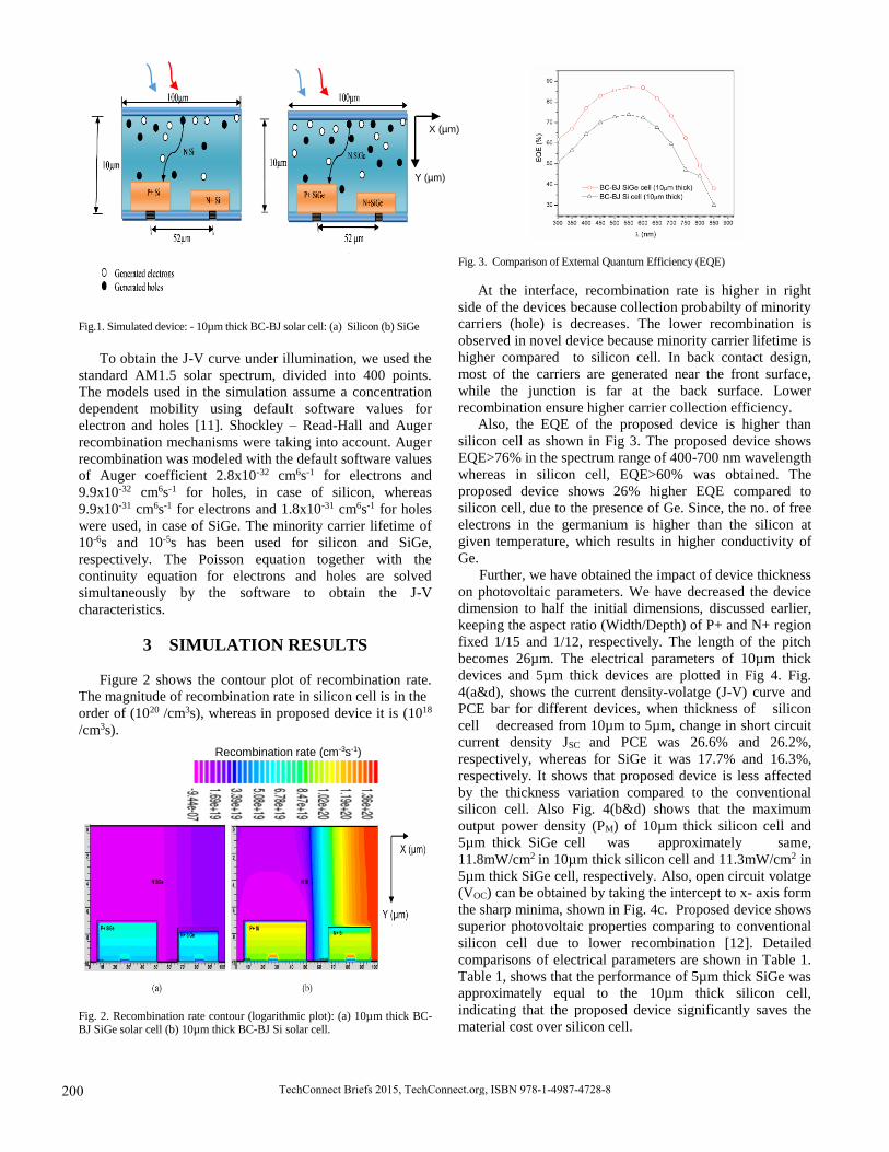
Fig.1. Simulated device: - 10µm thick BC-BJ solar cell: (a) Silicon (b) SiGe
To obtain the J-V curve under illumination, we used the
standard AM1.5 solar spectrum, divided into 400 points.
The models used in the simulation assume a concentration
dependent mobility using default software values for
electron and holes [11]. Shockley – Read-Hall and Auger
recombination mechanisms were taking into account. Auger
recombination was modeled with the default software values
of Auger coefficient 2.8x10⁻³² cm6s-1 for electrons and
9.9x10⁻³² cm6s-1 for holes, in case of silicon, whereas
9.9x10⁻³¹ cm6s-1 for electrons and 1.8x10⁻³¹ cm6s-1 for holes
were used, in case of SiGe. The minority carrier lifetime of
10-6s and 10-5s has been used for silicon and SiGe,
respectively. The Poisson equation together with the
continuity equation for electrons and holes are solved
simultaneously by the software to obtain the J-V
characteristics.
3 SIMULATION RESULTS
Figure 2 shows the contour plot of recombination rate.
The magnitude of recombination rate in silicon cell is in the
order of (1020 /cm3s), whereas in proposed device it is (1018
/cm3s).
Fig. 2. Recombination rate contour (logarithmic plot): (a) 10µm thick BC-
BJ SiGe solar cell (b) 10µm thick BC-BJ Si solar cell.
Fig. 3. Comparison of External Quantum Efficiency (EQE)
At the interface, recombination rate is higher in right
side of the devices because collection probabilty of minority
carriers (hole) is decreases. The lower recombination is
observed in novel device because minority carrier lifetime is
higher compared to silicon cell. In back contact design,
most of the carriers are generated near the front surface,
while the junction is far at the back surface. Lower
recombination ensure higher carrier collection efficiency.
Also, the EQE of the proposed device is higher than
silicon cell as shown in Fig 3. The proposed device shows
EQE>76% in the spectrum range of 400-700 nm wavelength
whereas in silicon cell, EQE>60% was obtained. The
proposed device shows 26% higher EQE compared to
silicon cell, due to the presence of Ge. Since, the no. of free
electrons in the germanium is higher than the silicon at
given temperature, which results in higher conductivity of
Ge.
Further, we have obtained the impact of device thickness
on photovoltaic parameters. We have decreased the device
dimension to half the initial dimensions, discussed earlier,
keeping the aspect ratio (Width/Depth) of P+ and N+ region
fixed 1/15 and 1/12, respectively. The length of the pitch
becomes 26µm. The electrical parameters of 10µm thick
devices and 5µm thick devices are plotted in Fig 4. Fig.
4(a&d), shows the current density-volatge (J-V) curve and
PCE bar for different devices, when thickness of silicon
cell decreased from 10µm to 5µm, change in short circuit
current density JSC and PCE was 26.6% and 26.2%,
respectively, whereas for SiGe it was 17.7% and 16.3%,
respectively. It shows that proposed device is less affected
by the thickness variation compared to the conventional
silicon cell. Also Fig. 4(b&d) shows that the maximum
output power density (PM) of 10µm thick silicon cell and
5µm thick SiGe cell was approximately same,
11.8mW/cm2 in 10µm thick silicon cell and 11.3mW/cm2 in
5µm thick SiGe cell, respectively. Also, open circuit volatge
(VOC) can be obtained by taking the intercept to x- axis form
the sharp minima, shown in Fig. 4c. Proposed device shows
superior photovoltaic properties comparing to conventional
silicon cell due to lower recombination [12]. Detailed
comparisons of electrical parameters are shown in Table 1.
Table 1, shows that the performance of 5µm thick SiGe was
approximately equal to the 10µm thick silicon cell,
indicating that the proposed device significantly saves the
material cost over silicon cell.
Y (µm)
X (µm)
Recombination rate (cm-3s-1)
200 TechConnect Briefs 2015, TechConnect.org, ISBN 978-1-4987-4728-8

Fig.4. Comparisons of electrical characteristics of different devices: (a) J-V, (b) Power density-voltage, (c) Abs.current density-
voltage (d) PCE.
Table1. Detailed comparisons of electrical parameters
4 CONCLUSION
In this work, we proposed a novel 10µm thick BC-BJ
SiGe Solar cell design, as a cost-effective solution for
energy efficient applications. The work analyse and
compares the optical and electrical characteristics of
proposed design using Silvaco Atlas device simulator.
Proposed device shows superior photovoltaic parameters
compared to silicon cell. Also results reveal that when
the
thickness of proposed device is reduced to 5µm, its PCE,
11.3% was approximately equal to PCE, 11.8% of 10µm
thick silicon cell. It indicates that the proposed device
significantly saves the material cost over silicon cell.
Proposed device shows improved photovoltaic parameters:
EQE> 76% in the spectrum range of 400-700 nm
wavelength, Jsc 25.9mAcm-2, Voc 663mV, fill factor (FF)
78.8% and PCE of 13.5%. Simulation result shows SiGe
semiconductor as an alternative to expensive materials for
thin BC-BJ solar cell design.
ACKNOWLEDGMENT
The authors would like to thank Microelectronics
Research Lab, Department of Engineering Physics, Delhi
Technological University to carry out this work. Rahul
Pandey (JRF) acknowledges UGC, Govt. of India for
providing fellowship.
Device
Voc
(V)
Jsc
(mAcm-2)
FF
(%)
PCE
(%)
Silicon cell
(10µm thick)
0.563 25.6 81.8 11.8
SiGe cell
(10µm thick)
0.663 25.9 78.8 13.5
Silicon cell
(5µm thick)
0.569 18.8 81.9 8.7
SiGe cell
(5µm thick)
0.677 21.3 78.4 11.3
FF-fill factor, PCE- power conversion Efficiency.
(a) (b)
(c) (d)
201Materials for Energy, Efficiency and Sustainability: TechConnect Briefs 2015

REFERENCES
[1] S. Jeong, M. D. McGehee and Y. Cui , “All-back-contact ultra-thin silicon nanocone solar cells with 13.7% power conversion efficiency”
Nature Communications 4, Article number: 2950: 1-7, 2013.
[2] R. R. King, R. A. Sinton, and R. M. Swanson, Studies of diffused phosphorus emitters: saturation current, surface recombination
velocity, and quantum efficiency. IEEE Trans. Electron Dev. 37, 365–
371, 1990. [3] R. J. Schwartz and M. D. Lammert. Silicon solar cells for high
concentration applications. In IEEE International Electron Devices Meeting, pages 350–352, 1975.
[4] E. V. Kerschaver and G. Beaucarne. Back-contact solar cells: A
review Progress in Photovoltaics, 14(2):107–123, 2006. [5] D.diouf, J.P. Kleider, T.desrues, P.-J. Ribeyron” Study of interdigitated
back contact silicon heterojunction solar cells by two-dimensional
numerical simulations”, Material Science and Engineering B 159-160:291-294. 2009
[6] J.Ouellete,”Silicon-Germanium Gives Semiconductor the Edge”
American institute of physics, 2002:22-25. [7] D.Yang, X.Yu, X. Li, P.Wang, L. Wang, "Germanium-doped crystal
silicon for solar cells," Solid-State and Integrated Circuit Technology
(ICSICT), 2010 10th IEEE International Conference on, vol., no.,1994,1994, 1-4 Nov. 2010.
[8] C.C.Wang, D.S.Wuu, S.Y. Lien, Y.S. Lin, C.Y. Liu, C.H. Hsu, and
C.F. Chen , “Characterization of Nanocrystalline SiGe Thin Film Solar Cell with Double Graded-Dead Absorption Layer ”
International Journal of Photoenergy Volume 2012, 6 pages
[9] H. Povolny, P. Agarwal, S. Han, and X. Deng, “Comparison Study of a-SiGe Solar Cells and Materials Deposited Using Different
Hydrogen Dilution ” Mat. Res. Soc. Symp. Proc. Vol. 609, 2000. [10] G.G. Pethuraja et al., Materials Sciences and Applications, 3,
pp.67-71, 2012.
[11] ATLAS User’s Manual DEVICE SIMULATION SOFTWARE. May 17, 2012.324.
[12] S.M.Sze,” Physics of Semiconductor Devices 2nd Edition”: 811-813
202 TechConnect Briefs 2015, TechConnect.org, ISBN 978-1-4987-4728-8