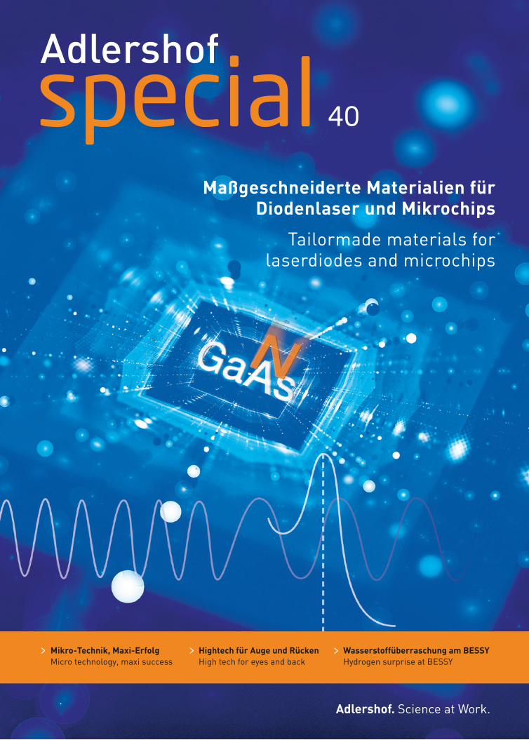
Tailormade materials for laserdiodes and microchips
13
40 Maßgeschneiderte Materialien für Diodenlaser und Mikrochips Tailormade materials for laserdiodes and microchips > Mikro-Technik, Maxi-Erfolg Micro technology, maxi success > Hightech für Auge und Rücken High tech for eyes and back > Wasserstoffüberraschung am BESSY Hydrogen surprise at BESSY
Transcript of Tailormade materials for laserdiodes and microchips
40
Maßgeschneiderte Materialien für Diodenlaser und Mikrochips
Tailormade materials for laserdiodes and microchips
> Mikro-Technik, Maxi-ErfolgMicro technology, maxi success
> Hightech für Auge und RückenHigh tech for eyes and back
> Wasserstoffüberraschung am BESSYHydrogen surprise at BESSY

3 Werkzeug der Zukunft Tool of the future
4 Schnell und präzise Fast and precise
8 Mikro-Technik, Maxi-Erfolg Micro technology, maxi success
10 Lasertechnik für den Weltmarkt Laser technology for the world market
12 Hightech für Auge und Rücken High tech for eyes and back
14 Sanft und sicher Gentle means safe
16 In neuem Licht: Laufsteg, Akademie und Mädchenkongress In a new light: Catwalk, Academy and girls congress
18 Die Milch unter der spektralen Lupe Milk under the spectral magnifying glass
20 Wasserstoffüberraschung am BESSY Hydrogen surprise at BESSY
23 Adlershof in Zahlen Adlershof in figures
Dr. Bernd LudwigLeiter Zentrum für Photonik und OptikTel.: +49 (0) 30 / 6392-2252Fax: +49 (0) 30 / 6392-2246E-Mail: [email protected] www.adlershof.de
Herausgeber // Publisher: WISTA-MANAGEMENT GMBH Redaktion // Editorial staff:Rico Bigelmann, Sylvia Nitschke
Autoren // Authors:Dr. Uta Deffke (ud), Mirko Heinemann (mh), Christian Hunziker (ch), Paul Janositz (pj), Chris Löwer (cl), Klaus Oberzig (ko), Peter Trechow (pt), Claudia Wessling (cw)
Übersetzung // Translation: Lost in Translation?, Endingen
Layout und Herstellung // Layout and production:Medienetage Anke Ziebell Telefon: 030/30 87 25 88, Fax: 030/97 00 54 81 E-Mail: [email protected]; www.ziebell-medienetage.de
Redaktionsadresse // Editorial staff address: WISTA-MANAGEMENT GMBH, Bereich Kommunikation Rudower Chaussee 17, 12489 Berlin Telefon: 030/63 92 - 22 38, Fax: 030 / 63 92 - 22 36 E-Mail: [email protected]; www.adlershof.de/special Anzeigenverkauf // Ad sales: WISTA-MANAGEMENT GMBH, Bereich Kommunikation Marina Salmon, Telefon: 030 / 6392-2283 E-Mail: [email protected]
Druck // Print: BGZ Druckzentrum GmbHwww.bgz-druckzentrum.de
© Fotos // © Photos:Sofern nicht anders gekennzeichnet/unless otherwise specied: Tina Merkau; Titel/Title: alexovicsattila – Thinkstock/Montage; S./p. 2: (Mitte/center) Photonic Tools, (oben/top) Dan Brandenburg – iStock; S./p. 3: Spectaris; S./p. 4/5: briddy – Thinkstock/iStock; S./p. 6: FBH/schurian.com; S./p. 7: Kristina Greke – iStock; S./p. 12: Fraunhofer IPK/IZM; S./p. 13: Ellex Deutschland GmbH; S./p. 14+15: (unten/bottom) DGZfP; S./p. 15: (oben/top) Jason Reed – Thinkstock/Photodisc; S./p. 16: TU Berlin; S./p.17: FBH; S./p. 18: Igor Tarasyuk–Thinkstock; S./p. 19: JTL Bio Tec.Analytics; S./p. 20/21: TU Wien; S./p. 22: Kevin Fuchs, www.kevinfuchs.com/my-beamline
Nachdruck von Beiträgen mit Quellenangabe gestattet. Belegexemplare erbeten. // Contributions indicated by name do not necessarily represent the opinion of the editorial staff. Reprinting of contributions permitted with source references. Specimen copies requested.
2015
www.adlershof.de/special
IMPRINT // IMPRESSUMINHALT // CONTENT
Ausführliche Texte und Adlershofer Termine finden Sie unter:
Die Photonik hat sich als Schlüsseltechnologie fürinnovative Hightech-Produkte in Anwendungsfeldern wieder Materialverarbeitung, der Medizintechnik und deroptischen Datenkommunikation fest etabliert. Diese inder Öffentlichkeit kaum wahrgenommene Dynamik derPhotonik-Branche will der Industrieverband SPECTARIS inZusammenarbeit mit Partnern besser bekannt machen.Das diesjährige Internationale Jahr des Lichts, das auch inAdlershof von zahlreichen Aktivitäten begleitet wird,eignet sich dazu besonders gut. Gemeinsam mit demOptecNet Deutschland e.V. werden wir aus diesem Anlassauch ein Buch mit Infografiken zur Photonik heraus-bringen,welchesdietechnischenAnwendungendesLichtsunddessenBedeutungfürunserheutigesLebenfür jeder-mannillustriert.
OptecNet, we shall be taking this occasion to issue a book with infographics on photonics that is to illustrate the technical applications of light and its importance in all our everyday lives.
Some interesting applications of light as a “tool of the future” can also be seen in the field of spectrometry. The progress of miniaturisation is giving rise to a huge new potential for spectroscopy: Today, spectrometry drones can measure the irrigation levels of agricultural fields, spectrometers in the form of smartphone addons are used by large scale campaigns for measuring air pollution in the Netherlands, and soon customers can also activate combinations of smartphone and spectrometer to measure directly the ripeness of fruit in supermarkets.
specialAdlershof
40
Wenko Süptitz, Leiter Fachverband Photonik, Industrieverband SPECTARIS
Wenko Süptitz, Photonics Association Director of the SPECTARIS Industry Association
Dipl.-Ing. Jörg Israel Leiter Zentrum für Mikrosysteme und MaterialienPhone: +49 (0) 30 / 63 92 - 22 16 Fax: +49 (0) 30 / 63 92 - 22 35 E-mail: israel(at)wista.dewww.adlershof.de
Ihre Ansprechpartner Your contact persons
WISTA-MANAGEMENT GMBH
Werkzeug der Zukunft Tool of the future
The success of photonics is based on developments along the entire value adding chain – from engineering glasses and semiconductors to complete optical systems. Here, the great success achieved by Adlershof institutes and compa-nies is specifically evident in the basic technologies as well. Some examples are nitride semiconductors developed for UV LEDs at the Leibniz Institute for Crystal Growth (IKZ) and the associated applications in medicine and the life sciences.
Over the long term, we see encouraging prospects of growth for German photonics companies. This is supported by all economic indicators for 2015, that the course will lead back to a long term growth trend and the 44 billion euro target predicted by the photonics sector report “Branchenreport Photonik” will be reached by 2020.
Interessante Anwendungen des Lichts als „Werkzeug derZukunft“zeigensichunteranderemimBereichderSpektro-meter.MitdemVoranschreitenderMiniaturisierungbietensich zahlreiche neue Möglichkeiten für die Spektroskopie:Spektrometer-Drohnen können heute den Stand der Be-wässerungvonFelderninderLandwirtschaftmessen,groß-angelegte Kampagnen zur Messung der Luftverschmut-zung in den Niederlanden nutzen SpektrometeraufsätzeanSmartphonesundauchderReifegradvonObstlässtsichmithilfe von Smartphone-Spektrometer-KombinationenschonbaldvonKundendirektimSupermarktmessen.
DerErfolgderPhotonikberuhtaufEntwicklungenentlangder gesamten Wertschöpfungskette – von technischenGläsern und Halbleitern bis hin zu kompletten optischenSystemen. Adlershofer Institute und Unternehmen sindhierbei insbesondere auch bei den Basistechnologien sehrerfolgreich. Die Entwicklung von Nitrid-Halbleitern imLeibniz-Institut für Kristallzüchtung zum Aufbau vonUV-LEDs und darauf aufbauende Anwendungen in derMedizin und im Life-Science-Bereich seien hier beispiel-gebendgenannt.
Langfristig sehen wir gute Wachstumsaussichten für diedeutschen Photonik-Unternehmen. Für 2015 sprechen alleKonjunkturindikatoren dafür, dass der Pfad zurück zumlangfristigenTrendwachstum führt und die im „Branchen-report Photonik“ prognostizierte Zielmarke von 44 Milliar-denEurobis2020erreichtwerdenkann.
Photonics has become permanently established as a key technology for innovative high tech products in fields like materials processing, medical engineering, and optical data communications. Scarcely entering the public eye, this dynamic development in the photonics sector is the focus of the industry association SPECTARIS, which, supported by partners, is attempting to give this a greater public aware-ness. This year’s International Year of Light, which will also be supported in Adlershof with a wide range of activi-ties, will provide the ideal platform for this. Together with
Adlershof special 40 3

Fast and preciseSchnell und präzise
Innovative Diodenlaser und Leuchtdioden eröffnen dem Maschinenbau,
der Medizintechnik und weiteren Feldern neue Anwendungsmöglich-
keiten. In Adlershof wird an der Zukunft dieser Technologie geforscht.
> weiter auf Seite 6
> read more on page 7
Innovative diode lasers and LEDs are tapping into new potential for
machine building, medical engineering, and other applications – and
soon direct lasers will be machining materials. Adlershof is researching
into the future of this technology.
Adlershof special 40 4 Adlershof special 40 5

Since the nineties, laser and LED technology has been inconceivable without gallium nitride (GaN). This chemical substance provides the basis for white LEDs and the blue diode lasers, e.g. in Blu-Ray players. Yet this does not even touch the extent of their true potential: The Ferdinand-Braun-Institut, Leibniz-Institut für Höchstfre-quenztechnik (FBH) has set itself the target of expanding this range of applications.
The research projects pursued at the FBH include the asso-ciation project “Advanced UV for Life”, involving 31 partners from industry and science. The object is to develop ultraviolet LEDs and their applications. “Conventional UV lamps based on mercury are unsuitable for many applications,” explained Sven Einfeldt from the FBH Business Unit for GaN Optoelec-tronics. For example, these conventional laser sources do not allow specific UV wavelength configurations – unlike diodes of gallium and aluminium nitride.
The challenge: “Mixed crystals of this kind are difficult to manufacture,” confided Einfeldt. “There is no substrate that allows the perfect growth of gallium or aluminium nitride crystals.” Yet this perfect growth is essential for the successful use of UV LEDs. Potential uses are manifold: therapy for skin diseases, for instance, the environmental and life sciences, the disinfection of drinking water, or the treatment of lacquers and paints.
Also the company DirectPhotonics, set up in 2011, has its eye on practical applications. Its specialised field deals with innovative, high performance diode lasers that are ideal for cutting and welding metal and for 3D production.
Seit den 1990er-Jahren ist Galliumnitrid (GaN) ausder Laser- und Leuchtdiodentechnologie nicht mehr weg-zudenken.DerHalbleiter ist Grundlage für weiße Leucht-dioden oder die blauen Diodenlaser, die beispielsweise inBlue-ray-Playern eingesetzt werden. Doch damit ist das
Anwendungsgebiet bei Weitem nichtausgeschöpft:DasFerdinand-Braun-
Institut, Leibniz-Institut fürHöchstfrequenztechnik (FBH),hat sich zum Ziel gesetzt, diePalette der Anwendungen zuerweitern.
ZudenForschungsvorhaben,die das Institut bearbei-
tet, gehört das Verbundpro-jekt „Advanced UV for Life“, an
dem 31 Partner aus Industrie undWissenschaft beteiligt sind. Ziel ist es,
ultraviolette Leuchtdioden (LED) zu verbessern und diePalette der Anwendungen zu erweitern. „HerkömmlicheUV-Lampen auf der Basis von Quecksilber sind für vieleAnwendungen nicht geeignet“, erläutert Sven Einfeldtvom Geschäftsbereich GaN-Optoelektronik des FBH. Beidiesen herkömmlichen Strahlern kann beispielsweise dieUV-Wellenlänge nicht genau eingestellt werden – andersalsbeiDiodenausGallium-undAluminiumnitrid.
Die Herausforderung: „Solche Mischkristalle sind schwie-rig herzustellen“, sagt Einfeldt, „denn es gibt kein Subs-trat, das es ermöglicht, Kristalle aus Gallium- oder Alu-miniumnitrid perfekt aufzubauen.“ Dies ist aber dieVoraussetzung dafür, UV-LEDs erfolgreich einzuset-zen. Möglichkeiten für den Einsatz gibt es viele:zur Therapie von Hautkrankheiten beispiels-weise, in den Bereichen Umwelt und LifeSciences, bei der Desinfektion von Trink-wasser sowie bei der Härtung vonLackenundFarben.
“You could say we’re selling the optical engine for machine building,” explained founder and Managing Director Wolf-gang Gries. “For this purpose, we combine semiconductors in such a way that they exhibit a particularly high beam performance.”
Just recently, DirectPhotonics developed initial products that were tested in an industrial environment. This year should see their launch. The extremely precise and reliable diode lasers, for example, allow innovative designs in the automo-tive industry and computer production. Gries is convinced: “This business field has a future. What makes this laser tech-nology so appealing is its automation level, its enhanced precision, and hence its essential contribution to the flexi-bility of industrial production.” In his view, the advantage of Adlershof lies in its basic research.
Das Attraktive an der Lasertech-nologie ist, dass sie einen hohen Automatisierungsgrad und eine
gesteigerte Präzision ermöglicht.
This business field has a future. What makes this laser technology so appealing is its automation level, its enhanced precision, and hence its essen-tial contribution to the flexibility
of industrial production.
Zwei-Zoll-Wafer mit Leuchtdioden
2-inch wafer with laser diodes
Oben links: UV-Leuchtdiode im Gehäuse
Top left: UV light emittin diode in its shell
DiepraktischeAnwendunghatauchdas2011gegründeteUnternehmen DirectPhotonics im Blick. Dessen Spezial-gebiet sind innovative Hochleistungsdiodenlaser, die ins-besondere für das Schneiden und Schweißen von Metallsowie für die 3D-Produktion geeignet sind. „Wir verkau-fen quasi den optischen Motor für den Maschinenbau“,erläutert Unternehmensgründer und GeschäftsführerWolfgang Gries. „Zu diesem Zweck kombinieren wirHalbleiterlaser so, dass sie eine besonders hohe Strahlen-performanceaufweisen.“
Seit kurzem sind erste Produkte aus dem HauseDirectPhotonics industriell getestet; im Lauf dieses Jahreswerden sie dem Markt zurVerfügung stehen. Die äußerstpräzisen und zuverlässigen Diodenlaser ermöglichen esbeispielsweise, in der Automobilindustrie oder in derComputerproduktioninnovativeDesignsumzusetzen.
DiesesGeschäftsfeldhatZukunft,istGriesüberzeugt:„DasAttraktive an der Lasertechnologie ist, dass
sie einen hohen Automatisierungsgradund eine gesteigerte Präzision ermög-
licht.“ Dabei bietet Adlershof nachAnsicht von Gries den Vorteil,dass hier Grundlagenforschungbetriebenwird. ch
Adlershof special 40 7Adlershof special 406

Die Technik ist in dieser Form einmalig und keines-wegs schnell erklärt. Dennoch gelingt Björn Wedel einanschaulicher Vergleich: „Im Grunde handelt es sichum ein Stromkabel mit Bohrmaschine – nur mit demUnterschied, dass kein Strom, sondern Laserlicht präzisezum bearbeitenden Werkstück geführt wird.“ Wedel istzusammenmitBernhardLummerGründerundGeschäfts-führer der PT Photonics Tools GmbH. Die vor knappzwei Jahren gegründete Firma entwickelt, produziert undvertreibt spezielle Laserwerkzeuge, mit denen Ultrakurz-pulslaser für viele Anwendungsgebiete industrietauglichwerden.
DieinnovativenSystemkomponentenfürUltrakurzpulslaser(UKP) ermöglichen es, dass der Laserstrahl ohne nennens-werte Leistungsverluste auf das Werkstück geführt unddort hochpräzise platziert wird. „Wir haben hier in Adlers-hof die Machbarkeit dieserTechnologie demonstriert, was
Innovative Unternehmen lassen Adlershof zu einem Hot Spot für Mikrooptik und Mikro-
systemtechnik werden. Ihr Wachstum und ihre Produkte überzeugen weltweit.
Mikro-Technik, Maxi-Erfolg
denEinsatzdesUKP indennächstenJahrenentscheidendbeeinflussenwird“,sagtWedel.DasAnwendungsspektrumin der industriellen Mikrobearbeitung wird sich drastischausweiten:vonderAutomobil-überdieHalbleiter-biszurElektronikbranche.SiealleprofitierenvondenVorteilendesUKP, durch die unterschiedliche Materialien – auch Kunst-stoffeundKohlefaserverbundwerkstoffe–flexibelmitdenhochenergetischen, extrem kurz gepulsten Laserstrahlenbearbeitet werden können. Dabei gelangt praktisch keineWärme in das Grundmaterial, wodurch sich der UKP-Laserhervorragend für die Oberflächenbearbeitung, etwa vonMikrochipsoderGlasfasern,eignet.
„EshandeltsichnichtumeinetechnischeSpielerei,sondernum eine Anwendung mit großem Marktpotenzial“, betontWedel. Entsprechend optimistisch blickt er in die Zukunft:Das jetzt15MitarbeiterstarkeStart-upsoll infünf Jahrenauf30bis50Beschäftigtewachsen. „Die InfrastrukturamStandortAdlershofunddiegutenRekrutierungsmöglichkei-tenunterstützendenweiterenAusbaudesUnternehmens“,sagtWedel.
AmbitionierteWachstumspläneverfolgtauchdieeagleyardPhotonicsGmbH,einführenderAnbietervonHochleistungs-laserdioden. Das 32-Mitarbeiter-Unternehmen möchte, soGeschäftsführerJörgMuchametow,denheutigenUmsatzvonfünfMillionenEuroinfünfJahrenverdoppelnunddasTeam um zehn neue Kräfte aufstocken. „Die Rekrutierungfällt leicht,daesdankderzahlreichenForschungsinstituteund den Unis in Berlin viele Spezialisten in dem Bereich Developed by PT Photonic Tools, the technology is unique
in this form and defies any cursory explanation. Björn Wedel nevertheless manages to give an understandable compar-ison: “Basically, it’s a power cable with integrated drilling machine. The only difference is that the cable doesn’t con-duct electricity, but laser light precisely to the machined workpiece.” Together with Bernhard Lummer, he is the co-founder and co-Managing Director of PT Photonic Tools GmbH. Set up less than two years ago, this company develops, produces, and markets special laser tools that make ultra short pulse lasers suitable for many industrial applications.
The innovative system components for ultra short pulse lasers guide the laser beam without appreciable power losses to the workpiece where they are applied to great pre-cision. “Here in Adlershof we have demonstrated the feasi-bility of this technology, and this will have a decisive effect on the uses of this laser type over the next few years,” said Wedel. The range of applications in industrial micromachin-ing will expand dramatically – in the automotive, semicon-ductor, and electronics sectors. They all can now benefit from the advantages of ultra short, high energy pulse lasers that can process flexibly a wide range of materials, including plastics and carbon fibre composites. In doing so, they trans-fer virtually no heat to the workpiece, making them ideal for the surfaces e.g. of microchips or glass fibres.
“This isn’t an application for techies, but one with great market potential,” stressed Wedel. Also his optimism about
the future reflects this view: the initial fifteen employees at the startup will grow to thirty to fifty in the next five years. “The growth of our company is supported further by the Adlershof infrastructure and the good recruiting potential here,” said Wedel.
Also eagleyard Photonics, a leading provider of high perfor-mance laser diodes, is pursuing ambitious plans for growth. CEO Jörg Muchametow is optimistic: employing 32, his com-pany intends to double its present five million euro turnover in just five years and add ten new workers to its team. “Re-cruitment is easy because the countless research institutes and the universities in Berlin have many specialists in this field,” said Muchametow. No bigger than a grain of rice, laser diodes are sold all over the world by his Adlershof company, mostly to laser system manufacturers and research insti-tutes. Their primary applications are in medical engineering, noncontacting instrumentation, spectroscopy, and space technology. The semiconductor technology eagleyard uses was developed at the Ferdinand-Braun-Institut, Leibniz- Institut für Höchstfrequenztechnik (FBH). “The FBH continues to be our most important cooperation partner and supplier of semiconductor chips,” said Muchametow. His view of Adlershof and its “active research community” as a hot spot for microoptics also finds testimony in the companies that have made their home here, like Jenoptik Diode Lab, Corning Optical Communications, DirectPhotonic Industries, OpTricon, C2GO inprocess solutions, and AEMtec.
Innovative companies are transforming Adlershof into a hot spot for microoptics and micro-
systems engineering. Their growth and their products have met with international acclaim.
Micro technology, maxi success
gibt“, sagt Muchametow. Die reiskorngroßen Laserdiodenwerden von Adlershof aus in alle Welt verkauft, meist anLasersystemhersteller und Forschungsinstitute. Hauptan-wendungsfelder sind die Medizintechnik, die berührungs-lose Messtechnik, die Spektroskopie und die Weltraum-technik. Die von eagleyard verwendete Halbleitertech-nologie wurde am Ferdinand-Braun-Institut, Leibniz-Institut für Höchstfrequenztechnik (FBH) entwickelt. „DasInstitut ist weiterhin unser wichtigster Kooperationspart-nerundZuliefererderHalbleiter-Chips“,sagtMuchametow.WieerüberhauptAdlershofmitseiner„aktivenForschungs-community“ als „Hot Spot“ für Mikrooptik betrachtet,was sich auch an den hier siedelnden Unternehmen wieJenoptik Diode Lab, Corning Optical Communications,DirectPhotonic Industries, OpTricon, C2GO inprocesssolutionsundAEMteczeige. cl
Hochleistungsdiodenlaser von eagleyard
High Power Laser diodes by eagleyard
Optischer Messaufbau zur Visualisierung von Strahlverlauf und Strahlübertragung
Optical meassuring setup visualising course and transfer of a beam
Untersuchung des Strahlprofils
Investigation of a beamprofile
Adlershof special 40 8 Adlershof special 40 9

EinesdieserProdukteisteinScanner,derdieQualitätvon Lebensmitteln untersuchen kann und speziell auf denchinesischenMarktzugeschnittenist.„InChinagibteseinstarkes Bedürfnis nach unabhängigen Lebensmittelkon-trollen“,erklärtXiaozhuoWang,derdieBrillianceFabBerlinGmbHleitet.HintergrundistderchinesischeLebensmittel-skandal von 2008. Damals wurde öffentlich, dass Milch-pulver jahrelang mit dem Kunstharzgrundstoff Melamingestreckt worden war. Kleinkinder hatten Nierenversagenerlitten.2010wareninChinaerneutmelaminhaltigeMilch-produkteentdecktworden.
Die Scanner sollen etwa so groß sein wie eine Espresso-maschine. „Denkbar ist, dass sie im Lebensmittelladenstehen. Dort kann jeder Kunde die Milchpulverpaketescannen und die Produkte auf Unbedenklichkeit prüfen
Das Potenzial ist riesig: Um auf deutscher Lasertechnologie basierende Produkte zu entwickeln, hat sich das Adlershofer Ferdinand-Braun-Institut, Leibniz-Institut für Höchstfrequenztechnik (FBH) mit dem chinesischen Unternehmen Sino Nitride Semiconductor (SNS) zusammengetan. Gemeinsam haben beide 2013 in Adlershof die Brilliance Fab Berlin GmbH (BFB) gegründet. Ihr Ziel: Die vom FBH entwickelten, Lasermodule sollen in Produkten überall auf dem Weltmarkt zur Anwendung kommen.
Lasertechnik für den Weltmarkt
The potential is enormous: With a view to developing products based on German laser technology, the Adlershof Ferdinand-Braun-Institut, Leibniz-Institut für Höchstfrequenztechnik (FBH) has pooled its resources with the Chinese company Sino Nitride Semiconductor (SNS). Together, the two founded in 2013 Brilliance Fab Berlin GmbH (BFB) that likewise is located in Adlershof. Its goal: the compact laser modules developed by FBH are to be used in products for the world market.
Laser technology for the world market
lassen“, so Wang. Die Konstruktion der Scanner erfolgtauf Basis der Raman-Spektroskopie. Dabei wird das zuuntersuchende Produkt mit Laserlicht bestrahlt. DasSpektrum des von der Probe gestreuten Lichts zeigt diegenaueZusammensetzungderSubstanz.„IstdarinMelaminenthalten, schlägt das Gerät Alarm“, so Wang. Die Laser-technikdafürstammtausdemFBH.
Für den Einsatz auf dem globalen Automobilmarkt ent-wickeltBFBLasermodulezurBeleuchtung.DieerstenAuto-mobilemitLaser-ScheinwerfernvonBMWkommenbereitsauf den Markt. „LED-Scheinwerfer haben eine Reichweitevonmaximal300Metern.AufLaserbasierendeScheinwer-fer schaffen bis zu 600 Meter“, sagt Wang. Es gibt bereitseinAbkommenmiteinemchinesischenAutozuliefererüberdieProduktionvonRücklichtern.EinweiteresFeldsindBild-schirmemitmehralszweiMeternDurchmesser.„VorallembeigroßenDisplayseignetsichdieLasertechnologiebesseralsLED“,erläutertWang.„Mankannüber30ProzentEnergieeinsparen.“
Xiaozhuo Wang kennt die Bedürfnisse des chinesischenMarktes gut, schließlich ist er in Changchun aufgewach-sen, der alten Hauptstadt der Mandschurei. Die deutscheSprache lernteervor15 Jahren inderLutherstadtWitten-berg. Später studierte er Elektrotechnik in Bochum undlerntedasFBHbeieinemPraktikumkennen,woerschließ-lich promovierte – natürlich über Laser. Der Impuls zurGründungdesUnternehmensBFBkamvonProfessorZhangGuoyi, der an der Peking Universität lehrt und außerdemdieGeschäftedeschinesischenUnternehmensSinoNitrideSemiconductor(SNS)führt.
„Das FBH ist eine Institution“, sagt Wang beinahe ehr-fürchtig. „Es ist wunderbar hier zu sein, nur wenigeMinutenFußwegentfernt. JedesThemakannmanschnelldiskutieren.“ mh
One of these products is a scanner that can analyse the quality of food and is designed specifically for the Chinese market. “China is badly in need of independent food control,” explained Xiaozhuo Wang, Director of this company. The background was provided by the Chinese food scandal of 2008. Then it was disclosed that powdered milk had been stretched for years with the synthetic resin base melamine, causing kidney failure in infants. In 2010, dairy products containing melamine again made the news in China.
The planned scanners are about as big as espresso ma-chines. “It’s conceivable that they’ll be available in grocery shops. Customers can then scan the powered milk packets and check them for any health hazards,” explained Wang. The principle behind these scanners is based on so called Raman spectroscopy. This involves irradiating the analysed product with laser light whose scattered spectrum contains the exact composition of the sample. “The device sounds an alarm when it detects melamine,” said Wang. The laser technology was developed by the FBH.
BFB develops lighting laser modules for use on the global automotive market. BMW is already launching the first cars
with laser headlights. “LED headlights can reach 300 me-tres at most. For laser based headlights, this can be as high as 600 metres,” explained Wang. Even now, an agreement on the production of tail lights has been reached with a Chi-nese car parts supplier. A further field is the production of displays over two metres in diameter. “Above all large dis-plays operate better with laser technology than with LEDs,” said Wang. “And the energy savings are over 30 percent.”
Xiaozhuo Wang is well familiar with the needs of the Chinese market. After all, he grew up in Changchun, the one-time capital of Manchuria. He learned German fifteen years ago in Lutherstadt Wittenberg. Studying electronic engineering in Bochum, he learned about the FBH during a period of practical training. At this institute he was also awarded his doctorate, not surprisingly in lasers. The idea of setting up the BFB company came from Profes-sor Zhang Guoyi, who was teaching at Peking University and also managing the business of the Chinese company Sino Nitride Semiconductor (SNS).
“The FBH is an institution,” said Wang, almost in awe. “It’s great to be here, only a few minutes’ walk away. Any subject can be brought up quickly for discussion.”
Beim Drahtbonding werden mittels dünner Drähte Anschlüsse zum Beispiel von Leucht- oder Photodioden mit den elektrischen Anschlüssen des Chipgehäuses verbunden.
When wire bonding connections of photodiodes or light emitting diodes are bonded with the electrical connections of the chip package using thin wires.
Xiaozhuo Wang, Gründer von BFB Xiaozhuo Wang, founder of BFB
Adlershof special 40 11Adlershof special 40 10

“Today, more than 20,000 Ellex lasers and ultrasonic devices are being used in the treatment of eye diseases,” said Bernhard Lobmayr. This economist is the manager of Ellex Deutschland GmbH, which moved into the Adlershof Photonics and Optics Centre (ZPO) in 2014. At present, seven employees are responsible for sales and services. Lobmayr is confident: soon, they could be assuming more responsibili-ties, for instance in the development of products and thera-pies.
Its short pulse lasers have launched Ellex to the world lead-ership in the treatment of glaucoma and (successive) cata-racts. The company has proved particularly innovative in its fight against age related macular degeneration. “In recent years, retinal treatment has benefited greatly from the minimally invasive laser therapy 2RT, or retinal rejuvenation therapy,” explained Lobmayr. Here, extremely short light pulses induced the healing process without injuring the retinal sensors.
The Berlin Fraunhofer Institute for Reliability and Micro- integration (IZM) researches into the prevention of back complaints. This developed the “intelligent” jacket
Hightech für Auge und Rücken
Hightech for eyes and back
Mit kurz gepulsten Lasern ist Ellex weltweit führend beider Behandlung des Glaukoms und des Grauen Stars(Nachstar).BesondersinnovativzeigtsichdieFirmabeiderBekämpfung der altersbedingten Makuladegeneration, beider es zum Nachlassen der zentralen Sehschärfe kommt.„Für die Behandlung der Netzhaut wurde in den letztenJahren die minimal invasive Lasertherapie 2RT (retinaleRegenerationstherapie) entwickelt“, sagt Lobmayr. ExtremkurzeLichtpulsesetzendenHeilungsprozessinGang,ohnedieSensorikderNetzhautzuverletzen.
Mit derVerhinderung von Rückenbeschwerden beschäftigtsichdasBerlinerFraunhofer-InstitutfürZuverlässigkeitundMikrointegration(IZM).Dortwurdedie„intelligente“Weste„CareJack“ entwickelt. In dem vom Bundesforschungs-ministeriumgefördertenProjektgehtesdarum,PflegekräftebeikörperlichschwerenTätigkeitenzuunterstützenundsovor Rückenleiden zu bewahren. Eine mit modernerTechnikgespickte Orthese – leicht, flexibel und bequem – bietetgezielte Kraftunterstützung und stabilisiert den Rücken.ZudemwarnenSignalevorfalschenBewegungen.
AmProjektsindachtPartnerbeteiligt.SiekommenausderIndustrie, aus Kliniken, der Rehabilitation und Pflege. Auchzwei Berliner Fraunhofer-Institute (FHI) gehören dazu, dasIPK(FHIfürProduktionsanlagenundKonstruktionstechnik)unddasIZM.DortwurdedieSchaltungentworfenundnachoptimalerIntegrationvonSensorenundpräziserSteuerungvonAktorengesucht.
„Wichtig sind die Robustheit der Datenerfassung undwiderstandsfähige elektronischeVernetzung, da dieWestewienormaleKlinikkleidunggereinigtwerdensoll“,sagtUlfOestermannvomIZM.DieeinzelnenSystemewieminiatu-risierte Aktoren, flexible Leiterplatten und Sensoren sollennoch 2015 zu einem Prototyp zusammengefügt werden.DannstehtderPraxistestan,bevorvoraussichtlichineinbiszweiJahrendieSerienfertigungstartenkann. pj
“CareJack”, a project sponsored by the German Federal Ministry of Research to assist nursing staff in physically demanding activities, thereby minimising the risk of back complaints. An orthopaedic device bristling with modern technology – light, flexible, and convenient – supports muscular activities where needed and stabilises the back. Also, it emits alarms when it detects wrong movements.
Involved in the project are eight partners from industry, clinics, rehabilitation, and nursing care. These also include two Berlin Fraunhofer Institutes (FHI), the IPK for production systems and design technology and the IZM. These designed the circuitry and researched into the optimal integration of sensors and the precise control of actuators.
“The jacket must be cleaned like normal clinical clothing, so great importance was attached to robust data capture and stable electronic networking,” explained Ulf Oestermann of the IZM. The plan is to assemble each of the systems like miniaturised actuators, flexible PCBs, and sensors into a prototype as early as 2015. After that comes the field test and then series production, which is expected to be launched in one to two years.
„Heute werden mehr als 20.000 Ellex-Laser undUltraschallgeräte zur Behandlung von Augenerkrankungeneingesetzt“,sagtBernhardLobmayr.DerWirtschaftswissen-schaftler leitet die Ellex Deutschland GmbH, die seit 2014im Adlershofer Zentrum für Photonik und Optik zu Hauseist.DerzeitsiebenMitarbeitersindmitVerkaufundServicebeschäftigt. Bald könnten noch mehr Aufgaben dazu-kommen, etwa die Entwicklung von Produkten undThera-pieverfahren,sagtLobmayr. Wheretheeyesareconcerned,thegreatestcautionisneeded,for
instanceinthetreatmentofglaucomathatgraduallyrestrictsthefieldofvision.Aboutoneintensuffererslosetheireyesight.Bydevelopinggentlemethods,thecompanyEllexfoundedinAustraliain1985hasevolvedintotheleaderinophthalmologictechnologies.AndtechnologiesdevelopedinAdlershofarealsotoaidinthetreatmentofbackcomplaints.
Die intelligente Weste „CareJack“
The intelligent jacket ”CareJack“
Mit kurz gepulsten Lasern ist Ellex bereits weltweit führend bei der Behand-
lung des Glaukoms und des Grauen Stars.
Its short pulse lasers have launched Ellex to the world leadership in the treatment of
glaucoma and (successive) cataracts.
WennesumdieAugengeht,istgrößteVorsichtangebracht.EtwabeimGlaukom(GrünerStar),beidemdasGesichtsfeldallmählicheingeschränktwird.RundjederzehnteErkrankteerblindet.MitderEntwicklungschonenderMethodenistdieFirmaEllex,1985inAustraliengegründet,zumTechnologieführerinderAugenheilkundegeworden.UndauchbeiderRückenvorsorgesollinAdlershofentwickelteTechnikhelfen.
Adlershof special 40 13Adlershof special 4012
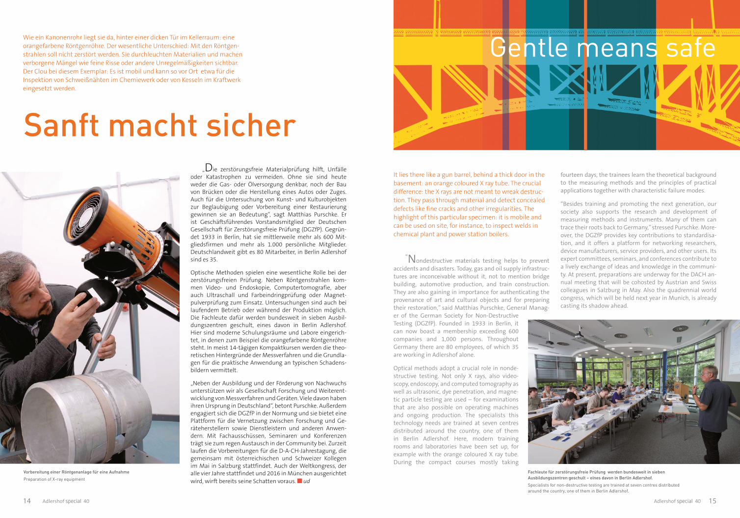
„Die zerstörungsfreie Materialprüfung hilft, Unfälleoder Katastrophen zu vermeiden. Ohne sie sind heuteweder die Gas- oder Ölversorgung denkbar, noch der Bauvon Brücken oder die Herstellung eines Autos oder Zuges.Auch für die Untersuchung von Kunst- und Kulturobjektenzur Beglaubigung oder Vorbereitung einer Restaurierunggewinnen sie an Bedeutung“, sagt Matthias Purschke. Erist Geschäftsführendes Vorstandsmitglied der DeutschenGesellschaftfürZerstörungsfreiePrüfung(DGZfP).Gegrün-det 1933 in Berlin, hat sie mittlerweile mehr als 600 Mit-gliedsfirmen und mehr als 1.000 persönliche Mitglieder.Deutschlandweitgibtes80Mitarbeiter,inBerlinAdlershofsindes35.
Optische Methoden spielen eine wesentliche Rolle bei derzerstörungsfreien Prüfung. Neben Röntgenstrahlen kom-men Video- und Endoskopie, Computertomografie, aberauch Ultraschall und Farbeindringprüfung oder Magnet-pulverprüfungzumEinsatz.Untersuchungensindauchbeilaufendem Betrieb oder während der Produktion möglich.Die Fachleute dafür werden bundesweit in sieben Ausbil-dungszentren geschult, eines davon in Berlin Adlershof.HiersindmoderneSchulungsräumeundLaboreeingerich-tet,indenenzumBeispieldieorangefarbeneRöntgenröhresteht.Inmeist14-tägigenKompaktkursenwerdendietheo-retischenHintergründederMessverfahrenunddieGrundla-genfürdiepraktischeAnwendungantypischenSchadens-bildernvermittelt.
„NebenderAusbildungundderFörderungvonNachwuchsunterstützenwiralsGesellschaftForschungundWeiterent-wicklungvonMessverfahrenundGeräten.VieledavonhabenihrenUrsprunginDeutschland“,betontPurschke.AußerdemengagiertsichdieDGZfPinderNormungundsiebieteteinePlattform für dieVernetzung zwischen Forschung und Ge-räteherstellern sowie Dienstleistern und anderen Anwen-dern. Mit Fachausschüssen, Seminaren und KonferenzenträgtsiezumregenAustauschinderCommunitybei.ZurzeitlaufendieVorbereitungenfürdieD-A-CH-Jahrestagung,diegemeinsam mit österreichischen und Schweizer KollegenimMai inSalzburgstattfindet.AuchderWeltkongress,derallevierJahrestattfindetund2016inMünchenausgerichtetwird,wirftbereitsseineSchattenvoraus. ud
Itliestherelikeagunbarrel,behindathickdoorinthebasement:anorangecolouredXraytube.Thecrucialdifference:theXraysarenotmeanttowreakdestruc-tion.Theypassthroughmaterialanddetectconcealeddefectslikefinecracksandotherirregularities.Thehighlightofthisparticularspecimen:itismobileandcanbeusedonsite,forinstance,toinspectweldsinchemicalplantandpowerstationboilers.
“Nondestructive materials testing helps to prevent
accidents and disasters. Today, gas and oil supply infrastruc-tures are inconceivable without it, not to mention bridge building, automotive production, and train construction. They are also gaining in importance for authenticating the provenance of art and cultural objects and for preparing their restoration,” said Matthias Purschke, General Manag-er of the German Society for Non-Destructive Testing (DGZfP). Founded in 1933 in Berlin, it can now boast a membership exceeding 600 companies and 1,000 persons. Throughout Germany there are 80 employees, of which 35 are working in Adlershof alone.
Optical methods adopt a crucial role in nonde-structive testing. Not only X rays, also video- scopy, endoscopy, and computed tomography as well as ultrasonic, dye penetration, and magne- tic particle testing are used – for examinations that are also possible on operating machines and ongoing production. The specialists this technology needs are trained at seven centres distributed around the country, one of them in Berlin Adlershof. Here, modern training rooms and laboratories have been set up, for example with the orange coloured X ray tube. During the compact courses mostly taking
WieeinKanonenrohrliegtsieda,hintereinerdickenTürimKellerraum:eineorangefarbeneRöntgenröhre.DerwesentlicheUnterschied:MitdenRöntgen-strahlensollnichtzerstörtwerden.SiedurchleuchtenMaterialienundmachenverborgeneMängelwiefeineRisseoderandereUnregelmäßigkeitensichtbar.DerCloubeidiesemExemplar:EsistmobilundkannsovorOrtetwafürdieInspektionvonSchweißnähtenimChemiewerkodervonKesselnimKraftwerkeingesetztwerden.
Sanft macht sicherfourteen days, the trainees learn the theoretical background to the measuring methods and the principles of practical applications together with characteristic failure modes.
“Besides training and promoting the next generation, our society also supports the research and development of measuring methods and instruments. Many of them can trace their roots back to Germany,” stressed Purschke. More-over, the DGZfP provides key contributions to standardisa-tion, and it offers a platform for networking researchers, device manufacturers, service providers, and other users. Its expert committees, seminars, and conferences contribute to a lively exchange of ideas and knowledge in the communi-ty. At present, preparations are underway for the DACH an-nual meeting that will be cohosted by Austrian and Swiss colleagues in Salzburg in May. Also the quadrennial world congress, which will be held next year in Munich, is already casting its shadow ahead.
Gentle means safe
Fachleute für zerstörungsfreie Prüfung werden bundesweit in sieben Ausbildungszentren geschult – eines davon in Berlin Adlershof.
Specialists for non-destructive testing are trained at seven centres distributed around the country, one of them in Berlin Adlershof.
Vorbereitung einer Röntgenanlage für eine Aufnahme
Preparation of X-ray equipment
Adlershof special 40 14 Adlershof special 40 15

Passend zum Jahr des Lichts erinnerte die Sonnenfinsternis vom 20. März 2015 daran, dass es ohne Sonnenlicht kein Leben auf unserem Planeten geben würde. Nach Jahr-tausenden passiver Sonnenenergienutzung ist die moderne Wissenschaft zur aktiven Nutzung der optischen und photonischen Technologien übergegangen. Schon seit den 1960er-Jahren ist der Standort Adlershof an dieser Entwicklung führend beteiligt.
Well befitting the International Year of Light, the solar eclipse on 20 March 2015 was a reminder that without sunlight there would be no life on our planet. After millennia
of passive solar harvesting, modern science has moved to the active utilisation of optical and photonic technologies. As far back as the 1960s, Adlershof has been
adopting a leading position in this development.
Today, over half a dozen university and nonuniversi-ty institutes have been pressing ahead with their research activities. These have been joined by a good seventy high tech businesses that have been set up nearby to explore all the facets of light as a tool. Their objective this year is to cast a light on their growing importance in industrial developments, power supply systems, medicine, and consumer products.
Since early March, the German Museum of Technology has been presenting the “LED catwalk” on 1500 square metres, a paradigm shift that is currently progressing through the lighting sector. LEDs make variable lighting concepts pos-sible. They can be fitted with the most diverse optical sys-tems, switched in any configuration, dimmed, and colour programmed. They can be configured specifically for any lighting situation, whether on a rain drenched road or inside buildings or production halls. Additive manufacturing meth-ods are tapping into new product design potential, giving rise to unique geometries and contours, and all under the sign of maximum energy efficiency. Insights into this new world of unique lighting possibilities are presented, for in-stance, by the “LED plus 3D” workshop, whose organisation is shared by the optical technologies network OpTecBB. The goal was to bring together new possibilities in lighting engineering, product design, and 3D printing and to sound out the potential for innovation at this interface.
The central subject is not only lighting, but also high speed data transmission and processing. Held in mid March at the Heinrich Hertz Institute and also in Adlershof, the Photonics Academy targeted Masters students of engineering and natural sciences. Its message: big data and its transmission over fibre optics, i.e. by means of light, have now become inseparable.
These events stand as examples of a great many confe- rences, workshops, and competitions in Berlin that are drawing attention to the significance of optical technologies in the Year of Light. These target above all young persons. One highlight in October will be the 6th Girls Technology Congress that will be hosted under the title “GoPhoton! – Discover the power of light”. Supported in particular by the dedication of the Ferdinand-Braun-Institut, Leibniz-Institut für Höchstfrequenztechnik, this will also present the writing competition “LichtBlicke” where contestants can enter their poems, short stories, and essays on the subject of light. In line with the motto “Licht dichten oder rappen” (“Write or rap light”), the fifteen best contributions will be recited at a concert. The competition is open to secondary school pupils in Berlin and Brandenburg.
On 9–18 October, the Year of Light is to end on a worthy note with the Festival of Lights in Berlin. Yet this jubilee year is to be honoured inside the Adlershof science location as well: this year, Bernd Ludwig, Director of the Photonics/Optics Centre, will start replacing all energy saving lamps with LEDs.
IN NEUEM LICHT LAUFSTEG, AKADEMIE UND MÄDCHENKONGRESS
IN A NEW LIGHT CATWALK, ACADEMY AND GIRLS CONGRESS
Experimentieren auf dem Mädchen-Technik-Kongress
Experimenting at the convention ”Girls and technology“
Workshop zum Thema Lichtmalerei
Light painting workshop
Aktuell treiben ein Dutzend universitärer und außer-universitärer Institute die Forschung voran. Um sie herumhabensichgut70Hightechunternehmenangesiedelt,derenGeschäftsmodellesichumdasWerkzeugLichtinallenseinenFacetten drehen. Dass sie in der industriellen Entwicklung,der Energieversorgung, der Medizin oder den Konsumer-produkteneineimmerwichtigereRollespielen,giltesgeradeindiesemJahrinsrechteLichtzurücken.
SeitAnfangMärzdemonstriertder„LED-Laufsteg“amDeut-schen Technikmuseum auf 1.500 Metern den Paradigmen-wechsel,denderBeleuchtungsmarktaktuelldurchläuft.MitLeuchtdioden,denLEDs,sindvariableBeleuchtungskonzeptemöglich.SiekönnenmitunterschiedlichenOptikenbestückt,beliebiggeschaltet,gedimmtundfarbigvariiertwerden.Fürjede Beleuchtungssituation kann eine maßgeschneiderteKonfiguration ermittelt werden, ob auf regennasser Fahr-bahnoderinnerhalbvonGebäudenoderProduktionshallen.Additive Fertigungsverfahren eröffnen neue MöglichkeitenbeimProduktdesign,einzigartigeFormenundKonturenwer-denumsetzbarundallesunterdemSignumhöchsterEner-gieeffizienz.EinblickeindieseneueWeltder„uniquelightingpossibilities“ vermittelte zum Beispiel der Workshop „LEDplus 3D“, den das Kompetenznetz Optische TechnologienOptec-Berlin-Brandenburg (OpTecBB) e.V. mitorganisierte.Ziel war es, neue Möglichkeiten bei der Lichttechnik, beimProduktdesignundbeim3D-DruckzusammenzubringenundInnovationspotenzialeandieserSchnittstelleauszuloten.
Neben der Beleuchtung ist die Hochgeschwindigkeits-Datenübertragung und -verarbeitung zentrales Thema. Die
„Photonik-Akademie“, die Mitte März im Heinrich-Hertz-Institut und auch in Adlershof stattfand, richtete sich anMasterstudenten der Ingenieur- und Naturwissenschaf-ten. Big Data und deren Übertragung per Glasfaser – alsomit Licht, so die Botschaft, gehören inzwischen untrennbarzusammen.
DieseVeranstaltungenstehenexemplarischfüreineVielzahlvonKonferenzen,WorkshopsundWettbewerbeninBerlin,mitdenendieOptischenTechnologienimJahrdesLichtsaufihreBedeutungaufmerksammachen.VorallemdasInteressederJugendsollgewecktwerden.EinHighlightwirdimOktoberder6.Mädchen-Technik-KongressunterdemTitel„GoPhoton!–Discoverthepowerof light“sein,beidemsichbesondersdas Ferdinand-Braun-Institut, Leibniz-Institut für Höchst-frequenztechnik (FBH) engagiert. Für den dazugehörigenSchreibwettbewerb „LichtBlicke“ werden Gedichte, Kurz-geschichten, Essays zum Thema Licht gesucht. Nach demMotto „Licht dichten oder rappen“ werden die 15 bestenWettbewerbsbeiträge in einem Konzert aufgeführt. Teil-nehmenkönnenSchülerderSekundarstufeausBerlinerundBrandenburgerSchulen.
Einen würdigen Abschluss soll das Jahr des Lichts vom9.bis18.Oktober2015mitdem„FestivalofLights“inBerlinfinden. Aber auch innerhalb des WissenschaftsstandortesAdlershofsolldasJubeljahrgenutztwerden:BerndLudwig,Leiter des Zentrums für Photonik/Optik, beginnt in diesemJahr,alleEnergiesparlampeninseinemZentrumdurchLEDszuersetzen. ko
Adlershof special 40 17

DerlangeFlug,dasungenießbareLeitungswasserunddievielerortsmitMelaminundPalmfettgepanschteMilchhabenFrankWagnerbeiseinenReisennachIndiengarnichtgefallen.DochdieBesucheinAhmedabadimBundesstaatGujarathabensichausgezahlt:DasindischeUnternehmenEverest Instruments übernimmt künftig die Produktion ei-nesvonWagnerentwickeltenMessgerätsfürMilchfett.DieVertriebsrechte des FatScan genannten tragbaren Spek-trometers für Europa hat sich JTL laut Wagner allerdingsgesichert.„DieInderliefernunsdanndieGeräte“.
Vor etwa 20 Jahren begann der Aufstieg der Spektrosko-piebeiderAnalysevonProbenunterschiedlichsterArt.DieTechnikbasiertaufderWechselwirkungzwischenMaterieund elektromagnetischen Wellen. Unterschiedliche Stoffeabsorbieren oder emittieren Energie bei unterschiedlichenWellenlängen.Dasdaraus indenMessungenentstehendeInfrarot-SpektrumlässtoftpräziseRückschlüsseaufdieZu-sammensetzungeinerProbezu.
„EsgibtinunsererBrancheeinigePlatzhirsche,dieSpektro-meterfürmehrals10.000Euroanbieten“,sagtderPhysiker.SolcheGerätesteheningrößerenLabors,etwabeibehörd-lichen Lebensmittelkontrolleuren. Kleinere UnternehmenmüssenjedochinderRegelgarnichtsovieleParameterun-tersuchen,dasssichdieAnschaffunglohnt.Sieinteressierensich unter anderem für den Fettanteil, nach dem sich derPreis der Milch richtet. „Wir wollen mit abgespeckter Sen-sorik und kleineren Geräten niedrigpreisige Angebote ma-chen“,erläutertWagner.DermitkurzwelligerInfrarotstrah-lungarbeitendeFatScanvonJTLetwakostetzwischen1.000und1.500EuroundistfürdenLandwirtperKnopfdruckzubedienen.
GroßesPotenzialsiehtWagnerfürdieSpektralanalyseauchbeiderUntersuchungvonGranulatenimLebensmittel-undPharmabereich, bei denen geschaut wird, ob ein Wirkstoffrichtig eingeschlossen oder ob Feuchtigkeit vorhanden ist.Ganz verzichten wird die Lebensmittelanalytik nicht aufdas Nasslabor, denn viele Stoffe lassen sich mit Spektros-kopie allein nicht zweifelsfrei identifizieren. Laktose undHarnstoff etwa liefern in Spektralanalysen nur geringeSignale, manche Stoffe sind nur durch physikalischeMessung nicht zu unterscheiden. Manchmal sei der GanginsLabordochunverzichtbar. cw
Die Firma JTL-BioTec.Analytics aus Adlershof entwickelt und vermarktet Messtechnik für die Lebensmittel- und Medikamentenanalyse. Sie setzt auf preiswerte Hightech-Geräte, die sich auch kleinere Betriebe leisten können. Gefertigt wird bald auch in Indien.
Die Milch unter der spektralen Lupe
The company JTL-BioTec.Analytics of Adlershof develops and markets instrumentation for the analysis of food and medi-cines. It is proud of its low cost high tech that also smaller firms can afford. Production will soon be starting in India as well.
Milk under the spectral magnifying glass
There’s a good reason why milk is subject to stringent control. Inflamed udders can allow the passage of microbes that spoil the yogurt or cheese in subsequent production stages. Transported milk can be contaminated from soiled pipes. For this reason, also smaller dair-ies and agricultural holdings are interested in the tightest possible control procedures – and this market segment is the focus of Wagner’s company. “Our sector is home to a number of top dogs that offer spectrometers in excess of 10,000 euro,” said the physicist. These de-vices stand in major laboratories, for instance of government food inspectors. Smaller com-panies, on the other hand, generally do not
have to analyse so many parameters, so the purchase pays off. They are interested among other things in the fat con-tent, which defines the price of milk. “We want to offer low cost, smaller instruments with stripped down sensors,” explained Wagner. The FatScan from JTL operates with short wave infrared radiation, costs between 1,000 euro and 1,500 euro, and returns results at the simple push of a button.
Wagner also sees great potential for spectral analysis in food and pharmaceutical granulates. Here, his products can detect moisture and determine whether an agent has been encapsulated properly. Of course, food analyses will not completely do away with the wet chemistry labora- tory: spectroscopy alone cannot detect all substances with absolute certainty. Lactose and urea, for instance, cast only weak signals in spectral analyses, and a number of sub-stances cannot be differentiated between through physical measurements alone. Sometimes, the way through the laboratory is still indispensable.
Auch für die Untersuchung von Lebensmitteln auf Zu-sammensetzung und mögliche Schadstoffe ist Spektros-kopie mittlerweile unverzichtbar: „Von Vorteil ist, dass esschnellergehtalsbeidennasschemischenVerfahren,diezudenhäufigstenangewandtenMethodeninderanalytischenChemie gehören“, die wegen des nötigen Fachpersonalsauchteurerseien,sagtWagner.
JTLhatsichvorallemaufMilchundMilchproduktespeziali-siert.SiebietetnebenSpektrometernundOsmometernzurBestimmung von Masseverhältnissen und GefrierpunktenauchServiceundhilftdenKunden,diekompliziertenGerätezukalibrieren.
Milch wird aus gutem Grund ausgiebig kontrolliert: DurchEuterentzündungen können Keime hineingelangen, die infolgenden Produktionsstufen auch den Joghurt oder Käseverderben. Beim Transport könnte sie durch verschmutzteRohre kontaminiert werden. Auch kleinere Molkereien undLandwirtschaftsbetriebe sind deshalb an einer möglichstengmaschigen Kontrolle interessiert – auf dieses Markt-segmentzieltWagnersFirma.
On his travels to India, Frank Wagner has only bad memories of the long flight, the undrinkable mains water, and the ubiquitous milk laced with melamine and palm fat. Yet his visits to Ahmedabad in the state of Gujarat paid off: the Indian company Everest Instruments will be taking over the future production of an instrument that Wagner developed to measure milk fat. Wagner admitted, howev-er, that JTL had long secured the rights to sell the portable spectrometer, called the FatScan, in Europe – “the Indians then supply us with the instruments”.
Spectroscopy for the purpose of analysing all kinds of sam-ples began its rise about twenty years ago. The technology is based on the interaction between material and electro-magnetic radiation. Different substances absorb and emit energy at different wavelengths. The infrared spectrum captured by the measurements often allows precise con-clusions on the composition of a sample.
In the meantime, spectroscopy has become indispensable for analysing the composition and potential contaminants in food as well. Wagner is convinced: “The advantage is that it’s faster than wet chemical methods,” which are also more expensive because they need specialists.
JTL specialises above all in the analysis of milk and dairy products. Besides spectrometers and osmometers for quan-tifying mass ratios and freezing points, it also provides ser-vices and helps its customers to calibrate the complex in-struments.
Milch-Analysator FatScan von JTL JTL-device FatScan for analysis of milk
Adlershof special 40 18 Adlershof special 40 19

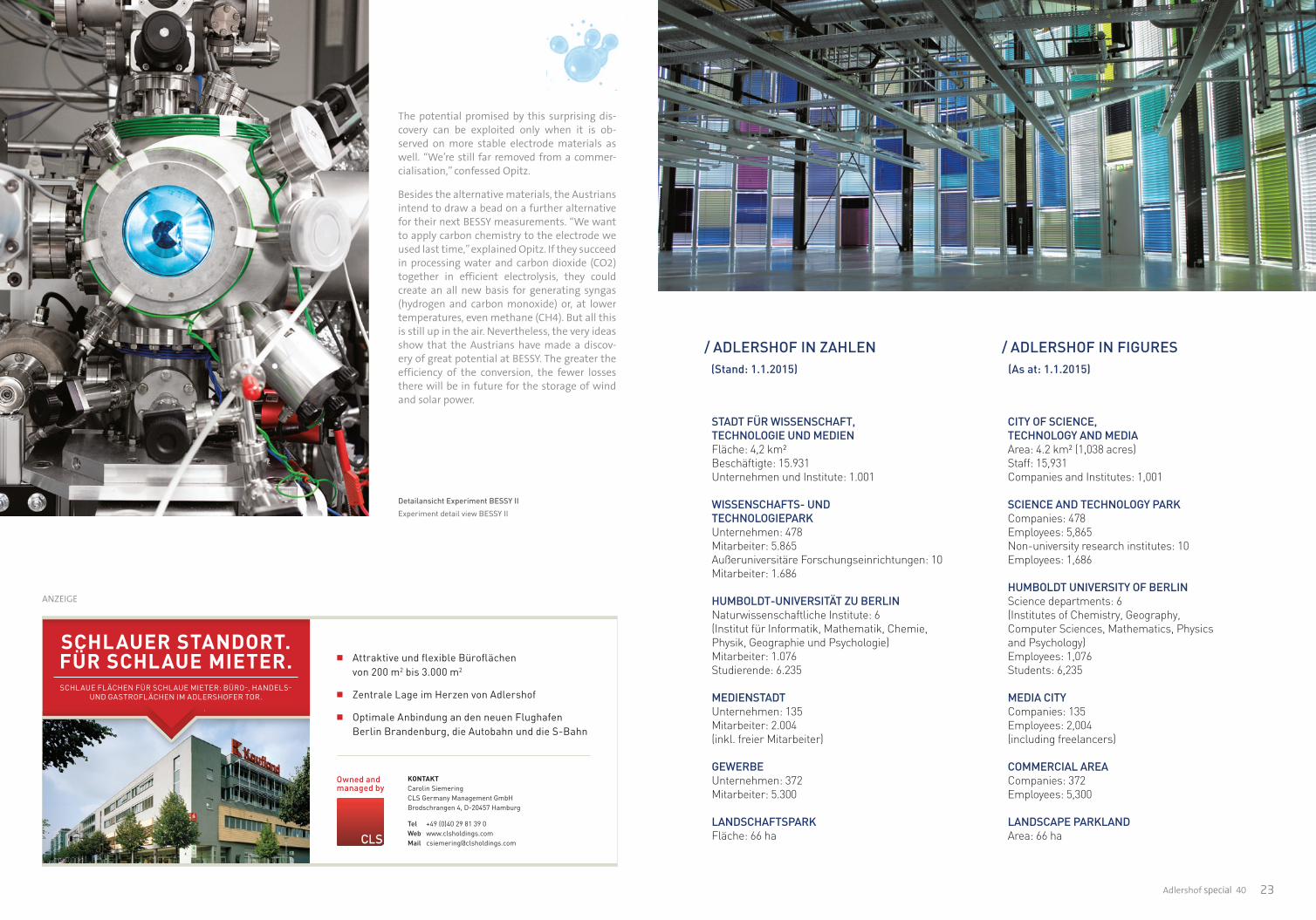
vorbereitete Perowskit-Elektroden inEchtzeit beim Elektrolyse-Prozessspektroskopischuntersucht.
„Uns ging es darum, den Einfluss derPolarisation auf die Bindungen ander Perowskit-Oberfläche genauer zuverstehen“, berichtet Opitz – typischeFragen der Grundlagenforschung.Plötzlich jedoch tauchte unter katho-discher Polarisation im Spektrumein neuer Peak auf. Klötzer erkanntesofort:HierwarEisenimSpiel!
Jeweils unter Spannung „schwitzte“der Perowskit das Metall aus undnahm es wieder auf, sobald keineSpannungmehranlag.DasBesondere:Mit Austreten des Metalls an dieElektroden-Oberfläche nahm die Elek-trolyse Fahrt auf. Die Menge des er-zeugtenWasserstoffsstiegrasant.
„Wir haben diesen Effekt als erstesTeamin-situbeobachtenkönnen–unddasvölligungeplant“,freutsichOpitz.Zwar war schon vorher bekannt, dassauf der Oberfläche von Perowskitenmetallische Partikel wachsen können.Doch der positive elektrokatalytischeEinflusswarneu.DieÖsterreicherha-ben nun eine weitere MesskampagneamBESSYbeantragt,umihreBeobach-tung auf verwandte Materialien zuübertragen. Denn der eingesetztePerwoskit ist zu instabil und zu we-nig leitfähig, als dass er im großtech-nischen Einsatz für die Kathoden von
Hochtemperatur-Elektrolysezellen inFragekäme.DasPotenzialderüberra-schenden Entdeckung lässt sich wohlnurheben,wennsieauchanstabilerenElektroden-Materialien auftritt. „Nochsind wir weit von einer Kommerziali-sierungentfernt“,räumtOpitzein.
Neben den alternativen Materialienwollen die Österreicher bei ihrennächsten Messungen am BESSY „aufden zuletzt eingesetzten ElektrodenKohlenstoff-ChemieinsSpielbringen“,so Opitz. Sollte es gelingen, Wasserund Kohlendioxid (CO2) in der effizi-enten Elektrolyse gemeinsam zu pro-zessieren,ließesichdieErzeugungvonSynthesegas (Wasserstoff und Koh-lenmonoxid) oder bei herabgesetztenTemperaturenauchvonMethan(CH4)aufeineganzneueBasisstellen.NochistdasZukunftsmusik.DochschondieIdeenzeigen,dassdieÖsterreicheramBESSYeineEntdeckungmitvielPoten-zial gemacht haben. Je effektiver dieUmwandlung, desto geringer werdenkünftig die Verluste beim SpeichernvonWind-undSolarstromsein. pt
ElektrolysegiltalsSchlüsseltechnologiederEnergiewende.DurchsielässtsichWasserinSauer-undWasserstoffaufspalten.DamitwerdenWind-undSolarstromspeicherbar.ForscherteamsinallerWeltsuchennachMöglichkeiten,umdieElektrolyseeffizienterzugestalten.EinTeamausÖsterreichhatamSynchrotronBESSYinAdlershofeineaufsehenerregendeEntdeckunggemacht.
Hydrogen surprise at BESSY
Electrolysisisregardedasthekeytechnologyfortheenergytransition.Windandsolarpowercanthenbestoredwhenelectrolysisusesthistosplitwatermoleculesintooxygenandhydrogen.Researchteamsallovertheworldareseekingwaystoraisetheefficiencyofelectrolysis.OneteamfromViennaandInnsbruckhavemadeanexcitingdiscoveryatthesynchrotronfacilityBESSYinAdlershof.
Christoph Rameshan, Alexander Opitz und Andreas Nenning (v.l.n.r.) von der Technischen Universität Wien Christoph Rameshan, Alexander Opitz and Andreas Nenning (l. to r.) from the Vienna University of Technology
Wasserstoff- überraschung
am BESSY
Ein knappes Jahr ist es nunher. Alexander Opitz, der als promo-vierter Elektrochemiker an der Tech-nischen Universität Wien forscht,erinnert sich noch ganz genau andie Woche in Berlin. „Wir haben imBESSY im Zweischichtbetrieb rundum die Uhr unsere Experimentedurchgeführt“, berichtet er. Zu Fünftwaren sie aus Wien und Innsbruckangereist: je ein Elektrochemikerund ein Spezialist für Röntgenpho-toelektronenspektroskopie (XPS) fürTag- und Nachtschicht. „ProfessorBernhard Klötzer aus Innsbruck hatden Informationsfluss als Bindegliedaufrechterhalten“,sagtOpitz,„erwares,derimSpektrumaufAnhiebgese-hen hat, dass da etwas völlig andersläuft,alswireserwartethatten.“
DasTeamwarnachAdlershofgekom-men, um anhand von XPS-Analysen(sie beschreibt die chemische Ana-lyse eines Materials) in der Synchro-tronstrahlungsquelle BESSY festzu-stellen, wie bestimmte Katalysatorenfür Hochtemperatur- Elektrolysezel-len die Spaltung von Wasser (H2O)in Sauerstoff (O2) und Wasserstoff(H2)unterstützen.DasInteressederÖsterreicher galt dabei vor allemeinem Material für Elektroden. Eshandelt sich dabei um sogenanntegemischtleitende Perowskite; in die-sem Fall aus Sauerstoff, Lanthan,Strontium und Eisen. Bei den Versu-chenamBESSYhatdasTeaminWien
The interdisciplinary team had come to Adlershof to analyse the XPS find-ings returned by the synchrotron radi-ation facility BESSY for the purpose of understanding how certain catalysts for high temperature electrolytic cells support the splitting of water (H2O) into oxygen (O2) and hydrogen (H2). Here, they were predominantly inter-ested in a material for electrodes, so called mixed conductive perovskites, in this case composed of oxygen, lan-thanum, strontium, and iron. The BESSY experiments conducted by the team involved the real time spectro-scopic analysis of the electrolytic pro-cess on perovskite electrodes prepared in Vienna.
“We actually wanted to understand more exactly the effects of polarisa-tion on the perovskite surface bonds,” reported Opitz – the typical questions of basic research. But then a new peak occurred in the spectrum of cathodic polarisation. Klötzer knew immediate-ly that iron had a hand in it.
Under voltage, the perovskite “exuded” metal, and reabsorbed it when the voltage was switched off. What makes this so special, though: when the met-al reached the surface of the electrode, the electrolysis picked up speed, and the quantity of generated hydrogen rose dramatically.
“We were the first team to observe this effect in situ – and that completely unexpectedly,” stated Opitz overjoyed. Although it was a known fact that metal particles can grow on the surface of perovskites, their positive effects on electrocatalysis were something new. The Austrians have now applied for a further measurement session at BESSY to transfer their observations to related materials. They admit that the perovskite they use is too unstable and its conductivity is inadequate for large scale use in the cathodes of high temperature electrolytic cells.
It was scarcely a year ago, but Alexander Opitz, Doctor of Electro-chemistry and researcher at the Vien-na University of Technology, still recalls every detail of that week in Berlin. “We conducted our BESSY experiments in two-shift work around the clock,” he reported. The team then consisted only of five who had travelled from Vienna and Innsbruck, with one elec-
trochemist and one XPS (X-ray photo-electron spectroscopy) specialist each for the day and night shift, and the Innsbruck professor Bernhard Klötzer linking them all. “He maintained the flow of information,” said Opitz, “and he saw immediately in the spectrum that there was something completely different from what we had been expecting.”
Adlershof special 4020 Adlershof special 40 21
/ ADLERSHOF IN ZAHLEN / ADLERSHOF IN FIGURES(Stand: 1.1.2015) (As at: 1.1.2015)
STADT FÜR WISSENSCHAFT, TECHNOLOGIE UND MEDIENFläche: 4,2 km² Beschäftigte: 15.931 Unternehmen und Institute: 1.001
WISSENSCHAFTS- UNDTECHNOLOGIEPARKUnternehmen: 478 Mitarbeiter: 5.865 Außeruniversitäre Forschungseinrichtungen: 10 Mitarbeiter: 1.686
HUMBOLDT-UNIVERSITÄT ZU BERLINNaturwissenschaftliche Institute: 6 (Institut für Informatik, Mathematik, Chemie, Physik, Geographie und Psychologie) Mitarbeiter: 1.076 Studierende: 6.235
MEDIENSTADTUnternehmen: 135Mitarbeiter: 2.004 (inkl. freier Mitarbeiter)
GEWERBEUnternehmen: 372 Mitarbeiter: 5.300
LANDSCHAFTSPARKFläche: 66 ha
CITY OF SCIENCE, TECHNOLOGY AND MEDIAArea: 4.2 km² (1,038 acres) Staff: 15,931 Companies and Institutes: 1,001
SCIENCE AND TECHNOLOGY PARKCompanies: 478Employees: 5,865Non-university research institutes: 10 Employees: 1,686
HUMBOLDT UNIVERSITY OF BERLINScience departments: 6 (Institutes of Chemistry, Geography, Computer Sciences, Mathematics, Physics and Psychology) Employees: 1,076 Students: 6,235
MEDIA CITYCompanies: 135Employees: 2,004 (including freelancers)
COMMERCIAL AREACompanies: 372 Employees: 5,300
LANDSCAPE PARKLANDArea: 66 ha
The potential promised by this surprising dis-covery can be exploited only when it is ob-served on more stable electrode materials as well. “We’re still far removed from a commer-cialisation,” confessed Opitz.
Besides the alternative materials, the Austrians intend to draw a bead on a further alternative for their next BESSY measurements. “We want to apply carbon chemistry to the electrode we used last time,” explained Opitz. If they succeed in processing water and carbon dioxide (CO2) together in efficient electrolysis, they could create an all new basis for generating syngas (hydrogen and carbon monoxide) or, at lower temperatures, even methane (CH4). But all this is still up in the air. Nevertheless, the very ideas show that the Austrians have made a discov-ery of great potential at BESSY. The greater the efficiency of the conversion, the fewer losses there will be in future for the storage of wind and solar power.
Detailansicht Experiment BESSY II
Experiment detail view BESSY II
SCHLAUER STANDORT.FÜR SCHLAUE MIETER.SCHLAUE FLÄCHEN FÜR SCHLAUE MIETER: BÜRO-, HANDELS-
UND GASTROFLÄCHEN IM ADLERSHOFER TOR.
Attraktive und fl exible Bürofl ächen von 200 m2 bis 3.000 m2
Zentrale Lage im Herzen von Adlershof
Optimale Anbindung an den neuen Flughafen Berlin Brandenburg, die Autobahn und die S-Bahn
KONTAKTCarolin SiemeringCLS Germany Management GmbHBrodschrangen 4, D-20457 Hamburg
Tel +49 (0)40 29 81 39 0 Web www.clsholdings.comMail [email protected]
Owned and managed by
ANZEIGE
Adlershof special 40 23

Anderswo bekommen Sie nur qm. Bei uns auch noch IQ.
Der Wissensstandort, der sich lohnt.
Unsere Technologiezentren erwarten Sie. Interesse geweckt?
Kontakt Dr. Bernd Ludwig | +49 30 6392 2252 | [email protected]
www.adlershof.de