
Tailoring the electronic properties of low …maruyama/visitors/tokyo2012.pdfTailoring the...
62
Tailoring the electronic properties of low-dimensional carbon hybrids Thomas Pichler University of Vienna Faculty of Physics Tokyo 5.10.2012
-
Upload
truongdien -
Category
Documents
-
view
215 -
download
1
Transcript of Tailoring the electronic properties of low …maruyama/visitors/tokyo2012.pdfTailoring the...
Tailoring the electronic properties of low-dimensional carbon hybrids
Thomas Pichler
University of ViennaFaculty of PhysicsTokyo 5.10.2012

Acknowledgements
Vienna University group:C. Kramberger, A. Grüneis, P. Ayala,K. de Blauwe, X. Liu, R. Pfeiffer, J. Chacon, G. Ruiz, A. Briones, L. Shi, M. Sauer, P. Rohringer,F. Simon (now Budapest), A. Chernov, H. KuzmanyIFW-Dresden: M. Rümmeli, M. Knupfer, B. BüchnerSurrey University: H. Shiozawa (now Vienna Univ.), R. SilvaSynchrotron:BESSY II: D. Batchelor, P. Hoffmann, J. Fink, R. Follath, S. Krause ELETTRA: P. Lacovig, M. Dalmiglio, S. Lizzit, A. GoldoniTheory:Donestia San Sebastian: A. Rubio, C. Allicante, D. MowbrayLille Univ.: L. Wirtz, Samples:AIST: H. KatauraTokyo Metrop. Univ.: K. YanagiIFW-Dresden: M.H. R.Nagoya Univ: Y. Miyata, R. Kitaura, H. Shinohara
Funding: DFG, FWF, APART, EU

OUTLINE
Introduction/Motivation/Experimental/Applications
Part 1: Electronic structure of 1D nanostructures:Single walled carbon nanotubes (SWCNT):
a) Pristine SWCNT: nature of the metallic ground stateb) Electronics and optics with functionalized SWCNT:
Intercalation, substitution/attachment and filling
Part 2: Electronic structure of 2D nanostructures:Graphene systems:
a) Graphite revisited: A Key to Graphene and SWCNT b) GIC KC8 revisited: A key to Graphenec) Graphane, n-doped graphane: Tuneable gap, acceptor leveld) Electron dispersion, electron phonon coupling
Summary and outlook

TODAY
Introduction/Motivation/Experimental/Applications
Part 1: Electronic structure of 1D nanostructures:Single walled carbon nanotubes (SWCNT):
a) Pristine SWCNT: nature of the metallic ground stateb) Electronics and optics with functionalized SWCNT:
Intercalation, substitution/attachment and filling
Part 2: Electronic structure of 2D nanostructures:Graphene systems:
a) Graphite revisited: A Key to Graphene and SWCNT b) GIC KC8 revisited: A key to graphenec) Graphane, n-doped graphane: Tuneable gap, acceptor leveld) Electron dispersion, electron phonon coupling
Summary and outlook

Low dimensional quantum solids?
All solids are of course quantum systems
1D and 2D quantum solids:
- Mesoscopic systems with size quantization
- Quantum effects already at room temperature
- Correlation effects crucial:electron-hole, electron-electron, electron-phonon
- Instabilities in 1D and 2D systems!
Molecular carbon nanostructures are archetypical examples of perfect 1D and 2D solids

Graphene2D
Dimensionality of sp2 bonded carbon allotropes
Graphite,Mittelalter
3D
Fullerene0D
R. Curl, H. Kroto, R. Smalley, 1985Nobel prize chemistry, 1996
Carbon nanotubesIijima, 1991
1D
A. Geim, K. Novoselov, 2004Nobel prize physics, 2010

Carbyne
Diamond Graphite
A. Hirsch et al. Nature Materials 9, 868 (2010)
more?Carbon nanowire
But also …..

Motivation: Why all carbon nanostructures?
Advantages of carbon:
1. cheap, light
2. structural properties: hard, stiff, flexible, ductile,….
3. biocompatible
4. electronic properties:
insulating semiconducting semimetallic metalliczero gap semiconductor
diamond fullerenes, graphite, nanotubes nanotubes graphene
Tunable by functionalisation

Special properties of nanotubes
Electronic propertieres:
Geometry of SWCNT : 2/3 are semiconducting 1/3 metallicconductivity tunable by functionalisation
Temendous current carrying capacity: 1 billion A/cm2
no electromigration
Excellent heat conductor: twice as good as diamond
Mechanical properties:
Strength at least 100 times higher than steel Youngs modulus 1 Tpa
Flexible ultimate carbon fibers
Geometry:
High aspect ratio of 1000 to 10000, 1 nm diameter High surface area

Electronic structure of different carbon allotropes
Two 1s core electrons and 4 valence electrons (two 2s and two 2p)
σσ
σ∗σ∗
2s
2psp3
sp3
Diamond
σσ
σ∗σ∗
ππ
π∗
2s
2p
2pz
sp2
π∗
sp
2
graphitenanotubesfullerenesconj. polymers
σ-bonds: W~50 eV
π-bondsW~ 20 eV
σ−bondπ-orbital:W~ 0.5 eV

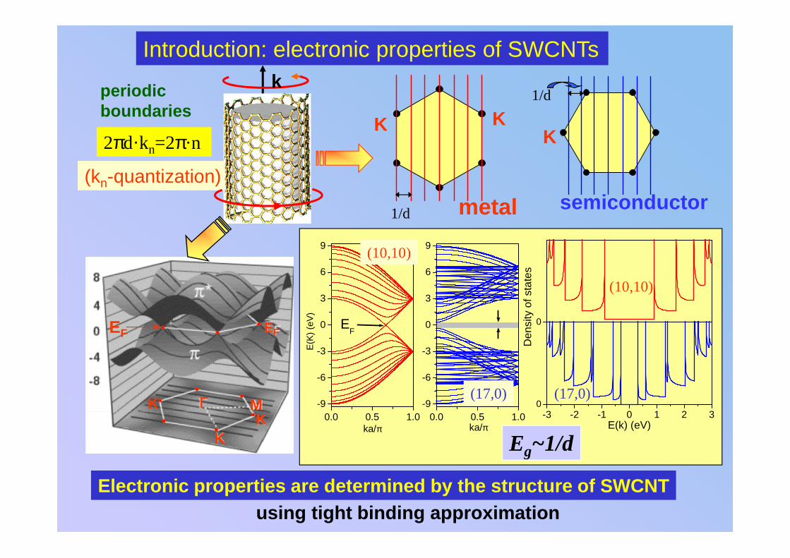
SWCNTs Hamada vector
(n,n) armchair
(n,0) zigzag
(n,m) chiral
(n,0)
(n,n)
a2
Φ
Introduction: formation of single-wall carbon nanotubes
Φ=0Φ=0Φ=0Φ=0
Φ=30Φ=30Φ=30Φ=30°°°°
0<Φ<300<Φ<300<Φ<300<Φ<30°°°°dn,m=|C|/ππππ=a(n2+m2+mn)1/2/ππππThe diameter of SWCNT (n,m) :
a=|a1|=|a2|=2.49 Å
graphene sheet
e.g. (10,10) d=1.37nm
o
A
O(A)
����
),(21 mnamanC =+= rrr
����C
����C
����a1
(n,m)
d
0.0 0.5 1.0-9
-6
-3
0
3
6
9
0.0 0.5 1.0-9
-6
-3
0
3
6
9
EF
E(K
) (e
V)
ka/π ka/π
0
-3 -2 -1 0 1 2 30
D
ensi
ty o
f sta
tes
E(k) (eV)
Introduction: electronic properties of SWCNTs
semiconductor
2πd·kn=2π·n
1/d
1/d
Eg~1/d
(10,10)
(17,0)
K KK
(kn-quantization)
Electronic properties are determined by the structu re of SWCNT
periodic boundaries
k
metal
(10,10)
(17,0)
EF
KM
K
K ΓΓΓΓ
EF
using tight binding approximation

Synthesis and purification of SWCNT and DWCNT.high vacuum CVD!
Electronic/optical properties: EELS, XAS,ARPES,Raman, PL,OAS!What happens upon functionalization?
Charge transfer vs. hybridisation: bonding environment, doping level, Fermi level shift and changes in the DOS.
Nature of the metallic ground state:
Normal Fermi liquid or a Tomonaga-Luttinger liquid?Transition 1D – 3D metal?
Electronic structure of functionalized SW(DW)CNT from high energy and optical spectroscopy
What are we doing on nanotubes ….. ?

SWCNT from laser ablation/ arc discharge
SWCNT yield and diameter distribution vs. T, p, laser pulse, gas, catalyst, …
Optimised: 70 wt% SWCNT, d=1.2-1.4 nm
Purification andopening:HNO3, H2O2,Heat treatment
semiconductingmetallic
SWCNT with no catalyst and “carbon impurities”, d=1.4 +/- 0.12 nm

Optical response of type separated bulk SWCNT
Y. Miyata et al., J. Phys. Chem. C 2008, 112, 3591 (2008)

-2 -1 0 1 2
S3,4
S*
2
S*
1
M*1
M1
S1
S2
Energy (eV)
DO
S
SemiconductingMetal
S3,4
M2,3
M*2,3
*
diameter
1.37 ± 0.08nm
Miyata et al. J Phys. Chem.C 112, 13187 (2008).
Samples

Gain from High Energy Spectroscopy
Photoemission Spectroscopy X-ray absorption and EELS
Occupied Density of States Unoccupied Density of States
Matrix element weighted DOSValence Band Conduction Band
(site selective)(site selective for RESPES)
Core Hole Effects!!!
Bonding environment
Charge Transfer
Basic Correlation Effects
Bonding environment
Charge Transfer
Basic Correlation Effects

Core Level High resolution XPS
-Doniac-Sunjic lineshape M
-Voigtian (symetric) SC
285.2 284.8 284.4 284.0 N
orm
aliz
ed In
tens
ity Binding Energy (eV)
METALLICITY MIXED SWCNT
Kramberger et al. PRB 75 (2007) 235437
0,4eV

High resolution XPS of metallicity sorted SWCNT
P.Ayala et. al. PRB 80 (2009) 205427
Core hole screening not visibly affected in metallic samples
Work functions : different in bulk metallic SWCNTs sample
Graphite
0,32 eVDoniach Sunjic
Voigtian

π*
σπ
C1s
σ*
π
π*
C 1s
EF
0 D2 D
kWhat is the electronic behavior of the 1 D system??

k
0 D
1 D
2 D
10 8 6 4 2 0
σσσσC60
SWCNTs
N
orm
aliz
ed In
tens
ity
Energy (eV)
ππππ
Graphite
High Energy Spectroscopy studies on sp2 –hybridized C structures
Site selective weighted projected DOS of the conduction band
285 290 295
σσσσ∗∗∗∗ππππ∗∗∗∗
Nor
mal
ized
Inte
nsity
Energy (eV)
VB-PES Conduction Band-XAS
Matrix element weighted DOS of the valence band
283 284 285 286 287 288
Mea
sure
d+
reso
l. br
oad.
Cal
c. D
OS
Energy (eV)C1s
π*
σ*
π
σ
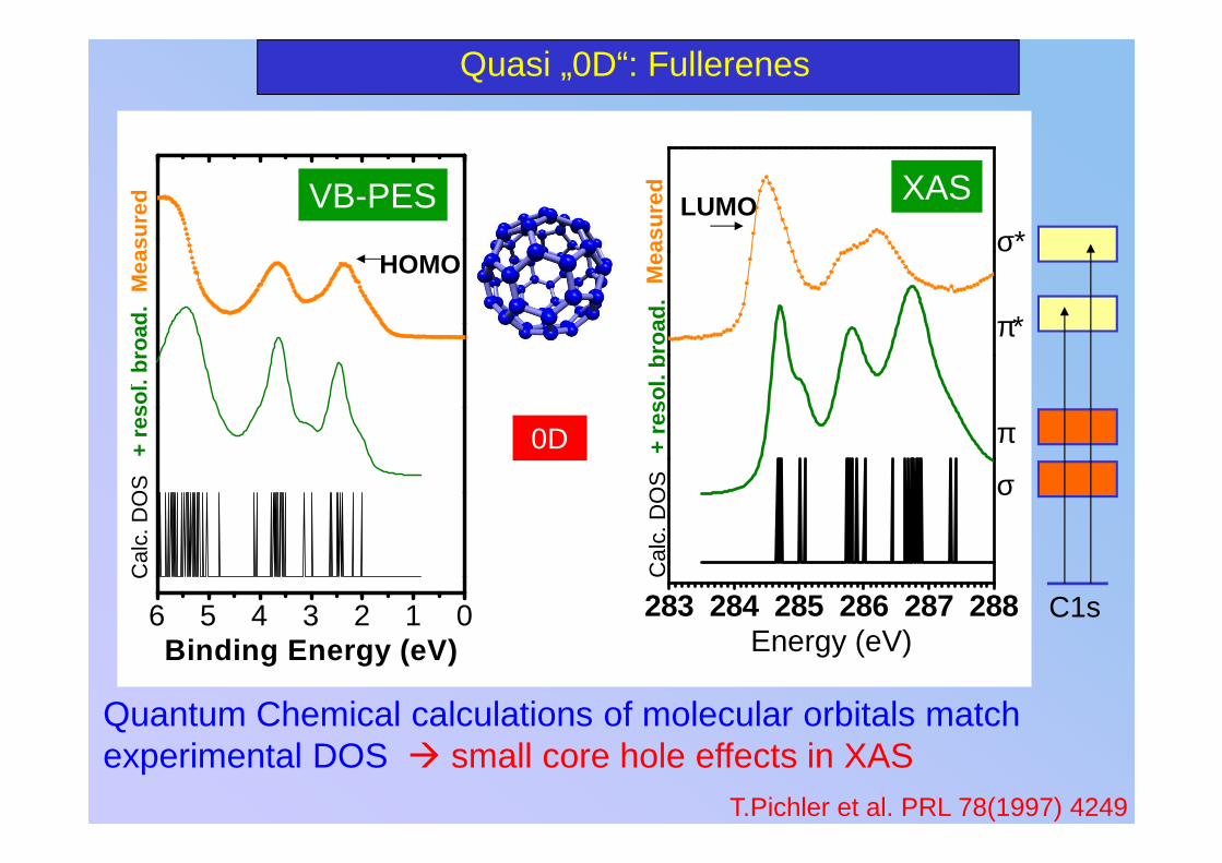
Quasi „0D“: Fullerenes
Quantum Chemical calculations of molecular orbitals match experimental DOS � small core hole effects in XAS
0D
6 5 4 3 2 1 0
+ re
sol.
broa
d.M
easu
red
Cal
c. D
OS
Binding Energy (eV)
VB-PES XAS
HOMO
LUMO
T.Pichler et al. PRL 78(1997) 4249

2D: Graphite-Graphene
π
π*
C 1s
EF
2D
But: strong core hole effects in XAS of the conduction band
ππππ
TB-DOS of the valence band matches experimental DOS
VB-PES XAS
Bruhwiler et al.PRL 76
(1996)1761
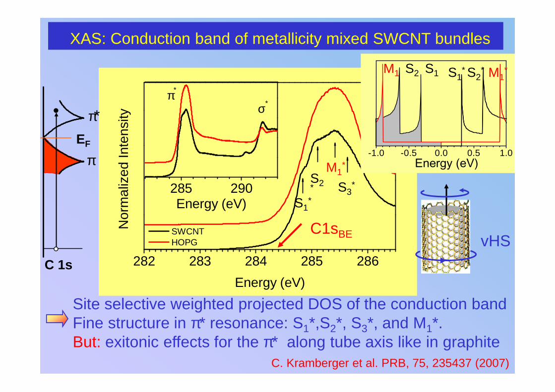
XAS: Conduction band of metallicity mixed SWCNT bundles
Site selective weighted projected DOS of the conduction band Fine structure in π* resonance: S1*,S2*, S3*, and M1*. But: exitonic effects for the π* along tube axis like in graphite
282 283 284 285 286
285 290
SWCNT HOPG
Nor
mal
ized
Inte
nsity
Energy (eV)
π∗
Energy (eV)
σ∗
S1*
S2*
M1*
C1sBE
S3*
-1.0 -0.5 0.0 0.5 1.0
S2M1
Energy (eV)
M1*S1
* S2*S1
C. Kramberger et al. PRB, 75, 235437 (2007)
π
π*
C 1s
EF
vHS

vHS in DOS of conduction band: XAS fine structure
Strong excitonic effect on π* resonance (parallell), vHS only weakly affected
284 285 286 287 284 285 286 287
0 1 2 3 0 1 2 3
M*
4M*
2,3M*
1
b)
S*
2S*
3
Nor
mal
ized
Inte
nsity
Energy (eV)
ππππ∗∗∗∗
a)
S*
5
Nor
mal
ized
Inte
nsity
Energy (eV)
S*
1
ππππ∗∗∗∗
DO
S
Energy (eV)
S*
4DO
S
Energy (eV)
P. Ayala et al. PRB80, 205427 (2009)
π
π*
C 1s
EF

Valence band of a metallicity mixed SWCNT bucky paper
π
σ
High resolution angle integrated photoemission at T=35 K:
10 8 6 4 2 0
Inte
nsity
(ar
b. u
nits
)
Binding energy (eV)vHS of tubes: S1, S2, M1good agreement with TB calculations e.g. H. Ishii et al, Nature, 426, 540 (2003), H. Rauf et al.
1.5 1.0 0.5 0.0
Binding energy (eV)
M1S2
S1
-1.0 -0.5 0.0 0.5 1.0
S2 S1M1
Energy (eV)
M1*S1
* S2*

Diameter cumulative DOS in VB photoemission response
Very good agreement between PES peaks and diameter cumulative DOS!Additional life time broadening in experiment!Chemical potential for semiconducting tubes shifted by 0.1 eV!No Fermi edge in metallic SWCNT
4 3 2 1 0 4 3 2 1 0
4 2 0 -2 -4 4 2 0 -2 -4
0.5 0.0
b)
M2,3
Inte
nsity
(cp
s)
Binding energy (eV)
EF
π
M1
a)
S3,4,5
S2
Inte
nsity
(cp
s)Binding energy (eV)
EF
π
S1
DO
S
Energy (eV)
DO
S
Energy (eV)
Energy (eV)
P. Ayala et al. PRB80, 205427 (2009)
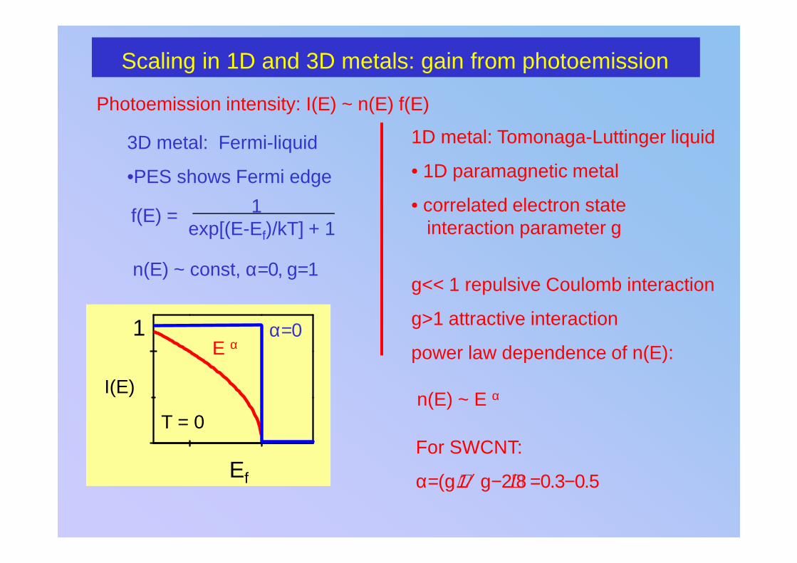
Scaling in 1D and 3D metals: gain from photoemission
Ef
1exp[(E-Ef)/kT] + 1
f(E) =
n(E) ~ E α
I(E)
1
T = 0
3D metal: Fermi-liquid
•PES shows Fermi edge
1D metal: Tomonaga-Luttinger liquid
• 1D paramagnetic metal
• correlated electron state interaction parameter g
g<< 1 repulsive Coulomb interaction
g>1 attractive interaction
power law dependence of n(E):
Photoemission intensity: I(E) ~ n(E) f(E)
n(E) ~ const, α=0, g=1
For SWCNT:
α=(g+1/g−2)/8 =0.3−0.5
α=0E α

Metallic tubes in metallicity mixed samples
T = 35K
α = 0.43, g=0.18
good agreement with theoretical predictions and results from transport measurements
1.5 1.0 0.5 0.0
0.2 0.02
log
Inte
nsity
(ar
b. u
nits
)
In
tens
ity (
arb.
uni
ts)
Binding energy (eV)
log Binding energy (eV)
α = 0.43
S1
S2
M1
Metallic SWCNT in a bundle of SWCNThave the renormalization of a Tomonaga-Luttinger liquid
semiconductingmetallic
H. Ishii et al, Nature, 426, 540 (2003); H. Rauf et al, PRL 93, 096805 (2004)

A bundle of undoped metallic SWCNT
� Undoped purely metallic SWCNT bundles are still 1D metals
No Fermi liquid!No Fermi edge for metallic SWCNT!
�Still van der Waals interaction of the tubes in a bundle!
� Implications on maximum conductivity in e.g. transparent electrodes
P. Ayala et al. PRB80, 205427 (2009)
1.5 1.0 0.5 0.0
1 0.1 0.01
log
Inte
nsity
(ar
b. u
nits
)
In
tens
ity (
arb.
uni
ts)
Binding energy (eV)
M1
log BE (eV)
αααα = 0.37

Intercalation
in-situ doping: UHV evaporation(5x10⁻¹⁰ mbar)Na, K, Rb, Cs and Ba SAES getters
getter
vapor
Sapphirefilm
Alkali-metal intercalation
UHVdoping
e-
e--2 -1 0 1 2
0.0
0.1
(10,10)D
OS
(eV
-1C
-1)
Energy (eV)

INTERCALATION:
doping
SCM
What happens with doping?

INTERCALATION:
doping
SCM
Is a bundle of doped metallic tubes a normal Fermi liquid or a Luttinger liquid?
What happens with doping?

Transition from a TLL to a FL
0,10 0,05 0,00 -0,05
1:20
pristine
Inte
nsity
(ar
b. u
nits
)
Binding energy (eV)
metal T=35K
Crossover to a Fermi liquid
α = 0.43
α = 0
H. Rauf et al, PRL 93, 096805 (2004)
Dependence of the power law scaling factor alpha from the degree of doping.

Where is the transition from a TLL to a FL?
0,10 0,05 0,00 -0,05
1:20
pristine
Inte
nsity
(ar
b. u
nits
)
Binding energy (eV)
metalT=35K
α = 0.43
α = 0
1,5 1,0 0,5 0,0
1 0,1 0,01
log
Inte
nsity
(ar
b. u
nits
)
Inte
nsity
(ar
b. u
nits
)
Binding energy (eV)
M1
log BE (eV)
αααα = 0.37
TLL
FL
?

Rigid band shift in metallicity mixed samples
• S1, S2 and M1 shift to higher binding energies
• power law behavior at first stable
• abrupt change at K:C = 1:125, ∆E(S1) = 0.37eV
T=35K
1.5 1.0 0.5 0.0
Inte
nsity
(ar
b. u
nits
)
Binding energy (eV)
S 2S1
M1
-1.0 -0.5 0.0 0.5 1.0
S2 S1M1 M1*S1
* S2*
1 0.1
Inte
nsity
(ar
b. u
nits
)
Binding energy (eV)
αααα = 0.43
αααα ~ 0T=35K

Doping dependence of the LL parameter α in mixed samples
0.000 0.005 0.0100.0
0.1
0.2
0.3
0.4
0.5
5
6
7
43
2o
1
∆Es1
=
0.37 eV
∆Es1
=0.3 eV
α
K / C
Power law scaling vs. intercalation:α= const. up to K/C=1/500, ∆ES1=0.25 eVα=0, g=1 above K/C=1/150, ∆ES1>0.35 eV
H. Rauf et al. PRL 93, 096805 (2004); C. Kramberger et al. PRB 79, 195442(2009)
-0.5
0.0
0.57
6 5432
1
Ene
rgy
(eV
)-1.0
-0.5
0.0
0.5
1.0
a bundle of only metallic tubes is a normal Fermi liquid!
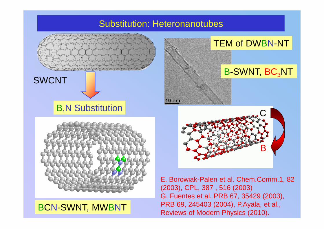
B,N Substitution
SWCNT
BCN-SWNT, MWBNT
Substitution: Heteronanotubes
TEM of DWBN-NT
E. Borowiak-Palen et al. Chem.Comm.1, 82 (2003), CPL, 387 , 516 (2003)G. Fuentes et al. PRB 67, 35429 (2003), PRB 69, 245403 (2004), P.Ayala, et al., Reviews of Modern Physics (2010).
B-SWNT, BC3NT
C
B

Filling@SWCNTso-called “peapod”
Filling of the inner space of SWCNTs with molecules
Filling
Modified electronic properties?
What happens upon the formation of the peapods?
Charge transfer, chemical bonding
or orbital hybridisation?
Conversion to double-wall carbon nanotubes (DWCNT)?
Potential applications
Carrier tuning of SWCNT, protection for molecules and even drugs, stabilizing reactive compounds and nanocrystals, chemical reaction inside a 1D confined nano reaction tube, 1D spinchain for spin electronics, …
?
?

Examples
Fullerenes@SWCNT
C60@SWCNT :
1D C60 chain inside SWCNT (TEM,Raman)
Gd@C82@SWCNT :
Band gap modulation (STM,STS)
Dy3N@C80@SWCNT :
Charge transfer (PES)
Conversion to DWCNT(TEM, Raman)!
Organic molecules @SWCNT
TCNQ, TDAE, Anthracene@SWCNT, Metallocenes p- and n- type doping
C60@SWCNT

Estimation of the local filling ratio by TEM
Peapods: e.g. C60 filled SWCNT
>90 % filling

C60 - C60 distance 9.7 Å no C60 polymer in SWCNT
X. Liu et al., Phys. Rev. B 65, 45419 (2002), Synth. Met. 135-136, 715 (2003)
Bulk filling ratio, structure in peapods
C60
Maximum filling ratio with C60: 100% no charge transfer to C60
C1s
π*
t1g
t1u

Ferrocene filling of SWCNT and transformation to DWCNT
High filling factor after long time annealing in at 150 C

Metallocene filling and chemistry inside SWCNT
Metallocenes : TM(C5H5)2, RE(C5H5)3
CH M
Metallocene consists of
TM: Transition metal atoms
RE: Rare-earth metal atoms
Planar aromatic ligand: C5H5
Electronic & magnetic & chemical properties varying with metal atoms.
0.6 nm
0.4 nm
M = Fe : Ferrocene
Most stable metallocene~ 1.4 nm
Suitable size to be filled inside SWCNT !!!

Metallocene filling: Filling factor
Assuming a 1D ferrocene chain inside SWCNT (d =1.4 nm) with adjacent ferrocene distance ~ 0.755 nm
Fe/C ratio ~ 0.003
Filling factor ~ 35 %
0.755 nm
d = 1.4 nm
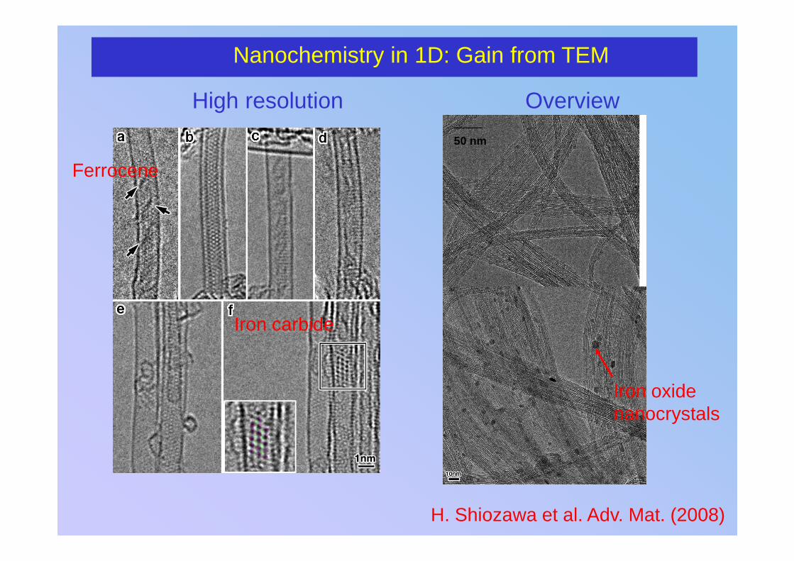
Nanochemistry in 1D: Gain from TEM
H. Shiozawa et al. Adv. Mat. (2008)
Ferrocene
Iron carbide
High resolution Overview
Iron oxide nanocrystals
50 nm

Ferrocene filled SWCNT and growth of DWCNT
• Charge transfer ∆EF=0.1 eV, ~0.2 e- per ferrocene• Power law behavior α =0.55• growth of inner tubes at ~ 600 °C
H. Shiozawa et al. Adv. Mat. (2008);PRB (2008)
2.0 1.5 1.0 0.5 0.0
720 710 300 290
x1
Fe2p
1/2
Norm
alize
d int
ensit
y
Binding energy (eV)
x20Fe
2p3/
2 C1s
Ferrocene
M1
S2
S1
B
A
Binding energy (eV)
Inte
nsity
(ar
b. u
nits
)
725 720 715 710 705
1150°C, 1h.
600°C, 2h.
FeCp2@NT
Nor
mal
ized
inte
nsity
Binding energy (eV)150 200 250 300 350
FeCp2@NT
1150°C, 1h.
Nor
mal
ized
inte
nsity
Raman shift (cm-1)
600°C, 2h.
SWCNT

290 300 310 320 330 340 350 360
(6,4)
(17,
3),(
15.6
)
(16,
2), (
14,5
), (
17,0
)
(14,
7),(
18,1
)
(13,
8),(
16,4
)
(12,
9),(
11,1
0)(1
7,2)
,(15
,5),
(18,
0)
(14,
6),(
16,3
),(1
3,7)
(17,
1),(
12,8
)
(14,
6) (11,
9),(
15,4
),(1
0,10
)
Nor
mal
ized
inte
nsity
Raman shift (cm -1)
(13,
6)
S
(16,
3)
(6,5)
0.60 0.65 0.70 0.75
Diameter difference (nm)N
orm
aliz
ed in
tens
ity
FeCp2@NT, 1150°C, 1h.
b C60
@NT, 1150°C, 15h.
(6,5)
(6,4)
DWCNT/Inner tubes: Gain from high resolution Raman
H. Shiozawa et al. Adv. Mat. (2008)Catalytic growth of inner DWCNT differs from non-catalytic!
Ferrocene
C60

Temperature induced chemical reaction in a SWCNT nanoreactor
H. Shiozawa et al. Adv. Mat. (2008); PRB (2008)
1. Ferrocene filling
MD simulation from S. Maruyama
2. Catalytic growth fromIron carbide particles
3. Iron release via defectsIron oxide nanocrystals
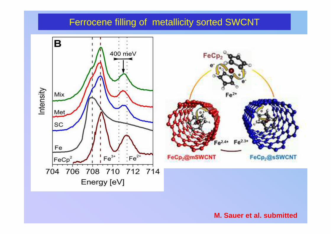
Ferrocene filling of metallicity sorted SWCNT
M. Sauer et al. submitted

PL of ferrocene filled Hipco SWCNT
Pristine Opened Filled
X. Liu et al. Advanced Functional Materials DOI: 10.1002/adfm.201200224 (2012)

PL of ferrocene filled Hipco SWCNT
X. Liu et al. Advanced Functional Materials DOI: 10.1002/adfm.201200224 (2012)

Summary for carbon nanostructures
Graphene and SWCNT are ideal 1D and 2D objects
Outstanding mechanical and electronic properties
Ideal systems to study basic correlation effectseven at room temperature!!!!!!
Tuneable electronic properties and interactions!!!
Interesting for both basic research and applications

….. and now finally to something completely different….
….. It´s …..

WANTED: PhD students, postdoc eager to unravel the equilibrium ground state dressed by correlations……!
The beauty of instabilities…!!!
My research groupin Vienna:
LOW DIMENSIONALQUANTUM SOLIDS

Gd@C82@SWCNTs undergo structural transformation upon heat treatment , yielding 1D Gd encapsulated nanowires.
82Gd@C82@SWCNTs→Gd@SWCNTs
P.Ayala et al., Materials Express 1,30 (2011).

• XAS response in the 3d levels of Gd and RESPES.• Stronger resonance for Gd nanowires � smaller hybridisation
82Gd@C82@SWCNTs→Gd@SWCNTs
P.Ayala et al., , Materials Express 1,30 (2011).
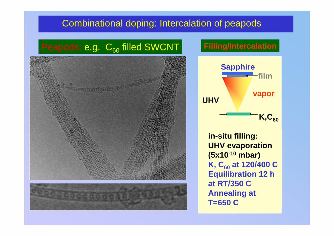
Combinational doping: Intercalation of peapods
Peapods: e.g. C60 filled SWCNT
in-situ filling: UHV evaporation(5x10⁻¹⁰ mbar)K, C60 at 120/400 CEquilibration 12 h at RT/350 CAnnealing at T=650 C
K,C60
vapor
Sapphirefilm
Filling/Intercalation
UHV
Okada et al. PRB 67, 205411;PRL 86, 3835
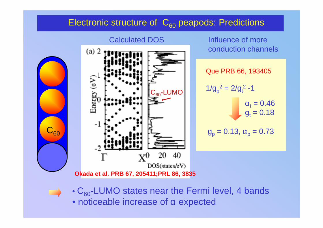
Electronic structure of C60 peapods: Predictions
Que PRB 66, 193405
1/gp2 = 2/gt
2 -1
αt = 0.46gt = 0.18
gp = 0.13, αp = 0.73
Calculated DOS Influence of more conduction channels
• C60-LUMO states near the Fermi level, 4 bands• noticeable increase of α expected
C60
C60-LUMO
9 8 7 6 5 4 3 2 1 0
In
tens
ity (
arb.
uni
ts)
Binding energy (eV)
pristine SWCNT pristine peapods
π
σ
hu=2.3 eV
HOMO-3,4 hg+gg=3.5 eV
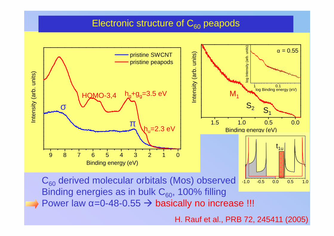
Electronic structure of C60 peapods
C60 derived molecular orbitals (Mos) observedBinding energies as in bulk C60, 100% fillingPower law α=0-48-0.55 � basically no increase !!!
1.5 1.0 0.5 0.0
1 0.1
log
Inte
nsity
(ar
b. u
nits
)
Inte
nsity
(ar
b. u
nits
)
Binding energy (eV)
log Binding energy (eV)
α = 0.55
M1
S2 S1
-1.0 -0.5 0.0 0.5 1.0
t1u
H. Rauf et al., PRB 72, 245411 (2005)
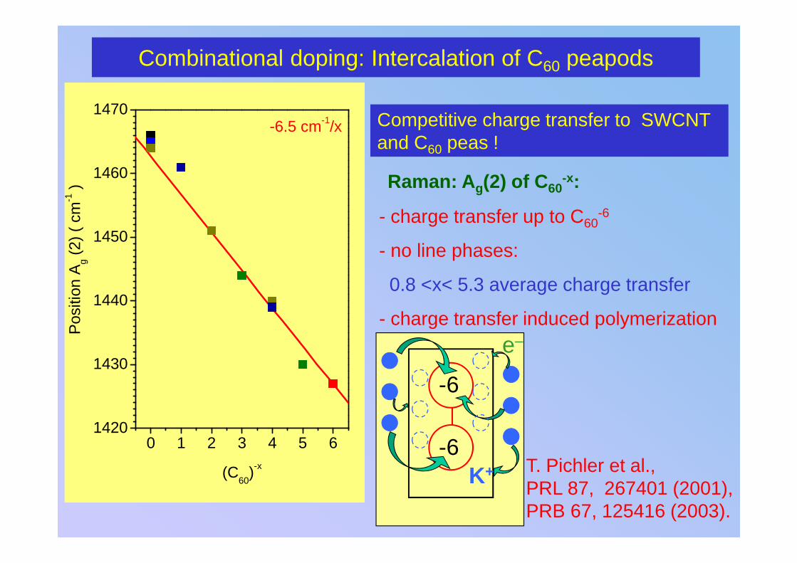
Combinational doping: Intercalation of C60 peapods
Competitive charge transfer to SWCNT and C60 peas !
Raman: A g(2) of C 60-x:
- charge transfer up to C60-6
- no line phases:
0.8 <x< 5.3 average charge transfer
- charge transfer induced polymerization
0 1 2 3 4 5 61420
1430
1440
1450
1460
1470-6.5 cm-1/x
Pos
ition
Ag
(2)
( cm
-1 )
(C60
)-x
-6
-6K+
e–
T. Pichler et al., PRL 87, 267401 (2001), PRB 67, 125416 (2003).

Why carbon nanotubes?
Archetypical 1D system:
New electronic, optical and structural properties:
- Ideal 1D quantumwires- Hard, ductile Nanowires- Molecular Magnets, Spintronics- Protection for reactiveelements and molecules
- Gas storage, gas sensing- FET, VIAS, optoelectronic- Sources for field emission- Organic superconductors- Li-Ion batteries- Sensors, actuators, NT-yarns, composits, drug delivery…..
Ideal tools for nanoelectronics/optics/mechanics/(bio)chemistry


