T800 Manual Rev 2 - RF Technology T800.pdfRF Technology T800 Page 5 1 OPERATING INSTRUCTIONS WARNING...
29
Eclipse Ser ies RF Technology [email protected] September 2003 Revision 2 T800 Transmitter Operation and Maintainance Manual This manual is produced by RF Technology Pty Ltd 10/8 Leighton Place, Hornsby NSW 2077 Australia Copyright © 1997, 1998, 2003 RF Technology
Transcript of T800 Manual Rev 2 - RF Technology T800.pdfRF Technology T800 Page 5 1 OPERATING INSTRUCTIONS WARNING...

Eclipse Ser ies
September 2003 Revision 2
T800 TransmitterOperation and Maintainance Manual
This manual is produced by RF Technology Pty Ltd10/8 Leighton Place, Hornsby NSW 2077 Australia
Copyright © 1997, 1998, 2003 RF Technology

___________________________________________________________________________RF Technology T800 Page 2
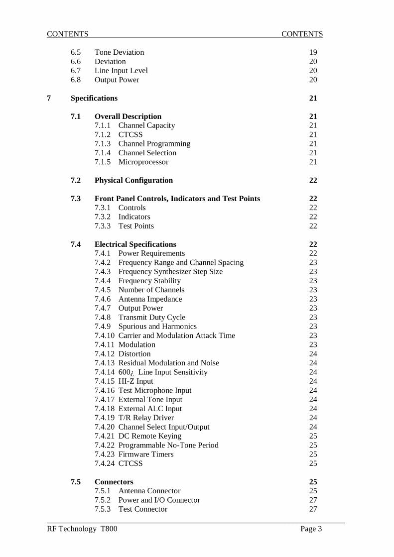
CONTENTS CONTENTS
1. Operating Instructions 51.1 Front Panel controls and Indicators 5
1.1.1 PTT 51.1.2 Line 51.1.3 PWR LED 51.1.4 TX LED 51.1.5 ALARM LED 61.1.6 ALC LED 61.1.7 REF LED 61.1.8 TEST MIC 6
2. Transmitter Internal Jumper Options 72.1 JP2: EPROM Type 72.2 JP3: Dc Loop PTT 72.3 JP4: Audio Input source 72.4 JP5: 600 ¿ Termination 72.5 JP6: Input Level Attenuation 82.6 JP7: Audio Frequency Response 82.7 JP8: Subaudible Tone Source 82.8 JP9, JP10, JP11 dc Loop PTT Input Configuration JP3 (1-2) 82.9 JP16: Direct Digital Input (Rev 4 or Higher) 82.10 JP17: Bypass Low Pass Filter (Rev 4 or Higher) 92.11 JP19: Alarm Output (Rev 4 or Higher) 92.12 JP22: Use Tone- as a Direct Digital Input (Rev 4 or Higher) 92.13 JP23: Connection of DMTX Board (Rev 4 or Higher) 9
3. Transmitter Internal Jumper Options3.1 25 Pin Connector 103.2 Rear Panel Connectors 11
4. Channel and Tone Frequency Programming 12
5. Circuit Description 135.1 VCO Section 135.2 PLL Section 135.3 Power Amplifier 145.4 Temperature Protection 145.5 600 ¿ Line Input 145.6 Direct coupled Audio Input 145.7 Local Microphone Input 155.8 CTCSS and Tone Filter 155.9 Audio Signal Processing 155.10 PTT and DC Remote Control 165.11 Microprocessor Controller 165.12 Voltage Regulator 17
6. Field Alignment Procedure 176.1 Standard Test Conditions 186.2 VCO Alignment 186.3 TCXO Calibration 186.4 Modulation Balance 19
___________________________________________________________________________RF Technology T800 Page 3
CONTENTS CONTENTS
6.5 Tone Deviation 196.6 Deviation 206.7 Line Input Level 206.8 Output Power 20
7 Specifications 21
7.1 Overall Descr iption 217.1.1 Channel Capacity 217.1.2 CTCSS 217.1.3 Channel Programming 217.1.4 Channel Selection 217.1.5 Microprocessor 21
7.2 Physical Configuration 22
7.3 Front Panel Controls, Indicators and Test Points 227.3.1 Controls 227.3.2 Indicators 227.3.3 Test Points 22
7.4 Electrical Specifications 227.4.1 Power Requirements 227.4.2 Frequency Range and Channel Spacing 237.4.3 Frequency Synthesizer Step Size 237.4.4 Frequency Stability 237.4.5 Number of Channels 237.4.6 Antenna Impedance 237.4.7 Output Power 237.4.8 Transmit Duty Cycle 237.4.9 Spurious and Harmonics 237.4.10 Carrier and Modulation Attack Time 237.4.11 Modulation 237.4.12 Distortion 247.4.13 Residual Modulation and Noise 247.4.14 600¿ Line Input Sensitivity 247.4.15 HI-Z Input 247.4.16 Test Microphone Input 247.4.17 External Tone Input 247.4.18 External ALC Input 247.4.19 T/R Relay Driver 247.4.20 Channel Select Input/Output 247.4.21 DC Remote Keying 257.4.22 Programmable No-Tone Period 257.4.23 Firmware Timers 257.4.24 CTCSS 25
7.5 Connectors 257.5.1 Antenna Connector 257.5.2 Power and I/O Connector 277.5.3 Test Connector 27

___________________________________________________________________________RF Technology T800 Page 4
CONTENTS CONTENTS
A Engineering DiagramsA1 Block DiagramA2 Circuit DiagramA3 Component Overlay Diagram
B Parts List

___________________________________________________________________________RF Technology T800 Page 5
1 OPERATING INSTRUCTIONS
WARNING
Changes or modifications not expressly approved byRF Technology could void your authority to operate thisequipment. Specifications may vary from those given inthis document in accordance with requirements of local
authorities. RF Technology equipment is subject tocontinual improvement and RF Technology reserves theright to change performance and specification without
further notice.
1 Operating Instructions
1.1 Front Panel Controls and Indicator s
1.1.1 PTT
A front-panel push-to-talk (PTT) button is provided to facilitate bench and field tests andadjustments. The button is a momentary action type. When keyed, audio from the line inputis disabled so that a carrier with sub-tone is transmitted. The front-panel microphone input isnot enabled in this mode, but it is enabled when the PTT line on that socket is pulled toground.
1.1.2 Line
The LINE trimpot is accessible by means of a small screwdriver from the front panel of themodule. It is used to set the correct sensitivity of the line and direct audio inputs. It isfactory preset to give 60% of rated deviation with an input of 0dBm (1mW on 600Ωequivalent to 775mV RMS or about 2.2V peak-to-peak) at 1kHz. The nominal 60% deviationlevel may be adjusted by measuring between pins 6 and 1 on the test socket, and adjusting thepot. By this means an input sensitivity from approximately -30dBm to +10dBm may beestablished.
An internal jumper provides a coarse adjustment step of 20dB. Between the jumper and thetrimpot, a wide range of input levels may be accommodated.
1.1.3 POWER LED
The PWR LED shows that the dc supply is connected to the receiver.
1.1.4 TX LED
The TX LED illuminates when the transmitter is keyed. It will not illuminate (and an Alarmcadence will be shown) if the synthesizer becomes unlocked, or the output amplifier supply isinterrupted by the microprocessor.
___________________________________________________________________________RF Technology T800 Page 6
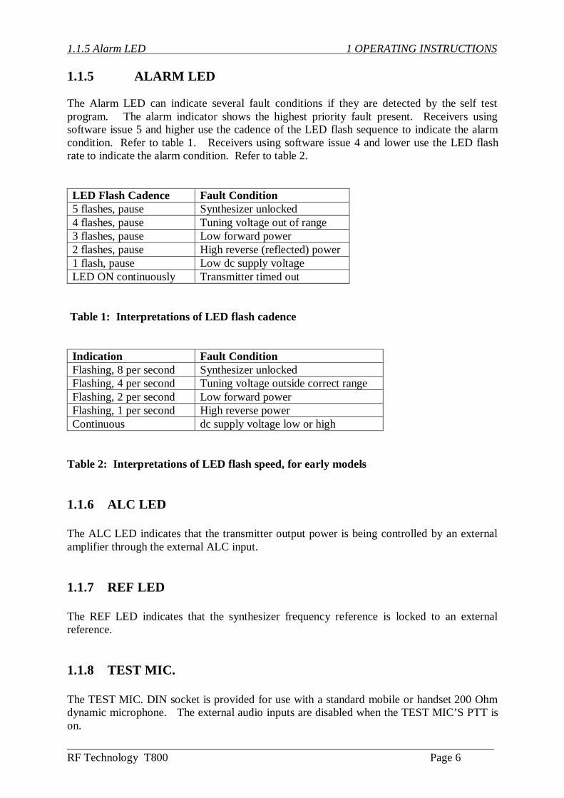
1.1.5 Alarm LED 1 OPERATING INSTRUCTIONS
1.1.5 ALARM LED
The Alarm LED can indicate several fault conditions if they are detected by the self testprogram. The alarm indicator shows the highest priority fault present. Receivers usingsoftware issue 5 and higher use the cadence of the LED flash sequence to indicate the alarmcondition. Refer to table 1. Receivers using software issue 4 and lower use the LED flashrate to indicate the alarm condition. Refer to table 2.
LED Flash Cadence Fault Condition5 flashes, pause Synthesizer unlocked4 flashes, pause Tuning voltage out of range3 flashes, pause Low forward power2 flashes, pause High reverse (reflected) power1 flash, pause Low dc supply voltageLED ON continuously Transmitter timed out
Table 1: Interpretations of LED flash cadence
Indication Fault ConditionFlashing, 8 per second Synthesizer unlockedFlashing, 4 per second Tuning voltage outside correct rangeFlashing, 2 per second Low forward powerFlashing, 1 per second High reverse powerContinuous dc supply voltage low or high
Table 2: Interpretations of LED flash speed, for ear ly models
1.1.6 ALC LED
The ALC LED indicates that the transmitter output power is being controlled by an externalamplifier through the external ALC input.
1.1.7 REF LED
The REF LED indicates that the synthesizer frequency reference is locked to an externalreference.
1.1.8 TEST MIC.
The TEST MIC. DIN socket is provided for use with a standard mobile or handset 200 Ohmdynamic microphone. The external audio inputs are disabled when the TEST MIC’S PTT ison.

___________________________________________________________________________RF Technology T800 Page 7
2 TRANSMITTER INTERNAL JUMPER OPTIONS
2 Transmitter Internal Jumper Options
In the following subsections an asterisk (*) signifies the standard (Ex-Factory) configurationof a jumper.
2.1 JP2: EPROM Type
Condition Position27C256 2-3 *27C64 1-2
2.2 JP3: 600 Ohm Line Dc Loop PTT Input
By default, Eclipse exciters can be keyed up by pulling the PTT signal low, or by dc loopsignalling on the audio pair.
This jumper enables or disables this second method.
Condition Positiondc loop connected (enabled) 1-2 *dc loop not connected (bypassed) 2-3
2.3 JP4: Audio Input Source Selection
Either the 600Ω or the high-Z balanced inputs may be selected.
Condition Position600Ω Input 2-3 *High-impedance Input 1-2
2.4 JP5: 600 ¿ Termination
Normally the Line Input is terminated in 600 ¿ . The 600 ohm termination can be removedby choosing the alternate position.
Condition Position600¿ Termination 1-2*No Termination 2-3
___________________________________________________________________________RF Technology T800 Page 8
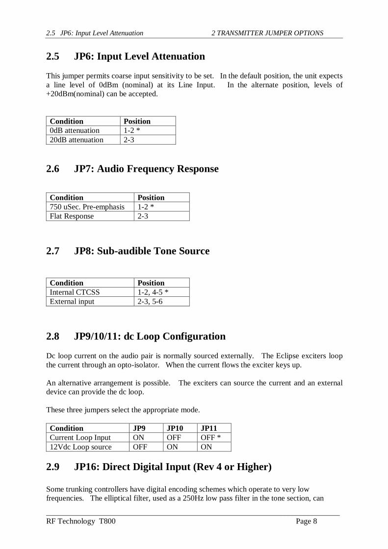
2.5 JP6: Input Level Attenuation 2 TRANSMITTER JUMPER OPTIONS
2.5 JP6: Input Level Attenuation
This jumper permits coarse input sensitivity to be set. In the default position, the unit expectsa line level of 0dBm (nominal) at its Line Input. In the alternate position, levels of+20dBm(nominal) can be accepted.
Condition Position0dB attenuation 1-2 *20dB attenuation 2-3
2.6 JP7: Audio Frequency Response
Condition Position750 uSec. Pre-emphasis 1-2 *Flat Response 2-3
2.7 JP8: Sub-audible Tone Source
Condition PositionInternal CTCSS 1-2, 4-5 *External input 2-3, 5-6
2.8 JP9/10/11: dc Loop Configuration
Dc loop current on the audio pair is normally sourced externally. The Eclipse exciters loopthe current through an opto-isolator. When the current flows the exciter keys up.
An alternative arrangement is possible. The exciters can source the current and an externaldevice can provide the dc loop.
These three jumpers select the appropriate mode.
Condition JP9 JP10 JP11Current Loop Input ON OFF OFF *12Vdc Loop source OFF ON ON
2.9 JP16: Direct Digital Input (Rev 4 or Higher )
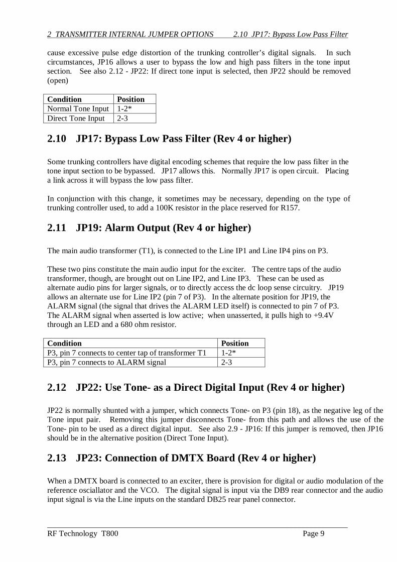
Some trunking controllers have digital encoding schemes which operate to very lowfrequencies. The elliptical filter, used as a 250Hz low pass filter in the tone section, can
___________________________________________________________________________RF Technology T800 Page 9
2 TRANSMITTER INTERNAL JUMPER OPTIONS 2.10 JP17: Bypass Low Pass Filter
cause excessive pulse edge distortion of the trunking controller’s digital signals. In suchcircumstances, JP16 allows a user to bypass the low and high pass filters in the tone inputsection. See also 2.12 - JP22: If direct tone input is selected, then JP22 should be removed(open)
Condition PositionNormal Tone Input 1-2*Direct Tone Input 2-3
2.10 JP17: Bypass Low Pass Filter (Rev 4 or higher )
Some trunking controllers have digital encoding schemes that require the low pass filter in thetone input section to be bypassed. JP17 allows this. Normally JP17 is open circuit. Placinga link across it will bypass the low pass filter.
In conjunction with this change, it sometimes may be necessary, depending on the type oftrunking controller used, to add a 100K resistor in the place reserved for R157.
2.11 JP19: Alarm Output (Rev 4 or higher )
The main audio transformer (T1), is connected to the Line IP1 and Line IP4 pins on P3.
These two pins constitute the main audio input for the exciter. The centre taps of the audiotransformer, though, are brought out on Line IP2, and Line IP3. These can be used asalternate audio pins for larger signals, or to directly access the dc loop sense circuitry. JP19allows an alternate use for Line IP2 (pin 7 of P3). In the alternate position for JP19, theALARM signal (the signal that drives the ALARM LED itself) is connected to pin 7 of P3.The ALARM signal when asserted is low active; when unasserted, it pulls high to +9.4Vthrough an LED and a 680 ohm resistor.
Condition PositionP3, pin 7 connects to center tap of transformer T1 1-2*P3, pin 7 connects to ALARM signal 2-3
2.12 JP22: Use Tone- as a Direct Digital Input (Rev 4 or higher )
JP22 is normally shunted with a jumper, which connects Tone- on P3 (pin 18), as the negative leg of theTone input pair. Removing this jumper disconnects Tone- from this path and allows the use of theTone- pin to be used as a direct digital input. See also 2.9 - JP16: If this jumper is removed, then JP16should be in the alternative position (Direct Tone Input).
2.13 JP23: Connection of DMTX Board (Rev 4 or higher )
When a DMTX board is connected to an exciter, there is provision for digital or audio modulation of thereference osciallator and the VCO. The digital signal is input via the DB9 rear connector and the audioinput signal is via the Line inputs on the standard DB25 rear panel connector.
___________________________________________________________________________RF Technology T800 Page 10
3.1 25 Pin Connector 3 TRANSMITTER I/O CONNECTIONS
Condition PositionNo DMTX board 1-2, 5-6*DMTX board connected 2-3, 4-5
In addition to the jumper changes, a wire link or zero ohm resistor must be connected in theplace marked for R159.
3 Transmitter I/O Connections
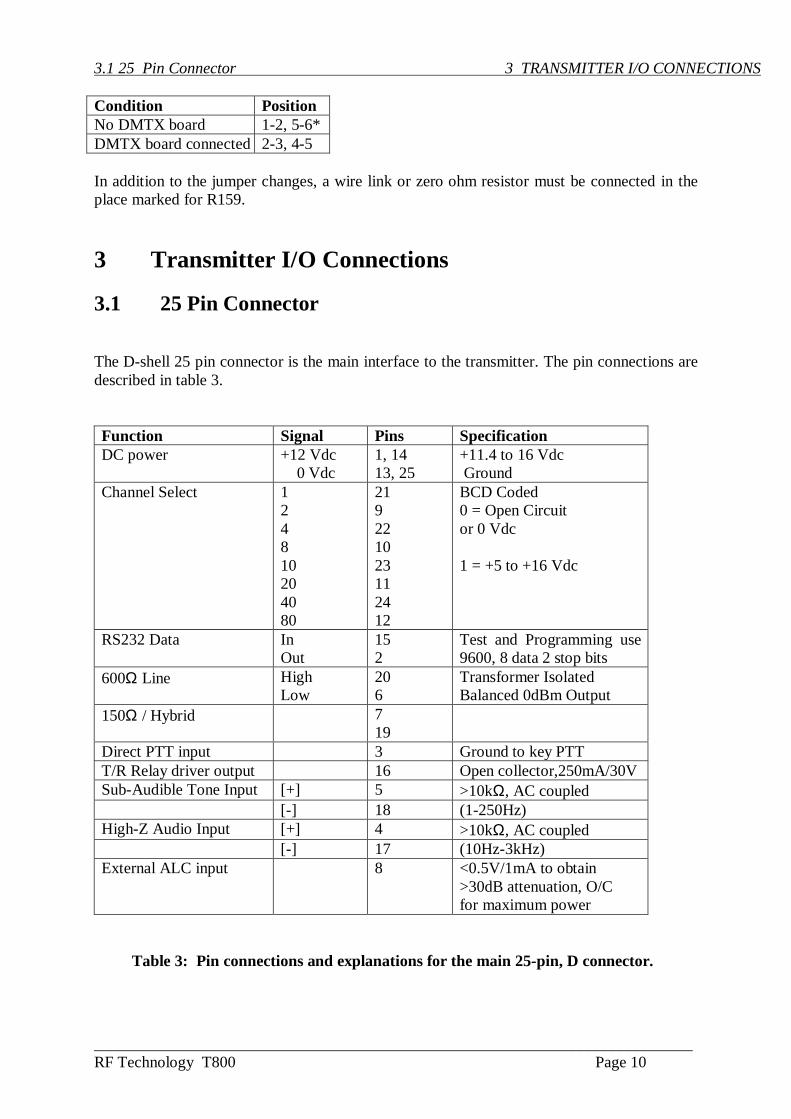
3.1 25 Pin Connector
The D-shell 25 pin connector is the main interface to the transmitter. The pin connections aredescribed in table 3.
Function Signal Pins SpecificationDC power +12 Vdc
0 Vdc1, 1413, 25
+11.4 to 16 Vdc Ground
Channel Select 124810204080
219221023112412
BCD Coded0 = Open Circuitor 0 Vdc
1 = +5 to +16 Vdc
RS232 Data InOut
152
Test and Programming use9600, 8 data 2 stop bits
600Ω Line HighLow
206
Transformer IsolatedBalanced 0dBm Output
150Ω / Hybrid 719
Direct PTT input 3 Ground to key PTTT/R Relay driver output 16 Open collector,250mA/30VSub-Audible Tone Input [+] 5 >10kΩ, AC coupled
[-] 18 (1-250Hz)High-Z Audio Input [+] 4 >10kΩ, AC coupled
[-] 17 (10Hz-3kHz)External ALC input 8 <0.5V/1mA to obtain
>30dB attenuation, O/Cfor maximum power
Table 3: Pin connections and explanations for the main 25-pin, D connector.

___________________________________________________________________________RF Technology T800 Page 11
3 TRANSMITTER I/O CONNECTIONS 3.2 Rear Panel Connectors
3.2 Rear Panel Connectors
The exciter and receiver can be supplied with optional rear panel connectors that bringout the more important signals available on P1, the rear panel DB25 connector.
Figures 1 and 2 show the rear panel connectors, and Table 4 shows the signals that are broughtout to the spade connectors. The spade connectors (2.1x0.6x7mm) are captive/solderedat the labelled points.
Fig 1 Fig 2 RX PCB TX PCB
The Receiver and Transmitter modules plug into the back plane DB25/F connectors
To configure: Solder wire connections between appropriate points.

___________________________________________________________________________RF Technology T800 Page 12
4 CHANNEL and TONE FREQUENCY PROGRAMMING
ReceiverDB25/F
RXPCB
DESCRIPTION TXPCB
TransmitterDB25/F
1, 14 +12V +12V DC SUPPLY +12V 1, 14
2 TXD TX Data TXD 2
15 RXD RX Data RXD 15
3 COR+ Carrier Operate Sw+ PressToTalk input PTT 3
16 COR- Carrier Operate Sw- Tx/Rx output T/R 16
4 TONE Subtone output Hi Z audio input+ AUD+ 4
17 AUDIO Audio output Hi Z audio input- AUD- 17
5 AGND Audio Ground Ext tone input+ TONE+ 5
18 DISC Discriminator output Ext tone input- TONE- 18
6 LINE+ Line output+ Line input+ LINE+ 6
20 LINE- Line output- Line input- LINE- 20
8 EXT SQ Ext Squelch input Auto Level Control ALC 8
13, 25 GND Ground, 0V GND 13, 25
21 BCD 1 Channel select 1’s digit BCD 1 21
9 BCD 2 Channel select 1’s digit BCD 2 9
22 BCD 4 Channel select 1’s digit BCD 4 22
10 BCD 8 Channel select 1’s digit BCD 8 10
23 BCD 10 Channel select 10’s digit BCD 10 23
11 BCD 20 Channel select 10’s digit BCD 20 11
24 BCD 40 Channel select 10’s digit BCD 40 24
12 BCD 80 Channel select 10’s digit BCD 80 12
4 Channel and Tone Frequency Programming
Channel and tone frequency programming is most easily accomplished with RF TechnologyTecHelp software or the Service Monitor 2000 software. This software can be run on an IBMcompatible PC and provides a number of additional useful facilities. DOS and 32-bit versionsare available.
TecHelp allows setting of the adaptive noise squelch threshold, provides a simple means ofcalibrating the forward and reverse power detectors, setting the power alarm preset levels, andenabling transmitter hang time and timeout time limits. TecHelp can be supplied by yourdealer, distributor or by contacting RF Technology directly.

___________________________________________________________________________RF Technology T800 Page 13
5 CIRCUIT DESCRIPTION 5.1 VCO Section
5 Circuit Descr iption
The following descriptions should be read as an aid to understanding the block and schematicdiagrams given in the appendix of this manual.
5.1 VCO Section
The Voltage Controlled Oscillator uses a bipolar junction FET Q19 which oscillates at therequired transmitter output frequency. Varactor diodes D25 and D26 are used by the PLLcircuit to keep the oscillator on the desired frequency. A second varactor diode D3 is used tofrequency modulate the VCO. Transistor Q20 is used as an active filter to reduce the noiseon the oscillator supply voltage.
The VCO is keyed ON by the microcontroller through Q10. It is keyed ON when any of thePTT inputs are active and OFF at all other times.
The VCO output is amplified and buffered by monolithic amplifiers MA2 and MA3 beforebeing fed to the PLL IC U6.
Amplifiers MA1, MA4 and MA5 increase the VCO output to approximately 10 mW to drivethe power amplifier. MA1 is not switched on until the PLL has locked and had time to settle.This prevents any momentary off channel transmission when the transmitter is keyed.
5.2 PLL Section
The frequency reference for the synthesiser is a crystal oscillator using transistors Q26 andQ27 and crystal Y3. The temperature stability is better than 5 ppm and it can be synchronisedto an external reference for improved stability. External reference option board 11/9119 isrequired when using an external reference.
A positive temperature coefficient thermistor, XH1, is used in versions intended for operationdown to -30 degrees Celsius. The thermistor heats the crystal's case to maintain itstemperature above -10 degrees thus extending the oscillator stability of 5 ppm down to -30degrees ambient.
Varactor diodes D27-30 are used to frequency modulate the oscillator. The processed transmitaudio signal from U7b varies the diodes bias voltage to modulate the reference frequency.This extends the modulation capability down to a few Hz for sub-audible tones and digitalsquelch codes. A two point modulation scheme is used with the audio also being fed to theVCO to modulate the higher audio frequencies.
The 12.8 MHz output of Q27 is amplified by Q28 and Q29 to drive the reference input of thePLL synthesiser IC U6. This IC is a single chip synthesiser which includes a 1.1 GHz pre-scaler, programmable divider, reference divider and phase/frequency detector. The frequencydata for U6 is supplied via a serial data link by the microcontroller.

___________________________________________________________________________RF Technology T800 Page 14
5.3 Power Amplifier 5 CIRCUIT DESCRIPTION
The phase detector output signals of U6 are used to control two switched current sources. Theoutput of the positive and negative sources Q3 and Q6, produce the tuning voltage which issmoothed by the loop filter components to bias the V.C.O. varactor diode D3.
5.3 Power Amplifier
The 10 mW output from the main board connects to the power amplifier board through a shortminiature 50Ω coaxial cable.
Q2 on the power amplifier board increases the signal to approximately200mW. The bias ofQ2 is controlled by Q1 and the power leveling circuitry to adjust the drive to the outputmodule U2.
U2 increases the power from the driver to 30 watts before it is fed to the directional coupler,low pass filter and output connector. The directional coupler detects the forward and reversepower components and provides proportional dc voltages which are amplified by U1a andU1b.
The forward power voltage from U1a and U1b are compared to the present DC referencevoltage from RV1. The difference is amplified by U1c, Q3 and Q4. The resulting controlvoltage supplies Q2 through R10, R12 and completes the power levelling control loop.
5.4 Temperature Pr otection
Thermistor RT1 on the power amplifier board is used to sense the case temperature of theoutput module U2. If the case temperature rises above 90 degrees C, the voltage across RT1will increase and transistor Q5 will be turned on. This reduces the dc reference voltage to thepower regulator which inturn reduces the outpower by 6-10dB.
5.5 600Ω Line Input
The 600Ω balanced line input connects to line isolation transformer T1. T1 has two 150Ωprimary windings which are normally connected in series for 600Ω lines. The dual primarywindings can be used to provide DC loop PTT signaling or a 2/4 wire hybrid connection. Allfour leads are available at the rear panel system connector.
The secondary of T1 can be terminated with an internal 600Ω load through JP5 or left un-terminated in high impedance applications.
5.6 Direct Coupled Audio Input
A high impedance (10kΩ) direct AC coupled input is available at the system connector. Thedirect coupled input connects to U9a which is configured as a unity gain bridge amplifier.
The bridge configuration allows audio signal inversion by interchanging the positive andnegative inputs and minimizes ground loop problems. Both inputs should be connected, withone lead going to the source output pin and the other connected to the source audio ground.

___________________________________________________________________________RF Technology T800 Page 15
5 CIRCUIT DESCRIPTION 5.7 Local Microphone Input
5.7 Local Microphone Input
The local microphone input is provided for use with a standard low impedance dynamicmicrophone. The microphone output is amplified by U9a before connecting to analogueswitch U10a. U10b inverts the local microphone PTT input to switch U10a ON when themicrophone PTT button is pressed. U10a is OFF at all other times.
The local microphone audio has priority over the other inputs. Activation of the localmicrophone PTT input switches OFF the audio from the line or direct inputs through D16 andU10c
5.8 CTCSS and Tone Filter
The CTCSS encoder module H1, under control of the main microprocessor U13, can encodeall 38 EIA tones and (on some models) additional commonly-used tones.
The tone output of H1 connects to jumper JP8 which is used to select either H1 or an externaltone source. The selected source is coupled to U9c which is a balanced input unity gainamplifier. The buffered tone from U9c is fed to 300 Hz low pass filter U7c.
On Rev 4 or later revisions, the low pass filter can be by passed by inserting a jumper ontoJP17.
RV3, the tone deviation trimmer, is used to adjust the level of the tone from U7c before it iscombined with the voice audio signal in the summing amplifier U7a.
Back to back diodes D4 and D5 limit the maximum tone signal amplitude to preventexcessive tone deviation when external tone sources are used.
The subtone amplifier, filter and limiter can be bypassed on Rev 4 or later exciters byremoving the link from JP22 and moving the link in JP16 to the alternate position.
5.9 Audio Signal Processing
Jumper JP4 selects either the line or direct input source. The selected source is thenconnected to JP6. JP6 can be removed to provide 20 dB attenuation when the input level isabove 10 dBm to expand the useful range of the line level trimmer RV4. The wiper of RV4 iscoupled to the input of the input amplifier U9d. U9d provides a voltage gain of ten beforeconnecting to the input of analogue switch U10c.
The outputs of U10a and U10c are connected to the frequency response shaping networksC52, R133 (for 750µs pre-emphasis) and C61, R55 (for flat response). JP7 selects the pre-emphasized or flat response.
The audio signal is further amplified 100 times by U7d. U7d also provides the symmetricalclipping required to limit the maximum deviation. The output level from U7d is adjusted byRV1, the deviation adjustment, before being combined with the tone audio signal in thesumming amplifier U7a.
___________________________________________________________________________RF Technology T800 Page 16
5.10 PTT and DC Remote Control 5 CIRCUIT DESCRIPTION
The composite audio from U7a is fed through the 3Khz low pass filter U7b. When the linkson JP23 are in their default state, the filtered audio is coupled to the TCXO voltage tuninginput and the modulation balance trimmer RV2. RV2, R99 and R98 attenuate the modulationsignal before applying it to the VCO via varactor D3.
When DMTX board option is required, Jumper JP23 allows the audio paths to be re-routed.The DMTX board provides for an external digital modulation input signal. When the twolinks on JP23 are positioned in the middle of the 6 pin header, the audio from the exciter ispassed to the DMTX board via pin 5 of JP15, where the signal is conditioned and thenreturned from the DMTX board via pin 2 of JP15, and passed to the two modulation points.
RV2 adjusts level of the audio used to modulate the VCO. This primarily effects the deviationof audio frequencies above 500 Hz. RV2 is used to balance the high and low frequencydeviation to obtain a flat frequency response relative to the desired characteristic.
5.10 PTT and DC Remote Control
Two main PTT inputs are provided. The first, a direct logic level input, is connected to pin 3of the system connector. The transmitter can be keyed by applying a logic low or ground onpin 3. Pin 3 connects to the PTT logic and microprocessor through D10.
DC current loop control can be used for remote PTT operation. The current loop can beconfigured by JP9, JP10 and JP11 for use with either a remote free switch or a remoteswitched source.
Opto-isolator ISO1 is used to isolate the loop current signal from the transmitter PTT logic.The loop current passes through the input of ISO1 and the output of ISO1 connects to the PTTlogic.
A bridge consisting of diodes D6, D8, D9 and D14 ensures correct operation regardless of thecurrent polarity. Q17 limits the current and D7 limits the voltage input of ISO1. Any lowvoltage current source capable of providing 2mA at 4V or switching circuit with less than4.8k¿ loop resistance can be used to switch the DC loop.
The test PTT button on the front panel and the local microphone PTT button will also key thetransmitter. Both of these also mute the line audio input. The microphone line also enablesthat audio input.
A DMTX board can also cause the exciter to key up. When TX (or TTL_TX) signal isreceived by the DMTX board, it pulls pin 6 of JP15 low, which in turn asserts thePTT_WIRE-OR signal, causing the microprocessor (U13) to key the exciter up.
5.11 Microprocessor Controller
The microprocessor controller circuit uses a single-chip eight bit processor and severalsupport chips. The processor U13 includes non-volatile EE memory for channel frequencies,tones, and other information. It also has an asynchronous serial port, a synchronous serialport and an eight bit analogue to digital converter.

___________________________________________________________________________RF Technology T800 Page 17
5 CIRCUIT DESCRIPTION 5.12 Voltage Regulator
The program is stored in U5, a CMOS EPROM. U4 is an address latch for the low orderaddress bits. U2 is used to read the channel select lines onto the data bus. U11 is an addressdecoder for U5 and U2. U3 is a supervisory chip which keeps the processor reset unless the+5 Volt supply is within operating limits. U1 translates the asynchronous serial port data tostandard RS232 levels.
The analogue to digital converter is used to measure the forward and reverse power, tuningvoltage and dc supply voltage.
If the processor detects that the PTT_WIRE_OR signal is asserted low, it will attempts to keythe exciter up. If will first attempt to key the VCO through Q10, and if the LD pin goes high,it will switch the 9.2 Volt transmit line through Q14 and Q16. asserting Q16 has the effect ofalso asserting the yellow Tx LED (D12) on the front panel, enabling the local 25W poweramplifier, and causing the T/R Relay output to be pulled low. D24 is 30 volt zener whichprotects Q25 from both excessive voltages or reverse voltages.
Should there be a problem with either the tuning volts, or the battery voltage, the VCOlocking, the forward power, or the reverse power, the microprocessor will assert the ALARMLED, through Q1. Depending on the setting of Jumper JP19, the ALARM signal can bebrought out on pin 7 of P3.
5.12 Voltage Regulator
The dc input voltage is regulated down to 9.4 Vdc by a discrete regulator circuit. The seriespass transistor Q23 is driven by error amplifiers Q8 and Q18. Q9 is used to start up theregulator and once the circuit turns on, it plays no further part in the operation.
The +5 Volt supply for the logic circuits is provided by an integrated circuit regulator U14which is run from the regulated 9.4 Volt supply.
Jumper JP18 is not normally fitted to the board, and is bridged with a 12mil track on thecomponent side of the board. It is provided so that the 9.4V load can be isolated from thesupply by the service department to aid in fault finding.
Jumpers JP20 and JP21 are also not normally fitted on the board, and are usually bridged witha 12mil track on the component side. They allow U14 to be isolated from its input, or itsoutput or both.
6 Field Alignment Procedure
The procedures given below may be used to align the transmitter in the field. Normally,alignment is only required when changing operating frequencies, or after componentreplacement.
The procedures below do not constitute an exhaustive test or a complete alignment of themodule, but if successfully carried out are adequate in most circumstances.

___________________________________________________________________________RF Technology T800 Page 18
6.1 Standard Test Condition 6 FIELD ALIGNMENT PROCEDURE
TCXO calibration may be periodically required owing to normal quartz crystal aging. A driftof 1ppm/year is to be expected.
Each alignment phase assumes that the preceding phase has been successfully carried out, orat least that the module is already in properly aligned state with respect to precedingconditions.
6.1 Standard Test Condition
The following equipment and conditions are assumed unless stated otherwise:
• AF signal generator with 600Ω impedance, 50-3000Hz frequency range, with level set to387mV RMS.
• Power supply set to 13.8Vdc, with a current capable of >5A.
• RF 50Ω load, 30W rated, return loss <-20dB.
• Jumpers set to factory default positions.
Alignment FrequencyModel Range Align FT800A 806-830 818MHzT800B 850-870 860MHzT800C 928-942 935MHz
6.2 VCO Alignment
1. Select a channel at the center frequency (half way between the highest and lowestfrequencies for the model in question).
2. Disconnect the Audio input (no signal input).
3. Key the PTT line.
4. Measure the voltage between pins 9 and 1 of the test socket (TUNE V), and adjust C99 to obtain 4.5±0.25V, while the TX LED is ON and the ALARM LED is OFF.
6.3 TCXO Calibration
1. Select a channel at the center frequency (half way between the highest and lowestfrequencies for the model in question).
2. Disconnect the Audio input (no signal input).

___________________________________________________________________________RF Technology T800 Page 19
6 FIELD ALIGNMENT PROCEDURE 6.4 Modulation Balance
3. Key the PTT line.
4. Measure the carrier frequency at the output connector, and adjust XO1 until the correctcarrier frequency is measured, ±50Hz.
6.4 Modulation Balance
1. Set RV3 fully counter clockwise (CCW) (sub-tone off).
2. Set RV1 fully clockwise (CW) (maximum deviation)
3. Set RV2 mid-position
4. Set JP7 for flat response
5. Set JP4 for Hi-Z input
6. Key the transmitter on
7. Set the audio input to 150Hz, 0dBm.(387mV)
8. Measure deviation and adjust RV4 (line Level) for a deviation of 5kHz (2.5kHz fornarrow band transmitters).
9. Set the audio input to 1.5kHz, 0dBm.
10. Adjust RV2 (Mod. Bal.) for a deviation of 5kHz (2.5kHz for narrow band transmitters).
11. Repeat steps 6-9 until balance is achieved.
12. Key the transmitter off.
13. Return JP7 to its correct setting.
14. Carry out the Deviation (section 6.6) and Tone Deviation (section 6.5) alignmentprocedures.
6.5 Tone Deviation
1. Remove the audio input.
2. Key the transmitter on
3. Adjust RV3 for the desired deviation in the range 0-1kHz.1 If sub-tone(CTCSS) coding is not to be used, adjust RV3 fully CCW.
_________________________1 The factory default is 500Hz for wide band (5kHz maximum deviation) and 250Hz for narrow band channels.

___________________________________________________________________________RF Technology T800 Page 20
6.6 Deviation 6 FIELD ALIGNMENT PROCEDURE
6.6 Deviation
1. Set RV4 (Line Level) fully clockwise (CW).
2. Set the audio to 1kHz, 0dBm, on the line input.
3. Key the transmitter on.
4. Adjust RV1 (Set Max. Deviation) for a deviation of 5kHz (2.5kHz for narrow bandtransmitters).
5. Key the transmitter off.
6. Carry out the Line Input Level alignment procedure (section 6.7)
6.7 Line Input Level
1. Set the audio to 1kHz, 0dBm, on the line input, or use the actual signal to betransmitted.
2. Key the transmitter on.
3. Adjust RV4 (line level) for 60% of system deviation (3kHz or 1.5kHz for narrow bandsystems).
4. If the test signal is varying, RV4 may be adjusted to produce a level of 234mV RMS or660mVp-p at the audio voltage test connector pin 6 to pin 1.
5. Key the transmitter off.
6.8 Output Power
1. No audio input is required
2. Key the transmitter on.
3. Adjust RV1 on the power amplifier PCB for the desired power level at the outputconnector. 2
4. Key the transmitter off.____________________2 Be sure to set the power below the rated maximum for the model of transmitter. If in doubt, allow 1.5dBcable and connector losses, and assume that the maximum rated power is 15W. This means no more than 10Wat the end of a 1m length of test cable. This pessimistic procedure is safe on all models manufactured at the timeof writing.
___________________________________________________________________________RF Technology T800 Page 21
7 SPECIFICATIONS 7.1 Overall Description
7 SPECIFICATIONS
7.1 Overall Descr iption
The transmitter is a frequency synthesized, narrow band FM unit, normally used to drive a 50watt amplifier. It can also be used alone in lower power applications.Various models allow 2-25W of output power to be set across a number of UHF frequencybands. All necessary control and 600Ω line interface circuitry is included.
7.1.1 Channel Capacity
Although most applications are single channel, it can be programmed for up to 100 channels,numbered 0 - 99. This is to provide the capability of programming all channels into all of thetransmitters used at a given site. Where this facility is used in conjunction with channel-setting in the rack, exciter modules may be “hot-jockeyed” or used interchangeably. This canbe convenient in maintenance situations.
7.1.2 CTCSS
Full EIA sub-tone capability is built into the modules. The CTCSS tone can be programmedfor each channel. This means that each channel number can represent a unique RF and tonefrequency combination.
7.1.3 Channel Programming
The channel information is stored in non-volatile memory and can be programmed via thefront panel test connector using a PC and RF Technology software.
7.1.4 Channel Selection
Channel selection is by eight channel select lines. These are available through the rear panelconnector. Internal presetting is also possible. The default (open-circuit) state is to selectchannel 00.
A BCD active high code applied to the lines selects the required channel. This can besupplied by pre-wiring the rack connector so that each rack position is dedicated to a fixedchannel. Alternatively, thumb-wheel switch panels are available.
7.1.5. Micropr ocessor
A microprocessor is used to control the synthesizer, tone squelch, PTT function and facilitatechannel frequency programming. With the standard software, RF Technology modules alsoprovide fault monitoring and reporting.
___________________________________________________________________________RF Technology T800 Page 22
7.2 Physical Configuration 7 SPECIFICATIONS
7.2 Physical Configuration
The transmitter is designed to fit in a 19 inch rack mounted sub-frame. The installed height is4 RU (178 mm) and the depth is 350 mm. The transmitter is 63.5 mm or two Eclipse moduleswide.
7.3 Front Panel Controls, Indicators, and Test Points
7.3.1 Contr ols
Transmitter Key - Momentary Contact Push Button
Line Input Level - screwdriver adjust multi-turn pot
7.3.2 Indicator s
Power ON - Green LED
Tx Indicator - Yellow LED
Fault Indicator - Flashing Red LED
External ALC - Green LED
External Reference - Green LED
7.3.3 Test Points
Line Input – Pin 6 + Ground (pin 1)
Forward Power – Pin 8 + Ground (pin 1)
Reverse Power – Pin 4 + Ground (pin 1)
Tuning Voltage – Pin 9 + Ground (pin 1)
Serial Data (RS-232) – Pins 2 / 3 + Ground (pin 1)
7.4 Electr ical Specifications
7.4.1 Power Requirements
Operating Voltage - 10.5 to 16 Vdc with output power reduced below 12 Vdc
Current Drain - 5A Maximum, typically 0.25A Standby
Polarity - Negative Ground
___________________________________________________________________________RF Technology T800 Page 23
7 SPECIFICATIONS 7.4.2 Frequency Range and Channel Spacing
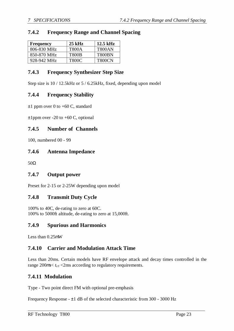
7.4.2 Frequency Range and Channel Spacing
Frequency 25 kHz 12.5 kHz806-830 MHz T800A T800AN850-870 MHz T800B T800BN928-942 MHz T800C T800CN
7.4.3 Frequency Synthesizer Step Size
Step size is 10 / 12.5kHz or 5 / 6.25kHz, fixed, depending upon model
7.4.4 Frequency Stability
±1 ppm over 0 to +60 C, standard
±1ppm over -20 to +60 C, optional
7.4.5 Number of Channels
100, numbered 00 - 99
7.4.6 Antenna Impedance
50Ω
7.4.7 Output power
Preset for 2-15 or 2-25W depending upon model
7.4.8 Transmit Duty Cycle
100% to 40C, de-rating to zero at 60C.100% to 5000ft altitude, de-rating to zero at 15,000ft.
7.4.9 Spur ious and Har monics
Less than 0.25µW
7.4.10 Car r ier and Modulation Attack Time
Less than 20ms. Certain models have RF envelope attack and decay times controlled in therange 200µs< tr/f <2ms according to regulatory requirements.
7.4.11 Modulation
Type - Two point direct FM with optional pre-emphasis
Frequency Response - ±1 dB of the selected characteristic from 300 - 3000 Hz
___________________________________________________________________________RF Technology T800 Page 24
7.4.12 Distortion 7 SPECIFICATIONS
Maximum Deviation - Maximum deviation preset to 2.5 or 5 kHz
7.4.12 Distor tion
Modulation distortion is less than 3% at 1 kHz and 60% of rated system deviation.
7.4.13 Residual Modulation and Noise
The residual modulation and noise in the range 300 - 3000 Hz is typically less than -50dBreferenced to rated system deviation.
7.4.14 600Ω Line Input Sensitivity
Adjustable from -30 to +10 dBm for rated deviation
7.4.15 HI-Z Input
Impedance - 10KΩ Nominal, balanced input
Input Level - 25mV to 1V RMS
7.4.16 Test Microphone Input
200Ω dynamic, with PTT
7.4.17 Exter nal Tone Input
Compatible with R500 tone output
7.4.18 Exter nal ALC Input
Output will be reduced 20dB by pulling the input down to below 1V. (Typically more than40dB attenuation is available.) The input impedance is ≅10kΩ, internally pulled up to rail.
The external ALC input can be connected to the power control circuit in Eclipse externalpower amplifiers.
7.4.19 T/R Relay Dr iver
An open collector transistor output is provided to operate an antenna change over relay orsolid state switch. The transistor can sink up to 250mA.
7.4.20 Channel Select Input / Output
Coding - 8 lines, BCD coded 00 - 99
Logic Input Levels - Low for <1.5V, High for >3.5V
Internal 10K pull down resistors select channel 00 when all inputs are O/C.

___________________________________________________________________________RF Technology T800 Page 25
7 SPECIFICATIONS 7.4.21 DC Remote Keying
7.4.21 DC Remote Keying
An opto-coupler input is provided to enable dc loop keying over balanced lines or localconnections. The circuit can be connected to operate through the 600Ω line or through aseparate isolated pair.
7.4.22 Programmable No-Tone Per iod
A No-Tone period can be appended to the end of each transmission to aid in eliminatingsquelch tail noise which may be heard in mobiles with slow turn off decoders. The No-Toneperiod can be set from 0--5 seconds in 0.1 second increments. The No Tone period operatesin addition to the reverse phase burst at the end of each transmission.3
7.4.23 Firmware Timers
The controller firmware includes some programmable timer functions.
Repeater Hang Time - A short delay or ``Hang Time'' can be programmed to be added to theend of transmissions. This is usually used in talk through repeater applications to prevent therepeater from dropping out between mobile transmissions. The Hang Time can beindividually set on each channel for 0 - 15 seconds.
Time Out Timer - A time-out or transmission time limit can be programmed to automaticallyturn the transmitter off. The time limit can be set from 0-254 minutes in increments of oneminute. The timer is automatically reset when the PTT input is released.
7.4.24 CTCSS
CTCSS tones can be provided by an internal encoder or by an external source connected tothe external tone input. The internal CTCSS encoding is provided by a subassembly PCBmodule. This provides programmable encoding of all EIA tones.Some models encode certain extra tones.
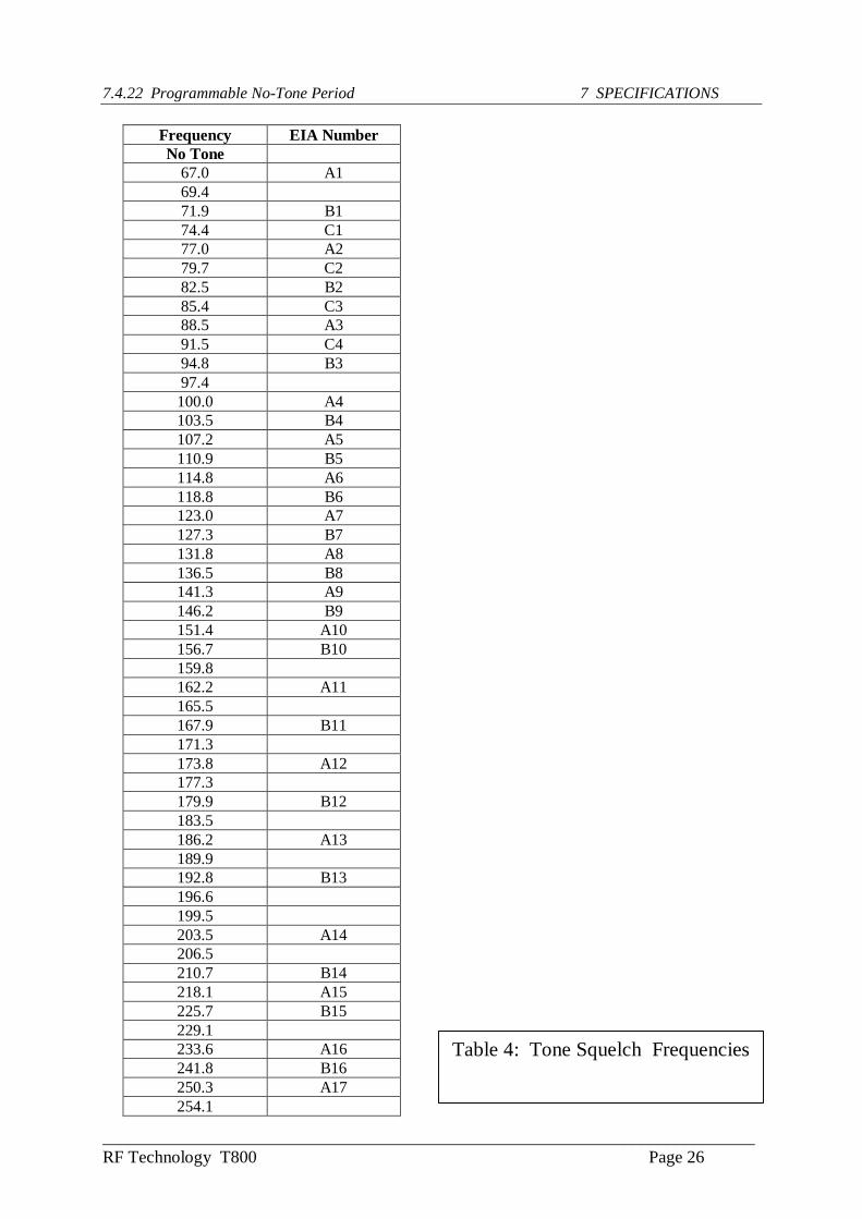
Tone frequencies are given in table 4.
7.5 Connectors
7.5.1 Antenna Connector
Type N Female Mounted on the module rear panel
_______________________3 The reverse phase burst is usually sufficient to eliminate squelch tail noise in higher-quality mobiles
___________________________________________________________________________RF Technology T800 Page 26
7.4.22 Programmable No-Tone Period 7 SPECIFICATIONS
Frequency EIA NumberNo Tone
67.0 A169.471.9 B174.4 C177.0 A279.7 C282.5 B285.4 C388.5 A391.5 C494.8 B397.4100.0 A4103.5 B4107.2 A5110.9 B5114.8 A6118.8 B6123.0 A7127.3 B7131.8 A8136.5 B8141.3 A9146.2 B9151.4 A10156.7 B10159.8162.2 A11165.5167.9 B11171.3173.8 A12177.3179.9 B12183.5186.2 A13189.9192.8 B13196.6199.5203.5 A14206.5210.7 B14218.1 A15225.7 B15229.1233.6 A16241.8 B16250.3 A17254.1
Table 4: Tone Squelch Frequencies

___________________________________________________________________________RF Technology T800 Page 27
7 SPECIFICATIONS 7.5.2 Power & I/O Connector
7.5.2 Power & I/O Connector
25-pin “D” Male Mounted on the rear panel
7.5.3 Test Connector
9-pin “D” Female mounted on the front panel


![Chapter 1 · RF field, including devices, circuits and packaging [1], such a technology had also been referred to RF MEMS technology. By using RF MEMS technology, the compact, low](https://static.fdocuments.net/doc/165x107/5f0308637e708231d40733e9/chapter-1-rf-field-including-devices-circuits-and-packaging-1-such-a-technology.jpg)