System Power Integrity Impact by Package Power ... - url.t Power... · Power/Ground Balls...
4
System Power Integrity Impact by Package Power/Ground Balls Assignment and Decoupling Capacitors Cheng-Hsun Lin#l, Chen-Chao Wang*2, Hung-Yu Wang #3 Department ofElectronic Engineering, National Kaohsiung Universi ofApplied Sciences, Kaohsiung 807, Taiwan '[email protected] '[email protected] * R&D Electrical Lab., Advanced Semiconductor Engineering, inc., Kaohsiung 811, Taiwan [email protected] Abstract- Power integrity is one of the important issues of system design. Power and current levels are expected to increase with a corresponding to decrease in the voltage and increment of I/O number. Based on these factors, system designer faces the challenge on power delivery network. The power/ground (P/G) ball is oſten used as a link between the package and printed circuit board (PCB). It relates to the system power distribution from the voltage regulator module (VRM) to Ie. When considering the power delivery network (PDN) design, power/ground balls position is the key point for complete power delivery. In this research, the assignment of the power/ground balls at different places and improvement of resonance impedance with different decoupling capacitors have been investigated for the impact of power integrity. The proposed arrangement of power/ground balls position is presented. The parasitic effects for different conditions of system design are extracted for comparison. The simulation results confirm with our theoretical analysis. 1. INTRODUCTION The shrinking of the device feature sizes and the increasing complexity of ICs require higher operating equencies with faster clock rates. The ball grid array (BGA) package becomes an important technology to shorten propagation delay of signal. The package is the interconnection between one die circuitry and another die or the printed circuit board (PCB). Its electrical nction includes signal transmission and power delivery, known as signal and power integrity. For the high-pin-count package, signal integrity and power integrity have become the critical challenges that must be treated carelly at the system level considering the parasitic effects of package and PCB [I]-[4]. The induced effects include ringing, crosstalk, ground bounce and other related issues. As devices scale and more transistors are integrated into a single IC continuously, power and cuent levels are expected to increase with a corresponding decrease in the voltage and increase in I/O number [5], [6]. It increases the importance of power integrity design. The ability to supply clean power to the transistor circuits becomes very critical. So the design of PDN received much attention. Simultaneous switching noise (SSN) and cavity resonances are major issues for power integrity. The interconnections have resistance and inductance in them, are used to establish this connection. The cuent flowing through these paths creates both a DC drop and time-varying fluctuation of the voltage across the power and ground terminals of the Ie. The voltage fluctuation across the power supply of the IC is called power supply noise, or SSN, since it occurs only during the switching of the transistors [6]. This issue can be improved by adding the decoupling capacitor. When the is unable to respond because of its high output impedance, the current should be supplied by an alteative source for maintaining the voltage. In other words, when the output impedance of the V exceeds the desired impedance, then an alteative approach is necessary to pull down the impedance. Decoupling capacitors perfo this nction. However, since ESL and ESR parasites of the decoupling capacitor affect high equency response, the power supply noise should be resolved by more power/ground plane. In this paper, the power integrity effect results om the power/ground balls and decoupling capacitors assignment and decoupling capacitors values are studied. In the BGA package, the number of power/ground balls is limited. Therefore, for worst PDN case consideration, only one available pair of power/ground balls is discussed in this paper. The power integrity effect is investigated by virtue of PDN equivalent circuit. IT. TEST STRUCTURE As shown in Fig. I(a). 81-pin 4cm x 4cm BGA package is electrically mounted on a test PCB of 10cm x 8cm through solder balls of 561u diameter. Fig. 1(b) shows the cross section of the test sample. The BGA package consists of four copper layers with a total substrate thickness of 420um. The inner two layers are ground and power layers with 180um spacing. A two layer PCB with substrate thickness 700um are the power and ground planes on the PCB [I]. 978-1-4577-1559-4/12/$26.00 ©2012 IEEE 265
Transcript of System Power Integrity Impact by Package Power ... - url.t Power... · Power/Ground Balls...
System Power Integrity Impact by Package
Power/Ground Balls Assignment and Decoupling
Capacitors Cheng-Hsun Lin#l, Chen-Chao Wang*2, Hung-Yu Wang #3
Department of Electronic Engineering, National Kaohsiung University of Applied Sciences,
Kaohsiung 807, Taiwan
'[email protected] *R&D Electrical Lab., Advanced Semiconductor Engineering, inc.,
Kaohsiung 811, Taiwan
Abstract- Power integrity is one of the important issues of
system design. Power and current levels are expected to increase
with a corresponding to decrease in the voltage and increment of
I/O number. Based on these factors, system designer faces the
challenge on power delivery network. The power/ground (P/G)
ball is often used as a link between the package and printed
circuit board (PCB). It relates to the system power distribution
from the voltage regulator module (VRM) to Ie. When
considering the power delivery network (PDN) design,
power/ground balls position is the key point for complete power
delivery. In this research, the assignment of the power/ground
balls at different places and improvement of resonance
impedance with different decoupling capacitors have been
investigated for the impact of power integrity. The proposed
arrangement of power/ground balls position is presented. The
parasitic effects for different conditions of system design are
extracted for comparison. The simulation results confirm with
our theoretical analysis.
1. INTRODUCTION The shrinking of the device feature sizes and the
increasing complexity of ICs require higher operating frequencies with faster clock rates. The ball grid array (BGA) package becomes an important technology to shorten propagation delay of signal. The package is the interconnection between one die circuitry and another die or the printed circuit board (PCB). Its electrical function includes signal transmission and power delivery, known as signal and power integrity. For the high-pin-count package, signal integrity and power integrity have become the critical challenges that must be treated carefully at the system level
considering the parasitic effects of package and PCB [I ]-[4]. The induced effects include ringing, crosstalk, ground bounce and other related issues. As devices scale and more transistors are integrated into a single IC continuously, power and current levels are expected to increase with a corresponding decrease in the voltage and increase in I/O number [5], [6]. It increases the importance of power integrity design. The ability to supply clean power to the transistor circuits becomes very critical. So the design of PDN received much attention.
Simultaneous switching noise (SSN) and cavity resonances are major issues for power integrity. The interconnections have resistance and inductance in them, are used to establish this connection. The current flowing through these paths creates both a DC drop and time-varying fluctuation of the voltage across the power and ground terminals of the Ie. The voltage fluctuation across the power supply of the IC is called power supply noise, or SSN, since it occurs only during the switching of the transistors [6]. This issue can be improved by adding the decoupling capacitor. When the VRM is unable to respond because of its high output impedance, the current should be supplied by an
alternative source for maintaining the voltage. In other words, when the output impedance of the VRM exceeds the desired impedance, then an alternative approach is necessary to pull down the impedance. Decoupling capacitors perform this function. However, since ESL and ESR parasites of the decoupling capacitor affect high frequency response, the power supply noise should be resolved by more power/ground plane.
In this paper, the power integrity effect results from the power/ground balls and decoupling capacitors assignment and decoupling capacitors values are studied. In the BGA package, the number of power/ground balls is limited. Therefore, for worst PDN case consideration, only one available pair of power/ground balls is discussed in this paper. The power integrity effect is investigated by virtue of PDN equivalent circuit.
IT. TEST STRUCTURE As shown in Fig. I (a). An 81-pin 4cm x 4cm BGA package
is electrically mounted on a test PCB of 10cm x 8cm through solder balls of 561 urn diameter. Fig. 1 (b) shows the cross section of the test sample. The BGA package consists of four copper layers with a total substrate thickness of 420um. The inner two layers are ground and power layers with 180um spacing. A two layer PCB with substrate thickness 700um are the power and ground planes on the PCB [I].
978-1-4577-1559-4/12/$26.00 ©2012 IEEE 265

The research has been execution by SI-wave simulation completely. The S-parameter of PCB and package has been measured respectively. The measured result of electrical properties is compared with simulation, as shown in Fig. 2. It can be observed that the measured and simulated results are consistent below 30Hz. The simulated result of the integrated structure with multiple power/ground balls connection in Fig. I is shown in Fig. 3. It can be observed that the simulated result of combined structure contains both PCB and package characteristics. This structure IS used In following investigation.
(a) (b)
Fig. I (a) Test sample structure. (b) Cross section of the test sample.
·20
'" -30 ..,
� -40
·50
-60
·70
0
·'0
·20 '" ..,
N -30 <h
"0
·50
11--1;0
2
Ireq, GHz (a)
freq, GHz
(b)
8 9
Measurement -
Smulatioo
10
5 9 10
Fig. 2 The measured and simulated results of (a) Package (b) PCB
TIT. EFFECT OF SYSTEM DESIGN
The interaction between the PCB and package include resistance, capacitance and inductance. The transient current flowing through an inductor causes voltage drop. A positive dl/dt through the inductor causes a voltage drop across it, resulting in a reduction in the supply voltage across the IC terminals and causing a performance problem due to a negative spike in the IC supply voltage. Similarly, a negative di/dt through the inductor increases the supply voltage across
the IC terminals, resulting in a positive spike, which causes reliability problems. It can be improved by reducing the current path on the PCB due to the lower inductance on package.
·10
·20
!g ·30
;::; CJ) ·40
·50
.70+-,--,-,,-.--,--,--,-,,-.--,--,--,-,,-.--,--rl
10
Ireq, GHz
Fig. 3 Simulation result of integrated test structure.
In the resonant circuit, capacitance and inductance change with frequency. The inductance interacts with the capacitance, causing it to resonate. The decoupling capacitors are capacitive below the resonant frequency and become inductive above the resonant frequency. The resonant circuit can cause a large anti-resonance in the impedance profile of IC. Large voltage fluctuations can occur if the operating frequency of the chip coincides with the chip-package antiresonance frequency [6]. To study the power integrity effect of package power/ground balls assignment and decoupling capacitors, various cases are considered as below.
(a) (b)
• Ground ball o Power ball • Port
Fig. 4 (a) Power/ground balls assignment on four corner. (b) Power/ground balls position assignment for the same distance.
TABLE I THE EQUIVALENT INDUCTANCE FOR DIFFERENT
POWER/GROUND BALLS POSITIONS
PIO ball location Equivalent inductance
Upper left 6.809nH
Upper right 6.001nH
Lower left 6.157nH
Lower right 5.893nH
A. Power/Ground Balls Assignment J
This case is setting measured portl as the VRM on the PCB lower-right position. Port2 is set as the power port of Ie.
266

Power/ground balls are assigned in the four corners of package between the package and PCB in turn. Let the power balls is close to the ground ball, as shown in Fig. 4(a). The four equivalent inductance data can be obtained from Sl-wave simulation result, as shown in Table 1. The better power/ground balls position is on lower-right, because the distance is shortest between portl and power/ground balls.
B. Power/Ground Balls Assignment 11
For power/ground balls assignment, the preferred design is a power ball in the vicinity of a ground ball. But it is not always feasible for practical design. The noise effect will be increased by longer distance between the power ball and
ground ball. For the cases in Fig. 4(b), the power ball and ground ball with identical distance and different position is considered. The three equivalent inductances are obtained from simulation, as shown in Table IT. The shortest current path is the ground ball in the vicinity of port2 due to its lower parasitic inductance on the package.
TABLE II THE EQUIVALENT INDUCTANCE FOR DIFFERENT GROUND BALLS
POSITIONS
G ball location G ball I G ball 2 G ball 3
(a)
• Ground ball o Powerb.n • Port
Equivalent inductance 7. I 67nH 7.611nH 7.515nH
(b)
eGroundball (., Power ball OCapacltor .POrl
Fig. 5 (a) Diflerent ground ball position. (b) System with decoupling
capacitor.
'" .. E ... N
aE 1 -.------�--------------------------_,
1E1
G ball 1 G ball 2 G ball 3 G ball 4 G ball 5
1 E-1 + ___ ......;� ______ ......::=======::::..j lEa 7E8
freq, Hz
Fig. 6 Simulation Z 11 of ground ball position.
C. Power/Ground Balls Assignment III
In the case of the fixed power ball, different ground ball locations on the package are considered, as shown in Fig. 5(a). Table TIT shows the five equivalent inductance data for different ground ball locations. Their system impedances ZII are given in Fig. 6. The ground ball I in Fig. 5(a) is the better choice since the package has lower unit equivalent inductance compared with PCB.
TABLE III THE EQUIVALENT INDUCTANCE FOR DIFFERENT GROUND BALLS
POSITIONS
G ball location Equivalent inductance G ball I 5.893nH G ball 2 6.415nH G ball 3 6.783nH G ball 4 7.028nH G ball 5 7.167nH
D. Decoupling Capacitors with Different Values It is known that the decoupling capacitor can be used to
lower the noise level. For fixed power/ground balls and decoupling capacitor locations, capacitors with different values are considered, as shown in Fig. 5(b). The system impedances Z21 for different decoupling capacitance are shown in Fig. 7.
'"
1 6 --r--------;;;1-�===:::;l .J m1
14
12
10
m4_10nF cap ----
m3_1nF cap ---- •• -.
m2_0.1nF cap ---
ml_bare
E 8 ... � 6
4 --=-==-::,,..,,. 2
O ����--.-�����--��� 1 E8 1 E9
freq. Hz
Fig. 7 Diflerent values decoupling capacitor simulation result.
As shown in Fig. 7, decoupling capacitor (ESL=OAnH, ESR=O.IO) alters the resonant impedance. If this resonant
impedance Z21 is less than the designed target impedance, the system power integrity will not be degraded. The choice of decoupling capacitor value depends on resonant impedance band. From Fig. 7, it can be observed that the InF decoupling capacitor attains the better noise effect to suppress the impedance of bare structure. The 10nF capacitor can be used to suppress resonant impedance on lower frequency band, but it causes the larger resonant impedance on 100 MHz.
267
'" .. E
C1
-Ground ball o Power ball o Capacitor .Port
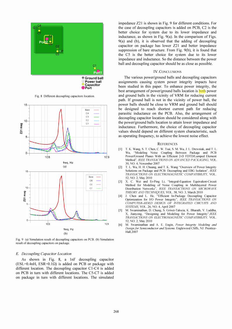
Fig. 8 Different decoupling capacitors location.
1 5 -.--------------------------------------.
10
1 E8
freq, Hz (a)
Bare
C4
C3
C2
C1
1E9
1 5-,-------------------------------------,
10
'" .. E
�
1E8
freq, Hz (b)
Bare -
jJ C6 -
C7 -
1E9
Fig. 9 (a) Simulation result of decoupling capacitors on PCB. (b) Simulation result of decoupling capacitors on package.
E. Decoupling Capacitor Location
As shown in Fig. 8, a InF decoupling capacitor (ESL=OAnH, ESR=O.I Q) is added on PCB or package with different location. The decoupling capacitor C l-C4 is added on PCB in turn with different locations. The C5-C7 is added on package in turn with different locations. The simulated
impedance Z21 is shown in Fig. 9 for different conditions. For the case of decoupling capacitors is added on PCB, C2 is the better choice for system due to its lower impedance and inductance, as shown in Fig. 9(a). In the comparison of Figs. 9(a) and (b), it is observed that the adding of decoupling capacitor on package has lower Z21 and better impedance suppression of bare structure. From Fig. 9(b), it is found that the C5 is the better choice for system due to its lower impedance and inductance. So the distance between the power ball and decoupling capacitor should be as close as possible.
IV. CONCLUSIONS
The various power/ground balls and decoupling capacitors
assignments causing system power integrity impacts have been studied in this paper. To enhance power integrity, the best arrangement of power/ground balls location is both power and ground balls in the vicinity of VRM for reducing current path. If ground ball is not in the vicinity of power ball, the power balls should be close to VRM and ground ball should be designed to reach shortest current path for reducing parasitic inductance on the PCB. Also, the arrangement of decoupling capacitor location should be considered along with the power/ground balls location to attain lower impedance and inductance. Furthermore, the choice of decoupling capacitor values should depend on different system characteristic, such as operating frequency, to achieve the lowest noise effect.
[1]
[2]
[3]
[4]
[5]
[6]
REFERENCES
T. K. Wang, S. T. Chen, C. w. Tsai, S. M. Wu, 1. L. Drewniak, and T. L. Wu, "Modeling Noise Coupling Between Package and PCB Power/Ground Planes With an Efficient 2-D FDTD/Lumped Element Method", IEEE TRANSACTIONS ON ADVANCED PACKAGING, VOL. 30, NO.4, November 2007 T. L. Wu, H. H. Chuang, and T. K. Wang "Overview of Power Integrity Solutions on Package and PCB: Decoupling and EBG Isolation", IEEE TRANSACTIONS ON ELECTROMAGNETIC COMPATIBILITY, VOL. 52, NO.2, May 2010 X. C. Wei and Er-Ping Li, "Integral-Equation Equivalent-Circuit Method for Modeling of Noise Coupling in Multilayered Power Distribution Networks", IEEE TRANSACTIONS ON MICROWAVE
THEORY AND TECHNIQUES, VOL. 58, NO.3, March 2010 J. Chen and L. He, "Efficient In-Package Decoupling Capacitor Optimization for I/O Power Integrity", IEEE TRANSACTIONS ON COMPUTER-AIDED DESIGN OF INTEGRATED CIRCUITS AND
SYSTEMS, VOL. 26, NO.4, April 2007 M. Swaminathan, D. Chung, S. Grivet-Talocia, K. Bharath, V. Laddha, X, Jianyong, "Designing and Modeling for Power Integrity",IEEE TRANSACTIONS ON ELECTROMAGNETIC COMPATIBILITY VOL. 52, NO.2, May 2010 M. Swaminathan and A. E. Engin, Power Integrity Modeling and Designfor Semiconductor and Systems. Englewood Cliffs, NJ: Prentice-Hall,2007
268
tyeh
底線
tyeh
螢光標示