PSoC® 63BL Family Datasheet, Programmable System-on-Chip ...
Upload
doannguyetCategory
view
226download
0
SYSTEM-ON-PROGRAMMABLE-CHIP DESIGN USING A UNIFIED DEVELOPMENT ENVIRONMENT
by
Nicholas Wieder
A thesis submitted to the faculty of The University of North Carolina at Charlotte
in partial fulfillment of the requirements for the degree of Master of Science in the
Department of Electrical and Computer Engineering
Charlotte
2007
Approved by: _____________________________ Dr. James M. Conrad _____________________________ Dr. Ivan L. Howitt _____________________________ Dr. Bharat S Joshi

ii
© 2007 Nicholas Wieder
ALL RIGHTS RESERVED

iii
ABSTRACT
Nicholas Wieder. System-On-Programmable-Chip Design Using a Unified Development Environment. (Under the direction of DR. JAMES M. CONRAD).
As embedded systems become increasingly complicated, the need for specialized
processing becomes greater as well. The System on a Programmable Chip (SoPC)
approach to creating these embedded systems involves using configurable architecture
available through Field Programmable Gate Arrays (FPGAs). The SoPC approach allows
designers to combine preexisting components to create a custom architecture for their
project.
This thesis illustrates one example of an SoPC design that combines existing and
custom components. This thesis also shows how using the Unified Development
Environment of Altium Designer aids in this process.

iv
ACKNOWLEDGEMENTS
Almost every major accomplishment of a single person is facilitated by the support of
many others, the successes of this thesis is no different. First, I would like to thank my
adviser Dr. James Conrad, for his support during this thesis, and opening my eyes to the
embedded world. Also, I would like to thank my boss and adviser Dr. Pat Gardner for his
support and encouragement, and all my coworkers for their understanding and flexibility,
during the last few years. Finally, I would like to thank my wife Kristy Wieder for
keeping me fat and happy, although we do not see each other as much as we would like,
her love keeps me going through the long hours.

v
TABLE OF CONTENTS
CHAPTER 1: INTRODUCTION 1
1.1 Previous Work 2
1.2 Importance 4
1.3 Thesis Organization 5
CHAPTER 2: SYSTEM ON A PROGRAMMABLE CHIP DESIGN 7
2.1 FPGAs 7
2.2 IP Cores 10
2.2.1 Types of IP Cores 11
2.2.2 Availability and Reuse 12
2.3 I/O selection 13
2.4 Bus selection 13
2.4.1 AMBA 13
2.4.2 CoreConnect 14
2.4.3 Wishbone 16
2.4.3.1 Wishbone Interconnections 17
2.4.3.2 Wishbone Interface 18
2.5 Verification and Test 22
CHAPTER 3: DEVELOPMENT 24
3.1 Hardware Design 24
3.1.1 Available Processors and Selection 27
3.1.1.1 Pipeline Architecture 28
3.1.1.2 Interrupts 29

vi
3.1.1.3 Processor Memory Organization 30
3.1.2 Peripheral Design 33
3.1.2.1 Wishbone Interconnect 33
3.1.2.2 Serial Communications 34
3.1.2.3 Display 35
3.1.3 Memory Design 36
3.1.3.1 RAM 36
3.1.3.2 Peak Detection 36
3.2 Software Design 38
3.2.1 HAL 39
3.2.2 Application Layer 40
3.2.3 Program Flow 40
CHAPTER 4: VERIFICATION\DEBUGGING 42
4.1 Hardware 42
4.2 Software 45
CHAPTER 5: SUMMARY 48
REFERENCES 50
APPENDIX A: HARDWARE DESIGN DOCUMENTS 54
Schematic: TopLevel.SchDoc 55
Schematic: Memory.SchDoc 56
Schematic: Peripherl.SchDoc 57
Schematic: TDisplay.SchDoc 58
Schematic: WB_GraphController.SchDoc 59

vii
VHDL File: PeakDet3.vhd 60
VHDL File: WB_LCD_Controller.vhd 63
APPENDIX B: SOFTWARE SOURCE 65
Source File(s): CRC16.c and CRC16.h 66
Source File(s): Datatype.h 69
Source File(s): EnvDataPacket.c and EnvDataPacket.h 70
Source File(s): FullScanPacket.c and FullScanPacket.h 73
Source File(s): HAL.h 75
Source File(s): hardware.h 76
Source File(s): ISR.c 77
Source File(s): LCDOut.c and LCDOut.h 78
Source File(s): Main.c 80
Source File(s): PowerControl.c and PowerControl.h 84
Source File(s): Que.c and Que.h 87
Source File(s): ReadingPacket.c and ReadingPacket.h 90
Source File(s): Sensor.c 92
Source File(s): TSK3000_Reg.c and TSK3000_Reg.h 97
Source File(s): uart16550A.c and uart16550a.h 102
Source File(s): WindowReader.c and WindowReader.h 108

viii
LIST OF FIGURES
Figure 2.1 Basic Layout of a FPGA.................................................................................... 8
Figure 2.2. Abstraction of a 2-LUT ................................................................................... 9
Figure 2.3. Productivity Gap [4] ...................................................................................... 10
Figure 2.4. Basic AMBA [9]............................................................................................ 14
Figure 2.5. Basic CoreConnect Architecture [9]. ............................................................ 15
Figure 2.6. Basic (Shared Bus) Wishbone Architecture [9]. ........................................... 16
Figure 2.7. Point to point Wishbone Interconnection [19] .............................................. 17
Figure 2.8. Wishbone Data Flow Interconnection [19] ................................................... 17
Figure 2.9. Wishbone Crossbar Switch Interconnection [19].......................................... 18
Figure 2.10. Single Wishbone Read cycle ....................................................................... 22
Figure 3.1. Top Level Diagram........................................................................................ 25
Figure 3.2. Changing processor Options.......................................................................... 26
Figure 3.3. Basic five-stage pipeline [21]........................................................................ 29
Figure 3.4. Memory Map................................................................................................. 31
Figure 3.5. Peripheral Control Schematic........................................................................ 32
Figure 3.6. Peripheral Core Configuration on the Wishbone Interconnect ..................... 34
Figure 3.7. Memory Control Schematic .......................................................................... 37
Figure 3.8. General Program Flow. ................................................................................. 41
Figure 4.1. WB_GraphControl.SchDoc........................................................................... 43
Figure 4.2. Logic Analyzer and Simulation Output......................................................... 44
Figure 4.3. Logic Analyzer view ..................................................................................... 45
Figure 4.4. Instrument Panel and Nexus Debugger ......................................................... 46

ix
Figure 5.1. Display Output............................................................................................... 49

x
LIST OF TABLES
Table 2-1. Wishbone signals used [19] [20]. ................................................................... 20
Table 3-1. TSK3000A Pipeline stage description [20].................................................... 29

xi
LIST OF ABBREVIATIONS
ACK Acknowledge
ADC Analog to Digital Converters
ADR Address Bus
AHB Advanced High Speed Bus
AMBA Advanced Micro-controller Bus Architecture
APB Advanced Peripheral Bus
ARM Advanced RISC Machine
ASIC Application Specific Intergraded Circuit
ASP Advanced System Bus
CAD Computer Added Design
CLB Configurable Logic Blocks
CLK Clock
CYC Cycle
DAT Data Bus
DCR Device Control Register (bus)
DMA Direct Memory Access
DSP Digital Signal Processor
DXP Design Explorer
ECG Electrocardiogram
EX Execute
FF Flip-Flop
FPGA Field Programmable Gate Array
HAL Hardware Abstraction Layer
HDL Hardware Description Language
ID Instruction Decode
IF Instruction Fetch
IO Input/Output
IP Intellectual Property
ISR Interrupt Service Routine
JTAG Joint Test Action Group
LAX Logic Analyzer
LCD Liquid Crystal Display
LUT Look Up Table
MA Mater A
MB Master B
MDU Multiply Divide Unit
MEM Memory Access

xii
OPB On-chip Peripheral Bus
OS Operating System
PC Program Counter
PC Personal Computer
PIO Parallel Input/Output
PLB Processor Local Bus
PLC Programmable Logic Controller
PPC Power Personal Computer
RAM Random Access Memory
RISC Reduced Instruction Set Computer
ROM Read Only Memory
RST Reset
SA Slave A
SB Slave B
SC Slave C
SEL Select
SoC System on Chip
SoPC System on a Programmable Chip
SoRC System-on-a-Reprogrammable Chip
SRAM Static Random Access Memory
STB Strobe
TSK3000A Tasking 3000A
UART Universal Asynchronous Receive Transmit
VGA Video Graphics Adapter
VHDL VHSIC Hardware Description Language
VHSIC Very High Speed Integrated Circuit
WB Register Write Back
WB Wishbone Bus
WE Write Enable
WinCE Windows Compact Edition

CHAPTER 1: INTRODUCTION
System on a Programmable Chip (SoPC) designs are becoming more common as
embedded computing solutions [11]. Some reasons for this are the constantly increasing
complexity of embedded systems and the decreasing time to market. It is becoming
increasingly difficult for hardware only or software only designs to meet the requirements
of system. Using a SoPC design approach allows the designer to take advantage of the
major benefits of both hardware and software based approaches in order to meet
requirements [3].
The use of programmable logic allows the system architect to make some changes to
the system, and allows design flaws to be easily fixed, without affecting the schedule or
the budget as greatly as a strictly hardware design. On the other hand, hardware based
designs can be specialized to more efficiently execute some operations [1]. SoPC designs
also allow flexibility in systems where the architecture is not finalized during the initial
portions of the design process [2].
Another reason SoPC designs are becoming more prevalent is that all peripherals
required may be custom designed, or copied from other designs, and can be included in
one chip [11]. Traditionally, this type of design would be called a System on Chip (SoC)
and the hardware implementation would be in an Application Specific Intergraded Circuit
(ASIC). However, the cost and risk associated with ASIC designs are avoided by the use
of a Field Programmable Gate Array (FPGA), used in SoPC design. SoC and SoPC
designs are very similar. Almost any digital design, which can be implemented through

2
schematic, netlist, or Hardware Description Language (HDL), can be implemented on
either substrate. However, a limitation of SoPCs is the limited ability to integrate analog
devices into the design.
Popular analog devices, for instance, Analog to Digital Converters (ADC), may
be included on special FPGAs called Platform FPGAs. Platform FPGAs contain many
other digital, analog, or mix signal devices. These are referred to as defused cores.
Defused cores range in size and complexity from block RAM to embedded processors.
An example of the defused core used in this thesis is the hardware multipliers and block
RAM contained on the Xilinx XCS1000 [27].
Along with defused cores, many proprietary and open source [13] designs, called
Intellectual Property (IP) cores, are available for use. IP cores are available in many
different stages of completeness, ranging from development to fully tested and warranted.
Chapter 2.2 gives a more complete explanation of IP cores.
Using a unified design environment during the design process, helps reduce the
possibility that components will not easily interface with each other. This is done by
standardizing the interfaces between on chip peripherals. Altium Designer, which was
used for this research, eases design by making most IP cores available with a Wishbone
bus interface. This bus is discussed in more detail later.
1.1 Previous Work
The design developed during the writing of this thesis may be used as a
replacement for the front-end portion of a chemical detector. The design constraints for
the detector require an interface to the sensor engine through serial communication, a
method of processing the data received from the sensor, and visual output.

3
The design is derived from a project currently under development, implemented in
C++, as an application running on a Windows Compact Edition Operating System (OS).
One major issue with the current design is the amount of time spent finding peaks once
the data has been collected.
This project sets up the framework for a system that can read a sensor over RS-232,
store the data, perform peak detection in hardware, and then display the results.
Although the peak detection method is important, to ensure proper classification, it is not
the focus of this thesis. A second group at the University of North Carolina at Charlotte
is researching this topic in parallel.
A major design change from the current implementation is the lack of an OS. For
this project, the benefits of an OS are not significant enough to warrant the effort or
processing overhead required. The current implementation uses C++, however because
of its considerable overhead compared to C, most embedded processor compilers do not
support C++. Therefore, a majority of the current implementation was not reusable.
Numerous works based on SoC or SoPC designs have previously been presented,
most of these focus on the design process using tools supplied from FPGA manufactures,
Xilinx and Altera. Most of these designs like [17] use platform FPGAs with defused
microprocessor cores. In these designs, the debugging of the operating system is not
considered, so the majority of the debugging capabilities available are through an
embedded operating system.
Other works, which are more closely related to this thesis, detail SoPCs using
embedded processor cores that feature on chip debugging. One such work is [24], which
discusses the design of a SoPC based Programmable Logic Controller (PLC). This

4
design uses an Altera FPGA and their Nios embedded processor to implement the control
and communications required in a PLC.
Another project closely related to this thesis, but also utilizes a higher performance
system is presented by Al Khatib [17]. Al Khatib’s design puts two Digital Signal
Processor (DSP) cores on a single SoC in order to accurately track the variances in a
human heartbeat through an electrocardiogram (ECG). The work is closely related to this
thesis for both its use of embedded IP cores and for its requirement to do peak detection
on an input signal. However, the similarities end there. The real time requirements of
the system posed in [17] are much greater therefore, a higher end and expensive design is
chosen. In addition, the peak detection that is implemented in [17] is appropriate given
that the signal to be detected has a consistent shape and large signal to noise ratio; these
are not the case for this thesis.
1.2 Importance
According to United States government’s information on exposure to Sarin Nerve
Gas [26], during the first Gulf War, exposure to detectible concentration of sarin for 34
seconds can cause death, with side effects starting after only one second. The fact that a
faster detection of a dangerous chemical can save lives is one of the most important
reasons this thesis is important. Although this thesis does not go into complete detail of
the chemical detection process or the workings of the sensor, it is important to consider
the basics of detection, chemical detection.
To identify a particular agent with confidence, very often multiple peaks must be
present or absent. The combinations of these peaks determine the type of chemical

5
present. The operation of the sensor is a serial process, therefore accelerating each peak
detection can save seconds in the total process.
Another important characteristic of migrating the current implementation into an
SoPC is the possibility to, in the future, move the control portion of the sensor into a
single chip. As discussed previously, this thesis poses an alternate general system design
for only the peak detection and display portions of this design. However, this is no
reason to expect that the entire control portion of the system could not be implemented in
an SoPC design given the proper time and resources. Another advantage of this design is
possible battery savings if the two boards are combined in a single SoPC design. The
current design uses a DSP and a general-purpose embedded processor, running the
operating system for the front end.
1.3 Thesis Organization
This thesis is organized such that background information required in each chapter
is presented in the previous chapters. The intent is that someone with little knowledge of
the subject should be able to read and understand the information presented.
Chapter 2 presents some basics of SoPC design. This chapter provides a background
in IP cores, compares the major bus architectures in use, and discusses some terminology
used during design and verification.
Chapter 3 discusses the design decisions made during development. The first sub
section discusses the hardware design phase of the thesis, including processor choice,
peripheral design and design layout. The second subsection discusses the software
design, including abstraction layers and program flow.

6
Chapter 4 presents the tools and methods used for debugging both the hardware and
software portions, and their interdependences.
The summary of the results is detailed in Chapter 5 followed by the references in
Chapter 6.

CHAPTER 2: SYSTEM ON A PROGRAMMABLE CHIP DESIGN
The Xilinx Design for reuse methodology [14] discusses the shift from SoC to
SoPC, although they use the term System-on-a-Reprogrammable Chip (SoRC). This
manual defines SoRC as the grouping of an entire system on a single, programmable,
chip. The SoRC design normally contains some kind of computation engine, user
defined logic and on chip memory, all connected through a system level integration
method. The following subsections give detail of these elements.
2.1 FPGAs
The FPGA is the substrate on which an SoPC design is implemented. Basically an
FPGA is an integrated circuit which contains configurable memory blocks, allowing the
designer to implement a logic or system design [15].
Figure 2.1 shows the basic layout of an FPGA. The Configurable Logic Blocks
(CLB) are located in rows and columns. The routing network shown connects one CLB
to the next in order to form the desired logic. Each CLB contains smaller blocks, Flip-
Flops (FF) and Look up Tables (LUT). The CLB also contains some internal routing in
order to connect the Flip-Flops and LUTs required. Flip-Flops are used to store
information from one clock cycle to the next and are required for some but not all
operations. LUTs are programmable memory blocks. These LUTs are normally
programmed prior to run time with the desired outputs based on the inputs. Figure 2.2
depicts the operation of a two input LUT, or 2-LUT. All LUTs will only have one
possible output, but the number of inputs (n) determines the total amount of combinations

8
possible, which is 2n, and is equal to the amount of memory required for each LUT. In
Figure 2.2, the 2-LUT will have 22 = 4 possible combinations. Although the example
shown is a 2-LUT, typically, FPGAs use 4-LUTs, but this may vary between
manufactures [15].
Switch Box
Connect
Box
CLB
LUT
LUT
FF
FF
Switch Box
Connect
Box
CLB
LUT
LUT
FF
FF
Switch Box
Connect
Box
CLB
LUT
LUT
FF
FF
Switch Box
Connect
Box
CLB
LUT
LUT
FF
FF
Connect
Box
CLB
LUT
LUT
FF
FF
Connect
Box
CLB
LUT
LUT
FF
FF
CLB
LUT
LUT
FF
FF
CLB
LUT
LUT
FF
FF
CLB
LUT
LUT
FF
FF
Figure 2.1 Basic Layout of a FPGA
The configuration of an FPGA is generally an automated process, Computer Added
Design (CAD) tools convert input schematic, netlist , or HDL designs into a bit stream
which is then used to program the connection/configuration and memory blocks of the
FPGA. There are four basic steps required for CAD tools to create the configuration file,
or bit stream, needed to implement the design on an FPGA:

9
1. Synthesis, during this step the user's input design is converted to low level
logic gates which are used by the second step.
2. Mapping, since the number of FFs and the size LUTs varies between chips
and manufactures, mapping is an important step that builds up the
configuration for each CLB, based on the chip selected. Mapping decides
what logic should be combined into a CLB.
3. Place and Route determines which CLB the logic is placed. Place and
Route also determines the configuration of the connect and switch boxes.
4. The final Step is to convert the configuration information into a bit stream
that can be downloaded into the FPGA.
Figure 2.2. Abstraction of a 2-LUT

10
2.2 IP Cores
The semiconductor industry continues to increase the number of transistors per
chip, keeping pace with Moore’s law. Moore’s law states that the numbers of transistors
on a chip will double every 18–24 months [6]. This constant increase creates a challenge
for designers to find ways to decrease the productivity gap [4]. The productivity gap is
the distance between the two lines shown on Figure 2.3. The top line represents the
increasing complexity and capability of the hardware, while the lower line illustrates
designer productivity. One method used to fill this gap is to reuse components. Many
times these components are custom designs that make each product unique; however,
most components needed have been previously designed. These existing components
may include memory, embedded processors, standard input/output (IO) devices, and
other logic devices [7]. These components, which can be custom designed or existing,
are often called IP cores.
Figure 2.3. Productivity Gap [4]

11
IP cores used in SoC designs may be either mixed signal or completely digital
logic devices. Mixed signal cores can include radios, analog to digital converter, digital
to analog converters, and many more devices [5]. Mixed signal cores may be included in
SoC designs since they specify ASIC designs; however, SoPC designs run on existing
hardware and can only include mixed signal cores when included in a platform-based
design. The most common IP cores used in SoPC design are digital cores. These cores
include, but are not limited to, implementation of IO devices, signal encoding, embedded
processors, and custom logic.
2.2.1 Types of IP Cores
According to the Reuse Reference Manuel, which lays out guidelines for the
industry, the three main types of IP cores are hard, firm, and soft [7].
Hard IP cores are optimized for their application and normally are guaranteed
from the provider. This type of core reduces risk since they have been built and tested,
however they are less portable and more expensive than other types. Until recently, the
majority of cores available were hard cores. A good example of this is the Advanced
RISC (Reduced Instruction Set Computer) Machine (ARM) line of processors that are
only available from the design house in the form of a hard IP core [12].
A small percentage of the IP core market is available in the form of firm IP.
These blocks offer similar reliability benefits of hard IP, however they are parameterized,
meaning designers can specify aspects of the core to fit more applications and hardware
platforms [4].
The majority of cores used in SoPC designs are soft IP. These cores are useful to
digital designers since they often come in the form of modifiable HDL. This form of IP

12
does not come with the guarantees of the others, since the hardware can be changed and
will be laid out differently each time. Often soft IP will come in an encrypted form
making it extremely difficult to modify, but allowing the other benefits of soft cores [4].
2.2.2 Availability and Reuse
The most common source for IP cores, in a company is existing designs. This
type of reuse may allow designers to reduce design risk by using familiar cores.
However, often because of other concerns, this may be the least dependable source.
Typically, designs must be completed in a short time to reduce the time to market or to
keep a project on time and under budget. However, to create reusable IP, the design
process will generally take additional weeks to complete [8]. Internally designed cores
will, and should, play a large part in designs, but the design process must take a “design
for reuse” approach in order for the reuse to pay off [8].
IP cores are also available from many third party vendors and open source
projects on the Internet. The most common may come as individual cores or as packages
like Xilinx Embedded Development Kit. Altium Designer also comes with a set of IP
cores. Using prepackaged cores may increase productivity by ensuring they will work
together, providing a common network architecture, and reducing research and
procurement time for each core. Although the designer’s productivity may be increased
and risk reduced by using pre packaged cores, the system’s performance may not be
optimal. Prepackaged cores are designed for general use; designs specialized for
individual applications can offer improvements such as speed or size.

13
2.3 I/O selection
During normal development of an embedded system, the decision of what types
of device I/O are required must be made early, often the ideal processor cannot be used
because it does not support the correct or enough device I/O. This is not a problem when
designing a device using an SoPC as the main processing component. In this case, the
designer may include all the required I/O options to include most types of I/O ports, or
including custom I/O. When platform FPGAs are used, they may contain defused IP,
using these IP blocks is advantageous, however extra IP can be added beyond the defused
blocks.
2.4 Bus selection
Communications between different portions of a system are standardized by
attaching each component to a bus. A bus is a set of wires, which are shared by 2 or
more components. Most buses have one device that controls the communication, called
the master, and other devices that respond to commands sent from the master, called
slaves. Some buses are specialized for certain applications, for example, accessing
memory, and others are more generic and suitable for use by many peripherals.
The following subsections provide an overview of the three main bus standards
used. Many other bus architectures like in [23] have been purposed, however, using a
standard architecture increases the number of IP cores available. All of these standards
have the same basic goal, which is to easily connect IP cores.
2.4.1 AMBA
ARM’s Advanced Micro-controller Bus Architecture (AMBA) is actually a
collection of buses. The two buses that are intended to connect the processor are the

14
Advanced High Speed Bus (AHB) and the Advanced System Bus (ASP). Both of these
buses are intended to communicate to high speed peripherals like Direct Memory Access
(DMA) controllers, and include an Arbiter, which controls access to the bus. The slower
devices like a Universal Asynchronous Receive Transmit (UART) or a parallel
input/output (PIO) are located on a second bus called the Advanced Peripheral Bus
(APB).
Figure 2.4. Basic AMBA [9].
2.4.2 CoreConnect
In Figure 2.4, the basic architecture of AMBA is illustrated. This figure shows
that any communication between the AHB/ASP and slower peripherals, located on the
APB, are accomplished through a bridge. The purpose of the bridge is to allow the

15
AHB/ASP to continue to operate at its maximum speed but still communicate to slower
devices.
Figure 2.5. Basic CoreConnect Architecture [9].
IBM created CoreConnect to interface with their Power PC (PPC) line of
embedded processors, with the intent to provide the highest performance possible.
Although CoreConnect was designed for use with the PPC, any processors designed with
the correct interface may use it. As with AMBA, CoreConnect is actually a combination
of multiple buses. The main interface to the processor is through the Processor Local Bus
(PLB). This is the standard interface to high-speed peripherals and provides the
processor access to slower peripherals through a bridge. Communication between cores
on the PLB that involve smaller amounts of data can dramatically decrease the

16
performance of the PLB. To overcome this, these devices are also connected to the
Device Control Register (DCR) bus.
Slower cores like UARTs and keyboard interfaces are connected to the On-chip
Peripheral Bus (OPB). Communication between the OPB and the PLB is done through
bridges [10].
Figure 2.5 illustrates the basic architecture of the CoreConnect. It should be
noted that it is very similar to AMBA, with the addition of the DRC.
Figure 2.6. Basic (Shared Bus) Wishbone Architecture [9].
2.4.3 Wishbone
The Wishbone Bus architecture, shown in Figure 2.6, can be much simpler than
CoreConnect or AMBA. The Wishbone standard was originally developed by Silicore
Corp., but is now maintained by Opencores.org [13], a website for developers of open
source cores to post and download designs. The major difference between CoreConnect
and AMBA is that the Wishbone architecture includes only a high-speed bus. However
many designs, such as the one used in this thesis, include two Wishbone buses, one for

17
high-speed peripherals like memory and a second for slower devices. Since the
Wishbone bus is used in this thesis, the following sub sections give more detail on its
operation.
2.4.3.1 Wishbone Interconnections
There are four basic types of Wishbone interconnections: shared bus (shown
above), point-to-point, data flow, and crossbar switch [19]. As the name indicates, the
point-to-point , shown in Figure 2.7, interconnection allows two cores to talk to each
other. This is the simplest implementation, with one master and one the slave.
Figure 2.7. Point to point Wishbone Interconnection [19]
The Data flow Interconnection is a more complicated option, because each core in
the system acts as both a master and slave. This type of connection allows work to be
parallelized between the cores, possibly improving the performance of the system.
Figure 2.8. Wishbone Data Flow Interconnection [19]

18
The final type interconnection used in the Wishbone standard is the crossbar
switch, shown in Figure 2.9. This interconnection allows a system to include multiple
masters and multiple slaves. The Wishbone interconnect determines the routing required
to connect each master to the requested slave device.
Figure 2.9. Wishbone Crossbar Switch Interconnection [19]
2.4.3.2 Wishbone Interface
19
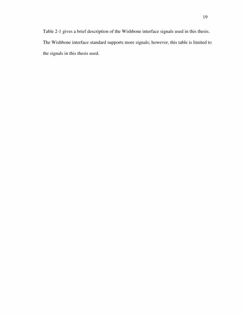
Table 2-1 gives a brief description of the Wishbone interface signals used in this thesis.
The Wishbone interface standard supports more signals; however, this table is limited to
the signals in this thesis used.

20
Table 2-1. Wishbone signals used [19] [20].
Name Symbol Output Of Description
Acknowledge ACK Slave Set by the slave to acknowledge the start
of the cycle, cleared by the slave to
indicate the completion of the cycle.
Clearing this bit informs the master that
output data is valid, for a read cycle.
During write cycle operation, clearing
this bit may have different meanings for
each core, however, at a minimum, this
informs the master that the input data has
been read and will be processed.
Address Bus ADR[] Master The binary output of this bus determines
which core is used and any commands
sent to the core. The bus width can vary
depending on the attached cores and the
requirements of the system.
Clock CLK Master/System The clock rate may be set by the master
or the system clock.
Cycle CYC Master The cycle bit is set by the master to
indicate the start of a cycle and remains
high until the end of the cycle.

21
Name Symbol Output Of Description
Data Bus DAT[] Master/Slave The master and slave each have an input
and output bus. The bus width can vary
depending on the attached cores and the
requirements of the system.
Reset RST Master/System The reset signal may be asserted by the
master from the global system reset.
Select SEL Master The select signal is used to extend the
addressing from words to bytes.
Strobe STB Master This signal is set by the master at the
beginning of a cycle and cleared after
acknowledgement from the slave.
Write Enable WE Master The masters signal to the slave that it is
clear to write the output data.
A slave core can be read from in two methods; single and multiple reads. Figure
2.10 shows a single read from the masters’ point of view. The cycle is initiated when
both the STB_O and CYC_O are set. At the same point, the master clears the WE_O to
indicate a read cycle, and sets data to ADR_O and SEL_O, if needed. When the slave
core begins to process the data, it sets the ACK_I, places the output data on DAT_I, then
clears ACK_I. To end the single read cycle, the master reads the data on DAT_I and
clears both STB_O and CYC_O. In the case of a multiple read, the cycle would be the

22
same with one exception, CYC_O would not be cleared until all data was read. STB_O
would continue to cycle with each read as an acknowledgement to the slave.
Figure 2.10. Single Wishbone Read cycle
2.5 Verification and Test
Verification of a design is the process of determining if the design has correct
functionality prior to implementing it on the platform [28]. When designing a system
that is made from existing cores, much of the verification is performed by the core
vendors. The design of custom cores should be verified using simulation, to ensure the
interface and results are as expected.

23
Software portions of the project may also be verified by simulation or by running
them on a development machine, also known as the host. Running on a host system can
verify the operation of the portions of the software that are not hardware dependent.
Aspects like timing and some interfaces must be verified through simulation or held for
testing on the target.
For this work, testing is described as verifying inputs and outputs of the system
running on the target environment.

CHAPTER 3: DEVELOPMENT
3.1 Hardware Design
As described in Chapter 2.4.3, the main communications interface in this design is
the Wishbone Bus. The decision to use this interface was made early in the process
because of the abundance of peripherals made available through Altium Designer.
Although most peripherals are available in non-Wishbone variant, using the bus greatly
reduced the complexity of the processor code and simplified the hardware interface
design.
The schematic shown in Figure 3.1 has three main components. First, in the center
is the processor. The two green blocks represent other schematics. The schematic on the
left contains all logic, which resides on the peripheral bus and on the right the Memory
bus. Altium Designer requires all connections external to the FPGA to be located on the
top level schematic, therefore the serial port, Video Graphics Adapter (VGA) connection,
and Random Access Memory (RAM), are also located on this schematic. Each of these
schematics has many input and output ports. These are represented by the yellow arrows,
the direction of these ports, input or output, determines which way the arrow points, into
or out of the symbol.
The schematic symbol of the processor shown is typical of the 32-bit processors
available in Altium Designer; that is all 32-bit processors available contain a Wishbone
wrapper. This feature enables processors to be changed, at the hardware level, simply by

25
Figure 3.1. Top Level Diagram

26
right clicking on the processor and selecting a different type. This is shown in the drop
down box of Figure 3.2. This feature would come in handy if the target FPGA were
changed, for instance to a Xilinx Vertex II Pro, a platform FPGA containing a PPC [18].
This type of change would reduce the number of LUTs used on the chip by using the
defused core and may improve performance. The benefits and drawbacks of such an
approach are described later in Chapter 3.1.1, however the main reason the Tasking
3000A (TSK3000A) was chosen is to keep this design portable to any FPGA.
Figure 3.2. Changing processor Options.
Figure 3.2 also shows the configuration options available for the processors. The
first option is the amount of internal memory available. The benefit of this selection is
the ability to use as few block RAM elements as possible to implement the processors
software. The next option determines where multiplication is carried out, either emulated

27
by the complier or actually carried out on the processor. Selecting the hardware Multiply
Divide Unit (MDU) results in faster operation, but with greater physical resource usage.
The final two options are used for debugging. Disabling the Joint Test Action
Group (JTAG) debug port would reduce the processor size, but would also remove the
ability to debug software problems. The design used in this thesis is not large enough to
require the restriction of the internal memory, MDU, or JTAG; therefore the options
selected are optimized for speed and ease of use.
3.1.1 Available Processors and Selection
Altium designer comes with a large number of processors ranging from 8-bit
processors like the 8051 to the 32-bit Power PC (PPC405A). Some of the higher end
processors, the PPC405A, MicroBlaze, ARM 7 and Nios II, are hardware specific and
could not be used on the evaluation board used for this thesis. However, because of the
Wishbone wrapper which encapsulates all of these processors, if the design were
migrated to one of these processors, the hardware change would consist of changing the
selection in the drop down box shown in Figure 3.2.
As mentioned previously, the availability of numerous Wishbone-compliant cores
supplied with Altium made the decision to use this interface a simple one, however it did
not narrow the choice of processors. The decision did remove many of the 8-bit
processors except the TSK165 that also includes the Wishbone wrapper. Four main
factors supported the final decision to use the TSK3000A. First was the abundance of
example code, second, the possibility to more easily transition to a platform FPGA, third
the optional hardware MDU, and fourth is an option that has been advertised, but not yet
implemented. In Spring of 2006, at the Embedded Systems Conference, Altium

28
demonstrated Designer’s ability to easily convert C code to HDL [30]. Although it is
almost guaranteed not to execute as fast as hand coded HDL, it could, if implemented,
improve processing time with little to no effect on design time, compared to the strictly
software design. This feature was advertised in Spring 2006 however, it has not yet been
released to consumers.
3.1.1.1 Pipeline Architecture
The TSK3000A is a 32-bit Reduced Instruction Set Computer (RISC) processor.
This type of processor was introduced in the early 1980s and has seen considerable
changes since then. One feature of RISC processors is that instructions are executed in a
five-stage pipeline architecture. A five-stage pipeline means portions of five instructions
are loaded at one time, each of these instructions are broken into logical steps called
stages, described in Table 3-1.
In Figure 3.3, each row represents a new instruction, with the current processor
cycle highlighted in green. This figure shows that as one instruction is starting, others are
finishing. For most instruction types, this is acceptable; however, there are some
instruction types, for instance a branch, which disrupt this flow. When a branch
instruction is executed, in the Execute (EX) stage, the next instruction following the
branch is executed as well, prior to moving to the new location. This allows the
TSK3000A to only waste one instruction in the pipeline [20].

29
Table 3-1. TSK3000A Pipeline stage description [20]
Instruction Fetch (IF) The address stored in the Program Counter
(PC) is used to retrieve the next instruction
from memory.
Instruction Decode (ID) Required information is retrieved from
registers.
Execute (EX) Depending on the instruction type,
calculations are performed, and the PC is
updated
Memory Access (MEM), During load or store instructions, the output
data is read or written.
Register Write Back (WB) The results from the EX or MEM stages
are written to general purpose registers.
Figure 3.3. Basic five-stage pipeline [21]
3.1.1.2 Interrupts
The processor contains 32 configurable hardware exceptions called interrupts and
one internal timer interrupt. Each of the hardware interrupts has four possible situations

30
when an interrupt will be generated: low level, high level, falling edge, or rising edge.
The initial configuration of these interrupts takes place at the hardware level through the
schematic editor when configuring the Wishbone Interconnect, a core that is detailed in
later Chapters. The hardware and software are linked through the automatic generation
of “hardware.h” when using C source, as was for this thesis, or “hardware.asm” for an
assembly project.
During the software configuration of the interrupts, the selection must be made
for standard or vectored interrupts. In standard interrupt mode, every interrupt calls the
same function that in turn determines the priority of the current interrupts and executes
the required functions. In vectored interrupt mode, each interrupt has a dedicated handler
that is called. The priority of this vectored interrupts are based on the interrupt number,
with zero being the highest.
As will be discussed in Chapter 3.1.2 the TSK3000A communicates to peripheral
cores through the Wishbone interface, however since the processor acts as a master on
this bus, cores that wish to talk to the master must be polled for their status or signal an
interrupt when data is ready.
3.1.1.3 Processor Memory Organization
The TSK300A has dedicated ranges of memory reserved for external memory and
peripherals. Any read or writes to these memory locations are directed to the
corresponding Wishbone port. From the embedded software’s point of view, when a call
to an external device is made the processor handles all necessary Wishbone interface
actions to read or write to the intended device. Figure 3.4 shows the memory mapping
for this thesis. This figure shows the memory areas which may be mapped to peripherals,

31
external memory, and internal memory, on the left. On the right, the peripherals and
external memory which are actually mapped into this area are shown.
Figure 3.4. Memory Map
Mapping of the peripherals and external memory, and their corresponding
memory addresses, shown on Figure 3.4 was made easy by using the Wishbone
Interfaces of the Peripheral and Memory Control Schematics that will be discussed
further in Chapters 3.1.2 and 3.1.3. These devices were imported on the schematic view
of the processor, however, if the Wishbone interface was not used, or if individual
memory partitions were required, they could be specified through the processor
configuration menu. To incorporate the hardware design into the embedded

32
Figure 3.5. Peripheral Control Schematic.

33
software project, as discussed in Chapter 3.1.1.2 on interrupts, the memory addresses are
also added to “hardware.h” or “hardware.asm.”
3.1.2 Peripheral Design
The Peripheral Control portion of this design contains three major sections,
Wishbone interconnect, serial and display. A general overview of Figure 3.5 shows that
the serial connection is a uart16550 core, the display portion of the design consists of
U_DispCtrl, U_GphCtrl, and U_DisplayCtr, and these are all linked together using the
Wishbone interconnect. These portions of the design are discussed in greater detail in the
following sub sections.
3.1.2.1 Wishbone Interconnect
The peripheral cores, shown on Figure 3.5, are all attached to the Wishbone
interconnect. This component is the main interface with the processor. It handles the
routing of instructions, seen as simple memory reads and writes from the embedded
software. As discussed in Chapter 3.1.3, any memory reads or writes performed on
addresses 0xFF00000 to 0xFFFFFFFF are directed to the peripheral ports of the
processor. These instructions are further decoded and forwarded to their intended
peripheral. Setting up this decoding is accomplished through the schematic view of
Altium Designer, and is shown in Figure 3.6. The configure window of Figure 3.6 shows
the summary of the attached peripherals and their properties. The order peripherals listed
on this view determines the order they will appear on the schematic symbol. Selecting
Add or Edit Device on this window will bring up a more detailed dialog box, shown in
Device Properties, which allows modification of the properties shown in the summary
window.

34
Figure 3.6. Peripheral Core Configuration on the Wishbone Interconnect
3.1.2.2 Serial Communications
Originally, serial communication was accomplished by use of the WB_UART8
core, an implementation of a UART. However, after much time was spent attempting to
implement the driver, the effort was abandoned. There appeared to be some flaw in
either the core implementation or the documentation supplied. The core would only
signal the receive interrupt while it was also transmitting.
As an alternate solution, the uart16550 from opencores.org [13] was chosen. This
core is a soft IP core, available in the HDL Verilog. Integrating this core and
implementing the driver did not take much time at all. Two main advantages accelerated

35
the implementation of the drive, first was correct documentation of the registers. Second,
was the fact that the HDL was available for reference while debugging the driver code.
The only problem seen during the implementation was the repeat of data sent to the video
port. To determine the solution to this problem the UART core code was examined.
From this examination, it was noted that the uart16550 does not do any address decoding,
except to determine which register is being reference. Therefore, the Wishbone
interconnect must only forward information to the uart16550 when it is intended for this
core.
3.1.2.3 Display
The display requirements of this project did not dictate that a VGA output be
used, however the availability of the VGA, and lack of a simpler Liquid Crystal Display
(LCD) forced the use of the VGA output. Use of the VGA output also allowed the
addition of the graph display. The feature, which consumed relatively little design time,
eased debugging during the hardware/software integration.
The component U_TDisplay, which is an instantiation of TDisplay.SchDoc is
modified from a reference design provide with Altium Designer. The original design
included only the LCD display and required modification to include the graph output.
Control of the LCD display is handled through U_DisplayCtrl, an instantiation of
a VHSIC (Very High Speed Integrated Circuit) Hardware Description Language (VHDL)
document called WB_LCD_Controller.vhd. This design is also derived from a reference
design, the main functionality and interface to the TDispay.SchDoc remained the same.
However, the implementation was modified to enable communication over the Wishbone
bus.

36
The final core used in the peripheral design is the U_GphCtrl, an instantiation of
the schematic document WB_GraphControler.SchDoc. This design, used with the
Wishbone Interconnect, allows synchronous one-way communication from the processor
to the graph display.
3.1.3 Memory Design
During design of the memory control, a dual master approach to the external
RAM was created. This design allows the peak detector and the processor to access the
same memory space using the Wishbone bus. As with the peripheral control bus, the
communication from the processor is routed through a Wishbone Interconnect.
3.1.3.1 RAM
A major difference between this bus and the peripheral bus is the addition of the
Wishbone Dual Master, shown in Figure 3.7. The Dual Master allows the two
components to access the same core, in this case the SD Controller, a instance the of
WB_MEM_CTRL configured for two static RAM (SRAM) chips [29].
The Dual Master is configurable to suit almost any 8, 16, and 32-bit wide memory
buses and any address width from 0 to 32-bits. The priority given to each master is also
configurable. Currently the Dual Master is configured to using a first come first serve
priority called Round Robin, but could be configured to a preemptive scheme giving
either precedence [31].
3.1.3.2 Peak Detection
As mentioned in the introduction to this thesis, the peak detection algorithm is not
the focus and therefore a simple implementation has been created. From an interface

37
Figure 3.7. Memory Control Schematic

38
point of view, the peak detector is a Wishbone slave to the processor and a Wishbone
master to the SRAM.
The current implementation does not utilize the Wishbone master portion in order
to access the SRAM, therefore the values for each data set must be written directly to the
core. When a new value is written, the core compares it to the previous largest value and,
if greater, stores this value and its corresponding index.
The core has four commands. First is to reset the core; when this command is
received, the greatest point and its index are cleared. The second command is to receive
data; this data is passed in on the DAT_I line of the core along with the command and is
immediately compared to the previous data. The final commands are to retrieve the
greatest point and its location, which are passed back on the DAT_O lines of the core.
3.2 Software Design
The software used in the implementation of this thesis is a combination of reused,
derived and custom code. Reused code came with Altium Designer as parts existing
from example projects. Derived code came from multiple sources. The first was from
example projects. Much of the derived code started out as C++. This code is mainly
used to determine the validly of the information sent from the sensor. This code has
changed dramatically from the original C++ into the C used in this project. Finally,
custom code is used to link all others together. Included in this is code generated by the
development environment in order to link the hardware and software portions of the
project.
39
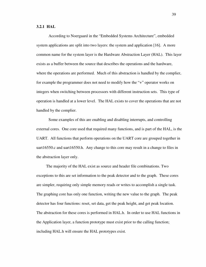
3.2.1 HAL
According to Noergaard in the “Embedded Systems Architecture”, embedded
system applications are split into two layers: the system and application [16]. A more
common name for the system layer is the Hardware Abstraction Layer (HAL). This layer
exists as a buffer between the source that describes the operations and the hardware,
where the operations are performed. Much of this abstraction is handled by the complier,
for example the programmer does not need to modify how the “+” operator works on
integers when switching between processors with different instruction sets. This type of
operation is handled at a lower level. The HAL exists to cover the operations that are not
handled by the complier.
Some examples of this are enabling and disabling interrupts, and controlling
external cores. One core used that required many functions, and is part of the HAL, is the
UART. All functions that perform operations on the UART core are grouped together in
uart16550.c and uart16550.h. Any change to this core may result in a change to files in
the abstraction layer only.
The majority of the HAL exist as source and header file combinations. Two
exceptions to this are set information to the peak detector and to the graph. These cores
are simpler, requiring only simple memory reads or writes to accomplish a single task.
The graphing core has only one function, writing the new value to the graph. The peak
detector has four functions: reset, set data, get the peak height, and get peak location.
The abstraction for these cores is performed in HAL.h. In order to use HAL functions in
the Application layer, a function prototype must exist prior to the calling function;
including HAL.h will ensure the HAL prototypes exist.

40
3.2.2 Application Layer
Noergaard describes the application layer as the place which an embedded system
is given its purpose and where the functionality is implemented [16]. This layer pulls
together peripherals, defined in the HAL, with built in processor functionality.
Application layer components of this thesis are sensor related, and packet related
functions. They are not time sensitive and were therefore prime to be designed and tested
on a host computer. This process is discussed more in the software verification and
debugging portion of this thesis.
3.2.3 Program Flow
The general program flow of this thesis is very similar to any normal embedded
application. The input data is read from the sensor through the serial interrupt service
routine (ISR). The data is passed from the ISR to the main program though a queue. The
main program will process the data retrieved from the queue or wait for more data to
arrive. The flow shown in Figure 3.8 does not include the details queuing and dequeuing
of received data, but instead gives a more general overview of the program flow.

41
Start
Continue to look for an ID byte.
Search through the queue
for the first ID byte. Was an ID byte found?
Is the found ID an Ack or Nak?
Set an Event
Was the ID for a Read Packet or Environment Packet
Set the packet length and build the packet.
Is this a valid Environment packet?
Do Environment Packet Actions
The Environment packet signals the
end of one data set and the beginning
of the next. When this packet is
received. The Peak Detector should be ran.
Is this a valid Read Packet?
Do Read Packet Actions
Each Read Packet is a portion of a whole
point. When a whole point is received
it is stored for use by the Peak Detector.
The CRC was invalid, put all of the
bytes back in the buffer except the ID.
goto Start
yes no
yes
no
yes no
yes
no yes no
yes no
General Program Flow.
Figure 3.8. General Program Flow.

CHAPTER 4: VERIFICATION\DEBUGGING
To ensure proper operation of each of the cores used, in the design, many testing
methods were used. These include stub programs, simulation, and measurement of the
system during operation using an oscilloscope and a logic analyzer core.
4.1 Hardware
Prior to building the peak detector into the project, functional verification was
performed using a VHD test bench. This test bench tests both the Wishbone
communications interface and the functionality of the peak detector. The simulation was
ran using Altium Designer’s built in Design Explorer (DXP) simulator. Although this
simulator is not as fully featured as some others like, ModelSim, it proves to be very
capable when used in conjunction with a test bench.
After the cycles of modifying both the core and the test bench resulted in
satisfactory results, the core was added to the project. At this point, there did prove to be
some trouble with the implementation. As a result, no communications between the peak
detector and the processor were successful. While troubleshooting the problem, the first
assumption made was that an error existed in the implementation of the Wishbone bus
communication. To identify the cause, a logic analyzer core was connected to both the
working UART core and the peak detector core. This logic analyzer (LAX) is included
as part of Altium’s instrument library, which is controlled through Designer’s instrument
panel. The LAX can be connected to a hardware trigger or can also be set to trigger on
inputs to the LAX.

43
The LAX used to troubleshoot the peak detector communication problem was
removed soon after solution was found, however an example of its connection and the
core exist in the Wishbone graph controller. This simple schematic, shown in Figure 4.1,
used in conjunction with the Wishbone interconnect, allows the control of the graph to be
mapped to a single memory address in the processors memory space.
Figure 4.1. WB_GraphControl.SchDoc
The LAX used in the schematic has one 16-bit input and 1 kilobit of memory.
The bus connectors shown in red allow buses of different widths to be connected, with
the numbers on each side determining where each pin is mapped on the other. For

44
instance, WE is mapped to pin one of the bus breakout labeled U2, going through the bus
connecter pin 0 is mapped to pin 8 of the logic analyzer.
Triggering of the LAX can be performed through an internal trigger or configured
through the Altium Designer’s Instrument Panel. For this example, the instrument
control was used; therefore, the external trigger line in Figure 4.1 was tied to ground.
Data collected through the LAX can be saved or cycled in continuous capture mode.
Although this design was created in schematic capture, it is converted
automatically, by Altium into structural VHDL. This enabled the circuit to be simulated
prior to being built into the FPGA, with one exception. The logic analyzer had to be
manually commented out during simulation. This exception is no problem since the logic
analyzer serves no purpose during simulation, only runtime.
Figure 4.2. Logic Analyzer and Simulation Output
Some difference was seen between the LAX output and the simulation. This
difference is shown in Figure 4.2. This figure shows the results from the LAX side by
side with the results from simulation. The difference seen is in the acknowledge (ACK)
signal, which is incorrectly shown rising at the same time as the graph output data is set.
This difference is not a problem in the core or the simulation but a result of the difference

45
between the LAX and the simulation. The logic analyzer samples the data when rising
edge of the clock is seen, this means it will not see data that is scheduled to be set at the
clock. Simulation data shows signals as they are scheduled to be set therefore can change
more frequently than the clock. The similarity marked likes in the figure show how the
time in the simulation corresponds to the logic analyzer. Ideally, the sample clock of the
logic analyzer should be twice rate of the circuit under test [25].
Figure 4.3. Logic Analyzer view
In order to see the transitions on the logic analyzer seen in simulation, and prove
this theory is correct, the clock signal on the input of the circuit under test was reduced.
This reduction was necessary since the clock used on the logic analyzer is already at the
maximum on the board. This temporary change allowed the data seen in Figure 4.3 to be
collected. As discussed earlier, this figure shows the sample clock at twice the rate of the
data and allows the transitions on both the positive and negative edges of the circuit’s
clock to be shown.
4.2 Software
The application layer of this thesis was started prior to the completion of the
system’s hardware implementation. This was accomplished by writing an example

46
program to run on the host computer. This program had two threads: a read thread to
simulate the ISR that would be used on the target, and main thread. The program is a
combination of C++ and C. C++ and the Microsoft Foundation Class was used to ease
host development, and C was used for source code intended for the final design. This
program helped immensely in the development of this portion of the code.
Figure 4.4. Instrument Panel and Nexus Debugger
During normal embedded application development, a common problem is that when
attempting to step through the main application, the ISR is constantly called. This one
major problem was avoided, initially, by using this Windows application, allowing
simpler verification of all the application layer functions. Another solution to this ISR

47
issue when debugging on the target platform, was to temporarily disable interrupts. This
was often required and made easy through the tools supplied with Altium Designer.
Debugging the embedded software on the target was performed at the C source code
level, but could also have been performed at the assembly code level. When debugging
at the C code level, Designer provided the ability to step through the source, watch and
change variables, and reset the processing. Designer also provided a debugging console,
allowing experienced users to step, run, evaluate, and more. The commands used in this
console are similar to ones used in the open source debugger, GDB.
Memory and registers were viewed and modified using the Nexus debugger. This
tool is available through the instrument panel and is shown in Figure 4.4. Mainly this
tool was used to modify the status register, in order to disable interrupts, when debugging
other sections of the application. However, this tool also provides an alternate method to
debug at the assembly code level.

CHAPTER 5: SUMMARY
The main objective of this thesis was to design the command and control which may
be linked to a sensor using a SoPC approach. To accomplish this task a design was
created which used an embedded processor, serial port, display capabilities and the shell
for a hardware peak detector. All the listed cores were in the form of soft core IP with
some level of reuse.
The internal communication of the SoPC design was implemented using the
Wishbone bus. Using Altium Designer’s Unified Development Environment in
conjunction with the Wishbone bus enabled each core to be mapped directly to the
embedded processors memory, creating the hardware/software interface.
The entire embedded system was designed, configured, programmed, and debugged
in the same development environment. This environment provided hardware and
software simulation, hardware debugging with logic analyzer cores and software
debugging at both the source and assembly levels
The current output is shown in Figure 5.1. The window closer to the top of this
photo is the simulated LCD display, a 16x2 display, used to show the peak height and
location. The first line of this LCD shows the current input index and value followed, the
second line displays the peak index and value from the last window.
Below the LCD display is the graph output. This graph scrolls displaying the latest
data point, this was used as a visual debugging aid to show the peak detection was
operational. Also, used to verify the operation was a recording of the sensor data. This

49
recording was replayed from the host computer and ensured the data was received
correctly and the correct point was determined to be the peak.
Figure 5.1. Display Output

50
REFERENCES
[1] M. Meerwein, C Baumgartner, “Linking Codesign and Reuse in Embedded Systems
Design,” Proceedings of the Eight International Workshop on Hardware/Software
Codesign, 2000. pp 93-97
[2] R. Ernst, “Codesign of Embedded Systems: Status and Trends,” IEEE Design & Test
of Computers. April 1998, pp. 45-54
[3] S. Ha, C. Lee, “Hardware-software Codesign of Multimedia Embedded Systems:
The PeaCE Approach,” Proceedings of the 12th IEEE International Conference on
Embedded and Real-Time Computing Systems and Applications (RTCSA'06), 2006
[4] R. Saleh, S Wilton, “System-on-Chip: Reuse and Integration,” Proceedings of the
IEEE, June 2006, pp. 1050-1068
[5] R. Zurawski, et al, “Embedded Systems Handbook”, CRC Press, Boca Raton, FL,
2006
[6] G. Moore, “Cramming More Components Onto Integrated Circuits”, Electronics,
Vol. 38, pp. 114–117, April 1965.
[7] M. Keating and P. Bricaud, “Reuse Methodology Manual: For System-on-a-Chip
Designs”, Third ed. Boston, MA: Kluwer, 2002.
[8] A. Reutter, W. Rosenstiel, “An Efficient Reuse System for Circuit Design,”
Proceedings of DATE Conference 1999, March 9-12, 1999, Munich Germany
[9] R. Usselmann, “OpenCores SoC Bus Review”, Website:
http://www.opencores.org/projects.cgi/web/wishbone/soc_bus_comparison.pdf,
November 2006.

51
[10] “IBM CoreConnect bus cores” http://www-
306.ibm.com/chips/techlib/techlib.nsf/techdocs/F175B826ECE6FDE08725711F007
70F60/$file/G224-7587-01_coreconnect_pb.pdf, November 2006.
[11] T. Oliver, et al, “Accelerating an Embedded RTOS in a SoPC Platform”, TENCON
2004. IEEE Region 10 Conference, August 2004. pp 415-418.
[12] ARM Product Information, Website: http://www.arm.com/products/, April 2007.
[13] Opencores.Org General Information, Website: http://www.opencores.org, January
2007.
[14] “Xilinx Design Reuse Methodology for ASIC and FPGA Designers”, Website:
http://www.xilinx.com/ipcenter/designreuse/docs/Xilinx_Design_Reuse_Methodolo
gy.pdf, November 2006.
[15] D. Hodges, et al, “Analysis and Design of Digital Integrated Circuits”, Third ed. Mc
Graw Hill, New York, NY. 2004.
[16] T. Noergaard, "The Embedded Systems Architecture: A Comprehensive Guide for
Engineers and Programmers”, 1st ed. Oxford, United Kingdom: Elsevier Inc. 2005
[17] I. Al Khatib, et al, “A Multiprocessor System-on-Chip for Real-Time Biomedical
Monitoring and Analysis: Architectural Design Space Exploration”, Proceedings of
the Design Automation Conference 2006, July 24–28, 2006, San Francisco,
California, USA.
[18] A. Shebli, et al, “FPGA-based System-on-Chip Designs for Real-Time Applications
in Particle Physics”, Proceedings of the Real Time Conference, IEEE-NPSS, 2005
[19] “Wishbone System-on-Chip (SoC) Interconnection Architecture for Portable IP
Cores” Revision: B.3, September 7, 2002

52
[20] “TSK3000A 32-bit RISC Processor”, Website:
http://www.altium.com/files/AltiumDesigner6/LearningGuides/CR0121 TSK3000A
32 bit RISC Processor.pdf
[21] “Graphic For Five Stage Pipeline”, Website:
http://upload.wikimedia.org/wikipedia/commons/2/21/Fivestagespipeline.png,
December 2006,
[22] S. Uhrig, et al, “Coupling of a Reconfigurable Architecture and a Multithreaded
Processor Core with Integrated Real-Time Scheduling”, The 20th International on
Parallel and Distributed Processing, April 2006.
[23] S. Kohara, et al, “An Interface-Circuit Synthesis Method with Configurable
Processor Core in IP-Based SoC Designs”, Asia and South Pacific Conference on
Design Automation, Jan 2006
[24] M. Hung , “Development Scheme of SoPC-Based Reconfigurable Controllers”,
Proceedings of the 2006 IEEE International Conference on Networking, Sensing and
Control, April 2006
[25] S. Kuo, B. Lee, “Real-Time Digital Signal Processing”, first ed. Wiley, West
Sussex, England. 2001.
[26] “Desert Storm Employment, Observations, And Lessons Learned”, Website:
http://www.gulflink.osd.mil/fox_vehicle_ii/fox_vehicle_ii_s05.htm
[27] “Xilinx Spartan 3 brochure”, Website:
http://www.xilinx.com/publications/prod_mktg/pn0010983.pdf, February 2007.

53
[28] M. Bushnel, V. Agrawal, “Essentials Of Electronic Testing For Digital, Memory and
Mixed-Signal VLSI Circuits”, First ed. Kluwer Academic Publishers, New York
NY, 2002.
[29] “WB_MEM_CTRL Configurable Wishbone Memory Controller”, Website:
http://www.altium.com/files/AltiumDesigner6/LearningGuides/ CR0152
WB_MEM_CTRL Configurable Wishbone Memory Controller.pdf
[20] “TSK3000A 32-bit RISC Processor”, Website:
http://www.altium.com/files/AltiumDesigner6/LearningGuides/CR0121 TSK3000A
32 bit RISC Processor.pdf
[30] “Why-embedded-developers-EN”, Website: http://www.altium.com/files/pdfs/Why-
embedded-developers-EN.pdf
[31] “WB_DUALMASTER Configurable Wishbone Dual Master”, Website:
http://www.altium.com/files/AltiumDesigner6/LearningGuides/CR0151
WB_DUALMASTER Configurable Wishbone Dual Master.pdf

54
APPENDIX A: HARDWARE DESIGN DOCUMENTS
This appendix includes the hardware design documents, which are original to this thesis.
These documents include the schematics and VHDL code used to implement the design.
In each schematic green blocks, represent sub-modules, which may be other schematics,
VHDL, or Verilog. Modules that are not listed in this appendix remain unchanged from
example projects packaged with Altium Designer and the uart16550 core downloaded
from Opencores.org.

55
Schematic: TopLevel.SchDoc

56
Schematic: Memory.SchDoc

57
Schematic: Peripherl.SchDoc

58
Schematic: TDisplay.SchDoc

59
Schematic: WB_GraphController.SchDoc

60
-------------------------------------------------------------------------------- --By: Nicholas Wieder VHDL File: PeakDet3.vhd --Description: This file contains the entity and architecture of the peak -- detector. The current implementation uses only the mpu_... and works -- as a slave to the main processor. the peak detection is a simple -- greatest point. -------------------------------------------------------------------------------- -------------------------------------------------------------------------------- library IEEE; use IEEE.Std_Logic_1164.all; use IEEE.std_logic_unsigned.all; use IEEE.std_logic_arith.all; -------------------------------------------------------------------------------- -------------------------------------------------------------------------------- entity PeakDet3 is generic ( Q_SIZE: integer := 201; TEST: Std_Logic := '0' ); port ( --Wish Bone interface mpu_STB_I : In Std_Logic; mpu_CYC_I : In Std_Logic; mpu_ACK_O : Out Std_Logic; mpu_ADR_I : In Std_Logic_Vector(5 DownTo 0); mpu_DAT_O : Out Std_Logic_Vector(31 DownTo 0); mpu_DAT_I : In Std_Logic_Vector(31 DownTo 0); mpu_SEL_I : In Std_Logic_Vector(3 DownTo 0); mpu_WE_I : In Std_Logic; mpu_CLK_I : In Std_Logic; mpu_RST_I : In Std_Logic; --Memory stuff mem_STB_O : Out Std_Logic; mem_CYC_O : Out Std_Logic; mem_ACK_I : In Std_Logic; mem_ADR_O : Out Std_Logic_Vector(20 DownTo 0); mem_DAT_I : In Std_Logic_Vector(31 DownTo 0); mem_DAT_O : Out Std_Logic_Vector(31 DownTo 0); mem_SEL_O : Out Std_Logic_Vector(3 DownTo 0); mem_WE_O : Out Std_Logic; mem_CLK_O : Out Std_Logic; mem_RST_O : Out Std_Logic ); end PeakDet3; -------------------------------------------------------------------------------- -------------------------------------------------------------------------------- architecture behave of PeakDet3 is Signal ACK : Std_Logic; Signal DoRead : Std_Logic; Signal DoWrite : Std_Logic; Signal DoReset : Std_Logic; Signal RunPeakDet : Std_logic; Signal Command : Std_Logic_Vector( 5 DownTo 0); Signal DataOut : Std_logic_vector(31 downto 0); Signal OutPutEvent : Std_Logic; Signal size : Std_logic_vector(31 downto 0); Signal DataReady : Std_logic; Signal tempPeakValue : Std_logic_vector(31 downto 0); signal tempPeakIndex : Std_logic_vector(31 downto 0); Signal ClrAck : Std_logic;

61
constant CMD_RESET : Std_Logic_Vector( 5 DownTo 0) := "000000"; constant CMD_SIZE : Std_Logic_Vector( 5 DownTo 0) := "000001"; constant CMD_DATA : Std_Logic_Vector( 5 DownTo 0) := "000010"; constant CMD_GET_PEAK_VALUE: Std_Logic_Vector( 5 DownTo 0) := "000011"; type SEQ_STATE_TYPE is ( Start, ReadNext, CheckForPeak, Done); signal SEQ_STATE: SEQ_STATE_TYPE; subtype storageit is std_logic_vector(31 downto 0); type storage_array is array (0 to (Q_SIZE-1)) of storageit; signal Internal_Storage: storage_array; -------------------------------------------------------------------------------- -- Convert a 32 bit std_logic_vector into an integer -------------------------------------------------------------------------------- function slv2int (Input: std_logic_vector(31 downto 0)) return integer is variable i: integer := 0; variable O: integer := 0; begin --This is used as an array index so the first bit must be 0 for i in 30 downto 0 loop if Input(i) = '1' then O := O + (2**i); end if; end loop; return O; end; -------------------------------------------------------------------------------- -------------------------------------------------------------------------------- -- The start of the architecture -------------------------------------------------------------------------------- Begin mpu_ACK_O <= ACK; DoRead <= mpu_STB_I And mpu_CYC_I And (Not mpu_WE_I) ; DoWrite <= mpu_STB_I And mpu_CYC_I And (mpu_WE_I) ; Command <= mpu_ADR_I(5 DownTo 0) when ((DoRead ='1' or DoWrite ='1' or DoReset = '1') and ClrACK = '0'); --order a reset if RST_I or CMD_RESET was sent (=000000) DoReset <= mpu_RST_I or (not(mpu_ADR_I(0) or mpu_ADR_I(1) or mpu_ADR_I(2) or mpu_ADR_I(3) or mpu_ADR_I(4) or mpu_ADR_I(5)) and (DoRead or DoWrite)); GenerateACKandMem_W: Process(mpu_CLK_I,mpu_RST_I,ACK,mpu_STB_I,mpu_CYC_I,ClrACK) Begin If Rising_Edge(mpu_CLK_I) Then If mpu_RST_I = '1' Then ACK <= '0'; ElsIf ACK = '0' Then -- If not in a current cycle. ACK <= mpu_CYC_I And mpu_STB_I; -- If wishbone cycle started then acknowledge it. Elsif ClrACK = '1' then -- Clearing ACK means the output Data is there ACK <= '0'; -- Else back to zero. End If; End If; End Process; theControlFSM: Process(mpu_CLK_I,mpu_RST_I,mpu_DAT_I,DoRead,DoWrite,DoReset,RunPeakDet,SEQ_STATE,DataReady) variable currentIndex : std_logic_vector(31 downto 0); Begin If Rising_Edge(mpu_CLK_I) Then If (DoReset = '1') Then -- if reset the set all values to default (Command = CMD_RESET) or RunPeakDet <= '0'; size <= (Others => '0'); tempPeakIndex <= (others => '0'); tempPeakValue <= (others => '0'); currentIndex := (others => '0'); mpu_DAT_O <= (others => '0'); for i in 0 to (Q_SIZE-1) loop

62
Internal_Storage(i) <= (Others => '0'); end loop; ClrACK <= '1'; ElsIf DoWrite = '1' and ClrACK = '0' then if (RunPeakDet = '1') Then -- Do the real work RunPeakDet <= '0'; elsif Command = CMD_SIZE then -- Save the Size of the array size <= mpu_DAT_I; elsif Command = CMD_DATA then -- Save the Save the data and see it this is the largest Internal_Storage(slv2int(currentIndex)) <= mpu_DAT_I; if (mpu_DAT_I > tempPeakValue) then tempPeakIndex <= currentIndex; tempPeakValue <= mpu_DAT_I; end if; currentindex := currentIndex + 1; end if; ClrACK <= '1'; Elsif DoRead = '1' and ClrACK = '0' then if(TEST = '0') then if Command = CMD_GET_PEAK_VALUE then mpu_DAT_O <= tempPeakValue; else mpu_DAT_O <= tempPeakIndex; end if; else -- Test = 1 if Command = CMD_GET_PEAK_VALUE then mpu_DAT_O <=X"00000003"; else mpu_DAT_O <=X"00000002"; end if; end if; -- test ClrACK <= '1'; Else ClrACK <= '0'; End if; End If; End Process; --Assign values to the unUsed port mem_STB_O <= '0'; mem_CYC_O <= '0'; mem_ADR_O <= (Others => '0'); mem_DAT_O <= (Others => '0'); mem_SEL_O <= (Others => '0'); mem_WE_O <= '0'; mem_CLK_O <= mpu_CLK_I; mem_RST_O <= mpu_RST_I; end behave; --------------------------------------------------------------------------------

63
-------------------------------------------------------------------------------- --By: Nicholas Wieder VHDL File: WB_LCD_Controller.vhd --Description: This file contains the entity and architecture of the LCD -- controller. It was derived from LCD_Controller.vcd. Modifications to -- this design were made to enable the congroller to work on the Wishbone -- bus. -------------------------------------------------------------------------------- -------------------------------------------------------------------------------- Library IEEE; Use IEEE.Std_Logic_1164.All; -------------------------------------------------------------------------------- -------------------------------------------------------------------------------- Entity WB_LCD_Controller Is port ( -- WB interface CLK_I : In Std_Logic; RST_I : In Std_Logic; CYC_I : In Std_Logic; STB_I : In Std_Logic; ACK_O : Out Std_Logic; WE_I : In Std_Logic; DAT_O : Out Std_Logic_Vector(15 DownTo 0); DAT_I : In Std_Logic_Vector(15 DownTo 0); ADR_I : In Std_Logic_Vector(5 DownTo 0); SEL_I : in Std_Logic_Vector( 3 DownTo 0); -- Display Memory interface MEM_W : out std_logic; MEM_AD : out std_logic_vector(6 downto 0); MEM_DB : out std_logic_vector(7 downto 0) ); End WB_LCD_Controller; -------------------------------------------------------------------------------- -------------------------------------------------------------------------------- Architecture Structure Of WB_LCD_Controller Is Signal ACK : Std_Logic; Signal DoRead : Std_Logic; Signal DoWrite : Std_Logic; signal sendW : Std_logic; Signal Command : Std_Logic_Vector( 5 DownTo 0); Signal DataOut : Std_logic_vector(7 downto 0); Signal AddOut : Std_logic_Vector(6 downto 0); Signal OutPutEvent : Std_Logic; Begin ACK_O <= ACK; DoRead <= STB_I And CYC_I And (Not WE_I) ; DoWrite <= STB_I And CYC_I And (WE_I) ; Command <= ADR_I(5 DownTo 0); --Data output is always NULL DAT_O <= (Others => '0'); GenerateACKandMem_W: Process(CLK_I,RST_I,ACK,STB_I,CYC_I) Begin If Rising_Edge(CLK_I) Then If RST_I = '1' Then ACK <= '0'; ElsIf ACK = '0' Then -- If not in a current cycle. ACK <= CYC_I And STB_I; -- If wishbone cycle started then acknowledge it. Else ACK <= '0'; -- Else back to zero.

64
End If; End If; End Process; DriveOutputRegisters: Process(CLK_I,RST_I,DAT_I,DoWrite) Begin If Rising_Edge(CLK_I) Then sendW<= '1'; If RST_I = '1' Then AddOut <= (others => '0'); ElsIf DoWrite = '1' Then if Command = "000000" Then -- return home AddOut <= "0000000"; elsif Command = "000001" then AddOut <= DAT_I(14 downto 8); end if; Else sendW<= '0'; End If; End If; End Process; --Set output to the temp value MEM_AD <= AddOut; Mem_W <= sendW when (Not (Command = "000000")) else '0'; MEM_DB <= DAT_I(7 downto 0); End Structure; --------------------------------------------------------------------------------

65
APPENDIX B: SOFTWARE SOURCE
This appendix includes the software source code, which is original or was modified for
this thesis. All files listed contain the same style header which includes the arthur’s
name, file name, and a description. Files that are not original also contain a change log.
Files that directly interface with the sensor contain the line “PROPRIETARY
INFORMATION OMITTED.” to signify at least one line has been removed from the
original source.

66
/*********************************************************************** By: Nicholas Wieder Source File(s): CRC16.c and CRC16.h Description: Implements 16-bit CRC checking using the non-reusable prime polynomial: "x^16+x^12+x^5+x^1". Bytes of a packet can be checked by accumulating their sum one at time, or by evaluating a range of bytes in an array. A 16-bit CRC is guaranteed to detect ALL errors that occur in 16 or fewer CONSECUTIVE bits. ***********************************************************************/ #include "CRC16.h" int crcSum = 0; const unsigned short crcTable[256] = { (short)0x0000, (short)0x1021, (short)0x2042, (short)0x3063, (short)0x4084, (short)0x50A5, (short)0x60C6, (short)0x70E7, (short)0x8108, (short)0x9129, (short)0xA14A, (short)0xB16B, (short)0xC18C, (short)0xD1AD, (short)0xE1CE, (short)0xF1EF, (short)0x1231, (short)0x0210, (short)0x3273, (short)0x2252, (short)0x52B5, (short)0x4294, (short)0x72F7, (short)0x62D6, (short)0x9339, (short)0x8318, (short)0xB37B, (short)0xA35A, (short)0xD3BD, (short)0xC39C, (short)0xF3FF, (short)0xE3DE, (short)0x2462, (short)0x3443, (short)0x0420, (short)0x1401, (short)0x64E6, (short)0x74C7, (short)0x44A4, (short)0x5485, (short)0xA56A, (short)0xB54B, (short)0x8528, (short)0x9509, (short)0xE5EE, (short)0xF5CF, (short)0xC5AC, (short)0xD58D, (short)0x3653, (short)0x2672, (short)0x1611, (short)0x0630, (short)0x76D7, (short)0x66F6, (short)0x5695, (short)0x46B4, (short)0xB75B, (short)0xA77A, (short)0x9719, (short)0x8738, (short)0xF7DF, (short)0xE7FE, (short)0xD79D, (short)0xC7BC, (short)0x48C4, (short)0x58E5, (short)0x6886, (short)0x78A7, (short)0x0840, (short)0x1861, (short)0x2802, (short)0x3823, (short)0xC9CC, (short)0xD9ED, (short)0xE98E, (short)0xF9AF, (short)0x8948, (short)0x9969, (short)0xA90A, (short)0xB92B, (short)0x5AF5, (short)0x4AD4, (short)0x7AB7, (short)0x6A96, (short)0x1A71, (short)0x0A50, (short)0x3A33, (short)0x2A12, (short)0xDBFD, (short)0xCBDC, (short)0xFBBF, (short)0xEB9E, (short)0x9B79, (short)0x8B58, (short)0xBB3B, (short)0xAB1A, (short)0x6CA6, (short)0x7C87, (short)0x4CE4, (short)0x5CC5, (short)0x2C22, (short)0x3C03, (short)0x0C60, (short)0x1C41, (short)0xEDAE, (short)0xFD8F, (short)0xCDEC, (short)0xDDCD, (short)0xAD2A, (short)0xBD0B, (short)0x8D68, (short)0x9D49, (short)0x7E97, (short)0x6EB6, (short)0x5ED5, (short)0x4EF4, (short)0x3E13, (short)0x2E32, (short)0x1E51, (short)0x0E70, (short)0xFF9F, (short)0xEFBE, (short)0xDFDD, (short)0xCFFC, (short)0xBF1B, (short)0xAF3A, (short)0x9F59, (short)0x8F78, (short)0x9188, (short)0x81A9, (short)0xB1CA, (short)0xA1EB, (short)0xD10C, (short)0xC12D, (short)0xF14E, (short)0xE16F, (short)0x1080, (short)0x00A1, (short)0x30C2, (short)0x20E3, (short)0x5004, (short)0x4025, (short)0x7046, (short)0x6067, (short)0x83B9, (short)0x9398, (short)0xA3FB, (short)0xB3DA, (short)0xC33D, (short)0xD31C, (short)0xE37F, (short)0xF35E, (short)0x02B1, (short)0x1290, (short)0x22F3, (short)0x32D2, (short)0x4235, (short)0x5214, (short)0x6277, (short)0x7256, (short)0xB5EA, (short)0xA5CB, (short)0x95A8, (short)0x8589, (short)0xF56E, (short)0xE54F, (short)0xD52C, (short)0xC50D, (short)0x34E2, (short)0x24C3, (short)0x14A0, (short)0x0481, (short)0x7466, (short)0x6447, (short)0x5424, (short)0x4405, (short)0xA7DB, (short)0xB7FA, (short)0x8799, (short)0x97B8, (short)0xE75F, (short)0xF77E, (short)0xC71D, (short)0xD73C, (short)0x26D3, (short)0x36F2, (short)0x0691, (short)0x16B0, (short)0x6657, (short)0x7676, (short)0x4615, (short)0x5634, (short)0xD94C, (short)0xC96D, (short)0xF90E, (short)0xE92F, (short)0x99C8, (short)0x89E9, (short)0xB98A, (short)0xA9AB, (short)0x5844, (short)0x4865, (short)0x7806, (short)0x6827, (short)0x18C0, (short)0x08E1, (short)0x3882, (short)0x28A3, (short)0xCB7D, (short)0xDB5C, (short)0xEB3F, (short)0xFB1E, (short)0x8BF9, (short)0x9BD8, (short)0xABBB, (short)0xBB9A, (short)0x4A75, (short)0x5A54, (short)0x6A37, (short)0x7A16,

67
(short)0x0AF1, (short)0x1AD0, (short)0x2AB3, (short)0x3A92, (short)0xFD2E, (short)0xED0F, (short)0xDD6C, (short)0xCD4D, (short)0xBDAA, (short)0xAD8B, (short)0x9DE8, (short)0x8DC9, (short)0x7C26, (short)0x6C07, (short)0x5C64, (short)0x4C45, (short)0x3CA2, (short)0x2C83, (short)0x1CE0, (short)0x0CC1, (short)0xEF1F, (short)0xFF3E, (short)0xCF5D, (short)0xDF7C, (short)0xAF9B, (short)0xBFBA, (short)0x8FD9, (short)0x9FF8, (short)0x6E17, (short)0x7E36, (short)0x4E55, (short)0x5E74, (short)0x2E93, (short)0x3EB2, (short)0x0ED1, (short)0x1EF0 }; /***************************************************************************** Name : CRC16_calcCRC Parameters : unsigned char* bytes, int startIndex, int endIndex Returns : unsigned short Description: Calculates CRC sum based on the bytes contained within the specified range of the passed array. The CRC value will be calculated using the bytes in the CByteBuffer from index "startIndex" (inclusive) to "endIndex" (exclusive). *****************************************************************************/ unsigned short CRC16_calcCRC(unsigned char* bytes, int startIndex, int endIndex) { unsigned short crcSum = 0; int index; for(index = startIndex; index < endIndex; index++) { // index in the pre-computed lookup table int bIndex = (((crcSum&0x0000FFFF) >> 8) ^ ((bytes[index])&0x000000FF)); crcSum = ((crcSum<<8)&0x0000FFFF) ^ crcTable[bIndex]&0x0000FFFF; crcSum = crcSum & 0x0000FFFF; } return crcSum; }

68
/*********************************************************************** By: Nicholas Wieder Source File(s): CRC16.c and CRC16.h Description: Implements 16-bit CRC checking using the non-reduceable prime polynomial: "x^16+x^12+x^5+x^1". Bytes of a packet can be checked by accumulating their sum one at at time, or by evaluating a range of bytes in an array. A 16-bit CRC is guaranteed to detect ALL errors that occur in 16 or fewer CONSECUTIVE bits. ***********************************************************************/ #if !defined(CRC16_H_) #define CRC16_H_ /***************************************************************************** Name : CRC16_calcCRC Parameters : unsigned char* bytes, int startIndex, int endIndex Returns : unsigned short Description: Calculates CRC sum based on the bytes contained within the specified range of the passed array. The CRC value will be calculated using the bytes in the CByteBuffer from index "startIndex" (inclusive) to "endIndex" (exclusive). *****************************************************************************/ extern unsigned short CRC16_calcCRC(unsigned char* bytes, int startIndex, int endIndex); #endif //!defined(CRC16_H_)

69
/*********************************************************************** By: Nicholas Wieder Source File(s): Datatype.h Description: This file contains the common data type definitions used through this application. ***********************************************************************/ #ifndef __DATATYPE_H__ #define __DATATYPE_H__ #define UINT8 unsigned char #define UINT16 unsigned short int #define UINT32 unsigned int #define UINT64 unsigned long long #define SINT8 signed char #define SINT16 signed short int #define SINT32 signed int #define SINT64 signed long long #define true 1 #define false 0 #define bool unsigned char #define BOOL unsigned char #define BYTE unsigned char #define USHORT unsigned short #define UCHAR unsigned char #define DWORD unsigned int #define UINT unsigned int #define LOBYTE(w) ((BYTE)(w)) #define HIBYTE(w) ((BYTE)(((w) >> 8) & 0xFF)) #endif

70
/*********************************************************************** By: Nicholas Wieder Source File(s): EnvDataPacket.c and EnvDataPacket.h Description: this file represents an environmental data packet that is sent from the sensor and contains current unitID, temperature, pressure, and error information. An environmental message is sent out from the sensor on following conditions: 1) At the end of the method sequence 2) In idle mode, this message is sent out every second. When an error occurs during the method sequence mode, the sensor module stays in the scanning mode and waits to send out the environmental message until the end of the method sequence. ***********************************************************************/ #include "EnvDataPacket.h" #include "string.h" // All conversion factors Directly from the Sensor Communication ICD PROPRIETARY INFORMATION OMITTED. /***************************************************************************** Name : EnvDataPacket_Create Parameters : None Returns : bool Description: This function will create a EnvDataPacket from the raw bytes read from the sensor. *****************************************************************************/ BOOL EnvDataPacket_Create(UCHAR * packetBytes, EnvData * theED) { PROPRIETARY INFORMATION OMITTED. }

71
/*********************************************************************** By: Nicholas Wieder Source File(s): EnvDataPacket.c and EnvDataPacket.h Description: this file represents an environmental data packet that is sent from the sensor and contains current unitID, temperature, pressure, and error information. An environmental message is sent out from the sensor on following conditions: 1) At the end of the method sequence 2) In idle mode, this message is sent out every second. When an error occurs during the method sequence mode, the sensor module stays in the scanning mode and waits to send out the environmental message until the end of the method sequence. ***********************************************************************/ #if !defined(EnvDataPacket_H_) #define EnvDataPacket_H_ #include "CRC16.h" #include "Datatype.h" PROPRIETARY INFORMATION OMITTED. /***************************************************************************** Name : EnvData Description: This structure contains all variables needed when extracting the environment data packet. *****************************************************************************/ typedef struct { // The serial number of the unit. int m_unitID; // The internal pressure of the detector stored as the raw value passed in // the packet. This value must be converted to PSI and KPA values. float m_pressureValue; // The temperature of the sensor (in degrees Celsius). float m_sensorTemp; // The temperaure of the board (in degrees Celsius). float m_boardTemp; // This bit is not implemented in the Environmenal Data Packet. //bool m_lowBatteryError; // not implemented in the protocoll // Indicates whether the current pressure is +-0.1 PSI from the // target setting. BOOL m_pressureError; // Indicates whether the current sensor temperature is greater than +-2.0 // degrees from the target setting. BOOL m_temperatureError; // This bit shall be toggled by the sensor module each time an EnvDataPacket // ('E' packet) is sent to the RS-232 application. This bit toggling drives // the Expert heartbeat display (blinking red/green // "communication" indicator). BOOL m_comBit; // The battery voltage (Volts). float m_batteryVoltage; // The battery current (Amps). float m_batteryCurrent; // This bit is used to signal the RS-232 Application (Inhand) that the On/OFF // button has been pressed during operation and to begin preparation for // removal of power. See the Shutdown sequence diagram in Appendix C in the // Communications ICD. BOOL m_shutdown; } EnvData;

72
/***************************************************************************** Name : EnvDataPacket_Create Parameters : None Returns : bool Description: This function will create a EnvDataPacket from the raw bytes read from the sensor. *****************************************************************************/ extern BOOL EnvDataPacket_Create(UCHAR* packetBytes, EnvData* theED); #endif //!defined(EnvDataPacket_H_)

73
/*********************************************************************** By: Nicholas Wieder Source File(s): FullScanPacket.c and FullScanPacket.h Description: This packet is used to change the only scanning method of the sensor module (full-scan and fixed-Vrf scans). The sensor module saves the method into memory and immediately starts to execute the scanning method. ***********************************************************************/ #include "FullScanPacket.h" #define FullScanPacket_BYTE 'y' #define FullScanPacket_SIZE 23 PROPRIETARY INFORMATION OMITTED. FullScan fullScanData; /***************************************************************************** Name : FullScanPacket_Create Parameters : None Returns : None Description: This functions returns the byte representation of this packet, including the identifier byte, payload, and calculated CRC value. *****************************************************************************/ void FullScanPacket_Create(BYTE * packetBytes) { PROPRIETARY INFORMATION OMITTED. } /***************************************************************************** Name : FullScanPacket_Create Parameters : float recircPumpVoltage,float rfVoltage,float startVc, float vcStepSize, int numOfVcSteps,float vrfStepSize, int numOfVrfSteps, int stepDuration Returns : BOOL Description: This function will create a FullScanPacket using FullScanPacket_Create, then send it over the serial port to the sensor. *****************************************************************************/ BOOL FullScanPacket_Send(float recircPumpVoltage, float rfVoltage, float startVc, float vcStepSize, int numOfVcSteps, float vrfStepSize, int numOfVrfSteps, int stepDuration) { PROPRIETARY INFORMATION OMITTED. }

74
/*********************************************************************** By: Nicholas Wieder Source File(s): FullScanPacket.c and FullScanPacket.h Description: This packet is used to change the only scanning method of the sensor module (full-scan and fixed-Vrf scans). The sensor module saves the method into memory and immediately starts to execute the scanning method. ***********************************************************************/ #if !defined(FullScanPacket_H_) #define FullScanPacket_H_ #include "HAL.h" #include "CRC16.h" #include "Datatype.h" /***************************************************************************** Name : FullScan Description: This structure contains all variables needed when building the Full Scan Packet. *****************************************************************************/ typedef struct { // Recirculation pump voltage = 0-12V. This value is ignored when automatic // tracking of sensor pressure is enabled. float m_recircPumpVoltage; float m_rfVoltage; float m_startVc; float m_vcStepSize; int m_numOfVcSteps; float m_vrfStepSize; int m_numOfVrfSteps; int m_stepDuration; } FullScan; /***************************************************************************** Name : FullScanPacket_Create Parameters : None Returns : None Description: This functions returns the byte representation of this packet, including the identifier byte, payload, and calculatead CRC value. *****************************************************************************/ //extern void FullScanPacket_Create(BYTE* packetBytes); /***************************************************************************** Name : FullScanPacket_Create Parameters : None Returns : bool Description: This function will create a FullScanPacket using FullScanPacket_Create, then send it over the serial port to the sensor. *****************************************************************************/ extern bool FullScanPacket_Send(float recircPumpVoltage, float rfVoltage, float startVc, float vcStepSize, int numOfVcSteps, float vrfStepSize, int numOfVrfSteps, int stepDuration); #endif //!defined(FullScanPacket_H_)

75
/*********************************************************************** By: Nicholas Wieder Source File(s): HAL.h Description: This file contains the needed #includes and #defines for the Hardware Abstraction Layor (HAL). ***********************************************************************/ #ifndef __HAL_H__ #define __HAL_H__ #include "hardware.h" #include "tsk3000_reg.h" #include "uart16550A.h" #include "LCDOut.h" #define BAUDRATE 115200 #define XTALFREQ (50000000.0) #define FCLK (XTALFREQ /1.0) #define PEAK_DET(x) *((volatile unsigned int *)(Base_PeakDetector + (x))) #define RESET 0x0 //#define SIZE 0x1 #define DATA 0x2 #define GET_PEAK_VALUE 0x3 #define GRAPH *((volatile unsigned char *)(Base_Graph)) extern const unsigned int __no_sdata _lc_ub_stack; // symbol from *.map file to determine top of RAM used by C program #endif //__HAL_H__

76
/*********************************************************************** By: Altium Designer (Automatically generated) Source File(s): hardware.h Description: The contents of this file, below this section were automatically generated inorder to link the hardware and software portions of the design. ***********************************************************************/ //.............................................................................. // Automatically generated header file. // Generated: 1:51:21 PM 4/15/2007 // This file should not be edited. //.............................................................................. #ifndef __HARDWARE_H__ #define __HARDWARE_H__ //.............................................................................. #define Base_Serial 0xFF000100 #define Size_Serial 0x00000020 #define Intr_Serial_A 2 //.............................................................................. //.............................................................................. #define Base_LCD 0xFF000000 #define Size_LCD 0x00000040 //.............................................................................. //.............................................................................. #define Base_Graph 0xFF000300 #define Size_Graph 0x00000001 //.............................................................................. //.............................................................................. #define INTERRUPT_CONTROL_CFG 0x00000004 #define INTERRUPT_KINDS_CFG 0x00000000 #define INTERRUPT_EDGE_KIND_CFG 0x00000000 #define INTERRUPT_LVL_KIND_CFG 0x00000004 //.............................................................................. //.............................................................................. #define Base_P1 0x00000000 #define Size_P1 0x00008000 //.............................................................................. //.............................................................................. #define Base_PeakDetector 0x01200000 #define Size_PeakDetector 0x00000040 //.............................................................................. //.............................................................................. #define Base_RAM 0x01000000 #define Size_RAM 0x00200000 //.............................................................................. #endif // __HARDWARE_H__

77
/*********************************************************************** By: Nicholas Wieder Source File(s): ISR.c Description: The functions contained in this file contain all ISRs used in the current program. ***********************************************************************/ #include "HAL.h" #include "Que.h" #include "StrIO.h" /***************************************************************************** Name : Serial_Rx_ISR Parameters : None Returns : None Description: This function is responsible for removing data from the hardware UART's buffer and placing it in the queue for the main portion of the program to process. This function will the Ack and Nak events which are used to inform the transmitting portion that the current latest information sent was received correctly. *****************************************************************************/ void __interrupt(Intr_Serial_A) Serial_Rx_ISR(void) { DisableInterrupts(); //Clear the Interrupt flag in the //Processor and the UART core ClearInterruptEdgeFlags(1 << Intr_Serial_A); uart_clrIRQs(); //Read the UART buffer untill it is empty // -- Emyty is signaled by returning -1. int x = - 1; do { x = uart_getChar(); if (x != - 1) { //The AckEvent and NakEvent flags // are used when transmitting to // determine if the data was recieved // correctly. if (x == ACK) AckEvent = 1; else if (x == NAK) NakEvent = 1; //Store the data in the queue. // Save everything, even ack and nak // these will be trashed by the main // if they are not needed. Q_Enqueue(& rx_q, (BYTE) x); //if this byte made or kept the buffer full // display it. This is FYI for the user. if (Q_Full(& rx_q)) { LCDNextAt(16); OutStr(" ", 0); LCDNextAt(16); OutStr("Buffer Full", 0); } } } while (x != - 1); EnableInterrupts(); }

78
/*********************************************************************** By: Nicholas Wieder Source File(s): LCDOut.c and LCDOut.h Description: Part of the HAL used to output characters to the LCD window seen on the CRT ***********************************************************************/ #include "LCDOut.h" #define MAX 32 static int lastAddress = - 1; /***************************************************************************** Name: LCDInit Parameters: None Returns: None Description: Initalize the LCD by clearing all spaces *****************************************************************************/ void LCDInit(void) { int i; LCD_REG(LCD_CTRL) = 0; for (i = 0; i < MAX; i++) LCDCharOut(' ', - 1); lastAddress = - 1; } /***************************************************************************** Name: LCDCharOut Parameters: UCHAR text,UINT address Returns: None Description: Output a single char to the LCD, if the address is -1 it will use the previous address +1 *****************************************************************************/ void LCDCharOut(UCHAR text, UINT address) { if (address == - 1) lastAddress = (++lastAddress) % MAX; else lastAddress = address % MAX; if (lastAddress < 16) LCD_REG(LCD_W) = (lastAddress << 8) + text; else //spot 16 is stored in mem location 64 so add 48 LCD_REG(LCD_W) = ((lastAddress + 48) << 8) + text; } /***************************************************************************** Name: LCDNextAt Parameters: UINT address Returns: None Description: Force the next char to go to the specified spot *****************************************************************************/ void LCDNextAt(UINT address) { lastAddress = (address - 1) % MAX; }

79
/*********************************************************************** By: Nicholas Wieder Source File(s): LCDOut.c and LCDOut.h Description: Part of the HAL used to output characters to the LCD window seen on the CRT ***********************************************************************/ #ifndef __LCDOUT_H__ #define __LCDOUT_H__ #include "Datatype.h" #include "hardware.h" #define LCD_REG(x) *((volatile unsigned int *)(Base_LCD + (x))) #define LCD_CTRL 0 #define LCD_W 1 /***************************************************************************** Name: LCDInit Parameters: None Returns: None Description: Initalize the LCD by clearing all spaces *****************************************************************************/ extern void LCDInit(void); /***************************************************************************** Name: LCDCharOut Parameters: UCHAR text,UINT address Returns: None Description: Output a single char to the LCD, if the address is -1 it will use the previous address +1 *****************************************************************************/ extern void LCDCharOut(UCHAR text,UINT address); /***************************************************************************** Name: LCDNextAt Parameters: UINT address Returns: None Description: Force the next char to go to the specified spot *****************************************************************************/ extern void LCDNextAt(UINT address); #endif //__LCDOUT_H__

80
/*********************************************************************** By: Nicholas Wieder Source File(s): Main.c Description: This file contains main, initialization, and other global functions. ***********************************************************************/ #include "HAL.h" #include "strio.h" #include "stdio.h" #include "ctype.h" #include ".\Sensor\Que.h" #define VERSION 900 void RunSensor(void); /***************************************************************************** Name : Sleep Parameters : Time to sleep in ms (int) Returns : None Description: This function will hold the processor for ~t ms. when running at 50MHz. *****************************************************************************/ void Sleep(int t) { int i; while (t--) { for (i = 0; i < 4500; i++) __nop(); } } /***************************************************************************** Name : ProcInit Parameters : None Returns : None Description: Processor Initialization, sets up interrupts needed in the application. The macros like "INTERRUPT_CONTROL_CFG" are automatically generated as part of the HAL and may change as the design changes. For these macros to be present the processor abstraction layer, under DSF of the embedded project, must be selected. *****************************************************************************/ void ProcInit(void) { DisableInterrupts(); SetInterruptMode(INTERRUPT_CONTROL_CFG); SetVectoredInterrupts(INTERRUPT_CONTROL_CFG); SetEnabledInterrupts(INTERRUPT_CONTROL_CFG); ClearInterruptEdgeFlags(INTERRUPT_EDGE_KIND_CFG); // SetEnabledInterrupts(INTERRUPT_CONTROL_CFG | 1); // ClearInterruptEdgeFlags(INTERRUPT_EDGE_KIND_CFG | 1); // SetIntervalTimer(FCLK/1000); // EnableIntervalTimer(); EnableInterrupts(); } /***************************************************************************** Name : main Parameters : None Returns : None Description: Initializes the processor and starts the sensor. This function also contains debug code which may be enable. *****************************************************************************/ void main(void) { unsigned char Sample = 0; int index; int peakOut = - 1;

81
// point to 1st free 256byte bank after top of stack int * array = (int *)(((unsigned int)(& _lc_ub_stack) | 0xFF) + 1); Q_Init(& rx_q); Q_Init(& leftover_q); ProcInit(); LCDInit(); //Init the Uart uart_Init(Base_Serial, FCLK, 115200); //uart_Init(Base_Serial, FCLK, 9600); LCDNextAt(0); OutStr("Built: " __TIME__ "\r\n", 0); while (1) { RunSensor(); } while (0) { PEAK_DET(RESET); for (index = 0; index < 128; index++) { if (index == 63 || index == 66) PEAK_DET(DATA) = 10; else if (index == 64 || index == 65) PEAK_DET(DATA) = 25; else PEAK_DET(DATA) = 0; } index = PEAK_DET(DATA); peakOut = PEAK_DET(GET_PEAK_VALUE); LCDNextAt(16); OutStr("Peak:%d,", index); OutStr("Val:%d\r\n", peakOut); } //Test Uart on HT and no isr while (0) { for (char * p = "\rHello, world!\r\n"; * p; p++) // Making good use of a Null-Terminated String. { // When the Null is reached the repeat condition is false. uart_putChar(* p); Sleep(10); } while (1) { int x = uart_getStatus(); int rec = uart_getChar(); if (rec != - 1) { OutStr("%x:", rec); uart_putChar((BYTE) rec); } } } //Test with loop back and no ISR while (0) { LCDNextAt(16); for (char * p = "Hello, world! "; * p; p++) // Making good use of a Null-Terminated String.

82
{ // When the Null is reached the repeat condition is false. uart_putChar(* p); Sleep(10); int stat = uart_getStatus(); int rec = uart_getChar(); if (rec != - 1) Q_Enqueue(& rx_q, (BYTE) rec); if (!Q_Empty(& rx_q)) { OutStr("%c", Q_Dequeue(& rx_q)); } else { // 1234567890123456; OutStr("0x%X ", stat); OutStr("Qs=%6d", rx_q.Size); Sleep(500); } Sleep(10); Sleep(10); } } //Test with loop back using the rec buffer and rec isr while (0) { LCDNextAt(16); for (char * p = "Hello, world! "; * p; p++) // Making good use of a Null-Terminated String. { // When the Null is reached the repeat condition is false. uart_putChar(* p); Sleep(10); int stat = uart_getStatus(); if (!Q_Empty(& rx_q)) { OutStr("%c", Q_Dequeue(& rx_q)); } else { // 1234567890123456; OutStr("0x%X ", stat); OutStr("Qs=%6d", rx_q.Size); Sleep(500); } Sleep(10); } } //Test the Transmit function using HT while (0) { LCDNextAt(16); for (char * p = "\n\rStart \n\r"; * p; p++) // Making good use of a Null-Terminated String. { // When the Null is reached the repeat condition is false. uart_putChar(* p); Sleep(10); } BYTE * p = (BYTE *) "Hello, world!"; uart_write(p, 14); for (char * p = "\n\rEnd!\n\r"; * p; p++) // Making good use of a Null-Terminated String. { // When the Null is reached the repeat condition is false. uart_putChar(* p); Sleep(10); } } //See what is coming over the serial, the first 16 chars anyway while (0)

83
{ static int count = 0; if (count == 0) LCDNextAt(0); if (!Q_Empty(& rx_q)) { OutStr("%2X", Q_Dequeue(& rx_q)); count++; } // if (count > 16) // while (1) __nop(); } //just rec and echo while (1) { for (char * p = "\rHello, world!\r\n"; * p; p++) // Making good use of a Null-Terminated String. { // When the Null is reached the repeat condition is false. uart_putChar(* p); Sleep(10); } while (1) { if (!Q_Empty(& rx_q)) { char c = Q_Dequeue(& rx_q); //OutStr("%c", c); uart_putChar(c); } else __nop(); } } } /***************************************************************************** Name: __Out_Char Parameters: unsigned char c Returns: None Description: This function is used to determine where all String IO output goes, currently it only goes to the LCD but could also go to the UART *****************************************************************************/ void __Out_Char(unsigned char c) { // uart_putChar(c); LCDCharOut(c, - 1); }

84
/*********************************************************************** By: Nicholas Wieder Source File(s): PowerControl.c and PowerControl.h Description: This packet is used to powers on/off the unit according to the specified parameters. A power control command will always be sent if the passed parameters do not match the believed current power state. However, if the passed parameters are the same as the current power state, the "forceWrite" flag will determine whether the power control packet is written or not. Returns true if the power control command is successfully sent to the sensor, false otherwise. This method will immediately return true without sending a power command to the sensor if the request matches the current power state. When this function returns false, it is believed that the sensor did not switch the power and the internal state is not modified. ***********************************************************************/ #include "PowerControl.h" PROPRIETARY INFORMATION OMITTED. PowerControl PCState; /***************************************************************************** Name : PowerControlPacket_Create Parameters : BYTE* data Returns : None Description: This functions returns the byte representation of this packet, including the identifier byte, payload, and calculated CRC value. *****************************************************************************/ void PowerControlPacket_Create(BYTE* data) { PROPRIETARY INFORMATION OMITTED. } /***************************************************************************** Name : PowerControl_SetState Parameters : BOOL mainPower, BOOL recirculation, BOOL moleSieve, BOOL samplePump, BOOL vrf, BOOL data, BOOL shutdown, BOOL forceWrite Returns : BOOL Description: This function will create a FullScanPacket using PowerControl_Create, then send it over the serial port to the sensor. *****************************************************************************/ BOOL PowerControl_SetState(BOOL mainPower, BOOL recirculation, BOOL moleSieve, BOOL samplePump, BOOL vrf, BOOL data, BOOL shutdown, BOOL forceWrite) { PROPRIETARY INFORMATION OMITTED. }

85
/*********************************************************************** By: Nicholas Wieder Source File(s): PowerControl.c and PowerControl.h Description: This packet is used to powers on/off the unit according to the specified parameters. A power control command will always be sent if the passed parameters do not match the believed current power state. However, if the passed parameters are the same as the current power state, the "forceWrite" flag will determine whether the power control packet is written or not. Returns true if the power control command is successfully sent to the sensor, false otherwise. This method will immediately return true without sending a power command to the sensor if the request matches the current power state. When this function returns false, it is believed that the sensor did not switch the power and the internal state is not modified. ***********************************************************************/ #if !defined(PowerControlPacket_H_) #define PowerControlPacket_H_ #include "HAL.h" #include "CRC16.h" #include "Datatype.h" #define ON 1 #define OFF 0 #define FORCE_WRITE 1 /***************************************************************************** Name : FullScan Description: This structure contains all variables needed when building the Power Control Packet. *****************************************************************************/ typedef struct { // Indicates whether the main power is on. BOOL m_mainPowerOn; // Indicates whether the Vrf waveform generator is on. BOOL m_vrfOn; // Indicates whether data transmission is on (when it is on, reading // packets are sent from the sensor every millisecond). BOOL m_transmitDataOn; // Indicates whether the sample pump is on. BOOL m_samplePumpOn; // Indicates whether the mole sieve is engaged. BOOL m_moleSieveOn; // Indicates whether the recirculation pump is on. BOOL m_recircPumpOn; // when this bit is set the unit will shut down in 2 seconds. BOOL m_shutdown; }PowerControl; /***************************************************************************** Name : PowerControlPacket_Create Parameters : BYTE* data Returns : None Description: This functions returns the byte representation of this packet, including the identifier byte, payload, and calculatead CRC value. *****************************************************************************/ //extern void PowerControlPacket_Create(BYTE* data); /***************************************************************************** Name : PowerControl_SetState Parameters : BOOL mainPower, BOOL recirculation, BOOL moleSieve,

86
BOOL samplePump, BOOL vrf, BOOL data, BOOL shutdown, BOOL forceWrite Returns : BOOL Description: This function will create a FullScanPacket using PowerControl_Create, then send it over the serial port to the sensor. *****************************************************************************/ extern BOOL PowerControl_SetState(BOOL mainPower, BOOL recirculation, BOOL moleSieve, BOOL samplePump, BOOL vrf, BOOL data, BOOL shutdown, BOOL forceWrite); #endif //PowerControlPacket_H_

87
/*********************************************************************** By: Nicholas Wieder Source File(s): Que.c and Que.h Description: The functions contained in these files maintain a FIFO queue. However the que will not automatically over write the oldest value if the queue is full, it must be De-queued first. ***********************************************************************/ #include "Que.h" Q_T rx_q, leftover_q; /***************************************************************************** Name: Q_Init Parameters: which queue Returns: None Description: Initializes the queue *****************************************************************************/ void Q_Init(Q_T * q) { unsigned int i; for (i = 0; i < Q_SIZE; i++) q->Data[i] = '\0'; // to simplify our lives when debugging q->Head = 0; q->Tail = 0; q->Size = 0; } /***************************************************************************** Name: Q_Empty Parameters: which queue Returns: TRUE or if the queue is empty, else FALSE Description: Test is queue is empty *****************************************************************************/ BOOL Q_Empty(Q_T * q) { return q->Size == 0; } /***************************************************************************** Name: Q_Full Parameters: which queue Returns: TRUE if the queue is full, else FALSE Description: Test is queue is full *****************************************************************************/ BOOL Q_Full(Q_T * q) { return q->Size == Q_SIZE; } /***************************************************************************** Name: Q_Enqueue Parameters: which queue and value to put in it. Returns: TRUE if a value was successfully en-queued, else false; Description: Enqueues value and returns 0 if fail *****************************************************************************/ BOOL Q_Enqueue(Q_T * q, unsigned char d) { // What if queue is full? if (!Q_Full(q)) { q->Data[q->Tail] = d; q->Tail++; if (q->Tail > Q_SIZE) q->Tail = 0; q->Size++; return 1; // success } else return 0; // failure

88
} /***************************************************************************** Name: Q_Dequeue Parameters: which queue Returns: ASCII Char Description: *****************************************************************************/ unsigned char Q_Dequeue(Q_T * q) { unsigned char t = 0; // Must check to see if queue is // empty before dequeueing if (!Q_Empty(q)) { //Disable Interrupts unsigned int oldStat = GetStatusRegister(); DisableInterrupts(); t = q->Data[q->Head]; q->Data[q->Head] = '\0'; // to simplify debugging q->Head++; if (q->Head > Q_SIZE) q->Head = 0; q->Size--; //Restore interrupts SetStatusRegister(oldStat); } return t; }

89
/*********************************************************************** By: Nicholas Wieder Source File(s): Que.c and Que.h Description: The functions contained in these files maintain a FIFO queue. However the que will not automaticly over write the oldest value if the queue is full, it must be De-queued first. ***********************************************************************/ #if !defined(QUE_H_) #define QUE_H_ #include "HAL.h" #include "Datatype.h" #define Q_SIZE 1000 typedef struct { unsigned char Data[Q_SIZE]; volatile unsigned int Head; // points to oldest data element volatile unsigned int Tail; // points to next free space volatile unsigned int Size; // quantity of elements in queue } Q_T; extern Q_T rx_q, leftover_q; /***************************************************************************** Name: Q_Init Parameters: which queue Returns: None Description: Initializes the queue *****************************************************************************/ extern void Q_Init(Q_T * q); /***************************************************************************** Name: Q_Empty Parameters: which queue Returns: TRUE or if the queue is empty, else FALSE Description: Test is queue is empty *****************************************************************************/ extern BOOL Q_Empty(Q_T * q); /***************************************************************************** Name: Q_Full Parameters: which queue Returns: TRUE if the queue is full, else FALSE Description: Test is queue is full *****************************************************************************/ extern BOOL Q_Full(Q_T * q); /***************************************************************************** Name: Q_Enqueue Parameters: which queue and value to put in it. Returns: TRUE if a value was successfully en-queued, else false; Description: Enqueues value and returns 0 if fail *****************************************************************************/ extern BOOL Q_Enqueue(Q_T * q, unsigned char d); /***************************************************************************** Name: Q_Dequeue Parameters: which queue Returns: ASCII Char Description: *****************************************************************************/ extern unsigned char Q_Dequeue(Q_T * q); #endif //QUE_H_

90
/*********************************************************************** By: Nicholas Wieder Source File(s): ReadingPacket.c and ReadingPacket.h Description: This file contains all required functions to extract information from a valid reading packet sent from the sensor. ***********************************************************************/ #include "ReadingPacket.h" PROPRIETARY INFORMATION OMITTED. /***************************************************************************** Name : ReadingPacket_Create Parameters : UCHAR* packetBytes, BOOL getPos, int* dest Returns : bool Description: This function will extract data from a reading packet. the value will be pased packe in *dest. the return value of this function indicates the packet was valid and a value was returned in *dest. *****************************************************************************/ BOOL ReadingPacket_Create(UCHAR* packetBytes, BOOL getPos, int* dest) { PROPRIETARY INFORMATION OMITTED. }

91
/*********************************************************************** By: Nicholas Wieder Source File(s): ReadingPacket.c and ReadingPacket.h Description: This file contains all required functions to extract information from a valid reading packet sent from the sensor. ***********************************************************************/ #if !defined(ReadingPacket_H_) #define ReadingPacket_H_ #include "datatype.h" #include "CRC16.h" /***************************************************************************** Name : ReadingPacket_Create Parameters : UCHAR* packetBytes, BOOL getPos, int* dest Returns : bool Description: This function will extract data from a reading packet. the value will be passed in *dest. the return value of this function indicates the packet was valid and a value was returned in *dest. *****************************************************************************/ extern BOOL ReadingPacket_Create(UCHAR* packetBytes,BOOL getPos, int* dest); #endif //!defined(ReadingPacket_H_)

92
/*********************************************************************** By: Nicholas Wieder Source File(s): Sensor.c Description: The functions contained in this file are used to run the Sensor. ***********************************************************************/ #include "FullScanPacket.h" #include "EnvDataPacket.h" #include "ReadingPacket.h" #include "WindowReader.h" #include "PowerControl.h" #include "Que.h" #include "HAL.h" #include "strio.h" #include "ctype.h" #define MAX_PACKET_SIZE 70 int numPoints = 41; BYTE currentPacket[MAX_PACKET_SIZE]; int currentPacketSize = 0; EnvData EData; int * thisWindow; int thisWindowIndex = 0; int thisPoint; extern void Sleep(int t); /***************************************************************************** Name : getNextByte Parameters : None Returns : BYTE Description: This function will pull data from the leftover que first then from the Rx que. if neither has data it will block for until data is added to the Rx que by the Rx ISR. *****************************************************************************/ BYTE getNextByte() { //wait for something to have data; while (1) { //Pull from theleftover que first if (!Q_Empty(& leftover_q)) return Q_Dequeue(& leftover_q); else if (!Q_Empty(& rx_q)) return Q_Dequeue(& rx_q); } } /***************************************************************************** Name : extractPackets Parameters : None Returns : None Description: This is where the real work of this program is performed. This function parses the data placed in the Rx que. It builds packets packets and sends points to the Peak detector for corruption. It also displays the results to the user through the LCD and graph displays. *****************************************************************************/ void extractPackets() { // A packet must start with an identifying character, discard // characters at the beginning of the stream until a recognized // identifier character is found. Log all stripped bytes to the error // file (as a warning, not an error). bool gotIdbyte = false;

93
bool done = false; unsigned char identByte = 0; int packetLength; int i = 0; // Just an index used later // keeps track of consequtive invalid R packets. If we get a lot of // these then set comm error static int invalidECount = 0; static int NICKSTEMPRCTR = 0; //DEL THIS NICK static int TRASHEDBYTES = 0; // read the que until it's empty while (!Q_Empty(& rx_q)) { gotIdbyte = false; while (!Q_Empty(& rx_q) && !gotIdbyte) // while not empty { identByte = getNextByte(); if (identByte == EnvDataPacket_IDENTIFIER_BYTE || identByte == ReadingPacket_IDENTIFIER_BYTE || identByte == ACK || identByte == NAK) { // have a valid identifier byte gotIdbyte = true; } else { // Remove the invalid byte from the buffer. TRASHEDBYTES++; } } // end while if (gotIdbyte) { // after all invalid bytes are stripped off // and the current byte is an identifier if (identByte == ACK) // IF (the current byte is an ACK) { // SIGNAL the event for PacketAcknowledgedEvent (listened // for in the writePacket() method) AckEvent = 1; } else if (identByte == NAK) // ELSE IF (the current byte is an NAK) { // SIGNAL the event for PacketNotAcknowledgedEvent // (listened for in the writePacket() method) NakEvent = 1; } else // not an ack or nak { // Set up the expected length based on the id byte if (identByte == EnvDataPacket_IDENTIFIER_BYTE) packetLength = EnvDataPacket_SIZE; else if (identByte == ReadingPacket_IDENTIFIER_BYTE) packetLength = ReadingPacket_SIZE; else packetLength = 0; //We are reading in a new packet, wait to read it // all before before moveing on. currentPacketSize = 0; currentPacket[currentPacketSize++] = identByte; UINT limit = 0xfffffff; UINT cycles = 0; while (currentPacketSize < packetLength && cycles < limit) { if (!Q_Empty(& rx_q)) currentPacket[currentPacketSize++] = getNextByte(); cycles++;

94
} // IF (Ensure Nothing crazy happened and we recieved the // correct number of bytes) if (currentPacketSize == packetLength) { BOOL payloadNotValid = false; if (identByte == EnvDataPacket_IDENTIFIER_BYTE) { if (EnvDataPacket_Create(currentPacket, & EData)) { // LCDNextAt(16); // OutStr("E Rec, t=%f",EData.m_sensorTemp); NICKSTEMPRCTR = 0; TRASHEDBYTES = 0; invalidECount = 0; //Reset the hardware peak detection PEAK_DET(RESET) = 1; GRAPH = 0; //Used in to make the window in R-packet below thisWindowIndex = 0; LCDNextAt(0); OutStr("NEW E-PACKET ", 0); } else { invalidECount++; // if too many consecutive invalid E's then // set the comm error if ((invalidECount >= 10)) // 10 times { // set the sensorstream read error for // UpdateMonitors to read - this // will send us to error state LCDNextAt(16); // 1234567890123456 OutStr("Invalid E %6d", invalidECount); } payloadNotValid = true; } } // end envdatapacket if (identByte == ReadingPacket_IDENTIFIER_BYTE) { int thisR; int numToSkip = 3; if (ReadingPacket_Create(currentPacket, 1, & thisR)) { NICKSTEMPRCTR++; payloadNotValid = false; //Add add this R to the Point, if it is the // last add the point to the array; if (WindowReader_RSaver(thisR, & thisPoint)) { //Store the point into Memory thisWindow[thisWindowIndex++] = thisPoint; PEAK_DET(DATA) = thisPoint; //Display only the middle two bytes //GRAPH = thisPoint>>4; //A little more fidelity, the below sets // the range to 1b00 -> 1100 GRAPH = (thisPoint - 0x1100) / 0xA;

95
LCDNextAt(0); OutStr("Cr:%2d, ", thisWindowIndex - 1); OutStr("Val:%X ", thisPoint); //Reset this point to zero thisPoint = 0; } //Wait for the compleate window to come in if (thisWindowIndex == (numPoints)) { //Reset the pointer (used above) thisWindowIndex = 0; int index = PEAK_DET(DATA); int peakOut = PEAK_DET(GET_PEAK_VALUE); LCDNextAt(16); OutStr("Pk:%2d, ", index); OutStr("Val:%X ", peakOut); //Sleep(1000); //Reset the peak detector for the next window PEAK_DET(RESET) = 1; GRAPH = 0; } } else { payloadNotValid = true; //LCDNextAt(16); // 1234567890123456 //OutStr("Invalid R Packet",0); } } // end readdatapacket // If the packet data was not valid: print the error if (payloadNotValid) { gotIdbyte = false; //put everything but the first packet in the leftover que for (int i = 1; i < packetLength; i++) Q_Enqueue(& leftover_q, currentPacket[i]); // Remove the invalid byte from the buffer. TRASHEDBYTES++; } } } // end not an ack or nak } } //while not done } /***************************************************************************** Name : RunSensor Parameters : None Returns : None Description: This function is called by main(), It sets up the sensor to transmit data and starts extractPackets when data is received. *****************************************************************************/ void RunSensor() { LCDNextAt(0); OutStr("Sending Power ", 0); PowerControl_SetState(false, false, false, false, false, false, false, true); Sleep(10); PowerControl_SetState(true, true, false, true, false, true, false, true);

96
Sleep(500); PowerControl_SetState(true, true, false, true, true, true, false, true); LCDNextAt(0); OutStr(("FullScan 700 "), 0); FullScanPacket_Send(9.0, 700, - 20.0, 0.25, numPoints, 1, 0, 15); // point to 1st free 256byte bank after top of stack thisWindow = (int *)(((unsigned int)(& _lc_ub_stack) | 0xFF) + 1); PEAK_DET(RESET); if (!Q_Empty(& rx_q)) { LCDNextAt(0); OutStr("Waiting for Data", 0); Sleep(500); } while (1) { if (!Q_Empty(& rx_q)) extractPackets(); } //end while }

97
/*********************************************************************** By: Unknown - Altium Source File(s): TSK3000_Reg.c and TSK3000_Reg.h Description: This file contains was included in the example project "TSK3000 MOD Player" ************************************************************************ Change Log: 20071201 -- NSW: Added the Function, SetVectoredInterrupts. ***********************************************************************/ //.............................................................................. #include "TSK3000_Reg.h" //.............................................................................. //.............................................................................. void SetStatusRegister(unsigned int value) { __mtc0(value, COP_Status); } //.............................................................................. //.............................................................................. unsigned int GetStatusRegister(void) { return __mfc0(COP_Status); } //.............................................................................. //.............................................................................. void SetEnabledInterrupts(unsigned int value) { __mtc0(value, COP_InterruptEnable); } //.............................................................................. //.............................................................................. unsigned int GetEnabledInterrupts(void) { return __mfc0(COP_InterruptEnable); } //.............................................................................. //.............................................................................. void ClearInterruptEdgeFlags(unsigned int value) { __mtc0(value, COP_InterruptPending); } //.............................................................................. //.............................................................................. unsigned int GetPendingInterrupts(void) { return __mfc0(COP_InterruptPending); } //.............................................................................. //.............................................................................. unsigned int GetHighestPendingInterrupt(void) { return(__mfc0(COP_Status) >> 11) & 0x1F; } //..............................................................................

98
//.............................................................................. unsigned int GetTimeBase_LO(void) { return __mfc0(COP_TimebaseLO); } //.............................................................................. //.............................................................................. unsigned int GetTimeBase_HI(void) { return __mfc0(COP_TimebaseHI); } //.............................................................................. //.............................................................................. void SetIntervalTimer(unsigned int value) { __mtc0(value, COP_Compare); } //.............................................................................. //.............................................................................. unsigned int GetIntervalTimer(void) { return __mfc0(COP_Compare); } //.............................................................................. //.............................................................................. void ResetIntervalTimer(void) { SetStatusRegister(GetStatusRegister() | (Status_IntervalTimerReset)); SetStatusRegister(GetStatusRegister() & (~Status_IntervalTimerReset)); } //.............................................................................. //.............................................................................. void SetExceptionReturn(unsigned int value) { __mtc0(value, COP_ExceptionReturn); } //.............................................................................. //.............................................................................. unsigned int GetExceptionReturn(void) { return __mfc0(COP_ExceptionReturn); } //.............................................................................. //.............................................................................. void SetExceptionBase(unsigned int value) { __mtc0(value, COP_ExceptionBase); } //.............................................................................. //.............................................................................. unsigned int GetExceptionBase(void) { return __mfc0(COP_ExceptionBase); }

99
//.............................................................................. //.............................................................................. void SetInterruptMode(unsigned int value) { __mtc0(value, COP_InterruptMode); } //.............................................................................. //.............................................................................. unsigned int GetInterruptMode(void) { return __mfc0(COP_InterruptMode); } //.............................................................................. //.............................................................................. void EnableInterrupts(void) { SetStatusRegister(GetStatusRegister() | Status_InterruptEnable); } //.............................................................................. //.............................................................................. void DisableInterrupts(void) { SetStatusRegister(GetStatusRegister() & (~Status_InterruptEnable)); } //.............................................................................. //.............................................................................. void EnableIntervalTimer(void) { SetStatusRegister(GetStatusRegister() | Status_IntervalTimerEnable); } //.............................................................................. //.............................................................................. void DisableIntervalTimer(void) { SetStatusRegister(GetStatusRegister() & (~Status_IntervalTimerEnable)); } //.............................................................................. /***************************************************************************** Name : SetVectoredInterrupts Parameters : unsigned int Returns : None Description: This function was added to allow the uses of Vectored Interrupts *****************************************************************************/ void SetVectoredInterrupts(unsigned int value) { unsigned int status; status = GetStatusRegister(); if (value) status |= Status_VectorModeEnable; else status &= !Status_VectorModeEnable; SetStatusRegister(status); }

100
/*********************************************************************** By: Unknown - Altium Source File(s): TSK3000_Reg.c and TSK3000_Reg.h Description: This file contains was included in the example project "TSK3000 MOD Player" ************************************************************************ Change Log: 20071201 -- NSW: Added the Function, SetVectoredInterrupts. ***********************************************************************/ #ifndef TSK3000_REG_H #define TSK3000_REG_H //.............................................................................. #define COP_Status 0 #define COP_InterruptEnable 1 #define COP_InterruptPending 2 #define COP_TimebaseLO 3 #define COP_TimebaseHI 4 #define COP_Compare 5 #define COP_DebugData 6 #define COP_ExceptionReturn 7 #define COP_ExceptionBase 8 #define COP_InterruptMode 9 //.............................................................................. //.............................................................................. #define Status_InterruptEnable 0x0001 #define Status_UserMode 0x0002 #define Status_InterruptEnable_Previous 0x0004 #define Status_UserMode_Previous 0x0008 #define Status_InterruptEnable_Old 0x0010 #define Status_UserMode_Old 0x0020 #define Status_Reserved0 0x0040 #define Status_IntervalTimerReset 0x0080 #define Status_IntervalTimerEnable 0x0100 #define Status_VectorModeEnable 0x0200 #define Status_WishboneTimeOut 0x0400 //.............................................................................. //.............................................................................. extern void SetStatusRegister(unsigned int value); extern unsigned int GetStatusRegister(void); //.............................................................................. //.............................................................................. extern void SetEnabledInterrupts(unsigned int value); extern unsigned int GetEnabledInterrupts(void); //.............................................................................. //.............................................................................. extern void ClearInterruptEdgeFlags(unsigned int value); extern unsigned int GetPendingInterrupts(void); extern unsigned int GetHighestPendingInterrupt(void); //.............................................................................. //.............................................................................. extern unsigned int GetTimeBase_LO(void); extern unsigned int GetTimeBase_HI(void); //.............................................................................. //.............................................................................. extern void SetIntervalTimer(unsigned int value); extern unsigned int GetIntervalTimer(void); extern void ResetIntervalTimer(void); //.............................................................................. //.............................................................................. extern void SetExceptionReturn(unsigned int value); extern unsigned int GetExceptionReturn(void);

101
//.............................................................................. //.............................................................................. extern void SetExceptionBase(unsigned int value); extern unsigned int GetExceptionBase(void); //.............................................................................. //.............................................................................. extern void SetInterruptMode(unsigned int value); extern unsigned int GetInterruptMode(void); //.............................................................................. //.............................................................................. extern void EnableInterrupts(void); extern void DisableInterrupts(void); extern void EnableIntervalTimer(void); extern void DisableIntervalTimer(void); //.............................................................................. /***************************************************************************** Name : SetVectoredInterrupts Parameters : unsigned int Returns : None Description: This function was added to Allow the uses of Vectored Interrupts *****************************************************************************/ extern void SetVectoredInterrupts(unsigned int value); #endif

102
/*********************************************************************** By: Nicholas Wieder Source File(s): uart16550A.c and uart16550a.h Description: This file contains the nessessary functions to use the uart16550 core from opencores.org, downloaded 20070305 ***********************************************************************/ #include <stdlib.h> #include "uart16550A.h" extern void Sleep(int t); //Call out the Function Registers #define AddrBYTE(BASEADDR) ((volatile unsigned char *)BASEADDR) #define UART16550A_RHR(ADDR) AddrBYTE(ADDR)[0] #define UART16550A_THR(ADDR) AddrBYTE(ADDR)[0] #define UART16550A_IER(ADDR) AddrBYTE(ADDR)[1] #define UART16550A_IIR(ADDR) AddrBYTE(ADDR)[2] #define UART16550A_FCR(ADDR) AddrBYTE(ADDR)[2] #define UART16550A_LCR(ADDR) AddrBYTE(ADDR)[3] #define UART16550A_MCR(ADDR) AddrBYTE(ADDR)[4] #define UART16550A_LSR(ADDR) AddrBYTE(ADDR)[5] #define UART16550A_MSR(ADDR) AddrBYTE(ADDR)[6] #define UART16550A_DB1(ADDR) AddrBYTE(ADDR)[8] #define UART16550A_DB2(ADDR) AddrBYTE(ADDR)[12] //ONLY AVALIABLE WHEN LCR BIT 7 IS SET, used to set the baud rate #define UART16550A_DLL(ADDR) AddrBYTE(ADDR)[0] #define UART16550A_DLH(ADDR) AddrBYTE(ADDR)[1] //Commands used when addressing the Registers #define UART16550A_IER_RX 0x1 #define UART16550A_IER_TX 0x2 #define UART16550A_IER_RLS 0x4 #define UART16550A_IER_MS 0x8 #define UART16550A_IIR_RLS 0xC7 #define UART16550A_IIR_RX 0xC5 #define UART16550A_IIR_TIME 0xCD #define UART16550A_IIR_MS 0xC1 #define UART16550A_FCR_CLR_RX 0x2 #define UART16550A_FCR_CLR_TX 0x4 #define UART16550A_FCR_1BYTE 0x00 #define UART16550A_FCR_4BYTES 0x40 #define UART16550A_FCR_8BYTES 0x80 #define UART16550A_FCR_14BYTES 0xC0 #define UART16550A_LCR_8N1 0x03 #define UART16550A_LCR_SET_BUAD 0x80 #define UART16550A_MCR_RTS 0x2 #define UART16550A_MCR_LBK 0x20 #define UART16550A_LSR_DR 0x1 #define UART16550A_LSR_OE 0x2 #define UART16550A_LSR_PE 0x4 #define UART16550A_LSR_FE 0x8 #define UART16550A_LSR_BI 0x10 #define UART16550A_LSR_TH_EMPTY 0x20 #define UART16550A_LSR_TX_EMPTY 0x40 #define UART16550A_LSR_ERROR 0X80 //Below are definitions used for this project only bool AckEvent = 0; bool NakEvent = 0; //If more then one UART core was present the functions below would need to be // updated to always pass the baseAddr of the initended UART static unsigned long uart_baseaddr = 0;

103
/***************************************************************************** Name: readReg -- MACRO Parameters: unsigned long Returns: int Description: inorder to retreve the propper result from this core it must be read from twice. This may be some discrepency in the designers Wishbone implenentation and Altiums, but by TRIAL and error this was determined to be the case. *****************************************************************************/ #define readReg(addr) ((addr <<8) + addr) /***************************************************************************** Name: uart_Init Parameters: unsigned long baseaddr, unsigned long fclk, unsigned long baudrate Returns: None Description: UART Initalization. The current configuration is setup for 8-N-1 and will signal a inturrupt when the recieve buffer has more the 4 bytes in it *****************************************************************************/ void uart_Init(unsigned long baseaddr, unsigned long fclk, unsigned long baudrate) { //save the base addr -- this is done because I only have 1 uart uart_baseaddr = baseaddr; // Set the Baud Rate UART16550A_LCR(uart_baseaddr) = UART16550A_LCR_SET_BUAD; unsigned long reload = (unsigned long)(fclk / (16 * baudrate)); UART16550A_DLH(uart_baseaddr) = (reload >> 8) & 0xFF; UART16550A_DLL(uart_baseaddr) = reload & 0xFF; //Set to 8n1 UART16550A_LCR(uart_baseaddr) = UART16550A_LCR_8N1; //set to flag an int when the rx buffer is not empty // and to signal the ISR when 4 bytes are in the buffer UART16550A_IER(uart_baseaddr) = UART16550A_IER_RX; UART16550A_FCR(uart_baseaddr) = UART16550A_FCR_4BYTES | UART16550A_FCR_CLR_RX | UART16550A_FCR_CLR_TX; UART16550A_MCR(uart_baseaddr) = UART16550A_MCR_RTS; uart_clrIRQs(); } /***************************************************************************** Name: uart_putChar Parameters: unsigned char c Returns: None Description: Places a char in the Hardware transmint buffer. *****************************************************************************/ inline void uart_putChar(unsigned char c) { //Wait while the tx buffer is full?? while(uart_txFull()); UART16550A_THR(uart_baseaddr) = c; } /***************************************************************************** Name: uart_putChar Parameters: unsigned char c Returns: unsigned char or -1 Description: if there is data in the hardware rx buffer then it is read, otherwise a -1 is returned siginifing the buffer is empty. *****************************************************************************/ inline int uart_getChar(void) { return readReg(UART16550A_LSR(uart_baseaddr)) & (UART16550A_LSR_DR | UART16550A_LSR_OE) ? readReg(UART16550A_RHR(uart_baseaddr)): - 1; }

104
/***************************************************************************** Name: uart_clrIRQs Parameters: None Returns: None Description: Clears the UART core's inturrupt lines, which can be cleared by simply reading the IIR and MSR registers. *****************************************************************************/ inline int uart_clrIRQs(void) { int readit = readReg(UART16550A_MSR(uart_baseaddr)); return readReg(UART16550A_IIR(uart_baseaddr)); } /***************************************************************************** Name: uart_txFull Parameters: None Returns: bool Description: queries the uart status register to determine if the tx buffer is full. *****************************************************************************/ inline bool uart_txFull(void) { return(readReg(UART16550A_LSR(uart_baseaddr)) & UART16550A_LSR_OE); } /***************************************************************************** Name: uart_rxEmpty Parameters: None Returns: bool Description: queries the uart status register to determine if the Rd buffer is empty. *****************************************************************************/ inline bool uart_rxEmpty(void) { return !(readReg(UART16550A_LSR(uart_baseaddr)) & UART16550A_LSR_DR); } /***************************************************************************** Name: uart_getStatus Parameters: None Returns: Int Description: returns the value fo the line status register *****************************************************************************/ inline int uart_getStatus(void) { return readReg(UART16550A_LSR(uart_baseaddr)); } /***************************************************************************** Name: uart_write Parameters: unsigned char * data, int size Returns: bool Description: writes the elements of the input array to the serial port. The return value repersents sussess of the sensor recieving the commands. This function is specalize for this project. *****************************************************************************/ bool uart_write(unsigned char* data, int size) { BOOL found = 0; AckEvent = 0; NakEvent = 0; for (int try = 0; try < 3; try++) { int maxCycles = 1000; int i, cycles = 0; //Set RTS //UART16550A_MCR(uart_baseaddr) = 0;

105
//DTR delay time gives the sensor time to stop Sleep(5); for (i = 0; i < size; i++) { //wait for room in the tx buffer while (uart_txFull()); //send the char uart_putChar(data[i]); Sleep(1); } //Clear RTS // UART16550A_MCR(uart_baseaddr) = UART16550A_MCR_RTS; //wait for ack/nak or timeout while (1) { if ((AckEvent || NakEvent)) break; if (maxCycles < cycles++) break; Sleep(1); } if (AckEvent) // if ACK { return true; // the packet was acknowledged } } return false; } /***************************************************************************** Name: uart_readAllRegs Parameters: None Returns: bool Description: This function is very handy in debugging problems with this core *****************************************************************************/ bool uart_readAllRegs(void) { int rhr, ier, iir, lcr, lsr, msr; int dbg2 = readReg(UART16550A_DB2(uart_baseaddr)); int size = (dbg2 >> 12) & 0xFF; rhr = readReg(UART16550A_RHR(uart_baseaddr)); ier = readReg(UART16550A_IER(uart_baseaddr)); iir = readReg(UART16550A_IIR(uart_baseaddr)); lcr = readReg(UART16550A_LCR(uart_baseaddr)); lsr = readReg(UART16550A_LSR(uart_baseaddr)); msr = readReg(UART16550A_MSR(uart_baseaddr)); //This if statement does nothing usefull, force the complier // to assign memory for each of the var.s if (rhr && iir && lcr && lsr && msr && ier && dbg2 && size) return true; else return false; }
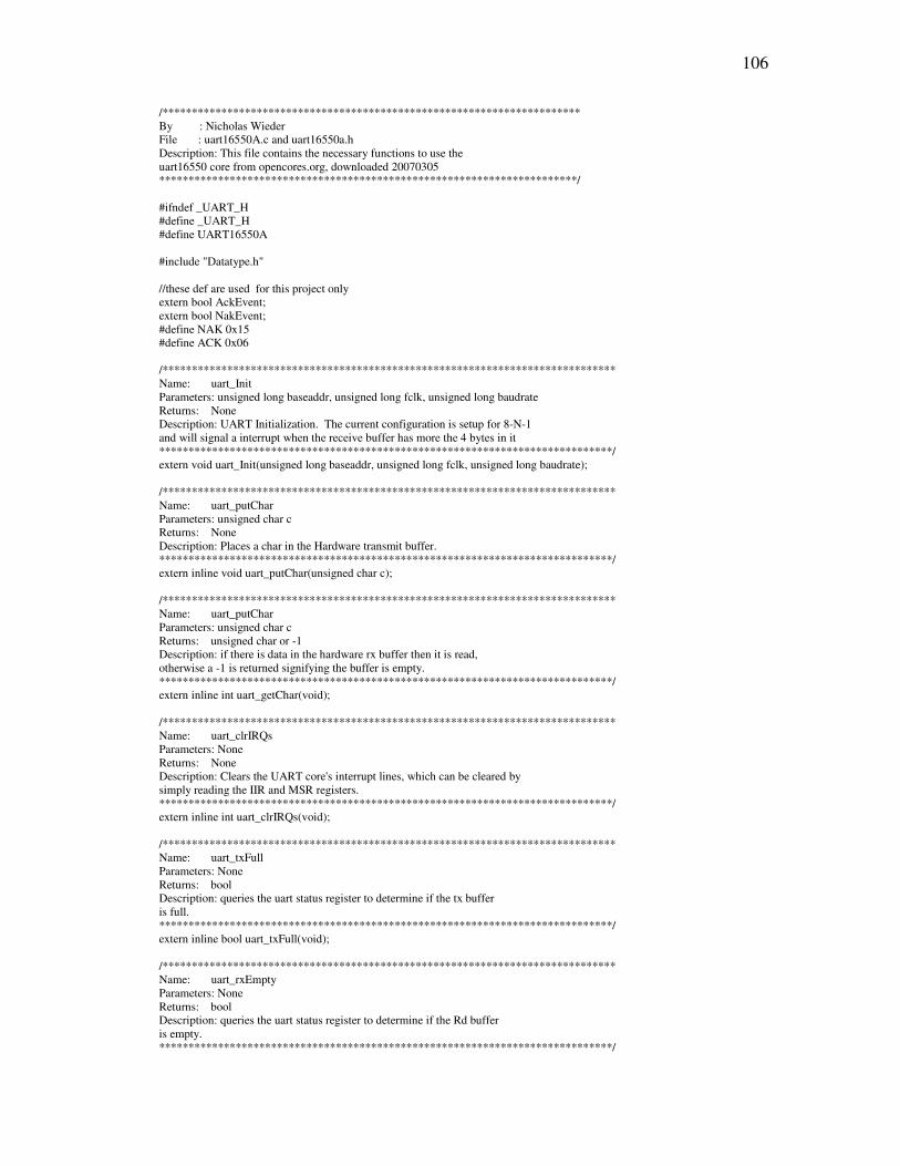
106
/*********************************************************************** By : Nicholas Wieder File : uart16550A.c and uart16550a.h Description: This file contains the necessary functions to use the uart16550 core from opencores.org, downloaded 20070305 ***********************************************************************/ #ifndef _UART_H #define _UART_H #define UART16550A #include "Datatype.h" //these def are used for this project only extern bool AckEvent; extern bool NakEvent; #define NAK 0x15 #define ACK 0x06 /***************************************************************************** Name: uart_Init Parameters: unsigned long baseaddr, unsigned long fclk, unsigned long baudrate Returns: None Description: UART Initialization. The current configuration is setup for 8-N-1 and will signal a interrupt when the receive buffer has more the 4 bytes in it *****************************************************************************/ extern void uart_Init(unsigned long baseaddr, unsigned long fclk, unsigned long baudrate); /***************************************************************************** Name: uart_putChar Parameters: unsigned char c Returns: None Description: Places a char in the Hardware transmit buffer. *****************************************************************************/ extern inline void uart_putChar(unsigned char c); /***************************************************************************** Name: uart_putChar Parameters: unsigned char c Returns: unsigned char or -1 Description: if there is data in the hardware rx buffer then it is read, otherwise a -1 is returned signifying the buffer is empty. *****************************************************************************/ extern inline int uart_getChar(void); /***************************************************************************** Name: uart_clrIRQs Parameters: None Returns: None Description: Clears the UART core's interrupt lines, which can be cleared by simply reading the IIR and MSR registers. *****************************************************************************/ extern inline int uart_clrIRQs(void); /***************************************************************************** Name: uart_txFull Parameters: None Returns: bool Description: queries the uart status register to determine if the tx buffer is full. *****************************************************************************/ extern inline bool uart_txFull(void); /***************************************************************************** Name: uart_rxEmpty Parameters: None Returns: bool Description: queries the uart status register to determine if the Rd buffer is empty. *****************************************************************************/

107
extern inline bool uart_rxEmpty(void); /***************************************************************************** Name: uart_getStatus Parameters: None Returns: Int Description: returns the value of the line status register *****************************************************************************/ extern inline int uart_getStatus(void); /***************************************************************************** Name: uart_write Parameters: unsigned char * data, int size Returns: bool Description: writes the elements of the input array to the serial port. The return value represents success of the sensor receiving the commands. This function is specialize for this project. *****************************************************************************/ extern bool uart_write(unsigned char* data, int size); /***************************************************************************** Name: uart_readAllRegs Parameters: None Returns: bool Description: This function is very handy in debugging problems with this core *****************************************************************************/ extern bool uart_readAllRegs(void); #endif /* _UART_H */

108
/*********************************************************************** By: Nicholas Wieder Source File(s): WindowReader.c and WindowReader.h Description: This file contains functions used to store Reading packet data into a single point, and into a window. ***********************************************************************/ #include "WindowReader.h" #define NUM_TO_BLANK 8 #define NUM_TO_AVE 7 #define VOLTAGE_CONV 1.00711e-4 //3.3/32767.0 /***************************************************************************** Name : WindowReader_FillWindow Parameters : int currentR, int* window, int windowSize Returns : bool Description: A return value of TRUE means all needed points were received and the window is full *****************************************************************************/ BOOL WindowReader_FillWindow(int currentR, int* window, int windowSize) { static int currentPointIndex = 0; int thisPoint; if(currentR < windowSize) { // if the point is ready use it if(WindowReader_RSaver(currentR,&thisPoint)) { //the point was made so add it to the array then increment the pointer window[currentPointIndex++] = thisPoint; //check if this was the last point if(currentPointIndex == windowSize) { currentPointIndex = 0; return 1; } } } else // the current point is larger then the window { window[currentPointIndex] = 0; } //this will happen a lot; return 0; } /***************************************************************************** Name : WindowReader_RSaver Parameters : int currentR, int* window, int windowSize Returns : bool Description: A return value of TRUE means all needed Reading Packets were received and a full point has been return in *dest. *****************************************************************************/ BOOL WindowReader_RSaver(int currentR, int* dest) { static int Count = 0; static int runningSum; // wait for the number to blank to come in if(++Count > NUM_TO_BLANK) { runningSum += currentR; //if this was the last R Packet in this data point find the ave and return true

109
if(Count >= (NUM_TO_BLANK+NUM_TO_AVE)) { *dest = (runningSum / NUM_TO_AVE); runningSum = 0; Count = 0; return 1; } } // not ready yet return 0 twice *dest = 0; return 0; }

110
/*********************************************************************** By : Nicholas Wieder File : WindowReader.c and WindowReader.h Description: This file contains functions used to store Reading packet data into a single point, and into a window. ***********************************************************************/ #if !defined(WindowReader_H_) #define WindowReader_H_ #include "ReadingPacket.h" /***************************************************************************** Name : WindowReader_FillWindow Parameters : int currentR, int* window, int windowSize Returns : bool Description: A return value of TRUE means all needed points were received and the window is full *****************************************************************************/ extern BOOL WindowReader_FillWindow(int currentR, int* window, int windowSize); /***************************************************************************** Name : WindowReader_RSaver Parameters : int currentR, int* window, int windowSize Returns : bool Description: A return value of TRUE means all needed Reading Packets were received and a full point has been return in *dest. *****************************************************************************/ extern BOOL WindowReader_RSaver(int currentR, int* dest); #endif //WindowReader_H_