System Basis Chip TLE9263QX - Infineon Technologies
164
Automotive Power Data Sheet Rev. 1.1, 2014-09-26 TLE9263QX Mid-Range System Basis Chip Family Body System IC with Integrated Voltage Regulators, Power Management Functions, HS-CAN Transceiver supporting CAN FD and Multiple LIN Transceiver. Featuring Multiple High-Side Switches and High-Voltage Wake Inputs. System Basis Chip
Transcript of System Basis Chip TLE9263QX - Infineon Technologies

Automot ive Power
Data SheetRev. 1.1, 2014-09-26
TLE9263QXMid-Range System Basis Chip Family
Body System IC with Integrated Voltage Regulators, Power Management Functions, HS-CAN Transceiver supporting CAN FD and Multiple LIN Transceiver. Featuring Multiple High-Side Switches and High-Voltage Wake Inputs.
System Basis Chip

Data Sheet 2 Rev. 1.1, 2014-09-26
TLE9263QX
1 Overview . . . . . . . . . . . . . . . . . . . . . . . . . . . . . . . . . . . . . . . . . . . . . . . . . . . . . . . . . . . . . . . . . . . . . . . 5
2 Block Diagram . . . . . . . . . . . . . . . . . . . . . . . . . . . . . . . . . . . . . . . . . . . . . . . . . . . . . . . . . . . . . . . . . . . 7
3 Pin Configuration . . . . . . . . . . . . . . . . . . . . . . . . . . . . . . . . . . . . . . . . . . . . . . . . . . . . . . . . . . . . . . . . 83.1 Pin Assignment . . . . . . . . . . . . . . . . . . . . . . . . . . . . . . . . . . . . . . . . . . . . . . . . . . . . . . . . . . . . . . . . . . . 83.2 Pin Definitions and Functions . . . . . . . . . . . . . . . . . . . . . . . . . . . . . . . . . . . . . . . . . . . . . . . . . . . . . . . . 93.3 Hints for Unused Pins . . . . . . . . . . . . . . . . . . . . . . . . . . . . . . . . . . . . . . . . . . . . . . . . . . . . . . . . . . . . . 113.4 Hints for Alternate Pin Functions . . . . . . . . . . . . . . . . . . . . . . . . . . . . . . . . . . . . . . . . . . . . . . . . . . . . 11
4 General Product Characteristics . . . . . . . . . . . . . . . . . . . . . . . . . . . . . . . . . . . . . . . . . . . . . . . . . . . 124.1 Absolute Maximum Ratings . . . . . . . . . . . . . . . . . . . . . . . . . . . . . . . . . . . . . . . . . . . . . . . . . . . . . . . . 124.2 Functional Range . . . . . . . . . . . . . . . . . . . . . . . . . . . . . . . . . . . . . . . . . . . . . . . . . . . . . . . . . . . . . . . . 144.3 Thermal Resistance . . . . . . . . . . . . . . . . . . . . . . . . . . . . . . . . . . . . . . . . . . . . . . . . . . . . . . . . . . . . . . 154.4 Current Consumption . . . . . . . . . . . . . . . . . . . . . . . . . . . . . . . . . . . . . . . . . . . . . . . . . . . . . . . . . . . . . 16
5 System Features . . . . . . . . . . . . . . . . . . . . . . . . . . . . . . . . . . . . . . . . . . . . . . . . . . . . . . . . . . . . . . . . 205.1 Block Description of State Machine . . . . . . . . . . . . . . . . . . . . . . . . . . . . . . . . . . . . . . . . . . . . . . . . . . 215.1.1 Device Configuration and SBC Init Mode . . . . . . . . . . . . . . . . . . . . . . . . . . . . . . . . . . . . . . . . . . . . 225.1.1.1 Device Configuration . . . . . . . . . . . . . . . . . . . . . . . . . . . . . . . . . . . . . . . . . . . . . . . . . . . . . . . . . . 225.1.1.2 SBC Init Mode . . . . . . . . . . . . . . . . . . . . . . . . . . . . . . . . . . . . . . . . . . . . . . . . . . . . . . . . . . . . . . . 245.1.2 SBC Normal Mode . . . . . . . . . . . . . . . . . . . . . . . . . . . . . . . . . . . . . . . . . . . . . . . . . . . . . . . . . . . . . . 255.1.3 SBC Stop Mode . . . . . . . . . . . . . . . . . . . . . . . . . . . . . . . . . . . . . . . . . . . . . . . . . . . . . . . . . . . . . . . . 265.1.4 SBC Sleep Mode . . . . . . . . . . . . . . . . . . . . . . . . . . . . . . . . . . . . . . . . . . . . . . . . . . . . . . . . . . . . . . . 275.1.5 SBC Restart Mode . . . . . . . . . . . . . . . . . . . . . . . . . . . . . . . . . . . . . . . . . . . . . . . . . . . . . . . . . . . . . . 285.1.6 SBC Fail-Safe Mode . . . . . . . . . . . . . . . . . . . . . . . . . . . . . . . . . . . . . . . . . . . . . . . . . . . . . . . . . . . . 295.1.7 SBC Development Mode . . . . . . . . . . . . . . . . . . . . . . . . . . . . . . . . . . . . . . . . . . . . . . . . . . . . . . . . . 305.2 Wake Features . . . . . . . . . . . . . . . . . . . . . . . . . . . . . . . . . . . . . . . . . . . . . . . . . . . . . . . . . . . . . . . . . . 315.2.1 Cyclic Sense . . . . . . . . . . . . . . . . . . . . . . . . . . . . . . . . . . . . . . . . . . . . . . . . . . . . . . . . . . . . . . . . . . 315.2.1.1 Configuration and Operation of Cyclic Sense . . . . . . . . . . . . . . . . . . . . . . . . . . . . . . . . . . . . . . . 325.2.1.2 Cyclic Sense in Low Power Mode . . . . . . . . . . . . . . . . . . . . . . . . . . . . . . . . . . . . . . . . . . . . . . . . 355.2.2 Cyclic Wake . . . . . . . . . . . . . . . . . . . . . . . . . . . . . . . . . . . . . . . . . . . . . . . . . . . . . . . . . . . . . . . . . . . 365.2.3 Internal Timer . . . . . . . . . . . . . . . . . . . . . . . . . . . . . . . . . . . . . . . . . . . . . . . . . . . . . . . . . . . . . . . . . . 375.3 Supervision Features . . . . . . . . . . . . . . . . . . . . . . . . . . . . . . . . . . . . . . . . . . . . . . . . . . . . . . . . . . . . . 37
6 Voltage Regulator 1 . . . . . . . . . . . . . . . . . . . . . . . . . . . . . . . . . . . . . . . . . . . . . . . . . . . . . . . . . . . . . 386.1 Block Description . . . . . . . . . . . . . . . . . . . . . . . . . . . . . . . . . . . . . . . . . . . . . . . . . . . . . . . . . . . . . . . . 386.2 Functional Description . . . . . . . . . . . . . . . . . . . . . . . . . . . . . . . . . . . . . . . . . . . . . . . . . . . . . . . . . . . . 396.3 Electrical Characteristics . . . . . . . . . . . . . . . . . . . . . . . . . . . . . . . . . . . . . . . . . . . . . . . . . . . . . . . . . . 40
7 Voltage Regulator 2 . . . . . . . . . . . . . . . . . . . . . . . . . . . . . . . . . . . . . . . . . . . . . . . . . . . . . . . . . . . . . 437.1 Block Description . . . . . . . . . . . . . . . . . . . . . . . . . . . . . . . . . . . . . . . . . . . . . . . . . . . . . . . . . . . . . . . . 437.2 Functional Description . . . . . . . . . . . . . . . . . . . . . . . . . . . . . . . . . . . . . . . . . . . . . . . . . . . . . . . . . . . . 447.2.1 Short to Battery Protection . . . . . . . . . . . . . . . . . . . . . . . . . . . . . . . . . . . . . . . . . . . . . . . . . . . . . . . . 447.3 Electrical Characteristics . . . . . . . . . . . . . . . . . . . . . . . . . . . . . . . . . . . . . . . . . . . . . . . . . . . . . . . . . . 45
8 External Voltage Regulator 3 . . . . . . . . . . . . . . . . . . . . . . . . . . . . . . . . . . . . . . . . . . . . . . . . . . . . . . 488.1 Block Description . . . . . . . . . . . . . . . . . . . . . . . . . . . . . . . . . . . . . . . . . . . . . . . . . . . . . . . . . . . . . . . . 488.2 Functional Description . . . . . . . . . . . . . . . . . . . . . . . . . . . . . . . . . . . . . . . . . . . . . . . . . . . . . . . . . . . . 498.2.1 External Voltage Regulator as Independent Voltage Regulator . . . . . . . . . . . . . . . . . . . . . . . . . . . 508.2.2 External Voltage Regulator in Load Sharing Mode . . . . . . . . . . . . . . . . . . . . . . . . . . . . . . . . . . . . . 518.3 External Components . . . . . . . . . . . . . . . . . . . . . . . . . . . . . . . . . . . . . . . . . . . . . . . . . . . . . . . . . . . . . 528.4 Calculation of RSHUNT . . . . . . . . . . . . . . . . . . . . . . . . . . . . . . . . . . . . . . . . . . . . . . . . . . . . . . . . . . . . . 53
Table of Contents

TLE9263QX
Table of Contents
Data Sheet 3 Rev. 1.1, 2014-09-26
8.5 Unused Pins . . . . . . . . . . . . . . . . . . . . . . . . . . . . . . . . . . . . . . . . . . . . . . . . . . . . . . . . . . . . . . . . . . . . 538.6 Electrical Characteristics . . . . . . . . . . . . . . . . . . . . . . . . . . . . . . . . . . . . . . . . . . . . . . . . . . . . . . . . . . 54
9 High-Side Switch . . . . . . . . . . . . . . . . . . . . . . . . . . . . . . . . . . . . . . . . . . . . . . . . . . . . . . . . . . . . . . . 599.1 Block Description . . . . . . . . . . . . . . . . . . . . . . . . . . . . . . . . . . . . . . . . . . . . . . . . . . . . . . . . . . . . . . . . 599.2 Functional Description . . . . . . . . . . . . . . . . . . . . . . . . . . . . . . . . . . . . . . . . . . . . . . . . . . . . . . . . . . . . 599.2.1 Over and Under Voltage Switch Off . . . . . . . . . . . . . . . . . . . . . . . . . . . . . . . . . . . . . . . . . . . . . . . . . 609.2.2 Over Current Detection and Switch Off . . . . . . . . . . . . . . . . . . . . . . . . . . . . . . . . . . . . . . . . . . . . . . 609.2.3 Open Load Detection . . . . . . . . . . . . . . . . . . . . . . . . . . . . . . . . . . . . . . . . . . . . . . . . . . . . . . . . . . . . 609.2.4 HSx Operation in Different SBC Modes . . . . . . . . . . . . . . . . . . . . . . . . . . . . . . . . . . . . . . . . . . . . . . 609.2.5 PWM and Timer Function . . . . . . . . . . . . . . . . . . . . . . . . . . . . . . . . . . . . . . . . . . . . . . . . . . . . . . . . 619.3 Electrical Characteristics . . . . . . . . . . . . . . . . . . . . . . . . . . . . . . . . . . . . . . . . . . . . . . . . . . . . . . . . . . 62
10 High Speed CAN Transceiver . . . . . . . . . . . . . . . . . . . . . . . . . . . . . . . . . . . . . . . . . . . . . . . . . . . . . 6310.1 Block Description . . . . . . . . . . . . . . . . . . . . . . . . . . . . . . . . . . . . . . . . . . . . . . . . . . . . . . . . . . . . . . . . 6310.2 Functional Description . . . . . . . . . . . . . . . . . . . . . . . . . . . . . . . . . . . . . . . . . . . . . . . . . . . . . . . . . . . . 6310.2.1 CAN OFF Mode . . . . . . . . . . . . . . . . . . . . . . . . . . . . . . . . . . . . . . . . . . . . . . . . . . . . . . . . . . . . . . . . 6510.2.2 CAN Normal Mode . . . . . . . . . . . . . . . . . . . . . . . . . . . . . . . . . . . . . . . . . . . . . . . . . . . . . . . . . . . . . . 6510.2.3 CAN Receive Only Mode . . . . . . . . . . . . . . . . . . . . . . . . . . . . . . . . . . . . . . . . . . . . . . . . . . . . . . . . . 6610.2.4 CAN Wake Capable Mode . . . . . . . . . . . . . . . . . . . . . . . . . . . . . . . . . . . . . . . . . . . . . . . . . . . . . . . . 6610.2.5 TXD Time-out Feature . . . . . . . . . . . . . . . . . . . . . . . . . . . . . . . . . . . . . . . . . . . . . . . . . . . . . . . . . . . 6810.2.6 Bus Dominant Clamping . . . . . . . . . . . . . . . . . . . . . . . . . . . . . . . . . . . . . . . . . . . . . . . . . . . . . . . . . 6810.2.7 Under Voltage Detection . . . . . . . . . . . . . . . . . . . . . . . . . . . . . . . . . . . . . . . . . . . . . . . . . . . . . . . . . 6810.3 Electrical Characteristics . . . . . . . . . . . . . . . . . . . . . . . . . . . . . . . . . . . . . . . . . . . . . . . . . . . . . . . . . . 69
11 LIN Transceiver . . . . . . . . . . . . . . . . . . . . . . . . . . . . . . . . . . . . . . . . . . . . . . . . . . . . . . . . . . . . . . . . . 7511.1 Block Description . . . . . . . . . . . . . . . . . . . . . . . . . . . . . . . . . . . . . . . . . . . . . . . . . . . . . . . . . . . . . . . . 7511.1.1 LIN Specifications . . . . . . . . . . . . . . . . . . . . . . . . . . . . . . . . . . . . . . . . . . . . . . . . . . . . . . . . . . . . . . 7511.2 Functional Description . . . . . . . . . . . . . . . . . . . . . . . . . . . . . . . . . . . . . . . . . . . . . . . . . . . . . . . . . . . . 7611.2.1 LIN OFF Mode . . . . . . . . . . . . . . . . . . . . . . . . . . . . . . . . . . . . . . . . . . . . . . . . . . . . . . . . . . . . . . . . . 7611.2.2 LIN Normal Mode . . . . . . . . . . . . . . . . . . . . . . . . . . . . . . . . . . . . . . . . . . . . . . . . . . . . . . . . . . . . . . . 7711.2.3 LIN Receive Only Mode . . . . . . . . . . . . . . . . . . . . . . . . . . . . . . . . . . . . . . . . . . . . . . . . . . . . . . . . . . 7711.2.4 LIN Wake Capable Mode . . . . . . . . . . . . . . . . . . . . . . . . . . . . . . . . . . . . . . . . . . . . . . . . . . . . . . . . . 7811.2.5 TXD Time-out Feature . . . . . . . . . . . . . . . . . . . . . . . . . . . . . . . . . . . . . . . . . . . . . . . . . . . . . . . . . . . 7911.2.6 Bus Dominant Clamping . . . . . . . . . . . . . . . . . . . . . . . . . . . . . . . . . . . . . . . . . . . . . . . . . . . . . . . . . 7911.2.7 Under-Voltage Detection . . . . . . . . . . . . . . . . . . . . . . . . . . . . . . . . . . . . . . . . . . . . . . . . . . . . . . . . . 7911.2.8 Slope Selection . . . . . . . . . . . . . . . . . . . . . . . . . . . . . . . . . . . . . . . . . . . . . . . . . . . . . . . . . . . . . . . . 8011.2.9 Flash Programming via LIN . . . . . . . . . . . . . . . . . . . . . . . . . . . . . . . . . . . . . . . . . . . . . . . . . . . . . . . 8011.3 Electrical Characteristics . . . . . . . . . . . . . . . . . . . . . . . . . . . . . . . . . . . . . . . . . . . . . . . . . . . . . . . . . . 81
12 Wake and Voltage Monitoring Inputs . . . . . . . . . . . . . . . . . . . . . . . . . . . . . . . . . . . . . . . . . . . . . . . 8612.1 Block Description . . . . . . . . . . . . . . . . . . . . . . . . . . . . . . . . . . . . . . . . . . . . . . . . . . . . . . . . . . . . . . . . 8612.2 Functional Description . . . . . . . . . . . . . . . . . . . . . . . . . . . . . . . . . . . . . . . . . . . . . . . . . . . . . . . . . . . . 8712.2.1 Wake Input Configuration . . . . . . . . . . . . . . . . . . . . . . . . . . . . . . . . . . . . . . . . . . . . . . . . . . . . . . . . 8812.2.2 Alternate Measurement Function with WK1 and WK2 . . . . . . . . . . . . . . . . . . . . . . . . . . . . . . . . . . . 8912.2.2.1 Block Description . . . . . . . . . . . . . . . . . . . . . . . . . . . . . . . . . . . . . . . . . . . . . . . . . . . . . . . . . . . . . 8912.2.2.2 Functional Description . . . . . . . . . . . . . . . . . . . . . . . . . . . . . . . . . . . . . . . . . . . . . . . . . . . . . . . . . 8912.3 Electrical Characteristics . . . . . . . . . . . . . . . . . . . . . . . . . . . . . . . . . . . . . . . . . . . . . . . . . . . . . . . . . . 90
13 Interrupt Function . . . . . . . . . . . . . . . . . . . . . . . . . . . . . . . . . . . . . . . . . . . . . . . . . . . . . . . . . . . . . . . 9213.1 Block and Functional Description . . . . . . . . . . . . . . . . . . . . . . . . . . . . . . . . . . . . . . . . . . . . . . . . . . . . 9213.2 Electrical Characteristics . . . . . . . . . . . . . . . . . . . . . . . . . . . . . . . . . . . . . . . . . . . . . . . . . . . . . . . . . . 94
14 Fail Outputs . . . . . . . . . . . . . . . . . . . . . . . . . . . . . . . . . . . . . . . . . . . . . . . . . . . . . . . . . . . . . . . . . . . . 9514.1 Block and Functional Description . . . . . . . . . . . . . . . . . . . . . . . . . . . . . . . . . . . . . . . . . . . . . . . . . . . . 95

TLE9263QX
Table of Contents
Data Sheet 4 Rev. 1.1, 2014-09-26
14.1.1 General Purpose I/O Functionality of FO2 and FO3 as Alternate Function . . . . . . . . . . . . . . . . . . 9614.2 Electrical Characteristics . . . . . . . . . . . . . . . . . . . . . . . . . . . . . . . . . . . . . . . . . . . . . . . . . . . . . . . . . . 97
15 Supervision Functions . . . . . . . . . . . . . . . . . . . . . . . . . . . . . . . . . . . . . . . . . . . . . . . . . . . . . . . . . . . 9915.1 Reset Function . . . . . . . . . . . . . . . . . . . . . . . . . . . . . . . . . . . . . . . . . . . . . . . . . . . . . . . . . . . . . . . . . . 9915.1.1 Reset Output Description . . . . . . . . . . . . . . . . . . . . . . . . . . . . . . . . . . . . . . . . . . . . . . . . . . . . . . . . . 9915.1.2 Soft Reset Description . . . . . . . . . . . . . . . . . . . . . . . . . . . . . . . . . . . . . . . . . . . . . . . . . . . . . . . . . . 10015.2 Watchdog Function . . . . . . . . . . . . . . . . . . . . . . . . . . . . . . . . . . . . . . . . . . . . . . . . . . . . . . . . . . . . . . 10115.2.1 Time-Out Watchdog . . . . . . . . . . . . . . . . . . . . . . . . . . . . . . . . . . . . . . . . . . . . . . . . . . . . . . . . . . . . 10215.2.2 Window Watchdog . . . . . . . . . . . . . . . . . . . . . . . . . . . . . . . . . . . . . . . . . . . . . . . . . . . . . . . . . . . . . 10315.2.3 Watchdog Setting Check Sum . . . . . . . . . . . . . . . . . . . . . . . . . . . . . . . . . . . . . . . . . . . . . . . . . . . 10315.2.4 Watchdog during SBC Stop Mode . . . . . . . . . . . . . . . . . . . . . . . . . . . . . . . . . . . . . . . . . . . . . . . . . 10415.2.5 Watchdog Start in SBC Stop Mode due to Bus Wake . . . . . . . . . . . . . . . . . . . . . . . . . . . . . . . . . . 10415.3 VS Power On Reset . . . . . . . . . . . . . . . . . . . . . . . . . . . . . . . . . . . . . . . . . . . . . . . . . . . . . . . . . . . . . 10515.4 Under Voltage VS and VSHS . . . . . . . . . . . . . . . . . . . . . . . . . . . . . . . . . . . . . . . . . . . . . . . . . . . . . . 10615.5 Over Voltage VSHS . . . . . . . . . . . . . . . . . . . . . . . . . . . . . . . . . . . . . . . . . . . . . . . . . . . . . . . . . . . . . 10615.6 VCC1 Over-/ Under Voltage and Under Voltage Prewarning . . . . . . . . . . . . . . . . . . . . . . . . . . . . . . 10615.6.1 VCC1 Under Voltage and Under Voltage Prewarning . . . . . . . . . . . . . . . . . . . . . . . . . . . . . . . . . . 10615.6.2 VCC1 Over Voltage . . . . . . . . . . . . . . . . . . . . . . . . . . . . . . . . . . . . . . . . . . . . . . . . . . . . . . . . . . . . 10715.7 VCC1 Short Circuit and VCC3 Diagnostics . . . . . . . . . . . . . . . . . . . . . . . . . . . . . . . . . . . . . . . . . . . 10815.8 VCC2 Undervoltage and VCAN Undervoltage . . . . . . . . . . . . . . . . . . . . . . . . . . . . . . . . . . . . . . . . . 10815.9 Thermal Protection . . . . . . . . . . . . . . . . . . . . . . . . . . . . . . . . . . . . . . . . . . . . . . . . . . . . . . . . . . . . . . 10915.9.1 Individual Thermal Shutdown . . . . . . . . . . . . . . . . . . . . . . . . . . . . . . . . . . . . . . . . . . . . . . . . . . . . 10915.9.2 Temperature Prewarning . . . . . . . . . . . . . . . . . . . . . . . . . . . . . . . . . . . . . . . . . . . . . . . . . . . . . . . . 11015.9.3 SBC Thermal Shutdown . . . . . . . . . . . . . . . . . . . . . . . . . . . . . . . . . . . . . . . . . . . . . . . . . . . . . . . . 11015.10 Electrical Characteristics . . . . . . . . . . . . . . . . . . . . . . . . . . . . . . . . . . . . . . . . . . . . . . . . . . . . . . . . . 111
16 Serial Peripheral Interface . . . . . . . . . . . . . . . . . . . . . . . . . . . . . . . . . . . . . . . . . . . . . . . . . . . . . . . 11416.1 SPI Block Description . . . . . . . . . . . . . . . . . . . . . . . . . . . . . . . . . . . . . . . . . . . . . . . . . . . . . . . . . . . . 11416.2 Failure Signalization in the SPI Data Output . . . . . . . . . . . . . . . . . . . . . . . . . . . . . . . . . . . . . . . . . . 11516.3 SPI Programming . . . . . . . . . . . . . . . . . . . . . . . . . . . . . . . . . . . . . . . . . . . . . . . . . . . . . . . . . . . . . . . 11716.4 SPI Bit Mapping . . . . . . . . . . . . . . . . . . . . . . . . . . . . . . . . . . . . . . . . . . . . . . . . . . . . . . . . . . . . . . . . 11916.5 SPI Control Registers . . . . . . . . . . . . . . . . . . . . . . . . . . . . . . . . . . . . . . . . . . . . . . . . . . . . . . . . . . . . 12216.5.1 General Control Registers . . . . . . . . . . . . . . . . . . . . . . . . . . . . . . . . . . . . . . . . . . . . . . . . . . . . . . . 12316.6 SPI Status Information Registers . . . . . . . . . . . . . . . . . . . . . . . . . . . . . . . . . . . . . . . . . . . . . . . . . . . 14016.6.1 General Status Registers . . . . . . . . . . . . . . . . . . . . . . . . . . . . . . . . . . . . . . . . . . . . . . . . . . . . . . . . 14116.6.2 Family and Product Information Register . . . . . . . . . . . . . . . . . . . . . . . . . . . . . . . . . . . . . . . . . . . 15216.7 Electrical Characteristics . . . . . . . . . . . . . . . . . . . . . . . . . . . . . . . . . . . . . . . . . . . . . . . . . . . . . . . . . 153
17 Application Information . . . . . . . . . . . . . . . . . . . . . . . . . . . . . . . . . . . . . . . . . . . . . . . . . . . . . . . . . 15517.1 Application Diagram . . . . . . . . . . . . . . . . . . . . . . . . . . . . . . . . . . . . . . . . . . . . . . . . . . . . . . . . . . . . . 15517.2 ESD Tests . . . . . . . . . . . . . . . . . . . . . . . . . . . . . . . . . . . . . . . . . . . . . . . . . . . . . . . . . . . . . . . . . . . . . 15917.3 Thermal Behavior of Package . . . . . . . . . . . . . . . . . . . . . . . . . . . . . . . . . . . . . . . . . . . . . . . . . . . . . 160
18 Package Outlines . . . . . . . . . . . . . . . . . . . . . . . . . . . . . . . . . . . . . . . . . . . . . . . . . . . . . . . . . . . . . . 162
19 Revision History . . . . . . . . . . . . . . . . . . . . . . . . . . . . . . . . . . . . . . . . . . . . . . . . . . . . . . . . . . . . . . . 163

PG-VQFN-48-31
Type Package MarkingTLE9263QX PG-VQFN-48-31 TLE9263QX
Data Sheet 5 Rev. 1.1, 2014-09-26
Mid-Range System Basis Chip Family
TLE9263QX
1 Overview
Scalable System Basis Chip Family• Product family with various products for complete scalable application
coverage. • Dedicated Data Sheets are available for the different product variants• Complete compatibility (hardware and software) across the family• TLE9263 with 2 LIN transceivers, 3 voltage regulators• TLE9262 with 1 LIN transceiver, 3 voltage regulators• TLE9261 without LIN transceivers, 3 voltage regulators• TLE9260 without LIN transceivers, 2 voltage regulators• Product variants for 5V (TLE926xQX) and 3.3V (TLE926xQXV33) output voltage for main voltage regulator• CAN Partial Networking variants for 5V (TLE926x-3QX) and 3.3V (TLE926x-3QXV33) output voltage
Device DescriptionThe TLE9263QX is a monolithic integrated circuit in an exposed pad VQFN-48 (7mm x 7mm) power package withLead Tip Inspection (LTI) feature to support Automatic Optical Inspection (AOI). The device is designed for various CAN-LIN automotive applications as main supply for the microcontroller andas interface for a LIN and CAN bus network.To support these applications, the System Basis Chip (SBC) provides the main functions, such as a 5V low-dropout voltage regulator (LDO) for e.g. a microcontroller supply, another 5V low-dropout voltage regulator withoff-board protection for e.g. sensor supply, another 5V/3.3V regulator to drive an external PNP transistor, whichcan be used as an independent supply for off-board usage or in load sharing configuration with the main regulatorVCC1, a HS-CAN transceiver supporting CAN FD and LIN transceiver for data transmission, high-side switcheswith embedded protective functions and a 16-bit Serial Peripheral Interface (SPI) to control and monitor the device.Also implemented are a configurable timeout / window watchdog circuit with a reset feature, three Fail Outputsand an under voltage reset feature. The device offers low-power modes in order to minimize current consumption on applications that are connectedpermanently to the battery. A wake-up from the low-power mode is possible via a message on the buses, via thebi-level sensitive monitoring/wake-up inputs as well as via cyclic wake.The device is designed to withstand the severe conditions of automotive applications.

TLE9263QX
Overview
Data Sheet 6 Rev. 1.1, 2014-09-26
Key Features• Very low quiescent current consumption in Stop- and Sleep Mode• Periodic Cyclic Wake in SBC Normal- and Stop Mode• Periodic Cyclic Sense in SBC Normal-, Stop- and Sleep Mode• Low-Drop Voltage Regulator 5V, 250mA• Low-Drop Voltage Regulator 5V, 100mA, protected features for off-board usage• Low-Drop Voltage Regulator, driving an external PNP transistor - 5V in load sharing configuration or 5V/3.3V
in stand-alone configuration, protected features for off-board usage. Current limitation by shunt resistor (up to 350mA with 470mΩ external shunt resistor) in stand-alone configuration
• High-Speed CAN Transceiver: – fully compliant to ISO11898-2 and ISO11898-5– suitable for chokeless operation up to 500kbps– supporting CAN FD communication up to 2 Mbps
• Two LIN Transceivers LIN 2.2, J2602 with configurable TXD timeout feature and LIN Flash Mode• Fully compliant to “Hardware Requirements for LIN, CAN and FlexRay Interfaces in Automotive Applications”
Revision 1.3, 2012-05-04• Four High-Side Outputs 7Ω typ. • Dedicated supply pin for High-Side Outputs• Two General Purpose High-Voltage In- and Outputs (GPIOs) configurable as add. Fail Outputs, Wake Inputs,
Low-Side switches or High-Side switches• Three universal High-Voltage Wake Inputs for voltage level monitoring • Alternate High-Voltage Measurement Function, e.g. for battery voltage sensing• Configurable wake-up sources• Reset Output• Configurable timeout and window watchdog• Up to three Fail Outputs (depending on configuration)• Over temperature and short circuit protection feature• Wide supply input voltage and temperature range• Software compatible to all SBC families TLE926x and TLE927x• Green Product (RoHS compliant) & AEC Qualified• PG-VQFN-48 leadless exposed-pad power package with Lead Tip Inspection (LTI) feature to support
Automatic Optical Inspection (AOI)

TLE9263QX
Block Diagram
Data Sheet 7 Rev. 1.1, 2014-09-26
2 Block Diagram
Figure 1 Block Diagram
VCC1
SPI
InterruptControl
SBCSTATE
MACHINE
SDISDO
CLKCSN
VCC
1
CAN cell
LIN cell
Window Watchdog
WK
TXDLIN 1RXDLIN 1
LIN 1
TXDCAN
RXDCAN
VCAN
CANH
CANL
WK1
RESETGENERATOR
INT
GND
WAKEREGISTER
VS
VS
Fail Safe
RO
FO3/TEST
LIN cellTXDLIN 2RXDLIN 2
LIN 2
FO2
FO1
VCC2 VCC2
High SideHS2
HS3HS4
HS1
WK WK2
WK WK3
VCC3
VCC
3REF
VC
C3SH
VCC
3B
VSHS VS
VSHS
Alternative function for FO2/3: GPIO1/2
Alternative function for WK 1/2: Voltage measurement

TLE9263QX
Pin Configuration
Data Sheet 8 Rev. 1.1, 2014-09-26
3 Pin Configuration
3.1 Pin Assignment
Figure 2 Pin Configuration
TLE9263
PG-VQFN-48
TLE9263.vsd
1G
ND
2 n.c.3 V
CC3RE
F4 V
CC3B
5 VCC
3SH
6 n.c.7 n.c.8
HS1
9 HS2
10 HS3
11 HS4
12 n.c.
FO3/TEST 48FO2 47n.c. 46n.c. 45
LIN2 44GND 43LIN1 42n.c. 41
CANH 40CANL 39GND 38
VCAN 37
13 VSHS14 VS15 VS16 n.c.17 VCC118 VCC219 n.c.20 GND21 FO122 WK123 WK224 WK3
25 T
XDLI
N226
RX
DLI
N2
27 C
LK28
SD
I29
SD
O30
CS
N31
INT
32 R
O33
TXD
LIN1
34 R
XD
LIN
135
TXD
CAN
36 R
XD
CAN

TLE9263QX
Pin Configuration
Data Sheet 9 Rev. 1.1, 2014-09-26
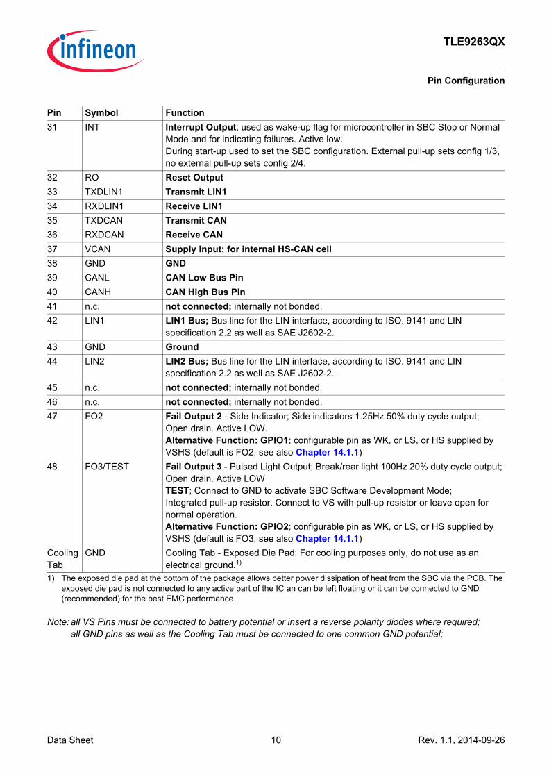
3.2 Pin Definitions and Functions
Pin Symbol Function1 GND Ground2 n.c. not connected; internally not bonded.3 VCC3REF VCC3REF; Collector connection for external PNP, reference input4 VCC3B VCC3B; Base connection for external PNP5 VCC3SH VCC3SH; Emitter connection for external PNP, shunt connection 6 n.c. not connected; internally not bonded.7 n.c. not connected; internally not bonded.8 HS1 High Side Output 1; typ. 7Ω9 HS2 High Side Output 2; typ. 7Ω10 HS3 High Side Output 3; typ. 7Ω11 HS4 High Side Output 4; typ. 7Ω12 n.c not connected; internally not bonded.13 VSHS Supply Voltage HS, LIN and GPIO1/2 in HS configuration; Supply voltage for
High-Side Switches and LIN modules and respective UV-/OV supervision; Connected to battery voltage with reverse protection diode and filter against EMC; connect to VS if separate supply is not needed
14 VS Supply Voltage; Supply voltage for chip internal supply and voltage regulators; Connected to Battery Voltage with external reverse protection Diode and Filter against EMC
15 VS Supply Voltage; Supply voltage for chip internal supply and voltage regulators; Connected to Battery Voltage with external reverse protection Diode and Filter against EMC
16 n.c. not connected; internally not bonded.17 VCC1 Voltage Regulator Output 118 VCC2 Voltage Regulator Output 219 n.c. not connected; internally not bonded.20 GND GND21 FO1 Fail Output 122 WK1 Wake Input 1; Alternative function: HV-measurement function input pin
(only in combination with WK2, see Chapter 12.2.2)23 WK2 Wake Input 2; Alternative function: HV-measurement function output pin
(only in combination with WK1, see Chapter 12.2.2)24 WK3 Wake Input 325 TXDLIN2 Transmit LIN226 RXDLIN2 Receive LIN2 27 CLK SPI Clock Input28 SDI SPI Data Input; into SBC (=MOSI)29 SDO SPI Data Output; out of SBC (=MISO)30 CSN SPI Chip Select Not Input
TLE9263QX
Pin Configuration
Data Sheet 10 Rev. 1.1, 2014-09-26
Note: all VS Pins must be connected to battery potential or insert a reverse polarity diodes where required; all GND pins as well as the Cooling Tab must be connected to one common GND potential;
31 INT Interrupt Output; used as wake-up flag for microcontroller in SBC Stop or Normal Mode and for indicating failures. Active low. During start-up used to set the SBC configuration. External pull-up sets config 1/3, no external pull-up sets config 2/4.
32 RO Reset Output33 TXDLIN1 Transmit LIN134 RXDLIN1 Receive LIN135 TXDCAN Transmit CAN36 RXDCAN Receive CAN37 VCAN Supply Input; for internal HS-CAN cell38 GND GND 39 CANL CAN Low Bus Pin40 CANH CAN High Bus Pin41 n.c. not connected; internally not bonded.42 LIN1 LIN1 Bus; Bus line for the LIN interface, according to ISO. 9141 and LIN
specification 2.2 as well as SAE J2602-2.43 GND Ground44 LIN2 LIN2 Bus; Bus line for the LIN interface, according to ISO. 9141 and LIN
specification 2.2 as well as SAE J2602-2.45 n.c. not connected; internally not bonded.46 n.c. not connected; internally not bonded.47 FO2 Fail Output 2 - Side Indicator; Side indicators 1.25Hz 50% duty cycle output;
Open drain. Active LOW. Alternative Function: GPIO1; configurable pin as WK, or LS, or HS supplied by VSHS (default is FO2, see also Chapter 14.1.1)
48 FO3/TEST Fail Output 3 - Pulsed Light Output; Break/rear light 100Hz 20% duty cycle output;Open drain. Active LOWTEST; Connect to GND to activate SBC Software Development Mode; Integrated pull-up resistor. Connect to VS with pull-up resistor or leave open for normal operation. Alternative Function: GPIO2; configurable pin as WK, or LS, or HS supplied by VSHS (default is FO3, see also Chapter 14.1.1)
Cooling Tab
GND Cooling Tab - Exposed Die Pad; For cooling purposes only, do not use as an electrical ground.1)
1) The exposed die pad at the bottom of the package allows better power dissipation of heat from the SBC via the PCB. The exposed die pad is not connected to any active part of the IC an can be left floating or it can be connected to GND (recommended) for the best EMC performance.
Pin Symbol Function
TLE9263QX
Pin Configuration
Data Sheet 11 Rev. 1.1, 2014-09-26
3.3 Hints for Unused PinsIt must be ensured that the correct configurations are also selected, i.e. in case functions are not used that theyare disabled via SPI:• WK1/2/3: connect to GND and disable WK inputs via SPI• HSx: leave open• LINx, RXDLINx, TXDLINx, CANH/L, RXDCAN, TXDCAN: leave all pins open• RO / FOx: leave open• INT: leave open• TEST: connect to GND during power-up to activate SBC Development Mode;
connect to VS or leave open for normal user mode operation• VCC2: leave open and keep disabled• VCC3: See Chapter 8.5• VCAN: connect to VCC1• n.c.: not connected; internally not bonded; connect to GND• If unused pins are routed to an external connector which leaves the ECU, then these pins should have
provision for a zero ohm jumper (depopulated if unused) or ESD protection.
3.4 Hints for Alternate Pin FunctionsIn case of alternate pin functions, selectable via SPI, it must be ensured that the correct configurations are alsoselected via SPI, in case it is not done automatically. Please consult the respective chapter. In addition, followingtopics shall be considered:• WK1..2: The pins can be either used as HV wake / voltage monitoring inputs or for a voltage measurement
function (via bit WK_MEAS). In the second case, the WK1..2 pins shall not be used / assigned for any wake detection nor cyclic sense functionality, i.e. WK1 and WK2 must be disabled in the register WK_CTRL_2 and the level information is to be ignored in the register WK_LVL_STAT.
• FO2..3: The pins can also be configured as GPIOs in the GPIO_CTRL register. In this case, the pins shall not be used for any fail output functionality. The default function after Power on Reset (POR) is FOx.

TLE9263QX
General Product Characteristics
Data Sheet 12 Rev. 1.1, 2014-09-26
4 General Product Characteristics
4.1 Absolute Maximum Ratings
Table 1 Absolute Maximum Ratings1)
Tj = -40 °C to +150 °C; all voltages with respect to ground, positive current flowing into pin(unless otherwise specified)Parameter Symbol Values Unit Note /
Test ConditionNumber
Min. Typ. Max.VoltagesSupply Voltage (VS, VSHS) VSx, max -0.3 – 28 V – P_4.1.1Supply Voltage (VS, VSHS) VSx, max -0.3 – 40 V Load Dump,
max. 400 msP_4.1.2
Voltage Regulator 1 VCC1, max -0.3 – 5.5 V – P_4.1.3Voltage Regulator 2 VCC2, max -0.3 – 28 V VCC2 = 40V for
Load Dump, max. 400 ms;
P_4.1.4
Voltage Regulator 3 (VCC3REF)
VCC3REF,max -0.3 – 28 V VCC3REF = 40V for Load Dump, max. 400 ms;
P_4.1.5
Voltage Regulator 3 (VCC3B) VCC3B,max -0.3 – VS + 10
V VCC3B = 40V for Load Dump, max. 400 ms;
P_4.1.25
Voltage Regulator 3 (VCC3SH)
VCC3SH,max VS- 0.30
– VS + 0.30
V – P_4.1.26
Wake Inputs WK1..3 VWK, max -0.3 – 40 V – P_4.1.6Fail Pin FO1 VFO1, max -0.3 – 40 V – P_4.1.7Fail Pins FO2, FO3/TEST VFO2_3, max -0.3 – VS
+ 0.3V – P_4.1.23
LINx, CANH, CANL VBUS, max -27 – 40 V – P_4.1.8Logic Input Pins (CSN, CLK, SDI, TXDLINx, TXDCAN)
VI, max -0.3 – VCC1+ 0.3
V – P_4.1.9
Logic Output Pins (SDO, RO, INT, RXDLINx, RXDCAN)
VO, max -0.3 – VCC1+ 0.3
V – P_4.1.10
VCAN Input Voltage VVCAN, max -0.3 – 5.5 V – P_4.1.11High Side 1...4 VHS, max -0.3 – VSHS
+ 0.3V – P_4.1.12
CurrentsWake input WK1 IWK1,max 0 – 500 µA 2) P_4.1.13Wake input WK2 IWK2,max -500 – 0 µA 2) P_4.1.14TemperaturesJunction Temperature Tj -40 – 150 °C – P_4.1.15Storage Temperature Tstg -55 – 150 °C – P_4.1.16

TLE9263QX
General Product Characteristics
Data Sheet 13 Rev. 1.1, 2014-09-26
Notes1. Stresses above the ones listed here may cause permanent damage to the device. Exposure to absolute
maximum rating conditions for extended periods may affect device reliability.2. Integrated protection functions are designed to prevent IC destruction under fault conditions described in the
data sheet. Fault conditions are considered as “outside” normal operating range. Protection functions are not designed for continuous repetitive operation.
ESD SusceptibilityESD Resistivity VESD,11 -2 – 2 kV HBM3) P_4.1.17ESD Resistivity to GND, HSx VESD,12 -2 – 2 kV HBM3) P_4.1.18ESD Resistivity to GND, CANH, CANL, LINx
VESD,13 -8 – 8 kV HBM4)3) P_4.1.19
ESD Resistivity to GND VESD,21 -500 – 500 V CDM5) P_4.1.20ESD Resistivity Pin 1, 12,13,24,25,36,37,48 (corner pins) to GND
VESD,22 -750 – 750 V CDM5) P_4.1.21
1) Not subject to production test, specified by design.2) Applies only if WK1 and WK2 are configured as alternative HV-measurement function3) ESD susceptibility, HBM according to ANSI/ESDA/JEDEC JS-001 (1.5 kΩ, 100 pF)4) For ESD “GUN” Resistivity 6KV (according to IEC61000-4-2 “gun test” (150pF, 330Ω)), will be shown in Application
Information and test report will be provided from IBEE5) ESD susceptibility, Charged Device Model “CDM” EIA/JESD22-C101 or ESDA STM5.3.1
Table 1 Absolute Maximum Ratings1) (cont’d)Tj = -40 °C to +150 °C; all voltages with respect to ground, positive current flowing into pin(unless otherwise specified)Parameter Symbol Values Unit Note /
Test ConditionNumber
Min. Typ. Max.

TLE9263QX
General Product Characteristics
Data Sheet 14 Rev. 1.1, 2014-09-26
4.2 Functional Range
Note: Within the functional range the IC operates as described in the circuit description. The electrical characteristics are specified within the conditions given in the related electrical characteristics table.
Device Behavior Outside of Specified Functional Range:• 28V < VS,func < 40V: Device will still be functional including the state machine; the specified electrical
characteristics might not be ensured anymore. The regulators VCC1/2/3 are working properly, however, a thermal shutdown might occur due to high power dissipation. HSx switches might be turned OFF depending on VSHS_OV configurations. The specified SPI communication speed is ensured; the absolute maximum ratings are not violated, however the device is not intended for continuous operation of VS >28V. The device operation at high junction temperatures for long periods might reduce the operating life time;
• 18V < VS,LIN <28V: The LIN transceiver is still functional. However, the communication might fail due to out-of-LIN-spec operation;
• VSHS,UVD < VS,LIN < 6V: The LIN transceiver is still functional. However, the communication might fail due to out-of-LIN-spec operation;
• VCAN < 4.75V: The undervoltage bit VCAN_UV will be set in the SPI register BUS_STAT_1 and the transmitter will be disabled as long as the UV condition is present;
• 5.25V < VCAN < 5.50V: CAN transceiver still functional. However, the communication might fail due to out-of-spec operation;
• VPOR,f < VS < 5.5V: Device will still be functional; the specified electrical characteristics might not be ensured anymore. – The voltage regulators will enter the low-drop operation mode
(applies for VCC3 only if bit VCC3_VS_ UV_OFF is set),– A VCC1_UV reset could be triggered depending on the Vrtx settings,– The LIN transmitter will be disabled if VSHS,UVD is reached, – HSx switch behavior will depend on the respective configuration:
- HS_UV_SD_EN = ‘0’ (default): HSx will be turned OFF for VSHS < VSHS_UV and will stay OFF;- HS_UV_SD_EN = ‘1’: HSx stays on as long as possible. An unwanted over current shut down may occur. OC shut down bit set and the respective HSx switch will stay OFF;
– FOx outputs will remain ON if they were enabled before VS > 5.5V,– The specified SPI communication speed is ensured.
Table 2 Functional RangeParameter Symbol Values Unit Note /
Test ConditionNumber
Min. Typ. Max.Supply Voltage VS,func VPOR – 28 V 1) VPOR see
section Chapter 15.10
1) Including Power-On Reset, Over- and Under voltage Protection
P_4.2.1
LIN Bus Voltage VS,LIN,func 6 – 18 V 2)
2) Parameter Specification according to LIN 2.2 standard
P_4.2.2CAN Supply Voltage VCAN,func 4.75 – 5.25 V – P_4.2.3SPI frequency fSPI – – 4 MHz see Chapter 16.7
for fSPI,max
P_4.2.4
Junction Temperature Tj -40 – 150 °C – P_4.2.5

TLE9263QX
General Product Characteristics
Data Sheet 15 Rev. 1.1, 2014-09-26
4.3 Thermal Resistance
Table 3 Thermal Resistance1)
1) Not subject to production test, specified by design.
Parameter Symbol Values Unit Note / Test Condition
NumberMin. Typ. Max.
Junction to Soldering Point RthJSP – 6 – K/W Exposed Pad P_4.3.1Junction to Ambient RthJA – 33 – K/W 2)
2) According to Jedec JESD51-2,-5,-7 at natural convection on FR4 2s2p board for 1.5W. Board: 76.2x114.3x1.5mm³ with 2 inner copper layers (35µm thick), with thermal via array under the exposed pad contacting the first inner copper layer and 300mm2 cooling area on the bottom layer (70µm).
P_4.3.2

TLE9263QX
General Product Characteristics
Data Sheet 16 Rev. 1.1, 2014-09-26
4.4 Current Consumption
Table 4 Current ConsumptionCurrent consumption values are specified at Tj = 25°C, VS = 13.5V, all outputs open (unless otherwise specified)Parameter Symbol Values Unit Note / Test Condition Number
Min. Typ. Max.SBC Normal ModeNormal Mode current consumption
INormal – 3.5 6.5 mA VS = 5.5 V to 28 V;Tj = -40 °C to +150 °C; VCC2, CAN, LIN, VCC3, HSx = OFF
P_4.4.1
SBC Stop ModeStop Mode current consumption
IStop_1,25 – 44 60 µA 1)VCC2/3, HSx = OFF; CAN, LINx, WKx not wake capable;Watchdog = OFF; no load on VCC1;I_PEAK_TH = ‘0’
P_4.4.2
Stop Mode current consumption
IStop_1,85 – 50 70 µA 1)2)Tj = 85°C; VCC2/3, HSx = OFF; CAN, LINx, WKx not wake capable;Watchdog = OFF; no load on VCC1;I_PEAK_TH = ‘0’
P_4.4.3
Stop Mode current consumption(high active peak threshold)
IStop_2,25 – 64 90 µA 1)VCC2/3, HSx = OFF; CAN, LINx, WKx not wake capable;Watchdog = OFF; no load on VCC1;I_PEAK_TH = ‘1’
P_4.4.35
Stop Mode current consumption(high active peak threshold)
IStop_2,85 – 70 100 µA 1)2)Tj = 85°C; VCC2/3, HSx = OFF; CAN, LINx, WKx not wake capable;Watchdog = OFF; no load on VCC1;I_PEAK_TH = ‘1’
P_4.4.36
SBC Sleep ModeSleep Mode current consumption
ISleep,25 – 15 25 µA VCC2/3, HSx = OFF; CAN, LINx, WKx not wake capable
P_4.4.5
Sleep Mode current consumption
ISleep,85 – 25 35 µA 2)Tj = 85°C; VCC2/3, HSx = OFF; CAN, LINx, WKx not wake capable
P_4.4.6

TLE9263QX
General Product Characteristics
Data Sheet 17 Rev. 1.1, 2014-09-26
Feature Incremental Current ConsumptionCurrent consumption for CAN module, recessive state
ICAN,rec – 2 3 mA SBC Normal/Stop Mode; CAN Normal Mode; VCC1 connected to VCAN; VTXDCAN = VCC1; no RL on CAN
P_4.4.7
Current consumption for CAN module, dominant state
ICAN,dom – 3 4.5 mA 2)SBC Normal/Stop Mode; CAN Normal Mode; VCC1 connected to VCAN; VTXDCAN = GND; no RL on CAN
P_4.4.8
Current consumption for CAN module, Receive Only Mode
ICAN,RcvOnly – 0.9 1.2 mA 2)SBC Normal/Stop Mode; CAN Receive Only Mode; VCC1 connected to VCAN; VTXDCAN = VCC1; no RL on CAN
P_4.4.9
Current consumption per LIN module, recessive state
ILIN,rec – 0.1 1 mA SBC Normal/Stop Mode; LIN Normal Mode; VTXDLIN = VCC1; no RL on LIN
P_4.4.10
Current consumption per LIN module, dominant state
ILIN,dom – 1.0 1.5 mA 2)SBC Normal/Stop Mode; LIN Normal Mode; VTXDLIN = GND; no RL on LIN
P_4.4.11
Current consumption per LIN module, Receive Only Mode
ILIN,RcvOnly – 0.2 0.5 mA 2)SBC Normal/Stop Mode; LIN Receive Only Mode; VTXDLIN = VCC1; no RL on LIN
P_4.4.12
Current consumption for WK1..3 wake capability (all wake inputs)
IWake,WKx,25 – 0.2 2 µA 3)4)5) SBC Sleep Mode; WK1..3 wake capable (all WKx enabled); LIN, CAN = OFF
P_4.4.13
Current consumption for WK1..3 wake capability(all wake inputs)
IWake,WKx,85 – 0.5 3 µA 2)3)4)5)SBC Sleep Mode; Tj = 85°C; WK1..3 wake capable;(all WKx enabled); LIN, CAN = OFF
P_4.4.14
Table 4 Current Consumption (cont’d)Current consumption values are specified at Tj = 25°C, VS = 13.5V, all outputs open (unless otherwise specified)Parameter Symbol Values Unit Note / Test Condition Number
Min. Typ. Max.

TLE9263QX
General Product Characteristics
Data Sheet 18 Rev. 1.1, 2014-09-26
Current consumption per LIN module wake capability
IWake,LIN,25 – 0.2 2 µA 3)SBC Sleep Mode; LIN wake capable; WK1..3, CAN = OFF
P_4.4.15
Current consumption per LIN module wake capability
IWake,LIN,85 – 0.5 3 µA 2)3)SBC Sleep Mode; Tj = 85°C; LIN wake capable; WK1..3, CAN = OFF
P_4.4.16
Current consumption for CAN wake capability
IWake,CAN,25 – 4.5 6 µA 3)SBC Sleep Mode; CAN wake capable; WK1..3, LIN = OFF
P_4.4.17
Current consumption for CAN wake capability
IWake,CAN,85 – 5.5 7 µA 2)3)SBC Sleep Mode; Tj = 85°C; CAN wake capable; WK1..3, LIN = OFF
P_4.4.18
VCC2 Normal Mode current consumption
INormal,VCC2 – 2.5 3.5 mA VS = 5.5 V to 28 V;Tj = -40 °C to +150 °C; VCC2 = ON (no load)
P_4.4.32
Current consumption for VCC2 in SBC Sleep Mode
ISleep,VCC2,25 – 25 35 µA 1)3)SBC Sleep Mode; VCC2 = ON (no load);LIN, CAN, WK1..3 = OFF
P_4.4.19
Current consumption for VCC2 in SBC Sleep Mode
ISleep,VCC2,85 – 30 40 µA 1)2)3)SBC Sleep Mode; Tj = 85°C; VCC2 = ON (no load); LIN, CAN, WK1..3 = OFF
P_4.4.20
Current consumption for VCC3 in SBC Sleep Mode in stand-alone configuration
ISleep,VCC3,25 – 40 60 µA 1)3)SBC Sleep Mode; VCC3 = ON (no load, stand-along config.);LIN, CAN, WK1..3 = OFF
P_4.4.21
Current consumption for VCC3 in SBC Sleep Mode in stand-alone configuration
ISleep,VCC3,85 – 50 70 µA 1)2)3)SBC Sleep Mode; Tj = 85°C; VCC3 = ON (no load, stand-along config.); LIN, CAN, WK1..3 = OFF
P_4.4.22
Current consumption for HSx in SBC Stop Mode
IStop,HSx,25 – 525 650 µA 3)6)SBC Stop Mode; Cyclic Sense & HSx= ON (no load);LIN, CAN, WK1..3 = OFF
P_4.4.33
Table 4 Current Consumption (cont’d)Current consumption values are specified at Tj = 25°C, VS = 13.5V, all outputs open (unless otherwise specified)Parameter Symbol Values Unit Note / Test Condition Number
Min. Typ. Max.

TLE9263QX
General Product Characteristics
Data Sheet 19 Rev. 1.1, 2014-09-26
Note: There is no additional current consumption contribution due to PWM generators.
Current consumption for HSx in SBC Stop Mode
IStop,HSx,85 – 575 700 µA 2)3)6)SBC Stop Mode; Tj = 85°C; Cyclic Sense & HSx = ON (no load); LIN, CAN, WK1..3 = OFF
P_4.4.34
Current consumption for cyclic sense function
IStop,CS25 – 20 26 µA 3)7)8)SBC Stop Mode; WD = OFF
P_4.4.23
Current consumption for cyclic sense function
IStop,CS85 – 24 35 µA 2)3)7)8)SBC Stop Mode; Tj = 85°C; WD = OFF
P_4.4.27
Current consumption for watchdog active in Stop Mode
IStop,WD25 – 20 26 µA 2)SBC Stop Mode; Watchdog running
P_4.4.30
Current consumption for watchdog active in Stop Mode
IStop,WD85 – 24 35 µA 2)SBC Stop Mode; Tj = 85°C; Watchdog running
P_4.4.31
Current consumption for active fail outputs (FO1..3)
IStop,FOx – 1.0 2.0 mA 2)all SBC Modes;Tj = 25°C; FOx = ON (no load);
P_4.4.24
1) If the load current on VCC1 will exceed the configured VCC1 active peak threshold IVCC1,Ipeak1,r or IVCC1,Ipeak2,r, the current consumption will increase by typ. 2.9mA to ensure optimum dynamic load behavior. Same applies to VCC2. For VCC3 the current consumption will increase by typ. 1.4mA. See also Chapter 6, Chapter 7, Chapter 8.
2) Not subject to production test, specified by design.3) Current consumption adders of features defined for SBC Sleep Mode also apply for SBC Stop Mode and vice versa (unless
otherwise specified).4) No pull-up or pull-down configuration selected.5) The specified WKx current consumption adder for wake capability applies regardless how many WK inputs are activated.6) A typ. 75µA / max 125µA (Tj = 85°C) adder applies for every additionally activated HSx switch in SBC Stop Mode;
In SBC Normal Mode every HSx switch consumes the typ. 75µA / max 125µA (Tj = 85°C) without the initial adder because the biasing is already enabled.
7) HS1 used for cyclic sense, Timer 2, 20ms period, 0.1ms on-time, no load on HS1.
In general the current consumption adder for cyclic sense in SBC Stop Mode can be calculated with below equation:IStop,CS = 18µA + (525µA *tON/TPer)
8) Also applies to Cyclic Wake
Table 4 Current Consumption (cont’d)Current consumption values are specified at Tj = 25°C, VS = 13.5V, all outputs open (unless otherwise specified)Parameter Symbol Values Unit Note / Test Condition Number
Min. Typ. Max.

TLE9263QX
System Features
Data Sheet 20 Rev. 1.1, 2014-09-26
5 System Features
This chapter describes the system features and behavior of the TLE9263QX:• State machine• SBC mode control• Device configuration• State of supply and peripherals• System functions such as cyclic sense or cyclic wake• Supervision and diagnosis functions
The System Basis Chip (SBC) offers six operating modes: • SBC Init Mode: Power-up of the device and after a soft reset,• SBC Normal Mode: The main operating mode of the device, • SBC Stop Mode: The first-level power saving mode with the main voltage regulator VCC1 enabled,• SBC Sleep Mode: The second-level power saving mode with VCC1 disabled, • SBC Restart Mode: An intermediate mode after a wake event from SBC Sleep or Fail-Safe Mode or after a
failure (e.g. WD failure, VCC1 under voltage reset) to bring the microcontroller into a defined state via a reset. Once the failure condition is not present anymore the device will automatically change to SBC Normal Mode after a delay time (tRD1).
• SBC Fail-Safe Mode: A safe-state mode after critical failures (e.g. WD failure, VCC1 under voltage reset) to bring the system into a safe state and to ensure a proper restart of the system. VCC1 is disabled. It is a permanent state until either a wake event (via CAN, LINx or WKx) occurs or the over temperature condition is not present anymore.
A special mode, called SBC Development Mode, is available during software development or debugging of thesystem. All above mentioned operating modes can be accessed in this mode. However, the watchdog counter isstopped and does not need to be triggered. This mode can be accessed by setting the TEST pin to GND duringSBC Init Mode.
The device can be configured via hardware (external component) to determine the device behavior after awatchdog trigger failure. See Chapter 5.1.1 for further information.
The System Basis Chip is controlled via a 16-bit SPI interface. A detailed description can be found inChapter 16.The configuration as well as the diagnosis is handled via the SPI. The SPI mapping of the TLE9263QXis compatible to other devices of the TLE926x and TLE927x families.

TLE9263QX
System Features
Data Sheet 21 Rev. 1.1, 2014-09-26
5.1 Block Description of State Machine
The different SBC Modes are selected via SPI by setting the respective SBC MODE bits in the registerM_S_CTRL. The SBC MODE bits are cleared when going through SBC Restart Mode and thus always show thecurrent SBC mode.
Figure 3 State Diagram showing the SBC Operating Modes
SBC Init Mode *(Long open window)
VCC1ON
VCC2OFF
VCC3OFF
FOxinact.
CAN(3)
OFFLINx(3)
OFF
Wake up event
SPI cmd SPI cmd SPI cmd
Any SPI command
WD trigger
First battery connection
VCC1 Undervoltage
Automatic
1st Watchdog Failure Config 2,2nd Watchdog Failure, Config 4
VCC1 Short to GND
SBC Soft Reset
Reset is releasedWD starts with long open window
(1) After Fail-Safe Mode entry, the device will stay for at least typ . 1s in this mode (with RO low) after a TSD2 event and min. typ. 100ms after other Fail-Safe Events. Only then the device can leave the mode via a wake-up event. Wake events are stored during this time. (2) according to VCC3 configuration(3) For SBC Development Mode CAN/LINx/VCC2 are ON in SBC Init Mode and stay ON when going from there to SBC Normal Mode (4) See chapter CAN & LIN for detailed behavior in SBC Restart Mode(5) See Chapter 5.1.5 and 14.1 for detailed FOx behavior
WDConfig.
HSxOFF
SBC Normal Mode
VCC1ON
VCC2config.
VCC3config.
FOxact/inact
CAN(3)
config.LINx(3)
config.
WDconfig.
HSxconfig.
SBC Sleep Mode
VCC1OFF
VCC2fixed
FOxfixed
CANWake
capable /off
LINxWake
capable /off
WDOFF.
HSxfixed
SBC Stop Mode
VCC1ON
VCC2fixed
VCC3fixed
FOxfixed
CANfixed
LINxfixed
WDfixed
HSxfixed
SBC Restart Mode (RO pin is asserted)
VCC1ON/
ramping
VCC2OFF
FOx(5)
active/fixed
CAN (4)
woken / OFF
WDOFF
HSxOFF
SBC Fail-Safe Mode (1)
VCC1OFF
VCC2OFF
VCC3OFF
FOx(5)
activeCANWake
capable
WDOFF
HSxOFF
Config.: settings can be changed in this SBC mode ;
Fixed: settings stay as defined in SBC Normal Mode
TSD2 event,
LINxWake
capable
LINx (4)
woken / OFF
VCC3(2)
fixed/ramping
VCC3(2)
Fixed /OFF
* The SBC Development Modeis a super set of state machine where the WD timer is stopped and CAN/LINx behavior differs in SBC Init Mode . Otherwise,
there are no differences in behavior.
Cyc. WakeOFF
Cyc. SenseOFF
Cyc. Wakeconfig.
Cyc. Senseconfig.
Cyc. Wakefixed
Cyc. Sensefixed
Cyc. WakeOFF
Cyc. Sensefixed
Cyc. WakeOFF
Cyc. SenseOFF
Cyc. WakeOFF
Cyc. SenseOFF
CAN, LINx, WKx wake-up eventOR
Release of over temperature TSD2 after tTSD2
VCC1 over voltage Config 2/4 (if VCC_OV_RST set)
VCC1 over voltage Config 1/3 (if VCC_OV_RST set)
Watchdog Failure: Config 1/3 & 1st WD failure
in Config4 After 4x consecutive VCC1 under voltage events
(if VS > VS_UV)

TLE9263QX
System Features
Data Sheet 22 Rev. 1.1, 2014-09-26
5.1.1 Device Configuration and SBC Init Mode
The SBC starts up in SBC Init Mode after crossing the power-on reset VPOR,r threshold (see also Chapter 15.3)and the watchdog will start with a long open window (tLW). During this power-on phase following configurations are stored in the device:• The device behavior regarding a watchdog trigger failure and a VCC1 over voltage condition is determined by
the external circuitry on the INT pin (see below) • The selection of the normal device operation or the SBC Software Development Mode (watchdog disabled for
debugging purposes) will be set depending on the voltage level of the FO3/TEST pin (see also Chapter 5.1.7).
5.1.1.1 Device ConfigurationThe configuration selection is intended to select the SBC behavior regarding a watchdog trigger failure. Dependingon the requirements of the application, the VCC1 output shall be switched OFF and the device shall go to SBCFail-Safe Mode in case of a watchdog failure (1 or 2 fails). To set this configuration (Config 2/4), the INT pin doesnot need an external pull-up resistor. In case VCC1 should not be switched OFF (Config 1/3), the INT pin needsto have an external pull-up resistor connected to VCC1 (see application diagram in Chapter 17.1). Figure 5 shows the timing diagram of the hardware configuration selection. The hardware configuration is definedduring SBC Init Mode. The INT pin is internally pulled LOW with a weak pull-down resistor during the reset delaytime tRD1, i.e.after VCC1 crosses the reset threshold VRT1 and before the RO pin goes HIGH. The INT pin ismonitored during this time (with a continuos filter time of tCFG_F) and the configuration (depending on the voltagelevel at INT) is stored at the rising edge of RO. Note: If the POR bit is not cleared then the internal pull-down resistor will be reactivated every time RO is pulled
LOW the configuration will be updated at the rising edge of RO. Therefore it is recommended to clear the POR bit right after initialization. In case there is no stable signal at INT, then the default value ‘0’ will taken as the config select value = SBC Fail-Safe Mode.
Figure 4 Hardware Configuration Selection Timing Diagram
t
VCC1
t
RO
t
VS
VPOR,r
tRD1
VRT1,r
tCFG_F
Configuration selection monitoring period
Continuous Filtering with

TLE9263QX
System Features
Data Sheet 23 Rev. 1.1, 2014-09-26
There are four different device configurations (Table 5) available defining the watchdog failure and the VCC1 overvoltage behavior. The configurations can be selected via the external connection on the INT pin and the SPI bitCFG in the HW_CTRL register (see also Chapter 16.4):• CFGP = ‘1’: Config 1 and Config 3:
– A watchdog trigger failure leads to SBC Restart Mode and depending on CFG the Fail Outputs (FOx) are activated after the 1st (Config 1) or 2nd (Config 3) watchdog trigger failure;
– A VCC1 over voltage detection will lead to SBC Restart Mode if VCC1_OV_RST is set. VCC1_ OV will be set and the Fail Outputs are activated;
• CFGP = ‘0’: Config 2 and Config 4:– A watchdog trigger failure leads to SBC Fail-Safe Mode and depending on CFG the Fail Outputs (FOx) are
activated after the 1st (Config 2) or 2nd (Config 4) watchdog trigger failure. The first watchdog trigger failure in Config 4 will lead to SBC Restart Mode;
– A VCC1 over voltage detection will lead to SBC Fail-Safe Mode if VCC1_OV_RST is set. VCC1_ OV will be set and the Fail Outputs are activated;
The respective device configuration can be identified by reading the SPI bit CFG in the HW_CTRL register andthe CFGP bit in the WK_LVL_STAT register.Table 5 shows the configurations and the device behavior in case of a watchdog trigger failure:
Table 6 shows the configurations and the device behavior in case of a VCC1 over voltage detection whenVCC1_OV_RST is set:
The respective configuration will be stored for all conditions and can only be changed by powering down the device(VS < VPOR,f).
Table 5 Watchdog Trigger Failure ConfigurationConfig INT Pin (CFGP) SPI Bit CFG Event FOx Activation SBC Mode Entry1 External pull-up 1 1 x Watchdog Failure after 1st WD Failure SBC Restart Mode2 No ext. pull-up 1 1 x Watchdog Failure after 1st WD Failure SBC Fail-Safe Mode3 External pull-up 0 2 x Watchdog Failure after 2nd WD Failure SBC Restart Mode4 No ext. pull-up 0 2 x Watchdog Failure after 2nd WD Failure SBC Fail-Safe Mode
Table 6 Device Behavior in Case of VCC1 Over Voltage DetectionConfig INT Pin
(CFGP)CFG Bit VCC1_O
V_RST Event VCC1
_ OV FOx Activation SBC Mode Entry
1-4 any value x 0 1 x VCC1 OV 1 no FOx activation unchanged1 External pull-up 1 1 1 x VCC1 OV 1 after 1st VCC1 OV SBC Restart Mode2 No ext. pull-up 1 1 1 x VCC1 OV 1 after 1st VCC1 OV SBC Fail-Safe Mode3 External pull-up 0 1 1 x VCC1 OV 1 after 1st VCC1 OV SBC Restart Mode4 No ext. pull-up 0 1 1 x VCC1 OV 1 after 1st VCC1 OV SBC Fail-Safe Mode
TLE9263QX
System Features
Data Sheet 24 Rev. 1.1, 2014-09-26
5.1.1.2 SBC Init ModeIn SBC Init Mode, the device waits for the microcontroller to finish its startup and initialization sequence. In theSBC Init Mode any valid SPI command will bring the SBC to SBC Normal Mode. During the long open window thewatchdog has to be triggered. Thereby the watchdog will be automatically configured.A missing watchdog trigger during the long open window will cause a watchdog failure and the device will enterSBC Restart Mode.Wake events are ignored during SBC Init Mode and will therefore be lost. Note: Any SPI command will bring the SBC to SBC Normal Mode even if it is a illegal SPI command (see
Chapter 16.2).
Note: For a safe start-up, it is recommended to use the first SPI command to trigger and to configure the watchdog (see Chapter 15.2).
Note: At power up no VCC1_UV will be issued nor will FOx be triggered as long as VCC1 is below the VRT,x threshold and if VS is below the VCC1 short circuit detection threshold VS,UV. The RO pin will be kept low as long as VCC1 is below the selected VRT,x threshold.

TLE9263QX
System Features
Data Sheet 25 Rev. 1.1, 2014-09-26
5.1.2 SBC Normal ModeThe SBC Normal Mode is the standard operating mode for the SBC. All configurations have to be done in SBCNormal Mode before entering a low-power mode (see also Chapter 5.1.6 for the device configuration defining theFail-Safe Mode behavior). A wake-up event on CAN, LINx and WKx will create an interrupt on pin INT - however,no change of the SBC mode will occur. The configuration options are listed below:• VCC1 is active• VCC2 can be switched ON or OFF (default = OFF)• VCC3 is configurable (OFF coming from SBC Init Mode; as previously programmed coming from SBC Restart
Mode)• CAN is configurable (OFF coming from SBC Init Mode; OFF or wake capable coming from SBC Restart Mode,
see also Chapter 5.1.5)• LIN is configurable (OFF coming from SBC Init Mode; OFF or wake capable coming from SBC Restart Mode,
see also Chapter 5.1.5)• HS Outputs can be switched ON or OFF (default = OFF) or can be controlled by PWM; HS Outputs are OFF
coming from SBC Restart Mode• Wake pins show the input level and can be selected to be wake capable (interrupt)• Cyclic sense can be configured with HS1...4 and Timer1 or Timer 2 • Cyclic wake can be configured with Timer1 or Timer2• Watchdog is configurable• All FOx outputs are OFF by default. Coming from SBC Restart Mode FOx can be active (due to a failure event,
e.g. watchdog trigger failure, VCC1 short circuit, etc.) or inactive (no failure occurred)In SBC Normal Mode, there is the possibility of testing the FO outputs, i.e. to verify if setting the FO pin to low willcreate the intended behavior within the system. The FO output can be enabled and then disabled again by themicrocontroller by setting the FO_ON SPI bit. This feature is only intended for testing purposes.

TLE9263QX
System Features
Data Sheet 26 Rev. 1.1, 2014-09-26
5.1.3 SBC Stop ModeThe SBC Stop Mode is the first level technique to reduce the overall current consumption by setting the voltageregulators VCC1, VCC2 and VCC3 into a low-power mode. In this mode VCC1 is still active and supplying themicrocontroller, which can enter a power down mode. The VCC2 supply, CAN & LIN mode as well as the HSxoutputs can be configured to stay enabled. All kind of settings have to be done before entering SBC Stop Mode.In SBC Stop Mode any kind of SPI WRITE commands are ignored and the SPI_FAIL bit is set, except for changingto SBC Normal Mode, triggering a SBC Soft Reset, refreshing the watchdog as well as for reading and clearingthe SPI status registers. A wake-up event on CAN, LINx and WKx will create an interrupt on pin INT - however,no change of the SBC mode will occur. The configuration options are listed below:• VCC1 is ON• VCC2 is fixed as configured in SBC Normal Mode• VCC3 is fixed as configured in SBC Normal Mode• CAN mode is fixed as configured in SBC Normal Mode• LIN mode is fixed as configured in SBC Normal Mode• WK pins are fixed as configured in SBC Normal Mode• HS Outputs are fixed as configured in SBC Normal Mode• Cyclic sense is fixed as configured in SBC Normal Mode • Cyclic wake is fixed as configured in SBC Normal Mode• Watchdog is fixed as configured in SBC Normal Mode• SBC Soft Reset can be triggered• FOx outputs are fixed, i.e. the state from SBC Normal Mode is maintained
An interrupt is triggered on the pin INT when SBC Stop Mode is entered and not all wake source signalization flagsfrom WK_STAT_1 and WK_STAT_2 were cleared.Note: If switches are enabled during SBC Stop Mode, e.g. HSx on with or without PWM, then the SBC current
consumption will increase (see Chapter 4.4).
Note: It is not possible to switch directly from SBC Stop Mode to SBC Sleep Mode. Doing so will also set the SPI_FAIL flag and will bring the SBC into Restart Mode.
Note: When WK1 and WK2 are configured for the alternate measurement function (WK_MEAS = 1) then the wake inputs cannot be selected as wake input sources.

TLE9263QX
System Features
Data Sheet 27 Rev. 1.1, 2014-09-26
5.1.4 SBC Sleep ModeThe SBC Sleep Mode is the second level technique to reduce the overall current consumption to a minimumneeded to react on wake-up events or for the SBC to perform autonomous actions (e.g. cyclic sense). In this mode,VCC1 is OFF and not supplying the microcontroller anymore.The VCC2 supply as well as the HSx outputs can beconfigured to stay enabled. The settings have to be done before entering SBC Sleep Mode. A wake-up event onCAN, LINx or WKx will bring the device via SBC Restart Mode into SBC Normal Mode again and signal the wakesource. The configuration options are listed below:• VCC1 is OFF• VCC2 is fixed as configured in SBC Normal Mode• VCC3 is fixed or OFF as configured in SBC Normal Mode• CAN mode changes automatically from ON or Receive Only Mode to wake capable mode or can be selected
to be OFF• LIN mode changes automatically from ON or Receive Only Mode to wake capable mode or can be selected to
be OFF• WK pins are fixed as configured in SBC Normal Mode• HS Outputs are fixed as configured in SBC Normal Mode• Cyclic sense is fixed as configured in SBC Normal Mode • Cyclic wake is not available• Watchdog is OFF• FOx outputs are fixed, i.e. the state from SBC Normal Mode is maintained• As VCC1 is OFF during SBC Sleep Mode, no SPI communication is possible;• The Sleep Mode entry is signalled in the SPI register DEV_STAT with the bit DEV_STAT
It is not possible to switch all wake sources off in SBC Sleep Mode. Doing so will set the SPI_FAIL flag and willbring the SBC into SBC Restart Mode.In order to enter SBC Sleep Mode successfully, all wake source signalization flags from WK_STAT_1 andWK_STAT_2 need to be cleared. A failure to do so will result in an immediate wake-up from SBC Sleep Mode bygoing via SBC Restart to Normal Mode.All settings must be done before entering SBC Sleep Mode.Note: If switches are enabled during SBC Sleep mode, e.g. HSx on with or without PWM, then the SBC current
consumption will increase (see Chapter 4.4).
Note: Cyclic Sense function will not work properly anymore in case of an overcurrent, over temperature, under- or overvoltage (in case function is selected) event because the respective HS switch will be disabled.
Note: When WK1 and WK2 are configured for the alternate measurement function (WK_MEAS = 1) then the wake inputs cannot be selected as wake input sources.

TLE9263QX
System Features
Data Sheet 28 Rev. 1.1, 2014-09-26
5.1.5 SBC Restart ModeThere are multiple reasons to enter the SBC Restart Mode. The purpose of the SBC Restart Mode is to reset themicrocontroller:• in case of under voltage on VCC1 in SBC Normal and in SBC Stop Mode,• in case of over voltage on VCC1 if the bit VCC1_OV_RST is set and if CFGP = ‘1’,• due to 1st incorrect Watchdog triggering (only if Config1, Config3 or Config 4 is selected, otherwise SBC Fail-
Safe Mode is immediately entered), • In case of a wake event from SBC Sleep or SBC Fail-Safe Mode or a release of over temperature shutdown
(TSD2) out of SBC Fail-Safe Mode this transition is used to ramp up VCC1 after a wake in a defined way.From SBC Restart Mode, the SBC goes automatically to SBC Normal Mode, i.e the mode is left automatically bythe SBC without any microcontroller influence. The SBC MODE bits are cleared. As shown in Figure 48 the ResetOutput (RO) is pulled low when entering Restart Mode and is released at the transition to Normal Mode after thereset delay time (tRD1). The watchdog timer will start with a long open window starting from the moment of the risingedge of RO and the watchdog period setting in the register WD_CTRL will be changed to the respective defaultvalue ‘100’.Leaving the SBC Restart Mode will not result in changing / deactivating the Fail outputs.The behavior of the blocks is listed below:• All FOx outputs are activated in case of a 1st watchdog trigger failure (if Config1 or Config2 is selected) or
in case of VCC1 over voltage detection (if VCC1_OV_RST is set)• VCC1 is ON or ramping up• VCC2 will be disabled if it was activated before• VCC3 is fixed or ramping as configured in SBC Normal Mode• CAN is “woken” due to a wake event or OFF depending on previous SBC and transceiver mode (see also
Chapter 10). It is wake capable when it was in CAN Normal-, Receive Only or wake capable mode before SBC Restart Mode
• LIN is “woken” or OFF depending on previous SBC and transceiver mode (see also Chapter 11). It is wake capable when it was in LIN Normal-, Receive Only or wake capable mode before SBC Restart Mode.
• HS Outputs will be disabled if they were activated before• RO is pulled low during SBC Restart Mode• SPI communication is ignored by the SBC, i.e. it is not interpreted• The Restart Mode entry is signalled in the SPI register DEV_STAT with the bits DEV_STAT
Table 7 Reasons for Restart - State of SPI Status Bits after Return to Normal ModePrev. SBC Mode Event DEV_STAT WD_FAIL VCC1_UV VCC1_OV VCC1_SCNormal 1x Watchdog Failure 01 01 x x xNormal 2x Watchdog Failure 01 10 x x xNormal VCC1 under voltage reset 01 xx 1 x xNormal VCC1 over voltage reset 01 xx x 1 xStop 1x Watchdog Failure 01 01 x x xStop 2x Watchdog Failure 01 10 x x xStop VCC1 under voltage reset 01 xx 1 x xStop VCC1 over voltage reset 01 xx x 1 xSleep Wake-up event 10 xx x x xFail-Safe Wake-up event 01 see “Reasons for Fail Safe, Table 8”
TLE9263QX
System Features
Data Sheet 29 Rev. 1.1, 2014-09-26
Note: An over voltage event on VCC1 will only lead to SBC Restart Mode if the bit VCC1_OV_RST is set and if CFGP = ‘1’ (Config 1/3).
Note: The content of the WD_FAIL bits will depend on the device configuration, e.g. 1 or 2 watchdog failures.
5.1.6 SBC Fail-Safe ModeThe purpose of this mode is to bring the system in a safe status after a failure condition by turning off the VCC1supply and powering off the microcontroller. After a wake event the system is then able to restart again.
The Fail-Safe Mode is automatically reached for following events: • after an SBC thermal shutdown (TSD2) (see also Chapter 15.9.3),• in case of over voltage on VCC1 if the bit VCC1_OV_RST is set and if CFGP = ‘0’,• after a 1st incorrect watchdog trigger in Config2 (CFG = 1) and after a 2nd incorrect watchdog trigger in Config4
(CFG = 0) (see also Chapter 5.1.1),• if VCC1 is shorted to GND (see also Chapter 15.7),• After 4 consecutive VCC1 under voltage events (only if VS > VS,UV, see Chapter 15.6).In this case, the default wake sources (CAN, LINx, WK1...3, see also registers WK_CTRL_2, BUS_CTRL_1 andBUS_CTRL_2) are activated, the wake events are cleared in the register WK_STAT_1, and all output drivers andall voltage regulators are switched off. When WK1 and WK2 are configured for the alternate measurement function(WK_MEAS = 1) then WK1 and WK2 will stay configured for the measurement function when SBC Fail-Safe Modeis entered, i.e. they will not be activated as wake sources.The SBC Fail-Safe Mode will be maintained until a wake event on the default wake sources occurs. To avoid anyfast toggling behavior a filter time of typ. 100ms (tFS,min) is implemented. Wake events during this time will bestored and will automatically lead to entering SBC Restart Mode after the filter time. In case of an VCC1 over temperature shutdown (TSD2) the SBC Restart Mode will be reached automatically aftera filter time of typ. 1s (tTSD2) without the need of a wake event.Leaving the SBC Fail-Safe Mode will not result in deactivation of the Fail Output pins. The following functions are influenced during SBC Fail-Safe Mode:• All FOx outputs are activated (see also Chapter 14)• VCC1 is OFF• VCC2 is OFF • VCC3 is OFF• CAN is wake capable• LINx is wake capable• HS Outputs are OFF• WK pins are wake capable through static sense (with default 16µs filter time)• Cyclic sense and Cyclic wake is disabled• SPI communication is disabled because VCC1 is OFF• The Fail-Safe Mode activation is signalled in the SPI register DEV_STAT with the bits FAILURE and
DEV_STAT

TLE9263QX
System Features
Data Sheet 30 Rev. 1.1, 2014-09-26
Note: An over voltage event on VCC1 will only lead to SBC Fail-Safe Mode if the bit VCC1_OV_RST is set and if CFGP = ‘0’ (Config 2/4).
Note: The content of the WD_FAIL bits will depend on the device configuration, e.g. 1 or 2 watchdog failures.
Note: See Chapter 15.6.1 for detailed description of the 4x VCC1 under voltage behavior.
5.1.7 SBC Development ModeThe SBC Development Mode is used during the development phase of the module. It is especially useful forsoftware development. Compared to the default SBC user mode operation, this mode is a super set of the state machine. The device willstart also in SBC Init Mode and it is possible to use all the SBC Modes and functions with following differences: • Watchdog is stopped and does not need to be triggered. Therefore no reset is triggered due to watchdog failure• SBC Fail-Safe and SBC Restart Mode are not reached due to watchdog failure but the other reasons to enter
these modes are still valid• LINx, CAN and VCC2 default value in SBC INIT MODE and entering SBC Normal Mode from SBC Init Mode
is ON instead of OFF The SBC Software Development Mode is reached automatically if the FO3/TEST pin is set and kept LOW duringSBC Init Mode. The voltage level monitoring is started as soon as VS > VPOR,f. The Software Development Modeis configured and maintained if SBC Init Mode is left by sending any SPI command while FO3/TEST is LOW. Incase the FO3/TEST level will be HIGH for longer than tTEST during the monitoring period then the SBCDevelopment Mode is not reached . The SBC will remain in this mode for all conditions and can only be left by powering down the device (VS < VPOR,f).
Table 8 Reasons for Fail-Safe - State of SPI Status Bits after Return to Normal ModePrev. SBC Mode
Failure Event DEV_STAT
TSD2 WD_FAIL
VCC1_UV
VCC1_UV_FS
VCC1_OV
VCC1_SC
Normal 1 x Watchdog Failure 01 x 01 x x x xNormal 2 x Watchdog Failure 01 x 10 x x x xNormal TSD2 01 1 xx x x x xNormal VCC1 short to GND 01 x xx 1 x x 1Normal 4x VCC1 UV 01 x xx 1 1 x xNormal VCC1 over voltage 01 x xx x x 1 xStop 1 x Watchdog Failure 01 x 01 x x x xStop 2 x Watchdog Failure 01 x 10 x x x xStop TSD2 01 1 xx x x x xStop VCC1 short to GND 01 x xx 1 x x 1Stop 4x VCC1 UV 01 x xx 1 1 x xStop VCC1 over voltage 01 x xx x x 1 x

TLE9263QX
System Features
Data Sheet 31 Rev. 1.1, 2014-09-26
5.2 Wake FeaturesFollowing wake sources are implemented in the device:• Static Sense: WK inputs are permanently active (see Chapter 12)• Cyclic Sense: WK inputs only active during on-time of cyclic sense period (see below)• Cyclic Wake: internal wake source controlled via internal timer (see below)• CAN wake: Wake-up via CAN message (see Chapter 10)• LIN wake: Wake-up via LIN message (see Chapter 11)
5.2.1 Cyclic SenseThe cyclic sense feature is intended to reduce the quiescent current of the device and the application. In the cyclic sense configuration, one or more high-side drivers are switched on periodically controlled byTIMER1_CTRL and TIMER2_CTRL. The respective high-side drivers supply external circuitries e.g. switchesand/or resistor arrays, which are connected to one or more wake inputs (see Figure 5). Any edge change of theWKx input signal during the on-time of the cyclic sense period causes a wake. Depending on the SBC mode, eitherthe INT is pulled low (SBC Normal Mode and Stop Mode) or the SBC is woken enabling the VCC1 (after SBCSleep and SBC Fail-Safe Mode).
Figure 5 Cyclic Sense Working Principle
Switching Circuitry
1-4High SideHS x
WK x
SBCSTATE
MACHINE
GND
WK1-3 WK_FLT_CTRL
HS_CTRL
TIMER_CTRLPeriod / On-Time
Signals
to uC
INT

TLE9263QX
System Features
Data Sheet 32 Rev. 1.1, 2014-09-26
5.2.1.1 Configuration and Operation of Cyclic SenseThe correct sequence to configure the cyclic sense is shown in Figure 6. All the configurations have to beperformed before the on-time is set in the TIMERx_CTRL registers. The settings “OFF / LOW” and “OFF / HIGH”define the voltage level of the respective HS driver before the start of the cyclic sense. The intention of thisselection is to avoid an unintentional wake due to a voltage level change at the start of the cyclic sense.Cyclic Sense (=TimerX) will start as soon as the respective on-time has been selected independently from theassignment of the HS and filter configuration. The selection of the respective timer (Config C/D seeChapter 12.2.1) must therefore be done before starting the timer. The correct configuration sequence is asfollows:
• Configure the initial level • Mapping of a Timer to the respective HSx outputs • Configuring the respective filter timing and WK pins• Configuring the timer period and on-time
Figure 6 Cyclic Sense: Configuration and Sequence
Note: All configurations of period and on-time can be selected. However, recommended on-times for cyclic sense are 0.1ms, 0.3ms and 1ms. The SPI_FAIL will be set if the on-time is longer than the period.
Cyclic Sense Configuration
Assign Timer to selected HS switch in HS_CTRL_X
Enable WKx as wake source with configured Timer in WK_FLT_CTRL
Cyclic Sense starts / ends by setting / clearing On-time
Timer1, Timer2
Select Timer Period and desired On-Time in TIMERx_CTRL
WK1, WK2, WK3 with above selected timer
Period : 10, 20, 50, 100, 200ms, 1s, 2sOn-Time: 0.1, 0.3, 1.0, 10, 20ms
Assign TIMERx_ON to OFF/Low or OFF/High in TIMERx_CTRL
Timer1, Timer2
Select WKx pull-up / pull-down configuration in WK_PUPD_CTRL No pull-up/-down, pull-down or pull-up
selected, automatic switching
Changing the settings can be done on the fly, changes become effective at the next on-time or period
TLE9263QX
System Features
Data Sheet 33 Rev. 1.1, 2014-09-26
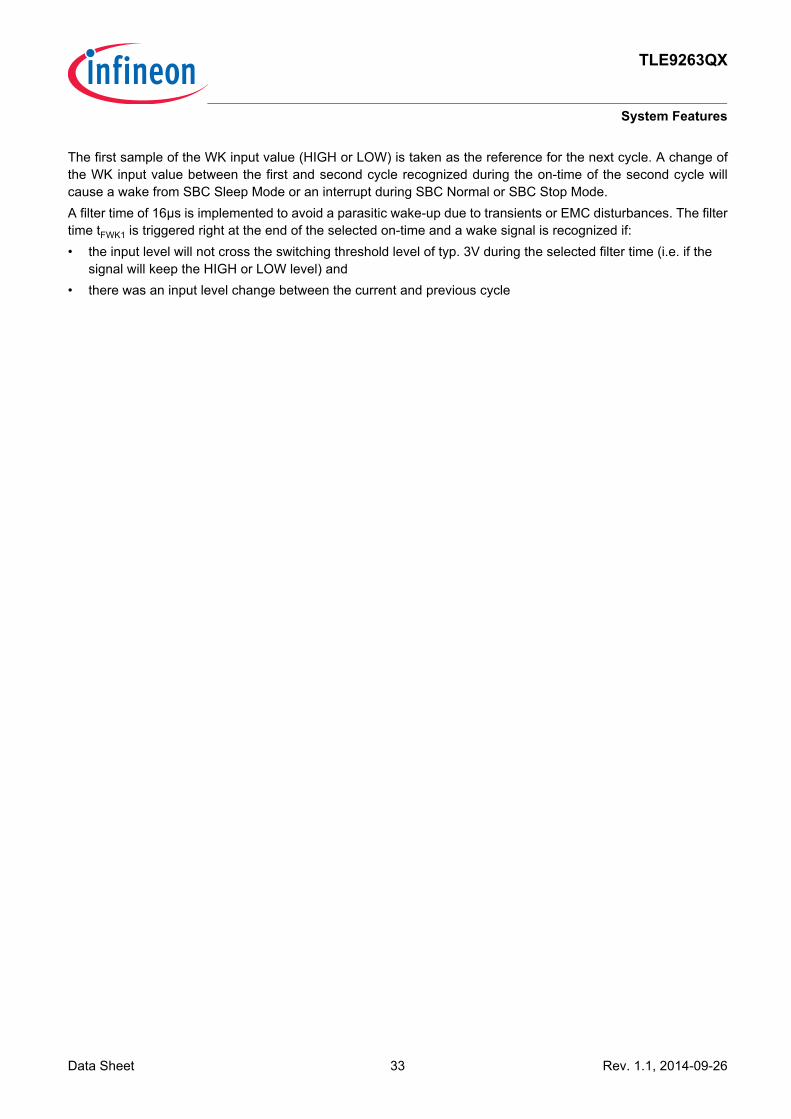
The first sample of the WK input value (HIGH or LOW) is taken as the reference for the next cycle. A change ofthe WK input value between the first and second cycle recognized during the on-time of the second cycle willcause a wake from SBC Sleep Mode or an interrupt during SBC Normal or SBC Stop Mode. A filter time of 16µs is implemented to avoid a parasitic wake-up due to transients or EMC disturbances. The filtertime tFWK1 is triggered right at the end of the selected on-time and a wake signal is recognized if:• the input level will not cross the switching threshold level of typ. 3V during the selected filter time (i.e. if the
signal will keep the HIGH or LOW level) and• there was an input level change between the current and previous cycle

TLE9263QX
System Features
Data Sheet 34 Rev. 1.1, 2014-09-26
A wake event due to cyclic sense in SBC Mode will set the respective bit WK1_WU, WK2_WU, or WK3_WU.During Cyclic Sense, WK_LVL_STAT is updated only with the sampled voltage levels of the WKx pins in SBCNormal or SBC Stop Mode.The functionality of the sampling and different scenarios are depicted in Figure 7 to Figure 9. The behavior in SBCStop and SBC Sleep Mode is identical except that in Stop Mode INT will be triggered to signal a change of WKinput levels and in SBC Sleep Mode, VCC1 will power-up instead.
Figure 7 Wake Input Timing
Figure 8 Cyclic Sense Example in SBC Stop Mode, HSx starts “OFF”/LOW, GND based WKx input
Filter timetFWK1
On Time
PeriodeHS switch
t
Filter timetFWK1
HS on Cyclic Sense
1st sample taken as reference
Wake detection possible on 2nd sample
High
n-1
Low
open
closed
Filter time
INT & WK Bit Set
LearningCycle
WKn-1= High
WKn= LowWKn ≠WKn-1
wake event
WKn+1 = LowWKn = WKn+1 no wake
WKn+2= HighWKn+2 ≠WKn+1
wake event
n n+1 n+2
HS
WKHigh
Low
Switch
INTHigh
Low
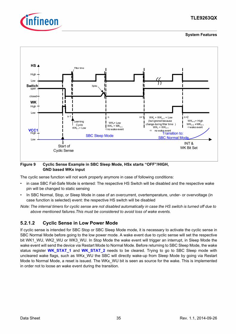
TLE9263QX
System Features
Data Sheet 35 Rev. 1.1, 2014-09-26
Figure 9 Cyclic Sense Example in SBC Sleep Mode, HSx starts “OFF”/HIGH, GND based WKx input
The cyclic sense function will not work properly anymore in case of following conditions:• in case SBC Fail-Safe Mode is entered: The respective HS Switch will be disabled and the respective wake
pin will be changed to static sensing• In SBC Normal, Stop, or Sleep Mode in case of an overcurrent, overtemperature, under- or overvoltage (in
case function is selected) event: the respective HS switch will be disabledNote: The internal timers for cyclic sense are not disabled automatically in case the HS switch is turned off due to
above mentioned failures.This must be considered to avoid loss of wake events.
5.2.1.2 Cyclic Sense in Low Power ModeIf cyclic sense is intended for SBC Stop or SBC Sleep Mode mode, it is necessary to activate the cyclic sense inSBC Normal Mode before going to the low power mode. A wake event due to cyclic sense will set the respectivebit WK1_WU, WK2_WU or WK3_WU. In Stop Mode the wake event will trigger an interrupt, in Sleep Mode thewake event will send the device via Restart Mode to Normal Mode. Before returning to SBC Sleep Mode, the wakestatus register WK_STAT_1 and WK_STAT_2 needs to be cleared. Trying to go to SBC Sleep mode withuncleared wake flags, such as WKx_WU the SBC will directly wake-up from Sleep Mode by going via RestartMode to Normal Mode, a reset is issued. The WKx_WU bit is seen as source for the wake. This is implementedin order not to loose an wake event during the transition.
Start of Cyclic Sense
High
n-1
Low
open
closed
Filter time
INT & WK Bit Set
LearningCycle
WKn-1= Low
WKn= LowWKn = WKn-1
no wake event
WKn = WKn+1 = Low (but ignored because
change during filter time )WKn = WKn+1
no wake event
WKn+2= HighWKn+2 ≠WKn+1
wake event
n n+1 n+2
HS
WKHigh
Low
Switch
High
Low
VCC1SBC Sleep Mode
Spike
Transition to:SBC Normal Mode

TLE9263QX
System Features
Data Sheet 36 Rev. 1.1, 2014-09-26
5.2.2 Cyclic WakeThe cyclic wake feature is intended to reduce the quiescent current of the device and application.For the cyclic wake feature one or both timers are configured as internal wake-up source and will periodicallytrigger an interrupt in SBC Normal and SBC Stop Mode. The correct sequence to configure the cyclic wake is shown in Figure 10. The sequence is as follows:• First, disable the timers to ensure that there is not unintentional interrupt when activating cyclic wake,• Enable Timer1 and/or Timer2 as a wake-up source in the register WK_CTRL_1,• Configure the respective period Timer1 and/or Timer2. Also an on-time (any value) must be selected to start
the cyclic wake even if the value is ignored.
Figure 10 Cyclic Wake: Configuration and Sequence
As in cyclic sense, the cyclic wake function will start as soon as the on-time is configured. An interrupt is generatedfor every start of the on time except for the very first time when the timer is started
Cyclic Wake Configuration
Cyclic Wake starts / ends by setting / clearing On-time
INT is pulled low at every rising edge of On-time except first one
Select Timer Period and any On-Time in TIMERX_CTRL
Periods : 10, 20, 50, 100, 200ms, 1s, 2sOn-times: any
(OFF/LOW & OFF/HIGH are not allowed )
Disable Timer1 and/or Timer2 as a wake source in WK_CTRL_1 To avoid unintentional interrupts
Select Timer1 and/or Timer2 as a wake source in WK_CTRL_1
No interrupt will be generated , if the timer is not enabled as a wake source
TLE9263QX
System Features
Data Sheet 37 Rev. 1.1, 2014-09-26
5.2.3 Internal TimerThe integrated Timer1 and Timer2 are typically used to wake up the microcontroller periodically (cyclic wake) orto perform cyclic sense on the wake inputs. Therefore, the timers can be mapped to the dedicated HS switchesby SPI (via HS_CTRL1...2).Following periods and on-times can be selected via the register TIMER1_CTRL and TIMER2_CTRL respectively: • Period: 10ms / 20ms / 50ms / 100ms / 200ms / 1s / 2s • On time: 0.1ms / 0.3ms / 1.0ms / 10ms / 20ms / OFF at HIGH or LOW
5.3 Supervision FeaturesThe device offers various supervision features to support functional safety requirements. Please see Chapter 15for more information.
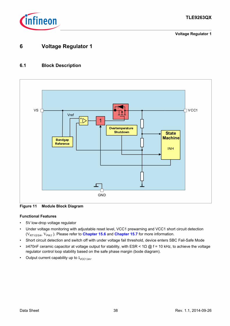
Data Sheet 38 Rev. 1.1, 2014-09-26
TLE9263QX
Voltage Regulator 1
6 Voltage Regulator 1
6.1 Block Description
Figure 11 Module Block Diagram
Functional Features• 5V low-drop voltage regulator• Under voltage monitoring with adjustable reset level, VCC1 prewarning and VCC1 short circuit detection
(VRT1/2/3/4, VPW,f ). Please refer to Chapter 15.6 and Chapter 15.7 for more information.• Short circuit detection and switch off with under voltage fail threshold, device enters SBC Fail-Safe Mode• ≥470nF ceramic capacitor at voltage output for stability, with ESR < 1Ω @ f = 10 kHz, to achieve the voltage
regulator control loop stability based on the safe phase margin (bode diagram).• Output current capability up to IVCC1,lim.
GND
OvertemperatureShutdown
1
BandgapReference
VS
StateMachine
VCC1
INH
Vref

Data Sheet 39 Rev. 1.1, 2014-09-26
TLE9263QX
Voltage Regulator 1
6.2 Functional DescriptionThe Voltage Regulator 1 (=VCC1) is “ON” in SBC Normal and SBC Stop Mode and is disabled in SBC Sleep andin SBC Fail-Safe Mode. The regulator can provide an output current up to IVCC1,lim.For low-quiescent current reasons, the output voltage tolerance is decreased in SBC Stop Mode because only alow-power mode regulator with a lower accuracy (VCC1,out41) will be active for small loads. If the load current onVCC1 exceeds the selected threshold (IVCC1,Ipeak1,r or IVCC1,Ipeak2,r) then the high-power mode regulator will be alsoactivated to support an optimum dynamic load behavior. The current consumption will then increase by typ. 2.9mA. If the load current on VCC1 falls below the selected threshold (IVCC1,Ipeak1,f or IVCC1,Ipeak2,f), then the low-quiescentcurrent mode is resumed again by disabling the high-power mode regulator. Both regulators (low-power mode and high-power mode) are active in SBC Normal Mode.Two different active peak thresholds can be selected via SPI:• I_PEAK_TH = ‘0’(default): the lower VCC1 active peak threshold 1 is selected with lowest quiescent current
consumption in SBC Stop Mode (IStop_1,25, IStop_1,85);• I_PEAK_TH = ‘1’: the higher VCC1 active peak threshold 2 is selected with an increased quiescent current
consumption in SBC Stop Mode (IStop_2,25, IStop_2,85);

Data Sheet 40 Rev. 1.1, 2014-09-26
TLE9263QX
Voltage Regulator 1
6.3 Electrical Characteristics
Table 9 Electrical CharacteristicsVS = 5.5 V to 28 V; Tj = -40 °C to +150 °C; all voltages with respect to ground, positive current flowing into pin (unless otherwise specified)Parameter Symbol Values Unit Note / Test Condition Number
Min. Typ. Max.Output Voltage including line and Load regulation
VCC1,out1 4.9 5.0 5.1 V 1)SBC Normal Mode; 10µA < IVCC1 < 250mA6V < VS < 28V
1) In SBC Stop Mode, the specified output voltage tolerance applies when IVCC1 has exceeded the selected active peak threshold (IVCC1,Ipeak1,r or IVCC1,Ipeak2,r) but with increased current consumption.
P_6.3.1
Output Voltage including line and Load regulation
VCC1,out2 4.9 5.0 5.1 V 1)SBC Normal Mode; 10µA < IVCC1 < 150mA
P_6.3.7
Output Voltage including line and Load regulation
VCC1,out3 4.97 – 5.07 V 1)2)SBC Normal Mode; 20mA < IVCC1 < 90mA 8V < VS < 18V25°C < Tj < 125°C
P_6.3.12
Output Voltage including line and Load regulation
VCC1,out41 4.9 5.05 5.2 V SBC Stop Mode;1mA < IVCC1 < IVCC1,Ipeak
P_6.3.2
Output Voltage including line and Load regulation
VCC1,out42 4.9 5.05 5.25 V SBC Stop Mode;10µA < IVCC1 < 1mA
P_6.3.20
Output Drop VCC1,d1 – – 500 mV IVCC1 = 50mA VS=3V
P_6.3.3
Output Drop VCC1,d2 – – 500 mV IVCC1 = 150mA VS=5V
P_6.3.4
VCC1 Active Peak Threshold 1 (Transition threshold between low-power and high-power mode regulator)
IVCC1,Ipeak1,r – 1.9 3.5 mA 2) ICC1 rising; VS = 13.5V -40°C < Tj < 150°C; I_PEAK_TH = ‘0’
2) Not subject to production test, specified by design.
P_6.3.13
VCC1 Active Peak Threshold 1 (Transition threshold between high-power and low-power mode regulator)
IVCC1,Ipeak1,f 0.5 1.3 – mA 2) ICC1 falling; VS = 13.5V -40°C < Tj < 150°C; I_PEAK_TH = ‘0’
P_6.3.17
VCC1 Active Peak Threshold 2 (Transition threshold between low-power and high-power mode regulator)
IVCC1,Ipeak2,r – 4.3 7.0 mA 2) ICC1 rising; VS = 13.5V -40°C < Tj < 150°C;I_PEAK_TH = ‘1’
P_6.3.18
VCC1 Active Peak Threshold 2 (Transition threshold between high-power and low-power mode regulator)
IVCC1,Ipeak2,f 1.7 3.4 – mA 2) ICC1 falling; VS = 13.5V -40°C < Tj < 150°C;I_PEAK_TH = ‘1’
P_6.3.19
Over Current Limitation IVCC1,lim 250 – 12002) mA current flowing out of pin, VCC1 = 0V
P_6.3.6

Data Sheet 41 Rev. 1.1, 2014-09-26
TLE9263QX
Voltage Regulator 1
Figure 12 Typical on-resistance of VCC1 pass device during low drop operation for ICC1 = 100mA

Data Sheet 42 Rev. 1.1, 2014-09-26
TLE9263QX
Voltage Regulator 1
Figure 13 On-resistance range of VCC1 pass device during low drop operation for ICC1 = 150mA

Data Sheet 43 Rev. 1.1, 2014-09-26
TLE9263QX
Voltage Regulator 2
7 Voltage Regulator 2
7.1 Block Description
Figure 14 Module Block Diagram
Functional Features• 5 V low-drop voltage regulator• Protected against short to battery voltage, e.g. for off-board sensor supply• Can also be used for CAN supply• VCC2 under voltage monitoring. Please refer to Chapter 15.8 for more information• Can be active in SBC Normal, SBC Stop, and SBC Sleep Mode (not SBC Fail-Safe Mode)• VCC2 switch off after entering SBC Restart Mode. Switch off is latched, LDO must be enabled via SPI after
shutdown.• Over temperature protection• ≥ 470nF ceramic capacitor at output voltage for stability, with ESR < 1Ω @ f = 10 kHz, to achieve the voltage
regulator control loop stability based on the safe phase margin (bode diagram).• Output current capability up to IVCC2,lim.
GND
OvertemperatureShutdown
1
BandgapReference
VS
StateMachine
VCC2
INH
Vref

Data Sheet 44 Rev. 1.1, 2014-09-26
TLE9263QX
Voltage Regulator 2
7.2 Functional DescriptionIn SBC Normal Mode VCC2 can be switched on or off via SPI.For SBC Stop- or Sleep Mode, the VCC2 has to be switched on or off before entering the respective SBC mode.The regulator can provide an output current up to IVCC2,lim. For low-quiescent current reasons, the output voltage tolerance is decreased in SBC Stop Mode because only alow-power mode regulator with a lower accuracy (VCC2,out5) will be active for small loads. If the load current onVCC2 exceeds IVCC2 > IVCC2,Ipeak,r then the high-power mode regulator will also be enabled to support an optimumdynamic load behavior. The current consumption will then increase by typ. 2.9mA. If the load current on VCC2 falls below the threshold (IVCC2 < IVCC2,Ipeak,f), then the low-quiescent current mode isresumed again by disabling the high-power mode regulator. Both regulators are active in SBC Normal Mode.
Note: If the VCC2 output voltage is supplying external off-board loads, the application must consider the series resonance circuit built by cable inductance and decoupling capacitor at the load. Sufficient damping must be provided.
7.2.1 Short to Battery ProtectionThe output stage is protected for short to VBAT.

Data Sheet 45 Rev. 1.1, 2014-09-26
TLE9263QX
Voltage Regulator 2
7.3 Electrical Characteristics
Table 10 Electrical CharacteristicsVS = 5.5 V to 28 V; Tj = -40 °C to +150 °C; all voltages with respect to ground, positive current flowing into pin (unless otherwise specified)Parameter Symbol Values Unit Note / Test Condition Number
Min. Typ. Max.Output Voltage including line and Load regulation (SBC Normal Mode)
VCC2,out1 4.9 5.0 5.1 V 1)SBC Normal Mode; 10µA < IVCC2 < 100mA6.5V < VS < 28V
1) In SBC Stop Mode, the specified output voltage tolerance applies when IVCC2 has exceeded the selected active peak threshold (IVCC2,Ipeak,r) but with increased current consumption.
P_7.3.1
Output Voltage including line and Load regulation (SBC Normal Mode)
VCC2,out2 4.9 5.0 5.1 V 1)SBC Normal Mode; 10µA < IVCC2 < 80mA6V < VS < 28V
P_7.3.16
Output Voltage including line and Load regulation (SBC Normal Mode)
VCC2,out3 4.9 5.0 5.1 V 1)SBC Normal Mode; 10µA < IVCC2 < 40mA
P_7.3.2
Output Voltage including line and Load regulation (SBC Normal Mode)
VCC2,out4 4.97 – 5.07 V 2)SBC Normal Mode; 10µA < IVCC2 < 5mA8V < VS < 18V25°C < Tj < 125°C
2) Not subject to production test, specified by design.
P_7.3.14
Output Voltage including line and Load regulation (SBC Stop/Sleep Mode)
VCC2,out5 4.9 5.05 5.2 V Stop, Sleep Mode;1mA < IVCC2 < IVCC2,Ipeak
P_7.3.3
Output Voltage including line and Load regulation (SBC Stop/Sleep Mode)
VCC2,out6 4.9 5.05 5.25 V Stop, Sleep Mode;10µA < IVCC2 < 1mA
P_7.3.18
Output Drop VCC2,d1 – – 500 mV IVCC2 = 30mA VS = 5V
P_7.3.4
VCC2 Active Peak Threshold (Transition threshold between low-power and high-power mode regulator)
IVCC2,Ipeak,r – 1.9 3.5 mA 2)ICC2 rising; VS = 13.5V -40°C < Tj < 150°C
P_7.3.15
VCC2 Active Peak Threshold (Transition threshold between high-power and low-power mode regulator)
IVCC2,Ipeak,f 0.5 1.3 – mA 2)ICC2 falling; VS = 13.5V -40°C < Tj < 150°C
P_7.3.17
Over Current limitation IVCC2,lim 100 – 7502) mA current flowing out of pin, VCC2 = 0V
P_7.3.5

Data Sheet 46 Rev. 1.1, 2014-09-26
TLE9263QX
Voltage Regulator 2
Figure 15 Typical on-resistance of VCC2 pass device during low drop operation for ICC2 = 30mA

Data Sheet 47 Rev. 1.1, 2014-09-26
TLE9263QX
Voltage Regulator 2
Figure 16 On-resistance range of VCC2 pass device during low drop operation for ICC2 = 50mA

Data Sheet 48 Rev. 1.1, 2014-09-26
TLE9263QX
External Voltage Regulator 3
8 External Voltage Regulator 3
8.1 Block Description
Figure 17 Functional Block Diagram
Functional Features• 5V / 3.3V low-drop voltage regulator with external PNP transistor (up to 350mA with 470mΩ shunt resistor)• Four high-voltage pins are used: VS, VCC3B, VCC3SH, VCC3REF• Configurable as stand-alone regulator (5V or 3.3V output voltage selectable via SPI) or in load-sharing mode
with VCC1 (5V output voltage)• ≥ 4.7µF ceramic capacitor at output voltage for stability, with ESR < 150mΩ @ f = 10 kHz to achieve the voltage
regulator control loop stability based on the safe phase margin (bode diagram).• Overcurrent limitation with external shunt in stand-alone configuration• Adjustable load current sharing ratio between VCC1 and VCC3 for load-sharing configuration• Under voltage shutdown in stand-alone configuration only
Table 11 1)External Voltage Regulator Configurations depending on VCC1 output voltage
1) This settings are valid only for the VCC3 stand-alone configuration. The bit VCC3_ V_CFG is ignored for VCC3 load sharing configuration
VCC1 configuration VCC3 voltage for VCC3_ V_CFG = 0 VCC3 voltage for VCC3_ V_CFG = 1VCC1 = 5.0V VCC3 = 5.0V VCC3 = 3.3V
RBE
VS - VCC3shunt> Vshunt_threshold
VREFState Machine
+
-
ICC3base
VCC3REFVCC3BVCC3SHVS

Data Sheet 49 Rev. 1.1, 2014-09-26
TLE9263QX
External Voltage Regulator 3
8.2 Functional DescriptionThe external voltage regulator can be used as an independent voltage regulator or in load-sharing mode withVCC1. Setting VCC3_ON in the M_S_CTRL register in SBC Normal Mode sets the stand-alone configuration ofVCC3 as an independent voltage regulator. The load sharing configuration is set via the SPI bit VCC3_LS in theHW_CTRL register.
Figure 18 Selecting the Configuration of the VCC3 Regulator
Depending on the configuration the regulator will act in the respective SBC Mode as described in Table 12. Afterthe VCC3 configuration has been selected, it cannot be changed anymore.In stand-alone configuration the maximum current ICC3max is defined by the current limitation determined by theused shunt. In load sharing configuration, the shunt is used to determine the current ratio between VCC1 andVCC3. Since the junction temperature of the external PNP transistor cannot be sensed by the SBC, it cannot beprotected against over temperature by the SBC. Therefore the thermal behavior has to be analyzed by theapplication.For low-quiescent current reasons, the output voltage tolerance is decreased in SBC Stop Mode because a low-power mode regulator with a lower accuracy will be active for small loads. If the base current on VCC3 exceedsIVCC3base > IVCC3base,Ipeak,r then the high-power mode regulator is enabled additionally to support an optimumdynamic load behavior. If the base current on VCC3 falls below the threshold (IVCC3base < IVCC3base,Ipeak,f), then thelow-quiescent current consumption is resumed again by disabling the high-power mode regulator. Only the high-power mode regulator is active in SBC Normal Mode.The status of VCC3 is reported in the SUP_STAT_2 SPI register. The regulator will switch OFF in case of VSdropping below VS_UV regardless of the VCC3 configuration and will be automatically enabled again whenexceeding this threshold voltage unless the control bit VCC3_VS_ UV_OFF is set. VCC3 will also stay active inSBC Stop Mode when the bit VCC3_LS_ STP_ON is set and when load sharing is configured (for detailedprotection features see Chapter 15.7 and Chapter 16.3).
Set bitVCC3_V_CFG = 0
Set bitVCC3_ON = 0 or 1
Set bitVCC3_LS = 1
VCC3_V_CFG is automatically set to 0
VCC3_LS, VCC3_ON and VCC3_V_CFG cannot be
changed anymore VCC3_LS and VCC3_V_CFG cannot be changed anymore
(once VCC3_ON is set for the first time)
VCC3 load sharing?Default value of VCC3_LS = ‘0'
VCC3 output voltage in stand-aloneconfiguration
Set bitVCC3_V_CFG = 1
Set bitVCC3_ON = 0 or 1
stand-aloneconfiguration
VCC3 = 5V
stand-aloneconfiguration VCC3 = 3.3V
VCC3 load sharingVCC3 = VCC1
No
Yes 5.0V
3.3V

Data Sheet 50 Rev. 1.1, 2014-09-26
TLE9263QX
External Voltage Regulator 3
Note: The configuration of the VCC3 voltage regulator behavior must be done immediately after power-up of the
device and cannot be changed afterwards as long as the device is supplied.
Note: As soon as the bit VCC3_ON or VCC3_LS is set for the first time, the configuration for VCC3 cannot be changed anymore. This configuration is valid - also after a SBC Soft Reset - as long as the SBC is powered.
Note: If the VCC3 output voltage is supplying external off-board loads, the application must consider the series resonance circuit built by cable inductance and decoupling capacitor at the load. Sufficient damping must be provided (e.g. a 100Ohm resistor between the PNP collector and VCC3REF with 10uF capacitor on collector - see also Figure 19).
8.2.1 External Voltage Regulator as Independent Voltage RegulatorConfigured as an independent voltage regulator the SBC offers with VCC3 a third supply which could be used asoff-board supply e.g. for sensors due to the integrated HV pins VCC3B, VCC3SH, VCC3REF. This configuration is set and locked by enabling VCC3_ON while keeping VCC3_LS = 0. VCC3 can be switchedON or OFF but the configuration cannot be changed anymore. However, the SPI_FAIL is not set while trying tochange the configuration.An over current limitation function is realized with the external shunt (see Chapter 8.4 for calculating the desiredshunt value) and the output current shunt voltage threshold (Vshunt_threshold). If this threshold is reached, then ICC3is limited and only the current limitation bit VCC3_OC is set (no other reaction) and can be cleared via SPI oncethe over current condition is not present anymore. If the over current limitation feature is not needed, then connectthe pins VCC3SH and VS together. In this configuration VCC3 has the under voltage signalization enabled and an under voltage event is signaled withthe bit VCC3_UV in the SUP_STAT_2 SPI register.Note: To avoid undesired current consumption increase of the device it must be ensured that VCC3 is not
connected to VCC1 in this configuration.
Table 12 External Voltage Regulator State by SBC ModeSBC Mode Load Sharing Mode1)
1) Behaves as VCC1 and has to be configured in SBC Normal Mode
Independent Voltage RegulatorINIT Mode OFF OFF Normal Mode Configurable ConfigurableStop Mode OFF/Fixed2)
2) Load Sharing operation in SBC Stop Mode is by default disabled for power saving reasons but VCC3_LS bit will stay set. However, it can be also configured via the SPI bit VCC3_LS_ STP_ON to stay enabled in SBC Stop Mode.
FixedSleep Mode OFF FixedRestart Mode ON or ramping FixedFail-Safe Mode OFF OFF

Data Sheet 51 Rev. 1.1, 2014-09-26
TLE9263QX
External Voltage Regulator 3
Figure 19 Protecting the VCC3 against inductive short circuits when configured as an independent voltage regulator for off-board supply
8.2.2 External Voltage Regulator in Load Sharing ModeThe purpose of the load sharing mode is to increase the total current capability of VCC1 without increase of thepower dissipation within the SBC. The load current is shared between the VCC1 internal regulator and the externalPNP transistor of VCC3. Figure 20 shows the setup for Load Sharing. Load Sharing is active in SBC NormalMode. It can also be configured via SPI to stay active in SBC Stop Mode.An input voltage up to VSx,MAX is regulated to VCC3,nom = 5.0 V with a precision of ±2% when used in the load sharingconfiguration in SBC Normal Mode. This configuration is set and locked by enabling VCC3_LS for the first time while VCC3_ON has no function, i.e.keep VCC3_ON = 0. Trying to change the VCC3 configuration after VCC3_LS has been set will result in theSPI_FAIL bit being set and keeping the VCC3 configurations unchanged. Load sharing will be automaticallydisabled (only if VCC3_LS_ STP_ON = 0) during SBC Stop Mode due to power saving reasons but the bit willremain set to automatically switch back on after returning to SBC Normal Mode. It must be ensured that the sameVCC3 output voltage level is selected as for VCC1.In this configuration VCC3 has no undervoltage signalization. VCC3 shuts down if Fail-Safe Mode is reached, e.g. due to undervoltage shutdown (VS,UV monitoring).VCC3 has no over current limitation in this configuration and the shunt resistor is defining the load sharing ratiobetween the VCC1 and VCC3 load currents (see Equation (2) in Chapter 8.4). Thus, no over current conditionVCC3_OC will be signaled in this configuration.
RBE
VS - VCC3shunt> Vshunt_threshold
VREFState Machine
+
-
ICC3base
VCC3REFVCC3BVCC3SHVS
RSHUNT T1
C2C1
VS VCC3
ICC3
RLim
100 Ω

Data Sheet 52 Rev. 1.1, 2014-09-26
TLE9263QX
External Voltage Regulator 3
Figure 20 VCC3 in Load Sharing Configuration
8.3 External ComponentsCharacterization is performed with the BCP52-16 from Infineon (ICC3 < 200 mA) and with MJD253.Other PNP transistors can be used. However, the functionality must be checked in the application.Figure 20 shows one hardware set up used.
Note: The SBC is not able to ensure a thermal protection of the external PNP transistor. The power handling capabilities for the application must therefore be chosen according to the selected PNP device, the PCB layout and properties of the application to prevent thermal damage, e.g. via the shunt current limitation in stand alone configuration or by selecting the proper ICC1/ICC3 ratio in load-sharing configuration.
Note: To ensure an optimum EMC behavior of the VCC3 regulator when the VCC3 output is leaving the PCB, it is necessary to optimize the PCB layout to have the PNP very close to the SBC. If this is not sufficient or possible, an external capacitance should be placed to the off-board connector (see also Chapter 17.1).
Table 13 Bill of Materials for the VCC3 Function with and without load sharing configurationDevice Vendor Reference / ValueC2 Murata 10 µF/10 V GCM31CR71A106K64LRSHUNT - 1 Ω (with / without LS)T1 Infineon BCP52-16
VCC3REFVCC3BVCC3SHVS
RSHUNT T1
C2C1
VS VCC13
Vcc3
Vcc1
ICC3
ICC1

Data Sheet 53 Rev. 1.1, 2014-09-26
TLE9263QX
External Voltage Regulator 3
8.4 Calculation of RSHUNTAs a independent regulator, the maximum current ICC3max where the limit starts and the bit ICC3 > ICC3max is set isdetermined by the shunt resistor RSHUNT and the Output Current Shunt Voltage Threshold Vshunt_threshold.The resistor can be calculated as following:
(1)
If VCC3 is configured for load sharing, then the shunt resistor determines the load sharing ratio between VCC1and VCC3. The ratio can be calculated as following:
(2)
Example: A shunt resistor with 470mΩ and a load current of 100mA out of VCC1 would result in ICC3 = 191mA.
8.5 Unused PinsIn case the VCC3 is not used in the application, it is recommended to connect the unused pins of VCC3 asfollowed:• Connect VCC3SH to VS or leave open;• Leave VCC3B open;• Leave VCC3REF open• Do not enable the VCC3 via SPI as this leads to increased current consumption
max3
_
CC
thresholdshuntSHUNT I
UR =
)(15105110 1
1
3 aR
ImVII
SHUNT
CC
CC
CC −Ω=
)(1510511013 b
RmVII
SHUNT
CCCC
−Ω⋅=

Data Sheet 54 Rev. 1.1, 2014-09-26
TLE9263QX
External Voltage Regulator 3
8.6 Electrical CharacteristicsVS = 5.5 V to 28 V; Tj = -40 °C to +150 °C; SBC Normal Mode; all outputs open; all voltages with respect to ground;positive current defined flowing into pin; unless otherwise specified.
Table 14 Electrical CharacteristicsParameter Symbol Values Unit Note / Test Condition Number
Min. Typ. Max.Parameters independent from Test Set-upExternal Regulator Control Drive Current Capability
IVCC3base 40 60 80 mA VVCC3base = 13.5 V P_8.6.1
Input Current VCC3ref IVCC3ref 0 3 10 µA VVCC3ref = 5 V P_8.6.2
Input Current VCC3 Shunt Pin
IVCC3shunt 0 3 10 µA VVCC3shunt = VS P_8.6.3
Output Current Shunt Voltage Threshold
Vshunt_threshold 180 245 310 mV 1) P_8.6.6
Current increase regulation reaction time
trIinc – – 5 µs 4)VCC3 = 6 V to 0 V;ICC3base = 20 mA Figure 21
P_8.6.7
Current decrease regulation reaction time
trIdec – – 5 µs 4)VCC3 = 0 V to 6 V;ICC3base = 20 mA Figure 21
P_8.6.8
Leakage current of VCC3base when VCC3 disabled
IVCC3base_lk – – 5 µA VCC3base = VS;Tj = 25°C
P_8.6.9
Leakage current of VCC3shunt when VCC3 disabled
IVCC3shunt_lk – – 5 µA VCC3shunt = VS;Tj = 25°C
P_8.6.11
Base to emitter resistor RBE 120 150 185 kΩ VCC3 = OFF; P_8.6.12
Active Peak Threshold VCC3 (Transition threshold between low-power and high-power mode regulator)
IVCC3base,Ipeak,r – 50 65 µA 4)Drive current IVCC3base; IVCC3base risingVS =13.5V; -40°C < Tj < 150°C
P_8.6.33
Active Peak Threshold VCC3 (Transition threshold between high-power and low-power mode regulator)
IVCC3base,Ipeak,f 15 30 – µA 4)Drive current IVCC3base; IVCC3base fallingVS =13.5V; -40°C < Tj < 150°C
P_8.6.34
Parameters dependent on the Test Set-up (with external PNP device MJD-253)External Regulator Output Voltage (VCC3 = 5.0V)
VCC3.out1 4.9 5 5.1 V 2)SBC Normal Mode; load sharing configuration with 470 mΩ shunt resistor;10 µA < IVCC1 + IVCC3 < 300 mA;
P_8.6.13
External Regulator Output Voltage(VCC3 = 5.0V)
VCC3,out2 4.9 5 5.1 V 2)SBC Normal Mode;stand-alone configuration10 mA < IVCC3 < 300 mA;
P_8.6.14

Data Sheet 55 Rev. 1.1, 2014-09-26
TLE9263QX
External Voltage Regulator 3
External Regulator Output Voltage(VCC3 = 5.0V)
VCC3,out3 4.8 5 5.2 V 2)SBC Stop-, Sleep Mode;Stand-alone configuration10µA < IVCC3 < IVCC3_peak,r
3)
P_8.6.15
External Regulator Output Voltage(VCC3 = 3.3V)
VCC3,out4 3.23 3.3V 3.37 V 2)SBC Normal Mode;stand-alone configuration10 mA < IVCC3 < 300 mA;
P_8.6.22
External Regulator Output Voltage(VCC3 = 3.3V)
VCC3,out5 3.15 3.3V 3.45 V 2)SBC Stop-, Sleep Mode;Stand-alone configuration10µA < IVCC3 < IVCC3_peak,r
3)
P_8.6.23
Load Sharing Ratio ICC1 : ICC3
RatioLS_1,VCC3 1 : 1.35
1 : 1.9
1 : 2.45
– 4)5)6.0V < VS < 28V; SBC Normal Mode;LS ratio for a 470 mΩ shunt resistor and total load current of 300mA
P_8.6.16
Load Sharing Ratio ICC1 : ICC3
RatioLS_2,VCC3 1 : 0.67
1 : 0.95
1 : 1.23
– 4)5)6.0V < VS < 28V; SBC Normal Mode;LS ratio for a 1 Ω shunt resistor and total load current of 300mA
P_8.6.20
Load Sharing Ratio ICC1 : ICC3
RatioLS_3,VCC3 1 : 1.50
1 : 1.95
1 : 2.40
– 4)5) Tj = 150°C; 8.0V < VS < 18V; SBC Normal Mode;LS ratio for a 470 mΩ shunt resistor and total load current of 300mA
P_8.6.27
Load Sharing Ratio ICC1 : ICC3
RatioLS_4,VCC3 1 : 0.75
1 : 0.98
1 : 1.21
– 4)5) Tj = 150°C; 8.0V < VS < 18V; SBC Normal Mode;LS ratio for a 1 Ω shunt resistor and total load current of 300mA
P_8.6.28
1) Threshold at which the current limitation starts to operate. This threshold is only active when VCC3 is configured for stand-alone configuration.
2) Tolerance includes load regulation and line regulation.3) IVCC3_peak refers to the load current out of the collector of the external PNP device. This value can be calculated by
multiplying the VCC3base active peak threshold (IVCC3base,Ipeak) with the current gain of the PNP4) Not subject to production test, specified by design.5) a) Ratio will change depending on the chosen shunt resistor which value is correlating to the maximum power dissipation
of the PNP pass device. See Chapter 8.4 for the ratio calculation. The ratio will also change at low-drop operation. For supply voltages of 5.5V < VS < 6V the accuracy applies only for a total load current of 250mA.The load sharing ratio in SBC Stop Mode has +/-10% wider limits than specified.
b) The output voltage precision in load sharing in SBC Stop Mode is according to VCC1 +/-4% or better for loads up to 20mA and +/-2% with loads greater than 20mA. In SBC Normal the +/-2% precision for 5V/3.3V tolerance is valid regardless of the applied load.
Table 14 Electrical Characteristics (cont’d)
Parameter Symbol Values Unit Note / Test Condition NumberMin. Typ. Max.

Data Sheet 56 Rev. 1.1, 2014-09-26
TLE9263QX
External Voltage Regulator 3
Note: At Tj > 125°C, the power transistor leakage could be increased, which has to be added to the quiescent current of the application independently if the regulator is turned on/off. To prevent an over-voltage condition at no load due to this increased leakage, an internal clamping structure will automatically turn on at typ. 200mV above the upper limit of the programmed output voltage.
Note: There is no thermal protection available for the external PNP transistor. Therefore, the application must be designed to avoid overheating of the PNP via the shunt current limitation in stand alone configuration and by selecting the proper ICC1/ICC3 ratio in load-sharing configuration.
Note: In SBC Stop Mode, the same output voltage tolerance applies as in SBC Normal Mode when IVCC3 has exceeded the selected active peak threshold (IVCC3base,Ipeak) but with increased current consumption.

Data Sheet 57 Rev. 1.1, 2014-09-26
TLE9263QX
External Voltage Regulator 3
Timing diagram for regulator reaction time “current increase regulation reaction time” and “current decreaseregulation reaction time”
Figure 21 Regulator Reaction Time
t
t
VCC3
ICCbase
ICC3base, 50%
trlinc trldec

Data Sheet 58 Rev. 1.1, 2014-09-26
TLE9263QX
External Voltage Regulator 3
Typical Load Sharing Characteristics using the BCP52-16 PNP transistor and a 1 Ω shunt resistor
Figure 22 Load Sharing Ratio ICC1 : ICC3 vs. the total load current
Figure 23 Load Sharing Behavior of ICC1 vs. the total load current
0 0,2 0,4 0,6 0,8 1,0 1,2 1,40
0,05
0,10
0,15
0,20
0,25
0,30
0,35
Load Sharing Ratio - Icc1 vs. Icc3
Tot
al C
urre
nt -
Icc
1 +
Icc
3 (m
A)
Tj = 27°C
Tj = 150°C
Tj = -40°C
(A)
- Icc3 vs. Icc1
0 0,02 0,04 0,06 0,08 0,10 0,12 0,14 0,160
0,05
0,10
0,15
0,20
0,25
0,30
0,35
Load Current - Icc1
Tot
al C
urre
nt -
Icc
1 +
Icc
3 (m
A)
Tj = 27°C
Tj = 150°C
Tj = -40°C
(A)

Data Sheet 59 Rev. 1.1, 2014-09-26
TLE9263QX
High-Side Switch
9 High-Side Switch
9.1 Block Description
Figure 24 High-Side Module Block Diagram
Features• Dedicated supply pin VSHS for high-side outputs • Over voltage and under voltage switch off - configurable via SPI• Overcurrent detection and switch off• Open load detection in ON-state• PWM capability with internal timer configurable via SPI• Switch recovery after removal of OV or UV condition configurable via SPI
9.2 Functional DescriptionThe High-Side switches can be used for control of LEDs, as supply for the wake inputs and for other loads. TheHigh-Side outputs can be controlled either directly via SPI by (HS_CTRL1, HS_CTRL2), by the integrated timersor by the integrated PWM generators. The high-side outputs are supplied by a dedicated supply pin VSHS (different to VS). The topology supportsimproved cranking condition behavior.The configuration of the High-Side (Permanent On, PWM, cyclic sense, etc.) drivers must be done in SBC NormalMode. The configuration is taken over in SBC Stop- or SBC Sleep Mode and cannot be modified. When enteringSBC Restart Mode or SBC Fail-Safe Mode the HSx outputs are disabled.
HS Gate ControlOvercurrent Detection
Open Load (On)
VSHS
HSx

Data Sheet 60 Rev. 1.1, 2014-09-26
TLE9263QX
High-Side Switch
9.2.1 Over and Under Voltage Switch OffAll HS drivers in on-state are switched off in case of over voltage on VSHS (VSHS,OVD). If the voltage drops belowthe over voltage threshold the HS drivers are activated again. The feature can be disabled by setting the SPI bitHS_OV_SD_EN.The HS drivers are switched off in case of under voltage on VSHS (VSHS,UVD). If the voltage rises above the undervoltage threshold the HS drivers are activated again. The feature can be disabled by setting the SPI bitHS_UV_SD_EN.So after release of under voltage or over voltage condition the HS switch goes back to programmed state in whichit was configured via SPI. This behavior is only valid if the bit HS_OV_UV_REC is set to ‘1’. Otherwise the switcheswill stay off and the respective SPI control bits are cleared are cleared.The over voltage and under voltage is signaled in the bits VSHS_OV and VSHS_UV, no other error bits are set.
9.2.2 Over Current Detection and Switch OffIf the load current exceeds the over current shutdown threshold for a time longer then the over current shutdownfilter time the output is switched off.The over current condition and the switch off is signaled with the respective HSx_OC_OT bit in the registerHS_OC_OT_STAT. The HSx configuration is then reset to 000 by the SBC. To activate the High-Side again theHSx configuration has to be set to ON (001) or be programmed to a timer function. It is recommended to clear theover current bit before activation the High-Side switch, as the bits are not cleared automatically by the SBC.
9.2.3 Open Load DetectionOpen load detection on the High-Side outputs is done during on state of the output. If the current in the activatedoutput falls below then Open Load Detection current, the open load is detected and signaled via the respective bitHS1_OL, HS2_OL, HS3_OL, or HS4_OL in the register HS_OL_STAT. The High-Side output stays activated. Ifthe open load condition disappears the Open Load bit in the SPI can be cleared. The bits are not clearedautomatically by the SBC.
9.2.4 HSx Operation in Different SBC Modes
• During SBC Stop and SBC Sleep Mode the HSx outputs can be used for the cyclic sense feature. The open-load detection, over current shut down as well as over voltage and under voltage shutdown are available. The over current shutdown protection feature may influence the wake-up behavior1).
• the HSx output can also be enabled for SBC Stop and SBC Sleep Mode as well as controlled by the PWMx generator. The HSx outputs must be configured in SBC Normal Mode before entering a low-power mode.
• The HSx outputs are switched off during SBC Restart or SBC Fail-Safe Mode. They can be enabled via SPI if the failure condition is removed.
1) For the wake feature, the forced over current shut down case must be considered in the user software for all SBC Modes, i.e. due to disabled HSx switches a level change might not be detected anymore at WKx pins.

Data Sheet 61 Rev. 1.1, 2014-09-26
TLE9263QX
High-Side Switch
9.2.5 PWM and Timer Function
Two 8-bit PWM generators are dedicated to generate a PWM signal on the HS outputs, e.g. for brightnessadjustment or compensation of supply voltage fluctuation. The PWM generators are mapped to the dedicated HSoutputs, and the duty cycle can be independently configured with a 8bit resolution via SPI (PWM1_CTRL,PWM2_CTRL). Two different frequencies (200Hz, 400Hz) can be selected independently for every PWMgenerator in the register PWM_FREQ_CTRL.
PWM Assignment and Configuration:• Configure duty cycle and frequency for respective PWM generator in PWM1_CTRL/PWM2_CTRL and
PWM_FREQ_CTRL• Assign PWM generator to respective HS switch(es) in HSx_CTRL• The PWM generation will start right after the HSx is assigned to the PWM generator (HS_CTRL1, HS_CTRL2)
Assignment options of HS1... HS4• Timer 1 • Timer 2• PWM 1 • PWM 2Note: The min. On-time during PWM is limited by the actual Ton and Toff time of the respective HS switch, e.g.
the PWM setting ‘0000 0001’ could not be realized. In addition, the minimum PWM setting for reliable detection of over-current and open-load measurement is 4 digits for a period of 400Hz and 2 digits for a period of 200Hz
Data Sheet 62 Rev. 1.1, 2014-09-26
TLE9263QX
High-Side Switch
9.3 Electrical Characteristics
Table 15 Target SpecificationsVS = 5.5 V to 28 V; Tj = -40 °C to +150 °C; all voltages with respect to ground, positive current flowing into pin (unless otherwise specified)Parameter Symbol Values Unit Note /
Test ConditionNumber
Min. Typ. Max.Output HS1, HS2, HS3, HS4Static Drain-Source ON Resistance HS1...HS4
RON,HS25 – 7 – Ω Ids = 60mA,Tj < 25°C
P_9.3.1
Static Drain-Source ON Resistance HS1...HS4
RON,HS150 – 11.5 16 Ω Ids = 60mA, Tj < 150°C
P_9.3.2
Leakage Current HSx / per channel
Ileak,HS – – 2 µA 1)0 V < VHSx < VSHS;Tj < 85°C
P_9.3.11
Output Slew Rate (rising) SRraise,HS 0.8 – 2.5 V/µs 1)20 to 80%VSHS = 6 to 18VRL = 220Ω
1) Not subject to production test, specified by design.
P_9.3.3
Output Slew Rate (falling) SRfall,HS -2.5 – -0.8 V/µs 1)80 to 20%VSHS = 6 to 18VRL = 220Ω
P_9.3.4
Switch-on time HSx tON,HS 3 – 30 µs CSN = HIGH to 0.8*VSHS; RL = 220Ω; VSHS = 6 to 18V
P_9.3.5
Switch-off time HSx tOFF,HS 3 – 30 µs CSN = HIGH to 0.2*VSHS; RL = 220Ω; VSHS = 6 to 18V
P_9.3.6
Short Circuit Shutdown Current
ISD,HS 150 245 300 mA VSHS = 6 to 20V, hysteresis included
P_9.3.7
Short Circuit Shutdown Filter Time
tSD,HS 16 µs 2), 3)
2) Not subject to production test, tolerance defined by internal oscillator tolerance.3) The minimum PWM setting for reliable detection of over current and open load measurement is 5 digits for a period of
200Hz and 3 digits for a period of 150Hz.
P_9.3.8
Open Load Detection Current IOL,HS 0.4 – 3 mA hysteresis included
P_9.3.9
Open Load Detection hysteresis
IOL,HS,hys – 0.45 – mA 1) P_9.3.14
Open Load Detection Filter Time
tOL,HS – 64 – µs 2), 3) P_9.3.10

Data Sheet 63 Rev. 1.1, 2014-09-26
TLE9263QX
High Speed CAN Transceiver
10 High Speed CAN Transceiver
10.1 Block Description
Figure 25 Functional Block Diagram
10.2 Functional DescriptionThe Controller Area Network (CAN) transceiver part of the SBC provides high-speed (HS) differential mode datatransmission (up to 2 Mbaud) and reception in automotive and industrial applications. It works as an interfacebetween the CAN protocol controller and the physical bus lines compatible to ISO/DIS 11898-2, 11898-5 and SAEJ2284.The CAN transceiver offers low power modes to reduce current consumption. This supports networks with partiallypowered down nodes. To support software diagnostic functions, a CAN Receive-only Mode is implemented.It is designed to provide excellent passive behavior when the transceiver is switched off (mixed networks,clamp15/30 applications).A wake-up from the CAN wake capable mode is possible via a message on the bus. Thus, the microcontroller canbe powered down or idled and will be woken up by the CAN bus activities.The CAN transceiver is designed to withstand the severe conditions of automotive applications and to support12 V applications. The different transceiver modes can be controlled via the SPI CAN bits.
TXDCANOutput
Stage
Driver
Temp.-Protection
CANH
CANL +timeout
RXDCAN
Receiver
MUX
VCC1
SPI Mode Control
To SPI diagnostic
VCAN
VCC1
RTXD
Wake Receiver
Vs
VCAN
VBIAS = 2.5V
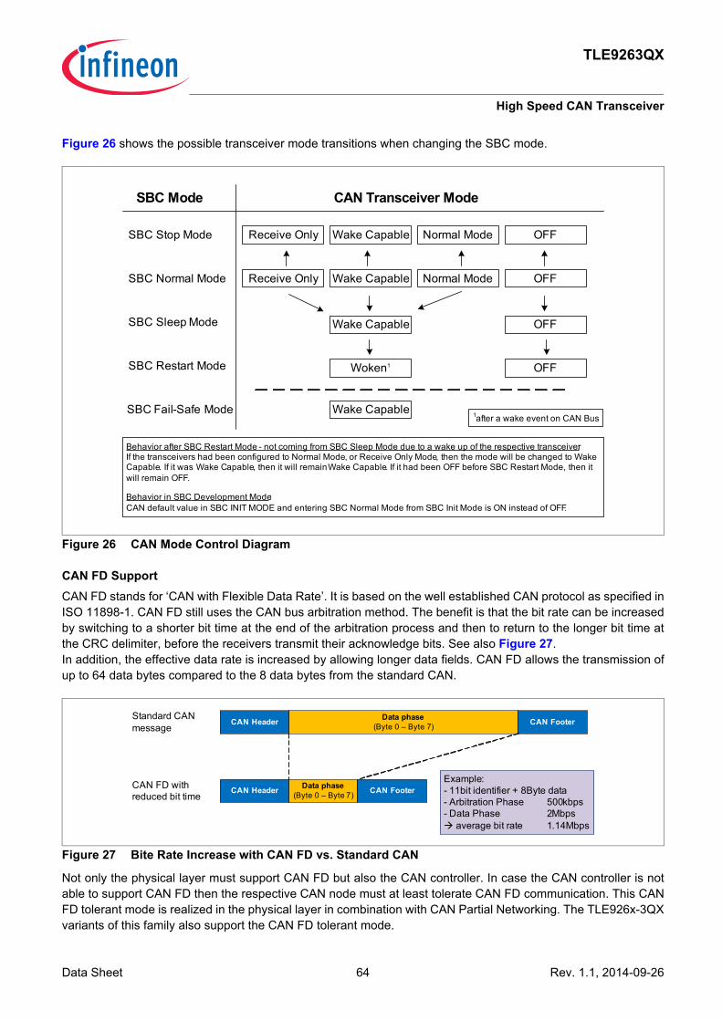
Data Sheet 64 Rev. 1.1, 2014-09-26
TLE9263QX
High Speed CAN Transceiver
Figure 26 shows the possible transceiver mode transitions when changing the SBC mode.
Figure 26 CAN Mode Control Diagram
CAN FD SupportCAN FD stands for ‘CAN with Flexible Data Rate’. It is based on the well established CAN protocol as specified inISO 11898-1. CAN FD still uses the CAN bus arbitration method. The benefit is that the bit rate can be increasedby switching to a shorter bit time at the end of the arbitration process and then to return to the longer bit time atthe CRC delimiter, before the receivers transmit their acknowledge bits. See also Figure 27. In addition, the effective data rate is increased by allowing longer data fields. CAN FD allows the transmission ofup to 64 data bytes compared to the 8 data bytes from the standard CAN.
Figure 27 Bite Rate Increase with CAN FD vs. Standard CAN
Not only the physical layer must support CAN FD but also the CAN controller. In case the CAN controller is notable to support CAN FD then the respective CAN node must at least tolerate CAN FD communication. This CANFD tolerant mode is realized in the physical layer in combination with CAN Partial Networking. The TLE926x-3QXvariants of this family also support the CAN FD tolerant mode.
SBC Normal Mode
SBC Mode CAN Transceiver Mode
SBC Stop Mode
SBC Sleep Mode
SBC Restart Mode
Receive Only Normal Mode OFFWake Capable
Receive Only OFFWake Capable
OFFWoken1
OFFWake Capable
1after a wake event on CAN Bus
Normal Mode
Behavior after SBC Restart Mode - not coming from SBC Sleep Mode due to a wake up of the respective transceiver: If the transceivers had been configured to Normal Mode, or Receive Only Mode, then the mode will be changed to Wake Capable. If it was Wake Capable, then it will remain Wake Capable. If it had been OFF before SBC Restart Mode, then it will remain OFF.
Behavior in SBC Development Mode: CAN default value in SBC INIT MODE and entering SBC Normal Mode from SBC Init Mode is ON instead of OFF.
SBC Fail-Safe Mode Wake Capable
Example:- 11bit identifier + 8Byte data- Arbitration Phase 500kbps- Data Phase 2Mbps
average bit rate 1.14Mbps
CAN Header Data phase(Byte 0 – Byte 7) CAN FooterStandard CAN
message
CAN Header Data phase(Byte 0 – Byte 7) CAN FooterCAN FD with
reduced bit time

Data Sheet 65 Rev. 1.1, 2014-09-26
TLE9263QX
High Speed CAN Transceiver
10.2.1 CAN OFF ModeThe CAN OFF Mode is the default mode after power-up of the SBC. It is available in all SBC Modes and is intendedto completely stop CAN activities or when CAN communication is not needed. The CANH/L bus interface acts asa high impedance input with a very small leakage current. In CAN OFF Mode, a wake-up event on the bus will beignored.
10.2.2 CAN Normal ModeThe CAN Transceiver is enabled via SPI in SBC Normal Mode. CAN Normal Mode is designed for normal datatransmission/reception within the HS-CAN network. The Mode is available in SBC Normal Mode and in SBC StopMode. The bus biasing is set to VCAN/2.
TransmissionThe signal from the microcontroller is applied to the TXDCAN input of the SBC. The bus driver switches the CANH/L output stages to transfer this input signal to the CAN bus lines.
Enabling sequenceThe CAN transceiver requires an enabling time tCAN,EN before a message can be sent on the bus. This means thatthe TXDCAN signal can only be pulled LOW after the enabling time. If this is not ensured, then the TXDCAN needsto be set back to HIGH (=recessive) until the enabling time is completed.Only the next dominant bit will be transmitted on the bus.Figure 28 shows different scenarios and explanations for CAN enabling.
Figure 28 CAN Transceiver Enabling Sequence
Reduced Electromagnetic EmissionTo reduce electromagnetic emissions (EME), the bus driver controls CANH/L slopes symmetrically.
ReceptionAnalog CAN bus signals are converted into digital signals at RXD via the differential input receiver.
t
VCANDIFF
tCAN,ENt
VTXDCAN
t
CAN Mode
CAN NORMAL
CAN OFF
CAN,ENt
recessive TXD level required bevor start of
transmission
tCAN, EN not ensured , no transmission on bus
CAN,ENt
Correct sequence , Bus is enabled after tCAN, EN
tCAN, EN not ensured , no transmission on bus
recessive TXDlevel required
Dominant
Recessive

Data Sheet 66 Rev. 1.1, 2014-09-26
TLE9263QX
High Speed CAN Transceiver
10.2.3 CAN Receive Only ModeIn CAN Receive Only Mode (RXD only), the driver stage is de-activated but reception is still operational. This modeis accessible by an SPI command in Normal Mode and in Stop Mode. The bus biasing is set to VCAN/2.
10.2.4 CAN Wake Capable ModeThis mode can be used in SBC Stop, Sleep, Restart and Normal Mode and it is used to monitor bus activities. It is automatically accessed in SBC Fail-Safe Mode. Both bus pins CANH/L are connected to GND via the inputresistors.A wake-up signal on the bus results in a change of behavior of the SBC, as described in Table 16. The pinsCANH/L are terminated to typ. 2.5V through the input resistors. As a wake-up signalization to the microcontroller,the RXD_CAN pin is set LOW and will stay LOW until the CAN transceiver is changed to any other mode. After awake-up event, the transceiver can be switched to CAN Normal Mode for communication via SPI.
As shown in Figure 29, a wake-up pattern is signaled on the bus by two consecutive dominant bus levels for atleast tWake1 (filter time t > tWake1), each separated by a recessive bus level of less than tWake2.
Figure 29 WUP detection following the definition in ISO 11898-5
IniBias off
1Bias off
2Bias off
3Bias on
4Bias on
WaitBias off
Bus recessive > tWAKE1
Bus dominant > tWAKE1
optional:tWAKE2 expired
Bus recessive > tWAKE1
Bus dominant > tWAKE1
Bus recessive > tWAKE1Bus dominant > tWAKE1
optional:tWAKE2 expired
tSilence expired ANDDevice in low-power mode
tSilence expired ANDdevice in low-power mode
Entering CAN Normal
or CAN Recive Only
Entering low-power mode , when selective wake-up
function is disabled or not supported

Data Sheet 67 Rev. 1.1, 2014-09-26
TLE9263QX
High Speed CAN Transceiver
Rearming the Transceiver for Wake CapabilityAfter a BUS wake-up event, the transceiver is woken. However, the CAN transceiver mode bits will still show wakecapable (=‘01’) so that the RXD signal will be pulled low. There are two possibilities how the CAN transceiver’swake capable mode is enabled again after a wake event:• The CAN transceiver mode must be toggled, i.e. switched from Wake Capable Mode to CAN Normal Mode,
CAN Receive Only Mode or CAN Off, before switching to CAN Wake Capable Mode again.• Rearming is done automatically when the SBC is changed to SBC Stop, SBC Sleep, or SBC Fail-Safe Mode
to ensure wake-up capability.Note: It is not necessary to clear the CAN wake-up bit CAN_WU to become wake capable again. It is sufficient to
toggle the CAN mode.
Note: The CAN module is supplied by an internal voltage when in CAN Wake Capable Mode, i.e. the module must not be supplied through the VCAN pin during this time. Before changing the CAN Mode to Normal Mode, the supply of VCAN has to be activated first.
Wake-Up in SBC Stop and Normal ModeIn SBC Stop Mode, if a wake-up is detected, it is always signaled by the INT output and in the WK_STAT_1 SPIregister. It is also signaled by RXDCAN pulled to low. The same applies for the SBC Normal Mode. Themicrocontroller should set the device from SBC Stop Mode to SBC Normal Mode, there is no automatic transitionto Normal Mode. For functional safety reasons, the watchdog will be automatically enabled in SBC Stop Mode after a Bus wakeevent in case it was disabled before (if bit WD_EN_ WK_BUS was configured to HIGH before).
Wake-Up in SBC Sleep ModeWake-up is possible via a CAN message (filter time t > tWake1). The wake-up automatically transfers the SBC intothe SBC Restart Mode and from there to Normal Mode the corresponding RXD pin in set to LOW. Themicrocontroller is able to detect the low signal on RXD and to read the wake source out of the WK_STAT_1register via SPI. No interrupt is generated when coming out of Sleep Mode. The microcontroller can now forexample switch the CAN transceiver into CAN Normal Mode via SPI to start communication.
Table 16 Action due to CAN Bus Wake-UpSBC Mode SBC Mode after Wake VCC1 INT RXDNormal Mode Normal Mode ON LOW LOWStop Mode Stop Mode ON LOW LOWSleep Mode Restart Mode Ramping Up HIGH LOWRestart Mode Restart Mode ON HIGH LOWFail-Safe Mode Restart Mode Ramping up HIGH LOW

Data Sheet 68 Rev. 1.1, 2014-09-26
TLE9263QX
High Speed CAN Transceiver
10.2.5 TXD Time-out FeatureIf the TXD signal is dominant for a time t > tTXD_CAN_TO, in CAN Normal Mode, the TXD time-out function deactivatesthe transmission of the signal at the bus. This is implemented to prevent the bus from being blocked permanentlydue to an error. The transmitter is disabled and the transceiver is switched to Receive Only Mode. The failure isstored in the SPI flag CAN_FAIL. The CAN transmitter stage is activated again after the dominant time-outcondition is removed and the transceiver is automatically switched back to CAN Normal Mode.The transceiverconfiguration stays unchanged.
10.2.6 Bus Dominant ClampingIf the HS CAN bus signal is dominant for a time t > tBUS_CAN_TO, regardless of the CAN transceiver mode a busdominant clamping is detected and the SPI bit CAN_FAIL is set. The transceiver configuration stays unchanged.
10.2.7 Under Voltage DetectionThe voltage at the CAN supply pin is monitored in CAN Normal Mode only. In case of VCAN under voltage asignalization via SPI bit VCAN_UV is triggered and the SBC disables the transmitter stage. If the CAN supplyreaches a higher level than the under voltage detection threshold (VCAN > VCAN_UV), the transceiver isautomatically switched back to CAN Normal Mode. The transceiver configuration stays unchanged.

Data Sheet 69 Rev. 1.1, 2014-09-26
TLE9263QX
High Speed CAN Transceiver
10.3 Electrical Characteristics
Table 17 Electrical CharacteristicsVS = 5.5 V to 28 V; Tj = -40 °C to +150 °C; 4.75 V < VCAN < 5.25 V; RL = 60Ω; CAN Normal Mode; all voltages withrespect to ground, positive current flowing into pin (unless otherwise specified)Parameter Symbol Values Unit Note /
Test ConditionNumber
Min. Typ. Max.CAN Bus ReceiverDifferential Receiver Threshold Voltage,recessive to dominant edge
Vdiff,rd_N – 0.80 0.90 V Vdiff = VCANH - VCANL ; -12V ≤ VCM(CAN) ≤ +12 V;CAN Normal Mode
P_10.3.2
Differential Receiver Threshold Voltage,dominant to recessive edge
Vdiff,dr_N 0.50 0.60 – V Vdiff = VCANH -VCANL; -12V ≤ VCM(CAN) ≤ +12 V;CAN Normal Mode
P_10.3.3
Common Mode Range CMR -12 – 12 V 1) P_10.3.4CANH, CANL Input Resistance
Rin 20 40 50 kΩ CAN Normal / Wake capable Mode; Recessive state
P_10.3.6
Differential Input Resistance Rdiff 40 80 100 kΩ CAN Normal / Wake capable Mode; Recessive state
P_10.3.7
Input Resistance Deviation between CANH and CANL
∆Ri -3 – 3 % 1)Recessive state P_10.3.38
Input Capacitance CANH, CANL versus GND
Cin – 20 40 pF 1)VTXD = 5V P_10.3.39
Differential Input Capacitance Cdiff – 10 20 pF 1)VTXD = 5V P_10.3.40Wake-up ReceiverThreshold Voltage,recessive to dominant edge
Vdiff, rd_W – 0.8 1.15 V -12V ≤ VCM(CAN) ≤ +12 V; CAN Wake Capable Mode
P_10.3.8
Wake-up ReceiverThreshold Voltage,dominant to recessive edge
Vdiff, dr_W 0.4 0.7 – V -12V ≤ VCM(CAN) ≤ +12 V;CAN Wake Capable Mode
P_10.3.9

Data Sheet 70 Rev. 1.1, 2014-09-26
TLE9263QX
High Speed CAN Transceiver
CAN Bus TransmitterCANH/CANL Recessive Output Voltage (CAN Normal Mode)
VCANL/H_NM 2.0 – 3.0 V CAN Normal Mode;VTXD = VCC1;no load
P_10.3.11
CANH/CANL Recessive Output Voltage(CAN Wake Capable Mode)
VCANL/H_LP -0.1 – 0.1 V CAN Wake Capable Mode; VTXD = VCC1;no load
P_10.3.43
CANH, CANL Recessive Output Voltage DifferenceVdiff = VCANH - VCANL(CAN Normal Mode)
Vdiff_r_N -500 – 50 mV CAN Normal ModeVTXD = VCC1;no load
P_10.3.12
CANH, CANL Recessive Output Voltage DifferenceVdiff = VCANH - VCANL(CAN Wake Capable Mode)
Vdiff_r_W -500 – 50 mV CAN Wake Capable Mode;VTXD = VCC1;no load
P_10.3.41
CANL Dominant Output Voltage
VCANL 0.5 – 2.25 V CAN Normal Mode;VTXD = 0 V; VCAN = 5 V;50Ω ≤ RL ≤ 65Ω
P_10.3.13
CANH Dominant Output Voltage
VCANH 2.75 – 4.5 V CAN Normal Mode;VTXD = 0 V; VCAN = 5 V; 50Ω ≤ RL ≤ 65Ω
P_10.3.14
CANH, CANL Dominant Output Voltage DifferenceVdiff = VCANH - VCANL
Vdiff_d_N 1.5 – 3.0 V CAN Normal Mode;VTXD = 0 V; VCAN = 5 V;50Ω ≤ RL ≤ 65Ω
P_10.3.16
Driver SymmetryVSYM = VCANH + VCANL
VSYM 4.5 – 5.5 V 2)CAN Normal Mode;VTXD = 0 V / 5 V; VCAN = 5 V; CSPLIT = 4.7nF;50Ω ≤ RL ≤ 60Ω
P_10.3.42
CANH Short Circuit Current ICANHsc -100 -80 -50 mA CAN Normal Mode;VCANHshort = 0 V
P_10.3.17
Table 17 Electrical Characteristics (cont’d)VS = 5.5 V to 28 V; Tj = -40 °C to +150 °C; 4.75 V < VCAN < 5.25 V; RL = 60Ω; CAN Normal Mode; all voltages withrespect to ground, positive current flowing into pin (unless otherwise specified)Parameter Symbol Values Unit Note /
Test ConditionNumber
Min. Typ. Max.

Data Sheet 71 Rev. 1.1, 2014-09-26
TLE9263QX
High Speed CAN Transceiver
CANL Short Circuit Current ICANLsc 50 80 100 mA CAN Normal ModeVCANLshort = 18 V
P_10.3.18
Leakage Current(unpowered device)
ICANH,lkICANL,lk
– 5 7.5 µA VS = VCAN = 0V;0V < VCANH,L ≤ 5V;3)Rtest = 0 / 47 kΩ
P_10.3.19
Receiver Output RXDHIGH level Output Voltage VRXD,H 0.8 ×
VCC1
– – V CAN Normal ModeIRXD(CAN) = -2 mA;
P_10.3.21
LOW Level Output Voltage VRXD,L – – 0.2 × VCC1
V CAN Normal ModeIRXD(CAN) = 2 mA;
P_10.3.22
Transmission Input TXDHIGH Level Input Voltage Threshold
VTXD,H – – 0.7 × VCC1
V CAN Normal Moderecessive state
P_10.3.23
LOW Level Input Voltage Threshold
VTXD,L 0.3 × VCC1
– – V CAN Normal Modedominant state
P_10.3.24
TXD Input Hysteresis VTXD,hys – 0.12 × VCC1
– mV 1) P_10.3.25
TXD Pull-up Resistance RTXD 20 40 80 kΩ – P_10.3.26CAN Transceiver Enabling Time
tCAN,EN – 10 – µs 4) CSN = HIGH to first valid transmitted TXD dominant
P_10.3.27
Dynamic CAN-Transceiver CharacteristicsMin. Dominant Time for Bus Wake-up
tWake1 0.50 – 3 µs -12V ≤ VCM(CAN) ≤ +12 V;CAN Wake capable Mode
P_10.3.28
Wake-up Time-out, Recessive Bus
tWake2 0.5 – 10 ms 4)CAN Wake capable Mode
P_10.3.29
WUP Wake-up Reaction Time
tWU_WUP – – 100 µs 4)5)6) Wake-up reaction time after a valid WUP on CAN bus;
P_10.3.44
Table 17 Electrical Characteristics (cont’d)VS = 5.5 V to 28 V; Tj = -40 °C to +150 °C; 4.75 V < VCAN < 5.25 V; RL = 60Ω; CAN Normal Mode; all voltages withrespect to ground, positive current flowing into pin (unless otherwise specified)Parameter Symbol Values Unit Note /
Test ConditionNumber
Min. Typ. Max.

Data Sheet 72 Rev. 1.1, 2014-09-26
TLE9263QX
High Speed CAN Transceiver
Propagation DelayTXD-to-RXD LOW(recessive to dominant)
td(L),TR – 150 255 ns 2)CAN Normal ModeCL = 100 pF;RL = 60 Ω; VCAN = 5 V; CRXD = 15 pF
P_10.3.30
Propagation DelayTXD-to-RXD HIGH(dominant to recessive)
td(H),TR – 150 255 ns 2)CAN Normal ModeCL = 100 pF;RL = 60 Ω; VCAN = 5 V; CRXD = 15 pF
P_10.3.31
Propagation DelayTXD LOW to bus dominant
td(L),T – 50 – ns CAN Normal ModeCL = 100pF;RL = 60 Ω; VCAN = 5 V;
P_10.3.32
Propagation DelayTXD HIGH to bus recessive
td(H),T – 50 – ns CAN Normal ModeCL = 100 pF;RL = 60 Ω; VCAN = 5 V;
P_10.3.33
Propagation Delaybus dominant to RXD LOW
td(L),R – 100 – ns CAN Normal ModeCL = 100pF;RL = 60 Ω; VCAN = 5 V; CRXD = 15 pF
P_10.3.34
Propagation Delaybus recessive to RXD HIGH
td(H),R – 100 – ns CAN Normal ModeCL = 100pF;RL = 60 Ω VCAN = 5 V; CRXD = 15 pF
P_10.3.35
Recessive Bit Width on RXD(CAN FD up to 2Mbps)
tbit(RXD) 400 – 550 ns CAN Normal ModeCL = 100pF;RL = 60 Ω; VCAN = 5 V; CRXD = 15 pF; tbit(TXD) = 500ns;Refer to Figure 31
P_10.3.46
Table 17 Electrical Characteristics (cont’d)VS = 5.5 V to 28 V; Tj = -40 °C to +150 °C; 4.75 V < VCAN < 5.25 V; RL = 60Ω; CAN Normal Mode; all voltages withrespect to ground, positive current flowing into pin (unless otherwise specified)Parameter Symbol Values Unit Note /
Test ConditionNumber
Min. Typ. Max.
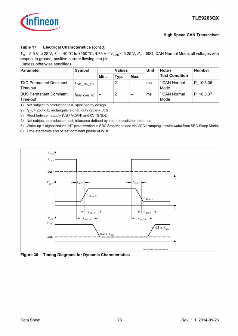
Data Sheet 73 Rev. 1.1, 2014-09-26
TLE9263QX
High Speed CAN Transceiver
Figure 30 Timing Diagrams for Dynamic Characteristics
TXD Permanent Dominant Time-out
tTxD_CAN_TO – 2 – ms 4)CAN Normal Mode
P_10.3.36
BUS Permanent Dominant Time-out
tBUS_CAN_TO – 2 – ms 4)CAN Normal Mode
P_10.3.37
1) Not subject to production test, specified by design.2) fTXD = 250 kHz rectangular signal, duty cycle = 50%;3) Rtest between supply (VS / VCAN) and 0V (GND);4) Not subject to production test, tolerance defined by internal oscillator tolerance;5) Wake-up is signalized via INT pin activation in SBC Stop Mode and via VCC1 ramping up with wake from SBC Sleep Mode;6) Time starts with end of last dominant phase of WUP;
Table 17 Electrical Characteristics (cont’d)VS = 5.5 V to 28 V; Tj = -40 °C to +150 °C; 4.75 V < VCAN < 5.25 V; RL = 60Ω; CAN Normal Mode; all voltages withrespect to ground, positive current flowing into pin (unless otherwise specified)Parameter Symbol Values Unit Note /
Test ConditionNumber
Min. Typ. Max.
t d(L),R
t
VDIFF
td(L),TR
t d(H),R
td(H),TR
td(L),Tt
GND
VTXD
V CC1
td(H),T
V diff, rd_NV diff, dr_N
t
GND0.2 x VCC1
0.8 x VCC1
V RXD
VCC1
CAN dynamic characteristics.vsd

Data Sheet 74 Rev. 1.1, 2014-09-26
TLE9263QX
High Speed CAN Transceiver
Figure 31 Timing Diagrams for RXD recessive bit width definition tbit(RXD)

Data Sheet 75 Rev. 1.1, 2014-09-26
TLE9263QX
LIN Transceiver
11 LIN Transceiver
11.1 Block Description
Figure 32 Block Diagram
11.1.1 LIN SpecificationsThe LIN network is standardized by international regulations. The device is compliant to the specification LIN 2.2.The physical layer specification LIN 2.2 is a super set of the previous LIN specifications, like LIN 2.0 or LIN 1.3.The integrated LIN transceivers are according to the LIN 2.2 standard. The device is compliant to the physical layer standard SAE-J2602-2. The SAE-J2602-2 standard differs from theLIN 2.2 standard mainly by the lower data rate (10.4 kbit/s).
Driver
Temp.-Protection
CurrentLimit
OutputStage
TxD Input
Receiver
RXDLIN
LIN
TXDLIN
VSHS
RBUS
Filter
Timeout
RTxD
VCC1
To SPI Diagnostic
SPI Mode Control
VCC1
WakeReceiver
VSHS
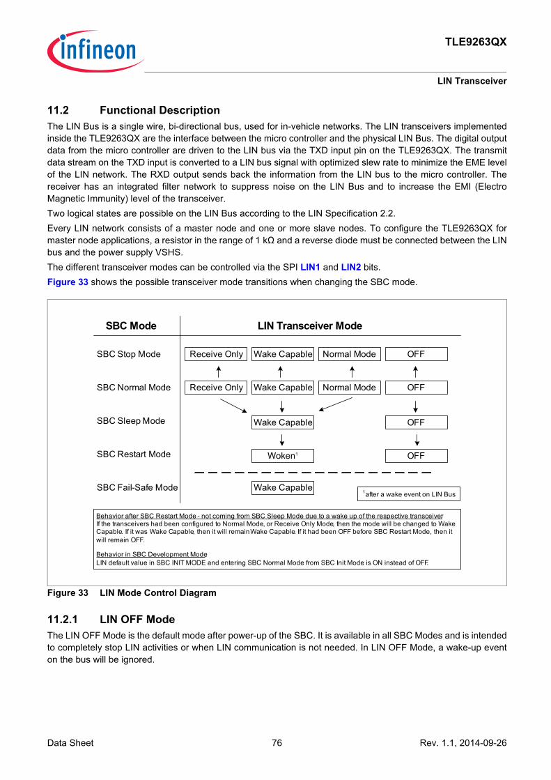
Data Sheet 76 Rev. 1.1, 2014-09-26
TLE9263QX
LIN Transceiver
11.2 Functional DescriptionThe LIN Bus is a single wire, bi-directional bus, used for in-vehicle networks. The LIN transceivers implementedinside the TLE9263QX are the interface between the micro controller and the physical LIN Bus. The digital outputdata from the micro controller are driven to the LIN bus via the TXD input pin on the TLE9263QX. The transmitdata stream on the TXD input is converted to a LIN bus signal with optimized slew rate to minimize the EME levelof the LIN network. The RXD output sends back the information from the LIN bus to the micro controller. Thereceiver has an integrated filter network to suppress noise on the LIN Bus and to increase the EMI (ElectroMagnetic Immunity) level of the transceiver. Two logical states are possible on the LIN Bus according to the LIN Specification 2.2.Every LIN network consists of a master node and one or more slave nodes. To configure the TLE9263QX formaster node applications, a resistor in the range of 1 kΩ and a reverse diode must be connected between the LINbus and the power supply VSHS.The different transceiver modes can be controlled via the SPI LIN1 and LIN2 bits.Figure 33 shows the possible transceiver mode transitions when changing the SBC mode.
Figure 33 LIN Mode Control Diagram
11.2.1 LIN OFF ModeThe LIN OFF Mode is the default mode after power-up of the SBC. It is available in all SBC Modes and is intendedto completely stop LIN activities or when LIN communication is not needed. In LIN OFF Mode, a wake-up eventon the bus will be ignored.
SBC Normal Mode
SBC Mode LIN Transceiver Mode
SBC Stop Mode
SBC Sleep Mode
SBC Restart Mode
Receive Only Normal Mode OFFWake Capable
Receive Only OFFWake Capable
OFFWoken1
OFFWake Capable
Normal Mode
Behavior after SBC Restart Mode - not coming from SBC Sleep Mode due to a wake up of the respective transceiver: If the transceivers had been configured to Normal Mode, or Receive Only Mode, then the mode will be changed to Wake Capable. If it was Wake Capable, then it will remain Wake Capable. If it had been OFF before SBC Restart Mode, then it will remain OFF.
Behavior in SBC Development Mode: LIN default value in SBC INIT MODE and entering SBC Normal Mode from SBC Init Mode is ON instead of OFF.
1after a wake event on LIN BusSBC Fail-Safe Mode Wake Capable

Data Sheet 77 Rev. 1.1, 2014-09-26
TLE9263QX
LIN Transceiver
11.2.2 LIN Normal ModeThe LIN Transceiver is enabled via SPI in SBC Normal Mode. LIN Normal Mode is designed for normal datatransmission/reception within the LIN network. The Mode is available in SBC Normal Mode and in SBC Stop Mode.
TransmissionThe signal from the microcontroller is applied to the TXDLIN input of the SBC. The bus driver switches the LIN output stage to transfer this input signal to the LIN bus line.
Enabling SequenceThe LIN transceiver requires an enabling time tLIN,EN before a message can be sent on the bus. This means thatthe TXDLIN signal can only be pulled LOW after the enabling time. If this is not ensured, then the TXDLIN needsto be set back to high (=recessive) until the enabling time is completed. Only the next dominant bit will be transmitted on the bus. Figure 34 shows different scenarios and explanations for LIN enabling.
Figure 34 LIN Transceiver Enabling Sequence
Reduced Electromagnetic Emission To reduce electromagnetic emissions (EME), the bus driver controls LIN slopes symmetrically. The configurationof the different slopes is described in Chapter 11.2.8.
ReceptionAnalog LIN bus signals are converted into digital signals at RXD via the differential input receiver.
11.2.3 LIN Receive Only ModeIn LIN Receive Only Mode (RXD only), the driver stage is de-activated but reception is still possible. This mode isaccessible by an SPI command and is available in SBC Normal and SBC Stop Mode.
t
VLIN_BUS
t LIN,ENt
VTXDLIN
t
LIN Mode
LIN NORMAL
LIN OFF
LIN,ENt LIN,ENt
recessive TXD level required bevor start of
transmission
tLIN, EN not ensured , no transmission on bus
Correct sequence , Bus is enabled after tLIN, EN
tLIN, EN not ensured , no transmission on bus
recessive TXDlevel required
Recessive
Dominant

Data Sheet 78 Rev. 1.1, 2014-09-26
TLE9263QX
LIN Transceiver
11.2.4 LIN Wake Capable ModeThis mode can be used in SBC Stop, Sleep, Restart and Normal Mode by programming via SPI and it is used tomonitor bus activities. It is automatically accessed in SBC Fail-Safe Mode. A wake-up signal on the bus (filter timet > tWK,Bus) results in different behavior of the SBC, as described in below Table 18. As a signalization to themicrocontroller, the RXD_LIN pin is set LOW and will stay LOW until the LIN transceiver is changed to any othermode. After a wake-up event the transceiver can be switched to LIN Normal Mode for communication.
Rearming the transceiver for wake capabilityAfter a BUS wake-up event, the transceiver is woken. However, the LIN1 and LIN2 transceiver mode bits will stillshow wake capable (=‘01’) so that the RXD signal will be pulled low. There are two possibilities how the LINtransceiver’s wake capable mode is enabled again after a wake event:• The LIN transceiver mode must be toggled, i.e. switched to LIN Normal Mode, LIN Receive Only Mode or LIN
Off, before switching to LIN Wake Capable Mode again.• Rearming is done automatically when the SBC is changed to SBC Stop, SBC Sleep, or SBC Fail-Safe Mode
to ensure wake-up capability.
Wake-Up in SBC Stop and SBC Normal ModeIn SBC Stop Mode, if a wake-up is detected, it is signaled by the INT output and in the WK_STAT_1 SPI register.It is also signaled by RXDLIN put to LOW. The same applies for the SBC Normal Mode. The microcontroller shouldset the device to SBC Normal Mode, there is no automatic transition to Normal Mode. For functional safety reasons, the watchdog will be automatically enabled in SBC Stop Mode after a Bus wakeevent in case it was disabled before (if bit WD_EN_ WK_BUS was configured to HIGH before).
Wake-Up in SBC Sleep ModeWake-up is possible via a LIN message (filter time t > tWK,Bus). The wake-up automatically transfers the SBC intothe SBC Restart Mode and from there to Normal Mode the corresponding RXD pin in set to LOW. Themicrocontroller is able to detect the low signal on RXD and to read the wake source out of the WK_STAT_1register via SPI. No interrupt is generated when coming out of Sleep Mode. The microcontroller can now switchthe LIN transceiver into LIN Normal Mode via SPI to start communication.
Table 18 Action due to a LIN BUS Wake-upSBC Mode SBC Mode after Wake VCC1 INT RXDNormal Mode Normal Mode ON LOW LOWStop Mode Stop Mode ON LOW LOWSleep Mode Restart Mode Ramping Up HIGH LOWRestart Mode Restart Mode ON HIGH LOWFail-Safe Mode Restart Mode Ramping up HIGH LOW

Data Sheet 79 Rev. 1.1, 2014-09-26
TLE9263QX
LIN Transceiver
11.2.5 TXD Time-out FeatureIf the TXD signal is dominant for the time t >tTxD_LIN _TO, the TXD time-out function deactivates the LIN transmitteroutput stage temporarily. The transceiver remains in recessive state. The TXD time-out functions prevents the LINbus from being blocked by a permanent LOW signal on the TXD pin, caused by a failure. The failure is stored inthe SPI flag LIN1_FAIL and LIN2_FAIL. The LIN transmitter stage is activated again after the dominant time-outcondition is removed. The transceiver configuration stays unchanged.
Figure 35 TXD Time-Out Function
11.2.6 Bus Dominant ClampingIf the LIN bus signal is dominant for a time t > tBUS_LIN_TO regardless of the LIN transceiver mode, a bus dominantclamping is detected and the SPI bit LIN1_FAIL and LIN2_FAIL is set. The transceiver configuration staysunchanged.
11.2.7 Under-Voltage DetectionIn case the supply voltage is dropping below the VSHS under-voltage detection threshold (VSHS < VSHS,UVD), theTLE9263QX disables the output and receiver stages. If the power supply reaches a higher level than the undervoltage detection threshold (VSHS > VSHS,UVD), the TLE9263QX continues with normal operation. The transceiverconfiguration stays unchanged.
TxD
LIN
ttorecttimeoutNormal Communication
Normal Communication
TxD Time-Out due to microcontroller error
Release after TxD Time-out
Recovery of the microcontroller error
t
t

Data Sheet 80 Rev. 1.1, 2014-09-26
TLE9263QX
LIN Transceiver
11.2.8 Slope SelectionThe LIN transceiver offers a LIN Low-Slope Mode for 10.4 kBaud communication and a LIN Normal-Slope Modefor 20 kBaud communication. The only difference is the behavior of the transmitter. In LIN Low-Slope Mode, thetransmitter uses a lower slew rate to further reduce the EME compared to Normal-Slope Mode. This complies withSAE J2602 requirements.By default, the device works in LIN Normal-Slope Mode. The selection of LIN Low-SlopeMode is done by an SPI bit LIN_LSM and will become effective as soon as CSN goes ‘HIGH’. Only the LIN Slopeis changed. The selection is accessible in SBC Normal Mode only.
11.2.9 Flash Programming via LINThe device allows LIN flash programming, e.g. of another LIN Slave with a communication of up to 115 kBaud.This feature is enabled by de-activating the slope control mechanism via a SPI command (bit LIN_FLASH) andwill become effective as soon as CSN goes ‘HIGH’. The SPI bit can be set in SBC Normal Mode.Note: It is recommended to perform flash programming only at nominal supply voltage VSHS = 13.5V to ensure
stable data communication.

Data Sheet 81 Rev. 1.1, 2014-09-26
TLE9263QX
LIN Transceiver
11.3 Electrical Characteristics
Table 19 Electrical CharacteristicsVSHS = 5.5 V to 18 V, Tj = -40 °C to +150 °C, RL = 500 Ω, all voltages with respect to ground, positive currentflowing into pin (unless otherwise specified)Parameter Symbol Values Unit Note / Test Condition Number
Min. Typ. Max.Receiver Output (RXD pin)HIGH Level Output Voltage VRXD,H 0.8 ×
VCC1
– – V IRXD = -1.6 mA;VBus = VSHS
P_11.3.1
LOW Level Output Voltage VRXD,L – – 0.2 × VCC1
V IRXD = 1.6 mAVBus = 0 V
P_11.3.2
Transmission Input (TXD pin)HIGH Level Input Voltage VTXD,H 0.7 ×
VCC1
– – V Recessive State P_11.3.3
TXD Input Hysteresis VTXD,hys – 0.12 × VCC1
– mV 1) P_11.3.4
LOW Level Input Voltage VTXD,L – – 0.3 × VCC1
V Dominant State P_11.3.5
TXD Pull-up Resistance RTXD 20 40 80 kΩ VTXD = 0 V P_11.3.6LIN Bus Receiver (LIN Pin)Receiver Threshold Voltage, Recessive to Dominant Edge
VBus,rd 0.4 × VSHS
0.45 × VSHS
– V P_11.3.7
Receiver Dominant State VBus,dom – – 0.4 × VSHS
V LIN 2.2 Param. 17 P_11.3.8
Receiver Threshold Voltage, Dominant to Recessive Edge
VBus,dr – 0.55 × VSHS
0.60 × VSHS
V P_11.3.9
Receiver Recessive State VBus,rec 0.6 × VSHS
– – V LIN 2.2 Param 18 P_11.3.10
Receiver Center Voltage VBus,c 0.475 × VSHS
0.5 × VSHS
0.525 × VSHS
V LIN 2.2 Param 19 6 V < VSHS < 18 V
P_11.3.11
Receiver Hysteresis VBus,hys 0.07 × VSHS
0.1 × VSHS
0.175 × VSHS
V Vbus,hys = Vbus,dr - Vbus,rdLIN 2.2 Param 20
P_11.3.12
Wake-up Threshold Voltage VBus,wk 0.40 × VSHS
0.5 × VSHS
0.6 × VSHS
V – P_11.3.13
Dominant Time for Bus Wake-up
tWK,Bus 30 – 150 µs 2) P_11.3.14

Data Sheet 82 Rev. 1.1, 2014-09-26
TLE9263QX
LIN Transceiver
LIN Bus Transmitter (LIN Pin)Bus Serial Diode Voltage Drop Vserdiode 0.4 0.7 1.0 V 1) VTXD = VCC1;
LIN 2.2 Param 21P_11.3.15
Bus Recessive Output Voltage
VBUS,ro 0.8 × VSHS
– VSHS V VTXD = HIGH Level P_11.3.16
Bus Short Circuit Current IBUS,sc 40 100 150 mA VBUS = 18 V;LIN 2.2 Param 12
P_11.3.17
Leakage CurrentLoss of Ground
IBUS,lk1 -1000 -450 20 µA VSHS = 12 V = GND;0 V < VBUS < 18 V;LIN 2.2 Param 15
P_11.3.18
Leakage CurrentLoss of Battery
IBUS,lk2 – – 20 µA VSHS = 0 V;VBUS = 18 V;LIN 2.2 Param 16
P_11.3.19
Leakage CurrentDriver Off
IBUS,lk3 -1 – – mA VSHS = 18 V;VBUS = 0 V;LIN 2.2 Param 13
P_11.3.20
Leakage CurrentDriver Off
IBUS,lk4 – – 20 µA VSHS = 8 V;VBUS = 18 V;LIN 2.2 Param 14
P_11.3.21
Bus Pull-up Resistance RBUS 20 30 47 kΩ Normal ModeLIN 2.2 Param 26
P_11.3.22
LIN Input Capacitance CBUS 20 25 pF 1) P_11.3.23Receiver propagation delaybus dominant to RXD LOW
td(L),R – 1 6 µs VCC = 5 V;CRXD = 20 pF;LIN 2.2 Param 31
P_11.3.24
Receiver propagation delaybus recessive to RXD HIGH
td(H),R – 1 6 µs VCC = 5 V;CRXD = 20 pF;LIN 2.2 Param 31
P_11.3.25
Receiver delay symmetry tsym,R -2 – 2 µs tsym,R = td(L),R - td(H),R;LIN 2.2 Param 32
P_11.3.26
LIN Transceiver Enabling Time
tLIN,EN – 10 – µs 2) CSN = HIGH to first valid transmitted TXD dominant
P_11.3.27
Bus Dominant Time Out tBUS_LIN
_TO
– 20 – ms 1)2) P_11.3.28
TXD Dominant Time Out tTxD_LIN
_TO
– 20 – ms 1)2)VTXD = 0 V P_11.3.29
TXD Dominant Time Out Recovery Time
ttorec – 10 – µs 1)2) P_11.3.30
Table 19 Electrical Characteristics (cont’d)VSHS = 5.5 V to 18 V, Tj = -40 °C to +150 °C, RL = 500 Ω, all voltages with respect to ground, positive currentflowing into pin (unless otherwise specified)Parameter Symbol Values Unit Note / Test Condition Number
Min. Typ. Max.

Data Sheet 83 Rev. 1.1, 2014-09-26
TLE9263QX
LIN Transceiver
Duty Cycle D1(For worst case at 20 kbit/s)LIN 2.2 Normal Slope
D1 0.396 – – 3) THRec(max) = 0.744 × VSHS;THDom(max) = 0.581 × VSHS;VSHS = 7.0 … 18 V;tbit = 50 µs;D1 = tbus_rec(min)/2 tbit;LIN 2.2 Param 27
P_11.3.31
Duty Cycle D2(for worst case at 20 kbit/s)LIN 2.2 Normal Slope
D2 – – 0.581 3)THRec(min.) = 0.422 × VSHS;THDom(min.) = 0.284 × VSHS;VSHS = 7.6 … 18 V;tbit = 50 µs;D2 = tbus_rec(max)/2 tbit;LIN 2.2 Param 28
P_11.3.32
Duty Cycle D3(for worst case at 10.4 kbit/s)SAE J2602 Low Slope
D3 0.417 – – 3)THRec(max) = 0.778 × VSHSTHDom(max) = 0.616 × VSHS;VSHS = 7.0 … 18 V;tbit = 96 µs;D3 = tbus_rec(min)/2 tbit;LIN 2.2 Param 29
P_11.3.33
Duty Cycle D4(for worst case at 10.4 kbit/s)SAE J2602 Low Slope
D4 – – 0.590 3)THRec(min.) = 0.389 × VSHS;THDom(min.) = 0.251 × VSHS;VSHS = 7.6 … 18 V;tbit = 96 µs;D4 = tbus_rec(max)/2 tbit;LIN 2.2 Param 30
P_11.3.34
1) Not subject to production test, specified by design.2) Not subject to production test, tolerance defined by internal oscillator tolerance3) Bus load conditions concerning LIN Specification 2.2 CLIN, RLIN = 1 nF, 1 kΩ / 6.8 nF, 660 Ω/ 10 nF, 500 Ω
Table 19 Electrical Characteristics (cont’d)VSHS = 5.5 V to 18 V, Tj = -40 °C to +150 °C, RL = 500 Ω, all voltages with respect to ground, positive currentflowing into pin (unless otherwise specified)Parameter Symbol Values Unit Note / Test Condition Number
Min. Typ. Max.

Data Sheet 84 Rev. 1.1, 2014-09-26
TLE9263QX
LIN Transceiver
Figure 36 Simplified Test Circuit for Dynamic Characteristics
GNDLIN
100 nF
VSHS
CLIN
TxD
WK
RLINRxD
CRxD

Data Sheet 85 Rev. 1.1, 2014-09-26
TLE9263QX
LIN Transceiver
Figure 37 Timing Diagram for Dynamic Characteristics
tBit tBit tBit
tBus _dom (max ) tBus_rec (min )
Thresholds of receiving node 1
Thresholds of receiving node 2
THRec (max)
THDom (max)
THRec(min)
THDom(min )
tBus _dom (min ) tBus_rec(max )
td(L),R(1) td (H),R(1 )
td (H),r(2)t(L),R(2)
VSUP(Transceiver supply of transmitting node )
TxD(input to transmitting node )
RxD(output of receiving node 1)
RxD(output of receiving node 2)
Duty Cycle 1 = tBUS_rec(min) / (2 x tBIT)
Duty Cycle 2 = tBUS_rec(max ) / (2 x tBIT)

Data Sheet 86 Rev. 1.1, 2014-09-26
TLE9263QX
Wake and Voltage Monitoring Inputs
12 Wake and Voltage Monitoring Inputs
12.1 Block Description
Figure 38 Wake Input Block Diagram
Features• Three High-Voltage inputs with a 3V (typ.) threshold voltage• Alternate Measurement function for high-voltage sensing via WK1 and WK2• Wake-up capability for power saving modes• Edge sensitive wake feature LOW to HIGH and HIGH to LOW• Pull-up and Pull-down current sources, configurable via SPI• Selectable configuration for static sense or cyclic sense working with TIMER1, TIMER2• In SBC Normal and SBC Stop Mode the level of the WK pin can be read via SPI even if the respective WK is
not enabled as a wake source.
MONx_Input_Circuit_ext.vsd
+
-tWK
WKx
Internal Supply
Logic
IPD_WK
IPU_WK
VRef

Data Sheet 87 Rev. 1.1, 2014-09-26
TLE9263QX
Wake and Voltage Monitoring Inputs
12.2 Functional DescriptionThe wake input pins are edge-sensitive inputs with a switching threshold of typically 3V. This means that bothtransitions, HIGH to LOW and LOW to HIGH, result in a signalization by the SBC. The signalization occurs eitherin triggering the interrupt in SBC Normal Mode and SBC Stop Mode or by a wake up of the device in SBC Sleepand SBC Fail-Safe Mode.
Two different wake detection modes can be selected via SPI: • Static sense: WK inputs are always active• Cyclic sense: WK inputs are only active for a certain time period (see Chapter 5.2.1)
Two different filter times of 16µs or 64µs can be selected to avoid a parasitic wake-up due to transients or EMCdisturbances in static sense configuration.The filter time (tFWK1, tFWK2) is triggered by a level change crossing the switching threshold and a wake signal isrecognized if the input level will not cross again the threshold during the selected filter time.Figure 39 shows a typical wake-up timing and parasitic filter.
Figure 39 Wake-up Filter Timing for Static Sense
The wake-up capability for each WK pin can be enabled or disabled via SPI command in the WK_CTRL_2register. The wake source for a wake via a WKx pin can always be read in the register WK_STAT_1 at the bits WK1_WU,WK2_WU, and WK3_WU.The actual voltage level of the WK pin (LOW or HIGH) can always be read in SBC Normal and SBC Stop Modein the register WK_LVL_STAT. During Cyclic Sense, the register show the sampled levels of the respective WKpin.
If FO2...3 are configured as WK inputs in its alternative function (16µs static filter time), then the wake events willbe signalled in the register WK_STAT_2.
VWK,th
t
VWK
tWK,f
No Wake Event Wake Event
VWK,th
tWK,f
t
VINT
tINT

Data Sheet 88 Rev. 1.1, 2014-09-26
TLE9263QX
Wake and Voltage Monitoring Inputs
12.2.1 Wake Input ConfigurationTo ensure a defined and stable voltage levels at the internal comparator input it is possible to configure integratedcurrent sources via the SPI register WK_PUPD_CTRL. In addition, the wake detection modes (including the filtertime) can be configured via the SPI register WK_FLT_CTRL. An example illustration for the automatic switchingconfiguration is shown in Figure 40.
Note: If there is no pull-up or pull-down configured on the WK input, then the respective input should be tied to GND or VS on board to avoid unintended floating of the pin and subsequent wake events.
Figure 40 Illustration for Pull-Up / Down Current Sources with Automatic Switching Configuration
Config A and B are intended for static sense with two different filter times. Config C or D are intended for cyclic sense configuration. With the filter settings, the respective timer needs to beassigned to one or more HS output, which supplies an external circuit connected to the WKx pin, e.g. HS1controlled by Timer 2 (HS1 = 010) and connected to WK3 via an switch circuitry - see also Chapter 5.2.
Table 20 Pull-Up / Pull-Down ResistorWKx_PUPD_1
WKx_PUPD_0
Current Sources Note
0 0 no current source WKx input is floating if left open (default setting)0 1 pull-down WKx input internally pulled to GND1 0 pull-up WKx input internally pulled to internal 5V supply1 1 Automatic
switchingIf a high level is detected at the WKx input the pull-up source is activated, if low level is detected the pull down is activated.
Table 21 Wake Detection Configuration and Filter TimeWKx_FLT_1 WKx_FLT_0 Filter Time Description0 0 Config A static sense, 16µs filter time0 1 Config B static sense, 64µs filter time1 0 Config C Cyclic sense, Timer 1, 16µs filter time. Period, On-time
configurable in register TIMER1_CTRL1 1 Config D Cyclic sense, Timer 2, 16µs filter time. Period, On-time
configurable in register TIMER2_CTRL
IWK
IWKth_min IWKth_max
VWKth
Data Sheet 89 Rev. 1.1, 2014-09-26
TLE9263QX
Wake and Voltage Monitoring Inputs
12.2.2 Alternate Measurement Function with WK1 and WK2
12.2.2.1 Block DescriptionThis function provides the possibility to measure a voltage, e.g. the unbuffered battery voltage, with the protectedWK1 HV-input. The measured voltage is routed out at WK2. It allows for example a voltage compensation for LEDlighting by changing the duty cycle of the High-Side outputs. A simple voltage divider needs to be placed externallyto provide the correct voltage level to the microcontroller A/D converter input. The function is available in SBC Normal Mode and it is disabled in all other modes to allow a low-quiescent currentoperation.The measurement function can be used instead of the WK1 and WK2 wake and level signallingcapability. The benefits of the function is that the signal is measured by a HV-input pin and that there is no current flowingthrough the resistor divider during low-power modes.The functionality is shown in a simplified application diagram in Figure 61.
12.2.2.2 Functional DescriptionThis measurement function is by default disabled. In this case, WK1 and WK2 have the regular wake and voltagelevel signalization functionality. The switch S1 is open for this configuration (see Figure 61).The measurement function can be enabled via the SPI bit WK_MEAS.If WK_MEAS is set to ‘1’, then the measurement function is enabled and switch S1 is closed in SBC Normal Mode.S1 is open in all other SBC modes. If this function the pull-up and down currents of WK1 and WK2 are disabled,and the internal WK1 and WK2 signals are gated. In addition, the settings for WK1 and WK2 in the registersWK_PUPD_CTRL, WK_FLT_CTRL and WK_CTRL_2 are ignored but changing these setting is not prevented.The registers WK_STAT_1 and WK_LVL_STAT are not updated with respect to the inputs WK1 and WK2. However, if only WK1 or WK2 are set as wake sources and a SBC Sleep Mode command is set, then the SPI_FAILflag will be set and the SBC will be changed into SBC Restart Mode (see Chapter 5.1 also for wake capability ofWK1 and WK2).
Note: There is a diode in series to the switch S1 (not shown in the Figure 61), which will influence the temperature behavior of the switch.
Table 22 Differences between Normal WK Function and Measurement FunctionAffected Settings/Modules for WK1 and WK2 Inputs
WK_MEAS = 0 WK_MEAS = 1
S1 configuration ‘open’ ‘closed’ in SBC Normal Mode, ‘open’ in all other SBC Modes
Internal WK1 & WK2 signal processing
Default wake and level signaling function, WK_STAT_1, WK_STAT_2 are updated accordingly
‘WK1...2 inputs are gated internally, WK_STAT_1, WK_STAT_2 are not updated
WK1_EN, WK2_EN Wake-up via WK1 and WK2 possible if bits are set
setting the bits is ignored and not prevented. If only WK1_EN, WK2_EN are set while trying to go to SBC Sleep Mode, then the SPI_FAIL flag will be set and the SBC will be changed into SBC Restart Mode.
WK_PUPD_CTRL normal configuration is possible no pull-up or pull-down enabledWK_FLT_CTRL normal configuration is possible setting the bits is ignored and not
prevented

Data Sheet 90 Rev. 1.1, 2014-09-26
TLE9263QX
Wake and Voltage Monitoring Inputs
12.3 Electrical Characteristics
Table 23 Electrical CharacteristicsVS = 5.5 V to 28 V; Tj = -40 °C to +150 °C; all voltages with respect to ground, positive current flowing into pin (unless otherwise specified)Parameter Symbol Values Unit Note / Test Condition Number
Min. Typ. Max.WK1...WK3 Input Pin CharacteristicsWake-up/monitoring threshold voltage
VWKth 2 3 4 V without external serial resistor RS (with RS: ∆V = IPD/PU * RS);hysteresis included
P_12.3.1
Threshold hysteresis VWKNth,hys 0.1 - 0.7 V without external serial resistor RS (with RS: ∆V = IPD/PU * RS);
P_12.3.2
WK pin Pull-up Current IPU_WK -20 -10 -3 µA VWK_IN = 4V P_12.3.3WK pin Pull-down Current
IPD_WK 3 10 20 µA VWK_IN = 2V P_12.3.4
Input leakage current ILK,l -2 2 µA 0 V < VWK_IN < 40V P_12.3.5Drop Voltage across S1 switch
VDrop,S1 – 1000 – mV 1)Drop Voltage between WK1 and WK2 when enabled for voltage measurement; IWK1 = 500µA; Tj = 25°CRefer to Figure 41
1) Not subject to production test; specified by design
P_12.3.13
TimingWake-up filter time 1 tFWK1 - 16 - µs 2)SPI Setting
2) Not subject to production test, tolerance defined by internal oscillator tolerance
P_12.3.6Wake-up filter time 2 tFWK2 - 64 - µs 2)SPI Setting P_12.3.7

Data Sheet 91 Rev. 1.1, 2014-09-26
TLE9263QX
Wake and Voltage Monitoring Inputs
Figure 41 Typical Drop Voltage Characteristics of S1 (between WK1 & WK2)
800
900
1000
1100
AGEDR
OPOFSW
ITCH
S1(m
V)
VS = 13.5V
250 μA
500 μA
500
600
700
50 0 50 100 150
V S1,VO
LTA
Tj JUNCTIONTEMPERATURE(°C)
50 μA
100 μA

Data Sheet 92 Rev. 1.1, 2014-09-26
TLE9263QX
Interrupt Function
13 Interrupt Function
13.1 Block and Functional Description
Figure 42 Interrupt Block Diagram
The interrupt is used to signalize special events in real time to the microcontroller. The interrupt block is designedas a push/pull output stage as shown in Figure 42. An interrupt is triggered and the INT pin is pulled low (activelow) for tINT in SBC Normal and Stop Mode and it is released again once tINT is expired. The minimum HIGH-timeof INT between two consecutive interrupts is tINTD. An interrupt does not cause a SBC mode change.Two different interrupt classes could be selected via the SPI bit INT_ GLOBAL:• Class 1 (wake interrupt - INT_ GLOBAL=0): all wake-up events stored in the wake status SPI register
(WK_STAT_1 and WK_STAT_2) cause an interrupt (default setting). An interrupt is only triggered if the respective function is also enabled as a wake source (including GPIOx if configured as a wake input).
• Class 2 (global interrupt - INT_ GLOBAL=1): in addition to the wake-up events, all signalled failures stored in the other status registers cause an interrupt (the register WK_LVL_STAT is not generating interrupts)
Note: The errors which will cause SBC Restart or SBC Fail-Safe Mode (Vcc1_UV, WD_FAIL, VCC1_SC, TSD2, FAILURE) are the exceptions of an INT generation on status bits. Also POR and DEV_STAT_x and will not generate interrupts.
In addition to this behavior, an INT will be triggered when the SBC is sent to SBC Stop Mode and not all bits werecleared in the WK_STAT_1 and WK_STAT_2register.The SPI status registers are updated at every falling edge of the INT pulse. All interrupt events are stored in therespective register (except the register WK_LVL_STAT) until the register is read and cleared via SPI command.A second SPI read after reading out the respective status register is optional but recommended to verify that theinterrupt event is not present anymore. The interrupt behavior is shown in Figure 43 for class 1 interrupts. Thebehavior for class 2 is identical. The INT pin is also used during SBC Init Mode to select the hardware configuration of the device. SeeChapter 5.1.1 for further information.
Interrupt logic
INTTime out
Vcc1

Data Sheet 93 Rev. 1.1, 2014-09-26
TLE9263QX
Interrupt Function
Figure 43 Interrupt Signalization Behavior
Interrupt_Behavior .vsd
INT
WK1 WK2
tINT
tINTD
Update of WK_STAT register
SPI Read & Clear
Update of WK_STAT register
WK_STATcontentsSc
enar
io 1
WK1 no WK WK2 no WK
optional
SPI Read & Clear
WK_STATcontentsSc
enar
io 2
WK1 + WK2 no WK
No SPI Read & Clear Command sent

Data Sheet 94 Rev. 1.1, 2014-09-26
TLE9263QX
Interrupt Function
13.2 Electrical Characteristics
Table 24 Interrupt OutputVS = 5.5 V to 28 V; Tj = -40 °C to +150 °C; SBC Normal Mode; all voltages with respect to ground; positive currentdefined flowing into pin; unless otherwise specified.Parameter Symbol Values Unit Note /
Test ConditionNumber
Min. Typ. Max.Interrupt Output; Pin INTINT High Output Voltage VINT,H 0.8 ×
VCC1
– – V 1)IINT = -1 mA;INT = OFF
1) Output Voltage Value also determines device configuration during SBC Init Mode
P_13.2.1
INT Low Output Voltage VINT,L – – 0.2 × VCC1
V 1)IINT = 1 mA;INT = ON
P_13.2.2
INT Pulse Width tINT – 100 – µs 2)
2) Not subject to production test, tolerance defined by internal oscillator tolerance.
P_13.2.3INT Pulse Minimum Delay Time
tINTD – 100 – µs 2) between consecutive pulses
P_13.2.4
Configuration Select; Pin INTConfig Pull-down Resistance
RCFG – 250 – kΩ VINT = 5 V P_13.2.5
Config Select Filter Time tCFG_F – 7 – µs 2) P_13.2.6

Data Sheet 95 Rev. 1.1, 2014-09-26
TLE9263QX
Fail Outputs
14 Fail Outputs
14.1 Block and Functional Description
Figure 44 Simplified Fail Output Block Diagram for FO1/2 and for FO3/TEST
The fail outputs consist of a failure logic block and three open-drain outputs (FO1, FO2, FO3) with active-lowsignalization.The fail outputs are activated due to following failure conditions:• Watchdog trigger failure (For config 3&4 only after the 2nd watchdog trigger failure and for config 1&2 after 1st
watchdog trigger failure)• Thermal shutdown TSD2• VCC1 short to GND• VCC1 over voltage (only if the SPI bit VCC1_OV_RST is set)• After 4 consecutive VCC1 under voltage event (see Chapter 15.6 for details)At the same time SBC Fail-Safe Mode is entered (exceptions are watchdog trigger failures depending on selected configurations - see Chapter 5.1.1).The fail output activation is signalled in the SPI bit FAILURE of the register DEV_STAT. For testing purposes only the Fail Outputs can also be activated via SPI by setting the bit FO_ON. This bit isindependent of the FO failure bits. In case that there is no failure condition, the FO outputs can also be turned offagain via SPI, i.e. no successful watchdog trigger is needed.The entry of SBC Fail-Safe Mode due to a watchdog failure can be configured as described in Chapter 5.1.1.In order to deactivate the fail outputs in SBC Normal Mode the failure conditions must not be present anymore(e.g. TSD2, VCC1 short circuit, etc) and the bit FAILURE needs to be cleared via SPI command. In case of aFAILURE bit setting due to a watchdog fail, a successful WD trigger is needed in addition, i.e. WD_FAIL must becleared. WD_FAIL will also be cleared when going to SBC Sleep or SBC Fail-Safe Mode due to another failure(not a WD failure) or if the watchdog is disabled in SBC Stop Mode.Note: The Fail output pin is triggered for any of the above described failures. No FAILURE is caused for the 1st
watchdog failure if selected for Config2.
The three fail outputs are activated simultaneously with following output functionalities: • FO1: Static fail output• FO2: 1.25Hz, 50% (typ.) duty cycle, e.g. to generate an indicator signal
Failure logic
FO1/2
FO3/TEST
5V_int
RTEST
SBC Init Mode
Failure Logic
T test
T FO_PL

Data Sheet 96 Rev. 1.1, 2014-09-26
TLE9263QX
Fail Outputs
• FO3: 100Hz PWM, 20% (typ.) duty cycle, e.g. to generate a dimmed rear light from a break light.Note: The duty cycle for FO3 can be configured via SPI option to 20%, 10%, 5% or 2.5%. Default value is 20%.
See the register FO_DC for configuration.
14.1.1 General Purpose I/O Functionality of FO2 and FO3 as Alternate Function In case that FO2 and FO3 are not used in the application, those pins can also be configured with an alternatefunction as high-voltage (VSHS related) General Purpose I/O pins.
Figure 45 Simplified General Purpose I/O block diagram for FO2 and FO3/TEST
The pins are by default configured as FO pins. The configuration is done via the SPI register GPIO_CTRL. Thealternate function can be:• Wake Inputs: The detection threshold VGPIOI,th is similar as for the WK inputs. The wake-up detection behavior
is the same as for WKx pins. Wake events are stored and reported in WK_STAT_2.• Low-Side Switches: The switch is able to drive currents of up to 10mA (see also VGPIOL,L1). It is self-protected
with regards to current limitation. No other diagnosis is implemented.• High-Side Switches: The switch is able to drive currents up to 10mA (see also VGPIOH,H1). It is self-protected
with regards to current limitation. No other diagnosis is implemented. • If configured as GPIO then the respective level at the pin will be shown in WK_LVL_STAT in SBC Normal and
Stop Mode. This is also the case if configured as LS/HS and can serve as a feedback about the respective state. GPIO2 is shared with the TEST level bit.
Figure 46 describes the behavior of the FO/GPIO pins in their different configurations and SBC modes.
Figure 46 FO / GPIO behavior for the respective SBC modes
Note: In order to avoid unintentional entry of SBC Development Mode care must be taken that the level of FO3/TEST is HIGH during device power up and SBC Init Mode.
Note: The FOx drivers are supplied via VS. However, the GPIO HS switches (FO2, FO3/TEST) are supplied by VSHS
Config & Control Logic
FOx/GPIOx
VSHS
Function Normal Mode Stop Mode Sleep Mode Fail-Safe ModeFOx keeps the state keeps the state activeWK wake capable wake capable OFFHS as configured in Normal Mode OFF OFFLS as configured in Normal Mode OFF OFF
configurable

Data Sheet 97 Rev. 1.1, 2014-09-26
TLE9263QX
Fail Outputs
14.2 Electrical Characteristics
Table 25 Interrupt OutputVSHS = 5.5 V to 28 V; Tj = -40 °C to +150 °C; SBC Normal Mode; all voltages with respect to ground; positive currentdefined flowing into pin; unless otherwise specified.1)
1) The FOx drivers are supplied via VS. However, the GPIO HS switches (FO2, FO3/TEST) are supplied by VSHS
Parameter Symbol Values Unit Note / Test Condition
NumberMin. Typ. Max.
Pin FO1FO1 low output voltage (active)
VFO,L1 – – 1.0 V IFO = 4mA P_14.2.1
FO1 high output current (inactive)
IFO,H 0 – 2 µA VFO = 28V P_14.2.2
Pin FO2FO2 side indicator frequency
fFO2SI 1.00 1.25 1.50 Hz 3) P_14.2.3
FO2 side indicator duty cycle
dFO2SI – 50 – % 3) P_14.2.4
Pin FO3/TEST2)
Pull-up Resistance at pin FO3/TEST
RTEST 2.5 5 10 kΩ VTEST =0V; SBC Init Mode
P_14.2.5
TEST Input Filter Time tTEST – 64 – µs 3) P_14.2.6FO3 pulsedlight frequency
fFO3PL 80 100 120 Hz 3) P_14.2.7
FO3 pulsed light duty cycle
dFO3PL – 20 – % 3)4)default setting P_14.2.8
Alternate FO2...3 Electrical Characteristics: GPIOGPIO low-side output voltage (active)
VGPIOL,L1 – – 1 V IGPIO = 10mA P_14.2.9
GPIO low-side output voltage (active)
VGPIOL,L2 – – 5 mV 5)IGPIO = 50µA P_14.2.17
GPIO high-side output voltage (active)
VGPIOH,H1 VSHS-1 – – V IGPO = -10mA P_14.2.10
GPIO high-side output voltage (active)
VGPIOH,H2 VSHS-5 – – mV 5)IGPO = -50µA P_14.2.18
GPIO input threshold voltage
VGPIOI,th 1.5 2.5 3.5 V 6) hysteresis included P_14.2.11
GPIO input threshold hysteresis
VGPIOI,hys 100 400 700 mV 5) P_14.2.12
GPIO low-side current limitation
IGPIOL,max 10 – 30 mA VGPIO = 28V P_14.2.13
GPIO high-side current limitation
IGPIOH,max -45 – -10 mA VGPIO = 0V P_14.2.14

Data Sheet 98 Rev. 1.1, 2014-09-26
TLE9263QX
Fail Outputs
2) The external capacitance on this pin must be limited to less than 10nF to ensure proper detection of SBC Development Mode and SBC User Mode operation.
3) Not subject to production test, tolerance defined by internal oscillator tolerance.4) The duty cyclic is adjustable via the SPI bits FO_DC.5) Not subject to production test, specified by design.6) Applies also for TEST voltage input level
Data Sheet 99 Rev. 1.1, 2014-09-26
TLE9263QX
Supervision Functions
15 Supervision Functions
15.1 Reset Function
Figure 47 Reset Block Diagram
15.1.1 Reset Output DescriptionThe reset output pin RO provides a reset information to the microcontroller, for example, in the event that theoutput voltage has fallen below the under voltage threshold VRT1/2/3/4. In case of a reset event, the reset output ROis pulled to low after the filter time tRF and stays low as long as the reset event is present plus a reset delay timetRD1. When connecting the SBC to battery voltage, the reset signal remains LOW initially. When the output voltageVcc1 has reached the reset default threshold VRT1,r, the reset output RO is released to HIGH after the reset delaytime tRD1. A reset can also occur due to a watchdog trigger failure. The reset threshold can be adjusted via SPI,the default reset threshold is VRT1,f. The RO pin has an integrated pull-up resistor. In case reset is triggered, it willbe pulled low for Vcc1 ≥ 1V and for VS ≥ VPOR,f (see also Chapter 15.3).The timings for the RO triggering regarding VCC1 under voltage and watchdog trigger is shown in Figure 48.
Reset logicIncl. filter & delay
RO
VCC1

Data Sheet 100 Rev. 1.1, 2014-09-26
TLE9263QX
Supervision Functions
Figure 48 Reset Timing Diagram
15.1.2 Soft Reset DescriptionIn SBC Normal and SBC Stop Mode, it is also possible to trigger a device internal reset via a SPI command inorder to bring the SBC into a defined state in case of failures. In this case the microcontroller must send a SPIcommand and set the MODE bits to ‘11’ in the M_S_CTRL register. As soon as this command becomes valid, theSBC is set back to SBC INIT Mode and all SPI registers are set to their default values (see SPI Chapter 16.5 andChapter 16.6).Two different soft reset configurations are possible via the SPI bit SOFT_ RESET_RO:• The reset output (RO) is triggered when the soft reset is executed (default setting, the same reset delay time
tRD1 applies)• The reset output (RO) is not triggered when the soft reset is executedNote: The device must be in SBC Normal Mode or SBC Stop Mode when sending this command.
Otherwise, the command will be ignored.
The reset threshold can be configured via SPI in SBC
Normal Mode , default is VRT1
tRD1 tLW
SBC Init
RO
SPI
t
VCCVRT1
undervoltage
tRD1
SBC Normal
t
t
tLW
t < tRF
tRF
tCW
SBC Restart SBC Normal
SPI Init
tCW tOW
WDTrigger
tCW tOW
WDTrigger
SPI Init
tLW= long open windowtCW= closed windowtOW= open window

Data Sheet 101 Rev. 1.1, 2014-09-26
TLE9263QX
Supervision Functions
15.2 Watchdog FunctionThe watchdog is used to monitor the software execution of the microcontroller and to trigger a reset if themicrocontroller stops serving the watchdog due to a lock up in the software. Two different types of watchdog functions are implemented and can be selected via the bit WD_WIN:• Time-Out Watchdog (default value)• Window WatchdogThe respective watchdog functions can be selected and programmed in SBC Normal Mode. The configurationstays unchanged in SBC Stop Mode.Please refer to Table 26 to match the SBC Modes with the respective watchdog modes.
The watchdog timing is programmed via SPI command. As soon as the watchdog is programmed, the timer startswith the new setting and the watchdog must be served. The watchdog is triggered by sending a valid SPI-writecommand to the watchdog configuration register. The trigger SPI command is executed when the Chip Selectinput (CSN) becomes HIGH.When coming from SBC Init, SBC Restart Mode or in certain cases from SBC Stop Mode, the watchdog timer isalways started with a long open window. The long open window (tLW = 200ms) allows the microcontroller to run itsinitialization sequences and then to trigger the watchdog via SPI.The watchdog timer period can be selected via the watchdog timing bit field (WD_TIMER) and is in the range of10 ms to 1000 ms. This setting is valid for both watchdog types.The following watchdog timer periods are available:• WD Setting 1: 10ms • WD Setting 2: 20ms• WD Setting 3: 50ms• WD Setting 4: 100ms• WD Setting 5: 200ms • WD Setting 6: 500ms• WD Setting 7: 1000msIn case of a watchdog reset, SBC Restart or SBC Fail-Safe Mode is entered according to the configuration andthe SPI bits WD_FAIL are set. Once the RO goes HIGH again the watchdog immediately starts with a long openwindow the SBC enters automatically SBC Normal Mode. In SBC Software Development Mode the watchdog is OFF and therefore no reset and interrupt are generated dueto a watchdog failure.
Table 26 Watchdog Functionality by SBC ModesSBC Mode Watchdog Mode RemarksINIT Mode Starts with Long Open Window Watchdog starts with Long Open Window after RO is
releasedNormal Mode WD Programmable Window Watchdog, Time-Out watchdog or switched
OFF for SBC Stop ModeStop Mode Watchdog is fixed or OFFSleep Mode OFF SBC will start with Long Open Window when entering
SBC Normal Mode.Restart Mode OFF SBC will start with Long Open Window when entering
SBC Normal Mode.

Data Sheet 102 Rev. 1.1, 2014-09-26
TLE9263QX
Supervision Functions
Depending on the configuration, the WD_FAIL bits will be set after a watchdog trigger failure as follows:• In case an incorrect WD trigger is received (triggering in the closed watchdog window or when the watchdog
counter expires without a valid trigger) then the WD_FAIL bits will be increased (showing the number of incorrect WD triggers)
• For config 2: the bits can have the maximum value of ‘01’ • For config 1, 3 and 4: the bits can have the maximum value of ‘10’
The WD_FAIL bits are cleared automatically when following conditions apply:• After a successful watchdog trigger• When the watchdog is OFF: in SBC Stop Mode after successfully disabling it, in SBC Sleep Mode, or in SBC
Fail-Safe Mode (except for a watchdog failure)
15.2.1 Time-Out WatchdogThe time-out watchdog is an easier and less secure watchdog than a window watchdog as the watchdog triggercan be done at any time within the configured watchdog timer period. A correct watchdog service immediately results in starting a new watchdog timer period. Taking the tolerances ofthe internal oscillator into account leads to the safe trigger area as defined in Figure 49.If the time-out watchdog period elapses, a watchdog reset is created by setting the reset output RO low and theSBC switches to SBC Restart or SBC Fail-Safe Mode.
Figure 49 Time-out Watchdog Definitions
open window
t / [tWD_TIMER]safe trigger area
Wd1_TimeOut_per.vsd
Watchdog Timer Period (WD_TIMER)
uncertainty
Typical timout watchdog trigger period
tWD x 1.80tWD x 1.20
tWD x 1.50

Data Sheet 103 Rev. 1.1, 2014-09-26
TLE9263QX
Supervision Functions
15.2.2 Window WatchdogCompared to the time-out watchdog the characteristic of the window watchdog is that the watchdog timer periodis divided between an closed and an open window. The watchdog must be triggered within the open window.A correct watchdog trigger results in starting the window watchdog period by a closed window followed by an openwindow. The watchdog timer period is at the same time the typical trigger time and defines the middle of the open window.Taking the oscillator tolerances into account leads to a safe trigger area of:tWD x 0.72 < safe trigger area < tWD x 1.20.The typical closed window is defined to a width of 60% of the selected window watchdog timer period. Taking thetolerances of the internal oscillator into account leads to the timings as defined in Figure 50. A correct watchdog service immediately results in starting the next closed window.Should the trigger signal meet the closed window or should the watchdog timer period elapse, then a watchdogreset is created by setting the reset output RO low and the SBC switches to SBC Restart or SBC Fail-Safe Mode.
Figure 50 Window Watchdog Definitions
15.2.3 Watchdog Setting Check Sum A check sum bit is part of the SPI commend to trigger the watchdog and to set the watchdog setting. The sum of the 8 data bits in the register WWD_CTRL needs to have even parity (see Equation (3)). This isrealized by either setting the bit CHECKSUM to 0 or 1. If the check sum is wrong, then the SPI command isignored, i.e. the watchdog is not triggered or the settings are not changed and the bit SPI_FAIL is set. The checksum is calculated by taking all 8 data bits into account. The written value of the reserved bit 3 of theWWD_CTRL register is considered (even if read as ‘0’ in the SPI output) for checksum calculation, i.e. if a 1 iswritten on the reserved bit position, then a 1 will be used in the checksum calculation.
(3)
closed window open window
t / [tWD _TIMER]safe trigger area
tWD x 0.72 tWD x 1.20
uncertainty uncertainty
tWD x 0.48 tWD x 1.80
Watchdog Timer Period (WD_TIMER)
Typ. closed window Typ. open window
tWD x 0.6
tWD x 1.0
tWD x 0.9
CHKSUM Bit15 … Bit8⊕ ⊕=
Data Sheet 104 Rev. 1.1, 2014-09-26
TLE9263QX
Supervision Functions
15.2.4 Watchdog during SBC Stop ModeThe watchdog can be disabled for SBC Stop Mode in SBC Normal Mode. For safety reasons, there is a specialsequence to be followed in order to disable the watchdog as described in Figure 51. Two different SPI bits(WD_STM_ EN_0, WD_STM_ EN_1) in the registers WK_CTRL_1 and WD_CTRL need to be set.
Figure 51 Watchdog disabling sequence in SBC Stop Mode
If a sequence error occurs, then the bit WD_STM_ EN_1 will be cleared and the sequence has to be started again.The watchdog can be enabled by triggering the watchdog in SBC Stop Mode or by switching back to SBC NormalMode via SPI command. In both cases the watchdog will start with a long open window and the bitsWD_STM_EN_1 and WD_STM_ EN_0 are cleared. After the long open window the watchdog has to be servedas configured in the WD_CTRL register.Note: The bit WD_STM_ EN_0 will be cleared automatically when the sequence is started and it was 1 before.
15.2.5 Watchdog Start in SBC Stop Mode due to Bus WakeIn SBC Stop Mode the Watchdog can be disabled. In addition a feature is available which will start the watchdogwith any BUS wake (CAN or LIN) during SBC Stop Mode. The feature is enabled by setting the bit WD_EN_WK_BUS = 1 (= default value after POR). The bit can only be changed in SBC Normal Mode and needs to be programmedbefore starting the watchdog disable sequence.A wake on CAN and LINx will generate an interrupt and the RXD pin for LINx or CAN is pulled to low. By thesesignals the microcontroller is informed that the watchdog is startedwith a long open window. After the long openwindow the watchdog has to be served as configured in the WD_CTRL register.To disable the watchdog again, the SBC needs to be switched to Normal Mode and the sequence needs to besent again.
Correct WD disabling sequence
Set bit WD_STM_EN_1 = 1
Set bit WD_STM_EN_0 = 1
with next WD Trigger
WD is switched off
Sequence Errors • Missing to set bit
WD_STM_EN_0 with the next watchdog trigger after having set WD_STM_EN_1
• Staying in Normal Mode instead of going to Stop Mode with the next trigger
Change to SBC Stop Mode
Before subsequent WD Trigger
Will enable the WD :• Switching back to SBC
Normal Mode
• Triggering the watchdog

Data Sheet 105 Rev. 1.1, 2014-09-26
TLE9263QX
Supervision Functions
15.3 VS Power On ResetAt power up of the device, the VS Power on Reset is detected when VS > VPOR,r and the SPI bit POR is set toindicate that all SPI registers are set to POR default settings. VCC1 is starting up and the reset output will be keptLOW and will only be released once VCC1 has crossed VRT1,r and after tRD1 has elapsed. In case VS < VPOR,f, an device internal reset will be generated and the SBC is switched OFF and will restart in INITmode at the next VS rising. This is shown in Figure 52.
Figure 52 Ramp up / down example of Supply Voltage
t
VCC1
t
VPOR,f
RO
t
VS
VPOR,r
tRD1
VRT1,r
VRTx,f
t
SBC Mode
SBC OFF SBC OFFSBC INIT MODE Any SBC MODE
SPI Command
The reset threshold can be configured via SPI in SBC
Normal Mode , default is VRT1
Re-start
SBC Restart Mode is entered whenever the
Reset is triggered

Data Sheet 106 Rev. 1.1, 2014-09-26
TLE9263QX
Supervision Functions
15.4 Under Voltage VS and VSHSIf the supply voltage VS reaches the under voltage threshold VS,UV then the SBC does the following measures:• SPI bit VS_UV is set. No other error bits are set. The bit can be cleared once the condition is not present
anymore,• VCC3 is disabled (see Chapter 8.2) unless the control bit VCC3_VS_ UV_OFF is set• The VCC1 short circuit protection becomes inactive (see Chapter 15.7). However, the thermal protection of
the device remains active.If the under voltage threshold is exceeded (VS rising) then functions will be automatically enabled again.
If the supply voltage VSHS passes below the under voltage threshold (VSHS,UVD) the SBC does the followingmeasures:• HS1...4 are acting accordingly to the SPI setting (see Chapter 9)• LINx is switched to LIN Receive Only Mode;• SPI bit VSHS_UV is set. No other error bits are set. The bit can be cleared once the condition is not present
anymore,• VCC1, VCC2, WKx and CAN are not affected by VSHS under voltage
15.5 Over Voltage VSHSIf the supply voltage VSHS reaches the over voltage threshold (VSHS,OVD) the SBC triggers the following measures:• HS1...4 are acting accordingly to the SPI setting (see Chapter 9)• SPI bit VSHS_OV is set. No other error bits are set. The bit can be cleared once the condition is not present
anymore,• VCC1, VCC2, VCC3, WKx, LIN and CAN are not affected by VS over voltage
15.6 VCC1 Over-/ Under Voltage and Under Voltage Prewarning
15.6.1 VCC1 Under Voltage and Under Voltage PrewarningA first-level voltage detection threshold is implemented as a prewarning for the microcontroller. The prewarningevent is signaled with the bit VCC1_ WARN. No other actions are taken.As described in Chapter 15.1 and Figure 53, a reset will be triggered (RO pulled ‘low’) when the VCC1 outputvoltage falls below the selected under voltage threshold (VRTx). The bit VCC1_UV is set and the SBC will enterSBC Restart Mode.Note: The VCC1_ WARN or VCC1_UV bits are not set in Sleep Mode as VCC1 = 0V in this case

Data Sheet 107 Rev. 1.1, 2014-09-26
TLE9263QX
Supervision Functions
Figure 53 VCC1 Under Voltage Timing Diagram
An additional safety mechanism is implemented to avoid repetitive VCC1 under voltage resets due to high dynamicloads on VCC1: • A counter is increased for every consecutive VCC1 under voltage event (regardless on the selected reset
threshold),• The counter is active in SBC Init-, Normal-, and Stop Mode,• For VS < VS,UV the counter will be stopped in SBC Normal Mode (i.e. the VS UV comparator is always enabled
in SBC Normal Mode),• A 4th consecutive VCC1 under voltage event will lead to SBC Fail-Safe Mode entry and to setting the bit
VCC1_UV _FS• This counter is cleared:
– when SBC Fail-Safe Mode is entered,– when the bit VCC1_UV is cleared,– when a Soft Reset is triggered.
Note: It is recommended to clear the VCC1_UV bit once it was set and detected.
15.6.2 VCC1 Over VoltageFor fail-safe reasons a configurable VCC1 over voltage detection feature is implemented. It is active in SBC Init-,Normal-, and Stop Mode.In case the VCC1,OV,r threshold is crossed, the SBC triggers following measures depending on the configuration: • The bit VCC1_ OV is always set;• If the bit VCC1_OV_RST is set and CFGP = ‘1’, then SBC Restart Mode is entered. The FOx outputs are
activated. After the reset delay time (tRD1), the SBC Restart Mode is left and SBC Normal Mode is resumed even if the VCC1 over voltage event is still present (see also Figure 54). The VCC1_OV_RST bit is cleared automatically;
• If the bit VCC1_OV_RST is set and CFGP = ‘0’, then SBC Fail-Safe Mode is entered and FOx outputs are activated.
Note: In case the VCC1 output current in SBC STOP Mode is below the active peak threshold (IVCC1,Ipeak) it should be considered to clear the bit VCC1_OV_RST before entering SBC Stop Mode to avoid unintentional SBC Restart or Fail-Safe Mode entry and to ignore the VCC1_ OV bit due to external noise.
RO
t
VCC1VRTx
tRD1
SBC Normal
ttRF
SBC Restart SBC Normal

Data Sheet 108 Rev. 1.1, 2014-09-26
TLE9263QX
Supervision Functions
Figure 54 VCC1 Over Voltage Timing Diagram
15.7 VCC1 Short Circuit and VCC3 DiagnosticsThe short circuit protection feature for VCC1 is implemented as follows (VS needs to be higher than VS,UV):• If VCC1 is not above the VRTx within tVCC1,SC after device power up or after waking from SBC Sleep Mode then
the SPI bit VCC1_SC bit is set, VCC1 is turned OFF, the FOx pins are enabled, FAILURE is set and SBC Fail-Safe Mode is entered. The SBC can be activated again via wake on CAN, LINx, WKx.
• The same behavior applies, if VCC1 falls below VRTx for more than tVCC1,SC.
VCC3 diagnosis features are implemented as follows:• Load Sharing: The external PNP is disabled when VS < VS,UV if VCC3_VS_ UV_OFF = 0 or when in SBC Stop
Mode if VCC3_LS_ STP_ON = ‘0’. All other diagnostic features are disabled because they are provided via VCC1.
• Stand-alone configuration: The external PNP is disabled when VCC3 < VS,UV if VCC3_VS_ UV_OFF = 0. The overcurrent limitation is signalled via the bit VCC3_OC according to the selected shunt resistor, VCC3 undervoltage is signalled via the bit VCC3_UV and the regulator is disabled due to VS undervoltage when VS,UV is reached.
Note: Neither VCC1_SC nor VCC3_UV flags are set during power up of VCC1 or turn on of VCC3 respectively.
15.8 VCC2 Undervoltage and VCAN UndervoltageAn undervoltage warning is implemented for VCC2 and VCAN as follows:• VCC2 undervoltage Detection: In case VCC2 will drop below the VCC2,UV,f threshold, then the SPI bit VCC2_UV
is set and can be only cleared via SPI.• VCAN undvervoltage Detection: In case the voltage on VCAN will drop below the VCAN_UV threshold, then the SPI
bit VCAN_UV is set and can be only cleared via SPI.Note: The VCC2_UV flag is not set during turn-on or turn-off of VCC2.
RO
t
VCC1
tRD1
SBC Normal
ttOV_filt
SBC Restart SBC Normal
VCC1,OV

Data Sheet 109 Rev. 1.1, 2014-09-26
TLE9263QX
Supervision Functions
15.9 Thermal ProtectionThree independent and different thermal protection features are implemented in the SBC according to the systemimpact:• Individual thermal shutdown of specific blocks• Temperature prewarning of main microcontroller supply VCC1• SBC thermal shutdown due to VCC1 over temperature
15.9.1 Individual Thermal Shutdown As a first-level protection measure the output stages VCC2, CAN, LINx, and HSx are independently switched OFFif the respective block reaches the temperature threshold TjTSD1. Then the TSD1 bit is set. This bit can only becleared via SPI once the overtemperature is not present anymore. Independent of the SBC Mode the thermalshutdown protection is only active if the respective block is ON.The respective modules behave as follows:• VCC2: Is switched to OFF and the control bits VCC2_ON are cleared. The status bit VCC2_OT is set. Once
the over temperature condition is not present anymore, then VCC2 has to be configured again by SPI. • VCC3 as a stand-alone regulator: Is switched to OFF and the control bits VCC3_ON are cleared. The status
bit VCC3_OT is set. Once the over temperature condition is not present anymore VCC3 has to be configured again by SPI. It is recommended to clear the VCC3_OT bit before enabling the regulator again.
• VCC3 in load sharing configuration: in case of over temperature at VCC3 the bit VCC3_OT is set and VCC3 is switched off. The regulator will be switched on again automatically once the overtemperature event is not present anymore. Also in this case it is recommended to clear the VCC3_OT bit right away.
• CAN: The transmitter is disabled and stays in CAN Normal Mode acting like CAN Receive only mode. The status bits CAN_FAIL = ‘01’ are set. Once the over temperature condition is not present anymore, then the CAN transmitter is automatically switched on.
• LINx: The transmitter is disabled and stays in LIN Normal Mode acting like LIN Receive only mode. The status bits LIN1_FAIL and LIN2_FAIL respectively are set to ‘01’. Once the over temperature condition is not present anymore, then the LIN transmitter is automatically switched on.
• HSx: If one or more HSx switches reach the TSD1 threshold, then all HSx switches are turned OFF and the control bits for HSx are cleared (see registers HS_CTRL1 and HS_CTRL2). The status bits HSx_OC_OT are set (see register HS_OC_OT_STAT). Once the over temperature condition is not present anymore, then HSx has to be configured again by SPI.
Note: The diagnosis bits are not cleared automatically and have to be cleared via SPI once the overtemperature condition is not present anymore.

Data Sheet 110 Rev. 1.1, 2014-09-26
TLE9263QX
Supervision Functions
15.9.2 Temperature PrewarningAs a next level of thermal protection a temperature prewarning is implemented if the main supply VCC1 reachesthe thermal prewarning temperature threshold TjPW. Then the status bit TPW is set. This bit can only be clearedvia SPI once the overtemperature is not present anymore. Independent of the SBC Mode the thermal prewarningis only active if the VCC1 is ON.
15.9.3 SBC Thermal ShutdownAs a highest level of thermal protection a temperature shutdown of the SBC is implemented if the main supplyVCC1 reaches the thermal shutdown temperature threshold TjTSD2. Once a TSD2 event is detected SBC Fail-SafeMode is entered for tTSD2 to allow the device to cool down. After this time has expired, the SBC will automaticallychange via SBC Restart Mode to SBC Normal Mode (see also Chapter 5.1.6).When a TSD2 event is detected, then the status bit TSD2 is set. This bit can only be cleared via SPI in SBC NormalMode once the overtemperature is not present anymore. Independent of the SBC Mode the thermal shutdown isonly active if VCC1 is ON.

Data Sheet 111 Rev. 1.1, 2014-09-26
TLE9263QX
Supervision Functions
15.10 Electrical Characteristics
Table 27 Electrical SpecificationVS = 5.5 V to 28 V; Tj = -40 °C to +150 °C; SBC Normal Mode; all voltages with respect to ground; positive currentdefined flowing into pin; unless otherwise specified.Parameter Symbol Values Unit Note /
Test ConditionNumber
Min. Typ. Max.VCC1 Monitoring; VCC1 = 5.0V VersionUndervoltage Prewarning Threshold Voltage PW,f
VPW,f 4.6 4.7 4.85 V VCC1 falling, SPI bit is set
P_15.10.1
Reset Threshold Voltage RT1,f
VRT1,f 4.5 4.6 4.75 V default setting; VCC1 falling
P_15.10.3
Reset Threshold Voltage RT1,r
VRT1,r 4.6 4.7 4.85 V default setting; VCC1 rising
P_15.10.4
Reset Threshold Voltage RT2,f
VRT2,f 3.75 3.9 4.05 V VCC1 falling P_15.10.5
Reset Threshold Voltage RT2,r
VRT2,r 3.85 4.0 4.15 V VCC1 rising P_15.10.6
Reset Threshold Voltage RT3,f
VRT3,f 3.15 3.3 3.45 V VS ≥ 4V;VCC1 falling
P_15.10.7
Reset Threshold Voltage RT3,r
VRT3,r 3.25 3.4 3.55 V VS ≥ 4V;VCC1 rising
P_15.10.8
Reset Threshold Voltage RT4,f
VRT4,f 2.4 2.65 2.8 V VS ≥ 4V; VCC1 falling
P_15.10.9
Reset Threshold Voltage RT4,r
VRT4,r 2.5 2.75 2.9 V VS ≥ 4V; VCC1 rising
P_15.10.10
Reset Threshold Hysteresis VRT,hys 50 100 200 mV – P_15.10.11VCC1 Over Voltage Detection Threshold Voltage
VCC1,OV,r 5.2 – 5.5 V 1)5)rising VCC1 P_15.10.50
VCC1 Short to GND Filter Time
tVCC1,SC – 4 – ms 3) P_15.10.12
Reset Generator; Pin ROReset Low Output Voltage VRO,L – 0.2 0.4 V IRO = 1 mA for
VCC1 ≥ 1 V & VS ≥ VPOR,f
P_15.10.14
Reset High Output Voltage VRO,H 0.8 x VCC1
– VCC1 + 0.3 V
V IRO = -20 µA P_15.10.15
Reset Pull-up Resistor RRO 10 20 40 kΩ VRO = 0 V P_15.10.16Reset Filter Time tRF 4 10 26 µs 3)VCC1 < VRT1x
to RO = L see also Chapter 15.3
P_15.10.17
Reset Delay Time tRD1 1.5 2 2.5 ms 2) 3) P_15.10.18

Data Sheet 112 Rev. 1.1, 2014-09-26
TLE9263QX
Supervision Functions
VCC2 MonitoringVCC2 Undervoltage Threshold Voltage (falling)
VCC2,UV,f 4.5 – 4.75 V VCC2 falling P_15.10.19
VCC2 Undervoltage Threshold Voltage (rising)
VCC2,UV,r 4.6 – 4.9 V VCC2 rising P_15.10.77
VCC2 Undervoltage detection hysteresis
VCC2,UV, hys 20 100 250 mV – P_15.10.20
VCC3 MonitoringVCC3 Undervoltage Detection VCC3,UV 4.0 4.25 4.5 V hysteresis included P_15.10.21VCC3 Undervoltage Detection VCC3,UV 2.65 2.85 3.00 V 3.3V option or
VCC3_ V_CFG=1hysteresis included
P_15.10.47
VCC3 Undervoltage detection hysteresis
VCC3,UV, hys 20 100 250 mV – P_15.10.22
VCAN MonitoringCAN Supply under voltage detection threshold
VCAN_UV 4.45 – 4.85 V CAN Normal Mode,hysteresis included;
P_15.10.23
Watchdog GeneratorLong Open Window tLW – 200 – ms 3) P_15.10.24Internal Oscillator fCLKSBC 0.8 1.0 1.2 MHz – P_15.10.25Minimum Waiting time during SBC Fail-Safe ModeMin. waiting time Fail-Safe tFS,min – 100 – ms 3)4) P_15.10.75Power-on Reset, Over / Under Voltage ProtectionVS Power on reset rising VPOR,r – 4.5 V VS increasing P_15.10.26VS Power on reset falling VPOR,f – 3 V VS decreasing P_15.10.27VS Under Voltage Detection Threshold
VS,UV 5.3 – 6.0 V Supply UV supervision for VCC3 and VCC1 SC detection; hysteresis included
P_15.10.13
VSHS Over Voltage Detection Threshold
VSHS,OVD 20 22 V Supply OV supervision for HSx;hysteresis included
P_15.10.28
VSHS Over Voltage Detection hysteresis
VSHS,OVD,hys – 500 – mV 5) P_15.10.29
Table 27 Electrical Specification (cont’d)VS = 5.5 V to 28 V; Tj = -40 °C to +150 °C; SBC Normal Mode; all voltages with respect to ground; positive currentdefined flowing into pin; unless otherwise specified.Parameter Symbol Values Unit Note /
Test ConditionNumber
Min. Typ. Max.

Data Sheet 113 Rev. 1.1, 2014-09-26
TLE9263QX
Supervision Functions
VSHS Under Voltage Detection Threshold
VSHS,UVD 4.8 5.5 V Supply UV supervision for LINx, HSx, and HS of GPIOx; hysteresis included
P_15.10.30
VSHS Under Voltage Detection hysteresis
VSHS,UVD,hys – 200 – mV 5) P_15.10.31
Over Temperature Shutdown5)
Thermal Prewarning Temperature
TjPW 125 145 165 °C P_15.10.32
Thermal Shutdown TSD1 TjTSD1 165 185 200 °C P_15.10.33Thermal Shutdown TSD2 TjTSD2 165 185 200 °C P_15.10.34Thermal Shutdown hysteresis
TjTSD,hys – 25 – °C P_15.10.68
Deactivation time after thermal shutdown TSD2
tTSD2 – 1 – s 3) P_15.10.35
1) It is ensured that the threshold VCC1,OV,r is always higher than the highest regulated VCC1 output voltage VCC1,out42. 2) The reset delay time will start when VCC1 crosses above the selected Vrtx threshold3) Not subject to production test, tolerance defined by internal oscillator tolerance.4) This time applies for all failure entries except a device thermal shutdown (TSD2 has a typ. 1s waiting time tTSD2)5) Not subject to production test, specified by design.
Table 27 Electrical Specification (cont’d)VS = 5.5 V to 28 V; Tj = -40 °C to +150 °C; SBC Normal Mode; all voltages with respect to ground; positive currentdefined flowing into pin; unless otherwise specified.Parameter Symbol Values Unit Note /
Test ConditionNumber
Min. Typ. Max.

Data Sheet 114 Rev. 1.1, 2014-09-26
TLE9263QX
Serial Peripheral Interface
16 Serial Peripheral Interface
16.1 SPI Block DescriptionThe 16-bit wide Control Input Word is read via the data input SDI, which is synchronized with the clock input CLKprovided by the microcontroller. The output word appears synchronously at the data output SDO (see Figure 55).The transmission cycle begins when the chip is selected by the input CSN (Chip Select Not), LOW active. Afterthe CSN input returns from LOW to HIGH, the word that has been read is interpreted according to the content.The SDO output switches to tristate status (high impedance) at this point, thereby releasing the SDO bus for otheruse.The state of SDI is shifted into the input register with every falling edge on CLK. The state of SDO is shiftedout of the output register after every rising edge on CLK. The SPI of the SBC is not daisy chain capable.
Figure 55 SPI Data Transfer Timing (note the reversed order of LSB and MSB shown in this figure compared to the register description)
0 0+1 2 3 4 5 6 7 8 9 10 15 1
+
0 1 2 3 4 5 6 11 12 13 147 8 9 10 15
CSN high to low: SDO is enabled. Status information transferred to output shift register
CSN low to high: data from shift register is transferred to output functions
SDI: will accept data on the falling edge of CLK signal
SDO: will change state on the rising edge of CLK signal
Actual status
11 12 13 14
Actual data New data
New status
SDO
SDI
CSN
CLK
time
time
time
timeERRERR -
0+
1+

Data Sheet 115 Rev. 1.1, 2014-09-26
TLE9263QX
Serial Peripheral Interface
16.2 Failure Signalization in the SPI Data OutputWhen the microcontroller sends a wrong SPI command to the SBC, the SBC ignores the information. Wrong SPIcommands are either invalid SBC mode commands or commands which are prohibited by the state machine toavoid undesired device or system states (see below). In this case the diagnosis bit ‘SPI_FAIL’ is set and the SPIWrite command is ignored (mostly no partial interpretation). This bit can be only reset by actively clearing it via aSPI command.
Invalid SPI Commands leading to SPI_FAIL are listed below:• Illegal state transitions: Going from SBC Stop to SBC Sleep Mode. In this case the SBC enters in addition the
SBC Restart Mode; Trying to go to SBC Stop or SBC Sleep mode from SBC Init Mode. In this case SBC Normal Mode is entered;
• Uneven parity in the data bit of the WD_CTRL register. In this case the watchdog trigger is ignored or the new watchdog settings are ignored respectively;
• In SBC Stop Mode: attempting to change any SPI settings, e.g. changing the watchdog configuration, PWM settings and HS configuration settings during SBC Stop Mode, etc.; the SPI command is ignored in this case;only WD trigger, returning to Normal Mode, triggering a SBC Soft Reset, and Read & Clear status registers commands are valid SPI commands in SBC Stop Mode;
• When entering SBC Stop Mode and WK_STAT_1 and WK_STAT_2 are not cleared; SPI_FAIL will not be set but the INT pin will be triggered;
• Changing from SBC Stop to Normal Mode and changing the other bits of the M_S_CTRL register. The other modifications will be ignored;
• SBC Sleep Mode: attempt to go to Sleep Mode when all bits in the BUS_CTRL_1, BUS_CTRL_2 and WK_CTRL_2 registers are cleared. In this case the SPI_FAIL bit is set and the SBC enters Restart Mode.Even though the Sleep Mode command is not entered in this case, the rest of the command (e.g modifying VCC2 or VCC3) is executed and the values stay unchanged during SBC Restart Mode;Note: At least one wake source must be activated in order to avoid a deadlock situation in SBC Sleep Mode, i.e. the SBC would not be able to wake up anymore. If the only wake source is a timer and the timer is OFF then the SBC will wake immediately from Sleep Mode and enter Restart Mode;No failure handling is done for the attempt to go to SBC STOP Mode when all bits in the registers BUS_CTRL_1, BUS_CTRL_2 and WK_CTRL_2 are cleared because the microcontroller can leave this mode via SPI;
• If VCC3 load sharing VCC3_LS is enabled and the microcontroller tries to clear the bit, then the rest of the command executed but VCC3_LS will remain set;
• Attempt to enter SBC Sleep Mode if WK_MEAS is set to ‘1’ and only WK1_EN or WK2_EN are set as wake sources. Also in this case the SPI_FAIL bit is set and the SBC enters Restart Mode;
• Setting a longer or equal on-time than the timer period of the respective timer;• SDI stuck at HIGH or LOW, e.g. SDI received all ‘0’ or all ‘1’;Note: There is no SPI fail information for unused addresses.
Signalization of the ERR Flag (high active) in the SPI Data Output (see Figure 55):The ERR flag presents an additional diagnosis possibility for the SPI communication. The ERR flag is being setfor following conditions:• in case the number of received SPI clocks is not 0 or 16,• in case RO is LOW and SPI frames are being sent at the same time.

Data Sheet 116 Rev. 1.1, 2014-09-26
TLE9263QX
Serial Peripheral Interface
Note: In order to read the SPI ERR flag properly, CLK must be low when CSN is triggered, i.e. the ERR bit is not valid if the CLK is high on a falling edge of CSN
The number of received SPI clocks is not 0 or 16:The number of received input clocks is supervised to be 0- or 16 clock cycles and the input word is discarded incase of a mismatch (0 clock cycle to enable ERR signalization). The error logic also recognizes if CLK was highduring CSN edges. Both errors - 0 bit and 16 bit CLK mismatch or CLK high during CSN edges - are flagged inthe following SPI output by a “HIGH” at the data output (SDO pin, bit ERR) before the first rising edge of the clockis received. The complete SPI command is ignored in this case.
RO is LOW and SPI frames are being sent at the same time:The ERR flag will be set when the RO pin is triggered (during SBC Restart) and SPI frames are being sent to theSBC at the same time. The behavior of the ERR flag will be signalized at the next SPI command for belowconditions:• if the command begins when RO is HIGH and it ends when RO is LOW,• if a SPI command will be sent while RO is LOW,• If a SPI command begins when RO is LOW and it ends when RO is HIGH. and the SDO output will behave as follows:• always when RO is LOW then SDO will be HIGH,• when a SPI command begins with RO is LOW and ends when RO is HIGH, then the SDO should be ignored
because wrong data will be sent.Note: It is possible to quickly check for the ERR flag without sending any data bits. i.e. only the CSN is pulled low
and SDO is observed - no SPI Clocks are sent in this case
Note: The ERR flag could also be set after the SBC has entered SBC Fail-Safe Mode because the SPI communication is stopped immediately.

Data Sheet 117 Rev. 1.1, 2014-09-26
TLE9263QX
Serial Peripheral Interface
16.3 SPI ProgrammingFor the TLE9263QX, 7 bits are used or the address selection (BIT6...0). Bit 7 is used to decide between ReadOnly and Read & Clear for the status bits, and between Write and Read Only for configuration bits. For the actualconfiguration and status information, 8 data bits (BIT15...8) are used. Writing, clearing and reading is done byte wise. The SPI status bits are not cleared automatically and must becleared by the microcontroller, e.g. if the TSD2 was set due to over temperature. The configuration bits will bepartially automatically cleared by the SBC - please refer to the individual registers description for detailedinformation. During SBC Restart Mode the SPI communication is ignored by the SBC, i.e. it is not interpreted.
There are two types of SPI registers:• Control registers: Those are the registers to configure the SBC, e.g. SBC mode, watchdog trigger, etc• Status registers: Those are the registers where the status of the SBC is signalled, e.g. wake events, warnings,
failures, etc.For the status registers, the requested information is given in the same SPI command in DO. For the control registers, also the status of the respective byte is shown in the same SPI command. However, ifthe setting is changed this is only shown with the next SPI command (it is only valid after CSN high) of the sameregister.
The SBC status information from the SPI status registers, is transmitted in a compressed way with each SPIresponse on SDO in the so called Status Information Field register (see also Figure 56). The purpose of thisregister is to quickly signal the information to the microcontroller if there was a change in one of the SPI statusregisters. In this way, the microcontroller does not need to read constantly all the SPI status registers but onlythose registers, which were changed. Each bit in the Status Information Field represents a SPI status register (see Table 28). As soon as one bit is setin one of the status registers, then the respective bit in the Status Information Field register will be set. The registerWK_LVL_STAT is not included in the status Information field. This is listed in Table 28.For Example if bit 0 in the Status Information Field is set to 1, one or more bits of the register 100 0001(SUP_STAT_1) is set to 1. Then this register needs to be read in a second SPI command. The bit in the StatusInformation Field will be set to 0 when all bits in the register 100 0001 are set back to 0.
Table 28 Status Information FieldBit in Status Information Field
Corresponding Address Bit
Status Register Description
0 100 0001 SUP_STAT_1: Supply Status -VSHS fail, VCCx fail, POR1 100 0010 THERM_STAT: Thermal Protection Status2 100 0011 DEV_STAT: Device Status - Mode before Wake, WD Fail,
SPI Fail, Failure3 100 0100 BUS_STAT: Bus Failure Status: CAN, LINx;
BUS_STAT_1 & BUS_STAT_2 are a combinational OR4 100 0110 WK_STAT_1, WK_STAT_2: Wake Source Status;
Status bit is set as combinational OR of both registers5 100 0000 SUP_STAT_2: VCC1_WARN/OV, VCC3 Status6 101 0100 HS_OC_OT_STAT: High-Side Over Load Status7 101 0101 HS_OL_STAT: High-Side Open Load Status

Data Sheet 118 Rev. 1.1, 2014-09-26
TLE9263QX
Serial Peripheral Interface
Figure 56 SPI Operation Mode
0 1 2 3 4 5 76 8 9 10 11 12 13 1514
Data Bits
DI
Address Bits
x x x x x x xx
R/W
0 1 2 3 4 5 76 8 9 10 11 12 13 1514
Data Bits
DO
Status Information Field
x x x x x x xx
Register content of selected address
LSB MSB
time
LSB is sent first in SPI message

Data Sheet 119 Rev. 1.1, 2014-09-26
TLE9263QX
Serial Peripheral Interface
16.4 SPI Bit MappingThe following figures show the mapping of the registers and the SPI bits of the respective registers.The Control Registers ‘000 0000’ to ‘001 1110’ are Read/Write Register. Depending on bit 7 the bits are only read(setting bit 7 to ‘0’) or also written (setting bit 7 to ‘1’). The new setting of the bit after write can be seen with a newread / write command.The registers ‘100 0000’ to ‘111 1110’ are Status Registers and can be read or read with clearing the bit (ifpossible) depending on bit 7. To clear a Data Byte of one of the Status Registers bit 7 must be set to 1. Theregisters WK_LVL_STAT, and FAM_PROD_STAT are an exception as they show the actual voltage level at therespective WK pin (LOW/HIGH), or a fixed family/ product ID respectively and can thus not be cleared. It isrecommended for proper diagnosis to clear respective status bits for wake events or failure. However, in generalit is possible to enable drivers without clearing the respective failure flags.When changing to a different SBC Mode, certain configurations bits will be cleared automatically or modified:• The SBC Mode bits are updated to the actual status, e.g. when returning to Normal Mode• When changing to a low-power mode (Stop/Sleep), the diagnosis bits of the switches and transceivers are not
cleared. FOx will stay activated if it was triggered before.• When changing to SBC Stop Mode, the CAN and LIN control bits will not be modified. • When changing to SBC Sleep Mode, the CAN and LIN control bits will be modified if they were not OFF or
wake capable before. • HSx, VCC2 and VCC3 will stay on when going to Sleep-/Stop Mode (configuration can only be done in Normal
Mode). Diagnosis is active (OC, OL, OT). In case of a failure the switch is turned off and no wake-up is issued• The configuration bits for HSx and VCC2 in stand-alone configuration are cleared in SBC Restart Mode. FOx
will stay activated if it was triggered before. Depending on the respective configuration, CAN/LIN transceivers will be either OFF, woken or still wake capable.
Note: The detailed behavior of the respective SPI bits and control functions is described in Chapter 16.5, Chapter 16.6.and in the respective module chapter. The bit type be marked as ‘rwh’ in case the SBC will modify respective control bits.

Data Sheet 120 Rev. 1.1, 2014-09-26
TLE9263QX
Serial Peripheral Interface
Figure 57 SPI Register Mapping
1 0 0 0 1 1 1WK_STAT_2 rc 4
0 0 1 0 1 1 1GPIO_CTRL rw
-
1 0 0 0 1 0 1BUS_STAT_2 rc
15 14 13 12 11 10 89 7 6 5 4 3 2 017 Address Bits [bits 0...6]
for Register Selection 8 Data Bits [bits 8...15]
for Configuration & Status Information
LSBMSB
0 0 0 0 0 0 1M_S_CTRL
Reg. Typerw
0 0 0 0 0 1 0rwHW_CTRL0 0 0 0 0 1 1WD_CTRL rw0 0 0 0 1 0 0BUS_CTRL_1 rw
0 0 0 0 1 1 0WK_CTRL_1 rw
0 0 0 1 0 0 0WK_PUPD_CTRL rw0 0 0 1 0 0 1WK_FLT_CTRL rw0 0 0 1 1 0 0TIMER1_CTRL rw
0 0 1 0 0 0 0SW_SD_CTRL rw0 0 1 0 1 0 0HS_CTRL_1 rw0 0 1 0 1 0 1HS_CTRL_2 rw
0 0 1 1 0 0 0PWM1_CTRL rw0 0 1 1 0 0 1PWM2_CTRL rw
1 0 0 0 0 0 1SUP_STAT_1 rc1 0 0 0 0 1 0THERM_STAT rc1 0 0 0 0 1 1DEV_STAT rc1 0 0 0 1 0 0BUS_STAT_1 rc
1 0 0 0 1 1 0WK_STAT_1 rc
1 0 0 1 0 0 0WK_LVL_STAT r 1 0 1 0 1 0 0HS_OC_OT_STAT rc1 0 1 0 1 0 1HS_OL_STAT rc
0 0 0 1 1 0 1TIMER2_CTRL rw
0 0 0 0 1 1 1WK_CTRL_2 rw
0 0 1 1 1 0 0PWM_FREQ_CTRL rw
1 1 1 1 1 1 0FAM_PROD_STAT r
0 0 1 1 1 1 0SYS_STAT_CTRL rw
0 0 0 0 1 0 1BUS_CTRL_2 rw
1 0 0 0 0 0 0SUP_STAT_2 rc
3
0123
4
67
5
Stat
us In
form
atio
n Fi
eld
Bit
Con
trol
Reg
iste
rsSt
atus
Reg
iste
rs

Data Sheet 121 Rev. 1.1, 2014-09-26
TLE9263QX
Serial Peripheral Interface
Figure 58 TLE9263QX SPI Bit Mapping
1514
1312
1110
98
76.
..0D
ata
Bit
15…
8D
7D
6D
5D
4D
3D
2D
1D
0
M_S
_CTR
LM
OD
E_1
MO
DE
_0V
CC
3_O
NVC
C2_
ON
_1V
CC
2_O
N_0
VCC
1_O
V_R
ST
VCC
1_R
T_1
VC
C1_
RT_
0re
ad/w
rite
0000
001
HW
_CTR
LV
CC
3_V_
CFG
SO
FT_R
ES
ET_
RO
FO_O
NV
CC
3_V
S_U
V_O
FFV
CC
3_LS
rese
rved
VC
C3_
LS_S
TP_O
NC
FGre
ad/w
rite
0000
010
WD
_CTR
LC
HE
CKS
UM
WD
_STM
_EN
_0W
D_W
INW
D_E
N_W
K_B
US
rese
rved
WD
_TIM
ER_2
WD
_TIM
ER_1
WD
_TIM
ER_0
read
/writ
e00
0001
1B
US_
CTR
L_1
LIN
_FLA
SHLI
N_L
SMLI
N_T
XD
_TO
LIN
1_1
LIN
1_0
rese
rved
CA
N_1
CA
N_0
read
/writ
e00
0010
0B
US_
CTR
L_2
rese
rved
rese
rved
I_PE
AK_T
Hre
serv
edre
serv
edre
serv
edLI
N2_
1LI
N2_
0re
ad/w
rite
0000
101
WK
_CTR
L_1
TIM
ER2_
WK
_EN
TIM
ER1_
WK
_EN
rese
rved
rese
rved
rese
rved
WD
_STM
_EN
_1re
serv
edre
serv
edre
ad/w
rite
0000
110
WK
_CTR
L_2
INT_
GLO
BA
Lre
serv
edW
K_M
EAS
rese
rved
rese
rved
WK3
_EN
WK2
_EN
WK1
_EN
read
/writ
e00
0011
1W
K_P
UPD
_CTR
Lre
serv
edre
serv
edW
K3_P
UP
D_1
WK3
_PU
PD
_0W
K2_P
UP
D_1
WK2
_PU
PD
_0W
K1_P
UP
D_1
WK1
_PU
PD
_0re
ad/w
rite
0001
000
WK
_FLT
_CTR
Lre
serv
edre
serv
edW
K3_F
LT_1
WK
3_FL
T_0
WK2
_FLT
_1W
K2_
FLT_
0W
K1_F
LT_1
WK
1_FL
T_0
read
/writ
e00
0100
1TI
MER
1_C
TRL
rese
rved
TIM
ER1_
ON
_2TI
MER
1_O
N_1
TIM
ER1_
ON
_0re
serv
edTI
MER
1_PE
R_2
TIM
ER1_
PER
_1TI
MER
1_PE
R_0
read
/writ
e00
0110
0TI
MER
2_C
TRL
rese
rved
TIM
ER2_
ON
_2TI
MER
2_O
N_1
TIM
ER2_
ON
_0re
serv
edTI
MER
2_PE
R_2
TIM
ER2_
PER
_1TI
MER
2_PE
R_0
read
/writ
e00
0110
1SW
_SD
_CTR
Lre
serv
edH
S_O
V_S
D_E
NH
S_U
V_SD
_EN
HS
_OV
_UV
_RE
Cre
serv
edre
serv
edre
serv
edre
serv
edre
ad/w
rite
0010
000
HS_
CTR
L_1
rese
rved
HS2
_2H
S2_1
HS2
_0re
serv
edH
S1_2
HS1
_1H
S1_0
read
/writ
e00
1010
0H
S_C
TRL_
2re
serv
edH
S4_2
HS4
_1H
S4_0
rese
rved
HS3
_2H
S3_1
HS3
_0re
ad/w
rite
0010
101
GPI
O_C
TRL
FO_D
C_1
FO_D
C_0
GP
IO2_
2G
PIO
2_1
GP
IO2_
0G
PIO
1_2
GP
IO1_
1G
PIO
1_0
read
/writ
e00
1011
1PW
M1_
CTR
LP
WM
1_D
C_7
PW
M1_
DC
_6P
WM
1_D
C_5
PW
M1_
DC
_4P
WM
1_D
C_3
PW
M1_
DC
_2P
WM
1_D
C_1
PW
M1_
DC
_0re
ad/w
rite
0011
000
PWM
2_C
TRL
PW
M2_
DC
_7P
WM
2_D
C_6
PW
M2_
DC
_5P
WM
2_D
C_4
PW
M2_
DC
_3P
WM
2_D
C_2
PW
M2_
DC
_1P
WM
2_D
C_0
read
/writ
e00
1100
1PW
M_F
REQ
_CTR
Lre
serv
edre
serv
edre
serv
edre
serv
edre
serv
edP
WM
2_FR
EQ
_0re
serv
edP
WM
1_FR
EQ
_0re
ad/w
rite
0011
100
SYS_
STAT
_CTR
LSY
S_ST
AT_7
SYS_
STAT
_6SY
S_ST
AT_5
SYS_
STAT
_4SY
S_ST
AT_3
SYS_
STAT
_2SY
S_ST
AT_1
SYS_
STAT
_0re
ad/w
rite
0011
110
SUP_
STAT
_2re
serv
edVS
_UV
rese
rved
VC
C3_
OC
VCC
3_U
VV
CC
3_O
TVC
C1_
OV
VCC
1_W
AR
Nre
ad/c
lear
1000
000
SUP_
STAT
_1P
OR
VS
HS
_UV
VS
HS
_OV
VC
C2_
OT
VCC
2_U
VV
CC
1_SC
VCC
1_U
V_F
SV
CC
1_U
Vre
ad/c
lear
1000
001
THER
M_S
TAT
rese
rved
rese
rved
rese
rved
rese
rved
rese
rved
TSD
2TS
D1
TPW
read
/cle
ar10
0001
0D
EV_S
TAT
DEV
_STA
T_1
DEV
_STA
T_0
rese
rved
rese
rved
WD
_FA
IL_1
WD
_FA
IL_0
SP
I_FA
ILFA
ILU
RE
read
/cle
ar10
0001
1B
US_
STAT
_1re
serv
edLI
N1_
FAIL
_1LI
N1_
FAIL
_0re
serv
edre
serv
edC
AN
_FA
IL_1
CA
N_F
AIL
_0V
CA
N_U
Vre
ad/c
lear
1000
100
BU
S_ST
AT_2
rese
rved
rese
rved
rese
rved
rese
rved
rese
rved
LIN
2_FA
IL_1
LIN
2_FA
IL_0
rese
rved
read
/cle
ar10
0010
1W
K_S
TAT_
1LI
N2_
WU
LIN
1_W
UC
AN
_WU
TIM
ER_W
Ure
serv
edW
K3_W
UW
K2_W
UW
K1_W
Ure
ad/c
lear
1000
110
WK
_STA
T_2
rese
rved
rese
rved
GP
IO2_
WU
GP
IO1_
WU
rese
rved
rese
rved
rese
rved
rese
rved
read
/cle
ar10
0011
1W
K_L
VL_S
TAT
SBC
_DEV
_LVL
CFG
PG
PIO
2_LV
LG
PIO
1_LV
Lre
serv
edW
K3_L
VLW
K2_L
VLW
K1_L
VLre
ad10
0100
0H
S_O
C_O
T_ST
ATre
serv
edre
serv
edre
serv
edre
serv
edH
S4_
OC
_OT
HS
3_O
C_O
TH
S2_
OC
_OT
HS
1_O
C_O
Tre
ad/c
lear
1010
100
HS_
OL_
STAT
rese
rved
rese
rved
HS4
_OL
HS3
_OL
HS2
_OL
HS1
_OL
read
/cle
ar10
1010
1
FAM
_PR
OD
_STA
TFA
M_3
FAM
_2FA
M_1
FAM
_0P
RO
D_3
PR
OD
_2P
RO
D_1
PR
OD
_0re
ad11
1111
0
F A
M I
LY
A N
D
P R
O D
U C
T
R E
G I
S T
E R
S
S T
A T
U S
R
E G
I S
T E
R S
Reg
iste
r Sho
rt N
ame
Acce
ss
Mod
eAd
dres
s A6
…A0
C O
N T
R O
L
R E
G I
S T
E R
S
Data Sheet 122 Rev. 1.1, 2014-09-26
TLE9263QX
Serial Peripheral Interface
16.5 SPI Control RegistersREAD/WRITE Operation (see also Chapter 16.3):• The ‘POR / Soft Reset Value’ defines the register content after POR or SBC Reset.• The ‘Restart Value’ defines the register content after SBC Restart, where ‘x’ means the bit is unchanged.• One 16-bit SPI command consist of two bytes:
- the 7-bit address and one additional bit for the register access mode and - following the data byteThe numbering of following bit definitions refers to the data byte and correspond to the bits D0...D7 and to the SPI bits 8...15 (see also figure before).
• There are three different bit types:- ‘r’ = READ: read only bits (or reserved bits)- ‘rw’ = READ/WRITE: readable and writable bits- ‘rwh’ = READ/WRITE/Hardware: readable/writable bits, which can also be modified by the SBC hardware
• Reserved bits are marked as “Reserved” and always read as “0”. The respective bits shall also be programmed as “0”.
• Reading a register is done byte wise by setting the SPI bit 7 to “0” (= Read Only).• Writing to a register is done byte wise by setting the SPI bit 7 to “1”.• SPI control bits are in general not cleared or changed automatically. This must be done by the microcontroller
via SPI programming. Exceptions to this behavior are stated at the respective register description and the respective bit type is marked with a ‘h’ meaning that the SBC is able to change the register content.
The registers are addressed wordwise.

Data Sheet 123 Rev. 1.1, 2014-09-26
TLE9263QX
Serial Peripheral Interface
16.5.1 General Control Registers
Notes1. It is not possible to change from Stop to Sleep Mode via SPI Command. See also the State Machine Chapter2. After entering SBC Restart Mode, the MODE bits will be automatically set to SBC Normal Mode. The
VCC2_ON bits will be automatically set to OFF after entering SBC Restart Mode and after OT. 3. The SPI output will always show the previously written state with a Write Command (what has been
programmed before)
M_S_CTRLMode- and Supply Control (Address 000 0001B)POR / Soft Reset Value: 0000 0000B; Restart Value: 00x0 00xxB
7 6 5 4 3 2 1 0
MODE_1 MODE_0 VCC3_ON VCC2_ON_1 VCC2_ON_0 VCC1_OV_RST VCC1_RT_1 VCC1_RT_0
r
rwh rwh rwh rwh rwh rwh rw rw
Field Bits Type DescriptionMODE 7:6 rwh SBC Mode Control
00B , SBC Normal Mode01B , SBC Sleep Mode10B , SBC Stop Mode11B , SBC Reset: Soft Reset is executed (configuration of RO
triggering in bit SOFT_ RESET_RO)VCC3_ON 5 rwh VCC3 Mode Control
0B , VCC3 OFF1B , VCC3 is enabled (as independent voltage regulator)
VCC2_ON 4:3 rwh VCC2 Mode Control00B , VCC2 off01B , VCC2 on in Normal Mode10B , VCC2 on in Normal and Stop Mode11B , VCC2 always on (except in SBC Fail-Safe Mode)
VCC1_OV_RST
2 rwh VCC1 Over Voltage leading to Restart / Fail-Safe Mode enable0B , VCC1_ OV is set in case of VCC1_OV; no SBC Restart or Fail-
Safe is entered for VCC1_OV1B , VCC1_ OV is set in case of VCC1_OV; depending on the
device configuration SBC Restart or SBC Fail-Safe Mode is entered (see Chapter 5.1.1);
VCC1_RT 1:0 rw VCC1 Reset Threshold Control00B , Vrt1 selected (highest threshold)01B , Vrt2 selected10B , Vrt3 selected11B , Vrt4 selected

Data Sheet 124 Rev. 1.1, 2014-09-26
TLE9263QX
Serial Peripheral Interface
Notes1. Clearing the FO_ON bit will not disable the FOx outputs for the case a failure occurred which triggered the FOx
outputs. In this case the FOx outputs have to be disabled by clearing the FAILURE bit. If the FO_ON bit is set by the software then it will be cleared by the SBC after SBC Restart Mode was entered and the FOx outputs will be disabled. See also Chapter 14 for FOx activation and deactivation.
HW_CTRLMode- and Supply Control (Address 000 0010B)POR / Soft Reset Value: y000 y000B; Restart Value: xx0x x00xB
7 6 5 4 3 2 1 0
VCC3_V_CFG SOFT_RESET_RO FO_ON VCC3_VS_UV
_OFF VCC3_LS Reserved VCC3_LS_STP_ON CFG
r
rw rw rwh rw rw r rw rw
Field Bits Type DescriptionVCC3_V_CFG
7 rw VCC3 Output Voltage Configuration (if configured as independent voltage regulator)0B , VCC3 has same output voltage as VCC11B , VCC3 is configured to either 3.3V or 1.8V (depending on
VCC1 derivative)SOFT_RESET_RO
6 rw Soft Reset Configuration0B , RO will be triggered (pulled low) during a Soft Reset1B , No RO triggering during a Soft Reset
FO_ON 5 rwh Failure Output Activation (FO1..3)0B , FOx not activated by software, FO can be activated by defined
failures (see Chapter 14)1B , FOx activated by software (via SPI)
VCC3_VS_UV_OFF
4 rw VCC3 VS_UV shutdown configuration0B , VCC3 will be disabled automatically at VS_UV1B , VCC3 will stay enabled even below VS_UV
VCC3_LS 3 rw VCC3 Configuration0B , VCC3 operating as a stand-alone regulator1B , VCC3 in load sharing operation with VCC1
Reserved 2 r Reserved, always reads as 0VCC3_LS_STP_ON
1 rw VCC3 Load Sharing in SBC Stop Mode configuration0B , VCC3 in LS configuration during SBC Stop Mode and high-
power mode: disabled 1B , VCC3 in LS configuration during SBC Stop Mode and high-
power mode: enabledCFG 0 rw Configuration Select (see also Table 5)
0B , Depending on hardware configuration, SBC Restart or Fail-Safe Mode is reached after the 2. watchdog trigger failure (=default) - Config 3/4
1B , Depending on hardware configuration, SBC Restart or Fail-Safe Mode is reached after the 1. watchdog trigger failure - Config 1/2

Data Sheet 125 Rev. 1.1, 2014-09-26
TLE9263QX
Serial Peripheral Interface
2. After triggering a SBC Soft Reset the bits VCC3_V_CFG and VCC3_LS are not reset if they were set before, i.e. it stays unchanged, which is stated by the ‘y’ in the POR / Soft Reset Value. POR value: 0000 0000 and Soft Reset value: xx00 x00x
3. VCC3_LS_STP_ON: Is a combination of load sharing and VCC1 active peak in Stop mode
Notes1. See also Chapter 15.2.4 for more information on disabling the watchdog in SBC Stop Mode.2. See Chapter 15.2.5 for more information on the effect of the bit WD_EN_WK_BUS.3. See Chapter 15.2.3 for calculation of checksum.
WD_CTRLWatchdog Control (Address 000 0011B)POR / Soft Reset Value: 0001 0100B; Restart Value: x0xx 0100B
7 6 5 4 3 2 1 0
CHECKSUM WD_STM_EN_0 WD_WIN WD_EN_
WK_BUS Reserved WD_TIMER_2 WD_TIMER_1 WD_TIMER_0
r
rw rwh rw rw r rwh rwh rwh
Field Bits Type DescriptionCHECKSUM 7 rw Watchdog Setting Check Sum Bit
The sum of bits 7:0 needs to have even parity (see Chapter 15.2.3)0B , Counts as 0 for checksum calculation1B , Counts as 1 for checksum calculation
WD_STM_EN_0
6 rwh Watchdog Deactivation during Stop Mode, bit 0 (Chapter 15.2.4)0B , Watchdog is active in Stop Mode1B , Watchdog is deactivated in Stop Mode
WD_WIN 5 rw Watchdog Type Selection0B , Watchdog works as a Time-Out watchdog1B , Watchdog works as a Window watchdog
WD_EN_WK_BUS
4 rwh Watchdog Enable after Bus (CAN/LIN) Wake in SBC Stop Mode0B , Watchdog will not start after a CAN/LINx wake1B , Watchdog starts with a long open window after CAN/LINx
WakeReserved 3 r Reserved, always reads as 0WD_TIMER 2:0 rwh Watchdog Timer Period
000B , 10ms001B , 20ms010B , 50ms011B , 100ms100B , 200ms101B , 500ms110B , 1000ms111B , reserved

Data Sheet 126 Rev. 1.1, 2014-09-26
TLE9263QX
Serial Peripheral Interface
Notes1. Changes in the bits LIN_FLASH, LIN_LSM, and LIN_TXD_ TO will be effective immediately once CSN goes
to ‘1’ and applies for both LIN transceivers.’2. The reset values for the LINx and CAN transceivers are marked with ‘y’ because they will vary depending on
the cause of change - see below.3. see Figure 26 and Figure 33 for detailed state changes of LIN and CAN Transceiver for different SBC modes.4. Failure Handling Mechanism: When the device enters Fail-Safe Mode due to a failure (TSD2, WD-Failure,...),
then the wake registers BUS_CTRL_1, BUS_CTRL_2 and WK_CTRL_2 are reset to following values (=wake sources) ‘xxx0 1001’, ‘0000 0001’ and ‘x0xx 0111’ in order to ensure that the device can be woken again.
BUS_CTRL_1Bus Control (Address 000 0100B)POR / Soft Reset Value: 0010 0000B; Restart Value: xxxy y0yyB
7 6 5 4 3 2 1 0
LIN_FLASH LIN_LSM LIN_TXD_TO LIN1_1 LIN1_0 Reserved CAN_1 CAN_0
r
rw rw rw rwh rwh r rwh rwh
Field Bits Type DescriptionLIN_FLASH 7 rw LINx Flash Programming Mode
0B , Slope control mechanism active1B , Deactivation of slope control for baud rates up to 115kBaud
LIN_LSM 6 rw LINx Low-Slope Mode Selection0B , LIN Normal-Mode is activated1B , LIN Low-Slope Mode (10.4kBaud) activated
LIN_TXD_TO
5 rw LINx TXD Time-Out Control0B , TXD Time-Out feature disabled1B , TXD Time-Out feature enabled
LIN1 4:3 rwh LIN1-Module Mode00B , LIN1 OFF01B , LIN1 is wake capable10B , LIN1 Receive Only Mode11B , LIN1 Normal Mode
Reserved 2 r Reserved, always reads as 0CAN 1:0 rwh HS-CAN Module Modes
00B , CAN OFF01B , CAN is wake capable10B , CAN Receive Only Mode11B , CAN Normal Mode

Data Sheet 127 Rev. 1.1, 2014-09-26
TLE9263QX
Serial Peripheral Interface
Notes1. The bit I_PEAK_TH can be modified in SBC Init and Normal Mode. In SBC Stop Mode this bit is Read only but
SPI_FAIL will not be set when trying to modify the bit in SBC STOP Mode and no INT is triggered in case INT_ GLOBAL is set.
2. see Figure 26 and Figure 33 for detailed state changes of LIN and CAN Transceiver for different SBC modes3. Failure Handling Mechanism: When the device enters Fail-Safe Mode due to a failure (TSD2, WD-Failure,...),
then the wake registers BUS_CTRL_1, BUS_CTRL_2 and WK_CTRL_2 are reset to following values (=wake sources) ‘xxx0 1001’, ‘0000 0001’ and ‘x0xx 0111’ in order to ensure that the device can be woken again.
BUS_CTRL_2Bus Control (Address 000 0101B)POR / Soft Reset Value: 0000 0000B; Restart Value: 00x0 00yyB
7 6 5 4 3 2 1 0
Reserved Reserved I_PEAK_TH Reserved Reserved Reserved LIN2_1 LIN2_0
r
r r rw r r r rwh rwh
Field Bits Type DescriptionReserved 7:6 r Reserved, always reads as 0I_PEAK_TH 5 rw VCC1 Active Peak Threshold Selection
0B , low VCC1 active peak threshold selected (ICC1,peak_1)1B , higher VCC1 active peak threshold selected (ICC1,peak_2)
Reserved 4:2 r Reserved, always reads as 0LIN2 1:0 rwh LIN2-Module Modes
00B , LIN2 OFF01B , LIN2 is wake capable10B , LIN2 Receive Only Mode11B , LIN2 Normal Mode

Data Sheet 128 Rev. 1.1, 2014-09-26
TLE9263QX
Serial Peripheral Interface
WK_CTRL_1Internal Wake Input Control (Address 000 0110B)POR / Soft Reset Value: 0000 0000B; Restart Value: xx00 0000B
7 6 5 4 3 2 1 0
TIMER2_WK_EN
TIMER1_WK_EN Reserved Reserved Reserved WD_STM_
EN_1 Reserved Reserved
r
rw rw r r r rwh r r
Field Bits Type DescriptionTIMER2_WK_EN
7 rw Timer2 Wake Source Control (for cyclic wake)0B , Timer2 wake disabled1B , Timer2 is enabled as a wake source
TIMER1_WK_EN
6 rw Timer1 Wake Source Control (for cyclic wake)0B , Timer1 wake disabled1B , Timer1 is enabled as a wake source
Reserved 5:3 r Reserved, always reads as 0WD_STM_EN_1
2 rwh Watchdog Deactivation during Stop Mode, bit 1 (Chapter 15.2.4)0B , Watchdog is active in Stop Mode1B , Watchdog is deactivated in Stop Mode
Reserved 1:0 r Reserved, always reads as 0

Data Sheet 129 Rev. 1.1, 2014-09-26
TLE9263QX
Serial Peripheral Interface
Notes1. WK_MEAS is by default configured for standard WK functionality (WK1 and WK2). The bits WK1_EN and
WK2_EN are ignored in case WK_MEAS is activated. If the bit is set to ‘1’ then the measurement function is enabled during Normal Mode & the bits WK1_EN and WK2_EN are ignored. The bits WK1/”_LVL bits need to be ignored as well.
2. The wake sources LINx and CAN are selected in the register BUS_CTRL_1 and BUS_CTRL_2 by setting the respective bits to ‘wake capable’
3. Failure Handling Mechanism: When the device enters Fail-Safe Mode due to a failure (TSD2, WD-Failure,...), then the wake registers BUS_CTRL_1, BUS_CTRL_2 and WK_CTRL_2 are reset to following values (=wake sources) ‘xxx0 1001’, ‘0000 0001’ and ‘x0xx 0111’ in order to ensure that the device can be woken again.
WK_CTRL_2External Wake Source Control (Address 000 0111B)POR / Soft Reset Value: 0000 0111B; Restart Value: x0x0 0xxxB
7 6 5 4 3 2 1 0
INT_GLOBAL Reserved WK_MEAS Reserved Reserved WK3_EN WK2_EN WK1_EN
w r
rw r rw r r rw rw rw
Field Bits Type DescriptionINT_GLOBAL
7 rw Global Interrupt Configuration (see also Chapter 13.1)0B , Only wake sources trigger INT (default)1B , All status information register bits will trigger INT (including all
wake sources)Reserved 6 r Reserved, always reads as 0WK_MEAS 5 rw WK / Measurement selection (see also Chapter 12.2.2)
0B , WK functionality enabled for WK1 and WK21B , Measurement functionality enabled; WK1 & WK2 are disabled
as wake sources, i.e. bits WK1/2_EN bits are ignoredReserved 4:3 r Reserved, always reads as 0WK3_EN 2 rw WK3 Wake Source Control
0B , WK3 wake disabled1B , WK3 is enabled as a wake source
WK2_EN 1 rw WK2 Wake Source Control0B , WK2 wake disabled1B , WK2 is enabled as a wake source
WK1_EN 0 rw WK1 Wake Source Control0B , WK1 wake disabled1B , WK1 is enabled as a wake source

Data Sheet 130 Rev. 1.1, 2014-09-26
TLE9263QX
Serial Peripheral Interface
WK_PUPD_CTRLWake Input Level Control (Address 000 1000B)POR / Soft Reset Value: 0000 0000B; Restart Value: 00xx xxxxB
7 6 5 4 3 2 1 0
Reserved Reserved WK3_PUPD_1 WK3_PUPD_0 WK2_PUPD_1 WK2_PUPD_0 WK1_PUPD_1 WK1_PUPD_0
r
r r rw rw rw rw rw rw
Field Bits Type DescriptionReserved 7:6 r Reserved, always reads as 0WK3_PUPD 5:4 rw WK3 Pull-Up / Pull-Down Configuration
00B , No pull-up / pull-down selected01B , Pull-down resistor selected10B , Pull-up resistor selected11B , Automatic switching to pull-up or pull-down
WK2_PUPD 3:2 rw WK2 Pull-Up / Pull-Down Configuration00B , No pull-up / pull-down selected01B , Pull-down resistor selected10B , Pull-up resistor selected11B , Automatic switching to pull-up or pull-down
WK1_PUPD 1:0 rw WK1 Pull-Up / Pull-Down Configuration00B , No pull-up / pull-down selected01B , Pull-down resistor selected10B , Pull-up resistor selected11B , Automatic switching to pull-up or pull-down

Data Sheet 131 Rev. 1.1, 2014-09-26
TLE9263QX
Serial Peripheral Interface
Note: When selecting a filter time configuration, the user must make sure to also assign the respective timer to at least one HS switch during cyclic sense operation
WK_FLT_CTRLWake Input Filter Time Control (Address 000 1001B)POR / Soft Reset Value: 0000 0000B; Restart Value: 00xx xxxxB
7 6 5 4 3 2 1 0
Reserved Reserved WK3_FLT_1 WK3_FLT_0 WK2_FLT_1 WK2_FLT_0 WK1_FLT_1 WK1_FLT_0
r
r r rw rw rw rw rw rw
Field Bits Type DescriptionReserved 7:6 r Reserved, always reads as 0WK3_FLT 5:4 rw WK3 Filter Time Configuration
00B , Configuration A: Filter with 16µs filter time (static sensing)01B , Configuration B: Filter with 64µs filter time (static sensing)10B , Configuration C: Filtering at the end of the on-time;
a filter time of 16µs (cyclic sensing) is selected, Timer111B , Configuration D: Filtering at the end of the on-time;
a filter time of 16µs (cyclic sensing) is selected, Timer2WK2_FLT 3:2 rw WK2 Filter Time Configuration
00B , Configuration A: Filter with 16µs filter time (static sensing)01B , Configuration B: Filter with 64µs filter time (static sensing)10B , Configuration C: Filtering at the end of the on-time;
a filter time of 16µs (cyclic sensing) is selected, Timer111B , Configuration D: Filtering at the end of the on-time;
a filter time of 16µs (cyclic sensing) is selected, Timer2WK1_FLT 1:0 rw WK1 Filter Time Configuration
00B , Configuration A: Filter with 16µs filter time (static sensing)01B , Configuration B: Filter with 64µs filter time (static sensing)10B , Configuration C: Filtering at the end of the on-time;
a filter time of 16µs (cyclic sensing) is selected, Timer111B , Configuration D: Filtering at the end of the on-time;
a filter time of 16µs (cyclic sensing) is selected, Timer2

Data Sheet 132 Rev. 1.1, 2014-09-26
TLE9263QX
Serial Peripheral Interface
Notes1. A timer must be first assigned and is then automatically activated as soon as the on-time is configured.2. If cyclic sense is selected and the HS switches are cleared during SBC Restart Mode, then also the timer
settings (period and on-time) are cleared to avoid incorrect switch detection.3. in case the timer are set as wake sources and cyclic sense is running, then both cyclic sense and cyclic wake
will be active at the same time.
TIMER1_CTRLTimer1 Control and Selection (Address 000 1100B)POR / Soft Reset Value: 0000 0000B; Restart Value: 0000 0000B
7 6 5 4 3 2 1 0
Reserved TIMER1_ON_2
TIMER1_ON_1
TIMER1_ON_0 Reserved TIMER1_
PER_2TIMER1_PER_1
TIMER1_PER_0
r
r rwh rwh rwh r rwh rwh rwh
Field Bits Type DescriptionReserved 7 r Reserved, always reads as 0TIMER1_ON
6:4 rwh Timer1 On-Time Configuration000B , OFF / Low (timer not running, HSx output is low)001B , 0.1ms on-time 010B , 0.3ms on-time011B , 1.0ms on-time100B , 10ms on-time101B , 20ms on-time110B , OFF / HIGH (timer not running, HSx output is high)111B , reserved
Reserved 3 r Reserved, always reads as 0TIMER1_PER
2:0 rwh Timer1 Period Configuration000B , 10ms001B , 20ms010B , 50ms011B , 100ms100B , 200ms101B , 1s110B , 2s111B , reserved
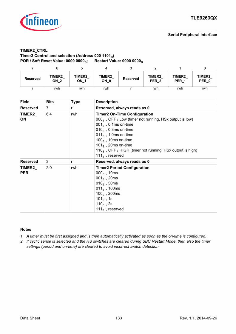
Data Sheet 133 Rev. 1.1, 2014-09-26
TLE9263QX
Serial Peripheral Interface
Notes1. A timer must be first assigned and is then automatically activated as soon as the on-time is configured.2. If cyclic sense is selected and the HS switches are cleared during SBC Restart Mode, then also the timer
settings (period and on-time) are cleared to avoid incorrect switch detection.
TIMER2_CTRLTimer2 Control and selection (Address 000 1101B)POR / Soft Reset Value: 0000 0000B; Restart Value: 0000 0000B
7 6 5 4 3 2 1 0
Reserved TIMER2_ON_2
TIMER2_ON_1
TIMER2_ON_0 Reserved TIMER2_
PER_2TIMER2_PER_1
TIMER2_PER_0
r
r rwh rwh rwh r rwh rwh rwh
Field Bits Type DescriptionReserved 7 r Reserved, always reads as 0TIMER2_ON
6:4 rwh Timer2 On-Time Configuration000B , OFF / Low (timer not running, HSx output is low)001B , 0.1ms on-time 010B , 0.3ms on-time011B , 1.0ms on-time100B , 10ms on-time101B , 20ms on-time110B , OFF / HIGH (timer not running, HSx output is high)111B , reserved
Reserved 3 r Reserved, always reads as 0TIMER2_PER
2:0 rwh Timer2 Period Configuration000B , 10ms001B , 20ms010B , 50ms011B , 100ms100B , 200ms101B , 1s110B , 2s111B , reserved

Data Sheet 134 Rev. 1.1, 2014-09-26
TLE9263QX
Serial Peripheral Interface
SW_SD_CTRLSwitch Shutdown Control (Address 001 0000B)POR / Soft Reset Value: 0000 0000B; Restart Value: 0xxx 0000B
7 6 5 4 3 2 1 0
Reserved HS_OV_SD_EN
HS_UV_SD_EN
HS_OV_UV_REC Reserved Reserved Reserved Reserved
r
r rw rw rw r r r r
Field Bits Type DescriptionReserved 7 r Reserved, always reads as 0HS_OV_SD_EN
6 rw Shutdown Disabling of HS1...4 in case of VSHS OV0B , shutdown enabled in case of VSHS OV1B , shutdown disabled in case of VSHS OV
HS_UV_SD_EN
5 rw Shutdown Disabling of HS1...4 in case of VSHS UV0B , shutdown enabled in case of VSHS UV1B , shutdown disabled in case of VSHS UV
HS_OV_UV_REC
4 rw Switch Recovery after Removal of VSHS OV/UV for HS1...40B , Switch recovery is disabled1B , Previous state before VSHS OV/UV is enabled after OV/UV
condition is removedReserved 3:0 r Reserved, always reads as 0
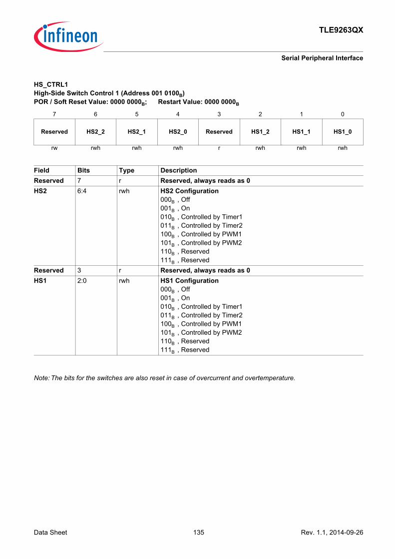
Data Sheet 135 Rev. 1.1, 2014-09-26
TLE9263QX
Serial Peripheral Interface
Note: The bits for the switches are also reset in case of overcurrent and overtemperature.
HS_CTRL1High-Side Switch Control 1 (Address 001 0100B)POR / Soft Reset Value: 0000 0000B; Restart Value: 0000 0000B
7 6 5 4 3 2 1 0
Reserved HS2_2 HS2_1 HS2_0 Reserved HS1_2 HS1_1 HS1_0
r
rw rwh rwh rwh r rwh rwh rwh
Field Bits Type DescriptionReserved 7 r Reserved, always reads as 0HS2 6:4 rwh HS2 Configuration
000B , Off001B , On010B , Controlled by Timer1011B , Controlled by Timer2100B , Controlled by PWM1101B , Controlled by PWM2110B , Reserved111B , Reserved
Reserved 3 r Reserved, always reads as 0HS1 2:0 rwh HS1 Configuration
000B , Off001B , On010B , Controlled by Timer1011B , Controlled by Timer2100B , Controlled by PWM1101B , Controlled by PWM2110B , Reserved111B , Reserved

Data Sheet 136 Rev. 1.1, 2014-09-26
TLE9263QX
Serial Peripheral Interface
Note: The bits for the switches are also reset in case of overcurrent and overtemperature.
HS_CTRL2High-Side Switch Control 2 (Address 001 0101B)POR / Soft Reset Value: 0000 0000B; Restart Value: 0000 0000B
7 6 5 4 3 2 1 0
Reserved HS4_2 HS4_1 HS4_0 Reserved HS3_2 HS3_1 HS3_0
r
r rwh rwh rwh r rwh rwh rwh
Field Bits Type DescriptionReserved 7 r Reserved, always reads as 0HS4 6:4 rwh HS4 Configuration
000B , Off001B , On010B , Controlled by Timer1011B , Controlled by Timer2100B , Controlled by PWM1101B , Controlled by PWM2110B , Reserved111B , Reserved
Reserved 3 r Reserved, always reads as 0HS3 2:0 rwh HS3 Configuration
000B , Off001B , On010B , Controlled by Timer1011B , Controlled by Timer2100B , Controlled by PWM1101B , Controlled by PWM2110B , Reserved111B , Reserved

Data Sheet 137 Rev. 1.1, 2014-09-26
TLE9263QX
Serial Peripheral Interface
Note: When selecting a filter time configuration, the user must make sure to also assign the respective timer to at least one HS switch during cyclic sense operation
GPIO_CTRLGPIO Configuration Control (Address 001 0111B)POR / Soft Reset Value: 0000 0000B; Restart Value: xxxx xxxxB
7 6 5 4 3 2 1 0
FO_DC_1 FO_DC_0 GPIO2_2 GPIO2_1 GPIO2_0 GPIO1_2 GPIO1_1 GPIO1_0
r
rw rw rw rw rw rw rw rw
Field Bits Type DescriptionFO_DC 7:6 rw Duty Cycle Configuration of FO3 (if selected)
00B , 20%01B , 10%10B , 5%11B , 2.5%
GPIO2 5:3 rw GPIO2 Configuration000B , FO3 selected001B , FO3 selected010B , FO3 selected011B , FO3 selected100B , OFF101B , Wake input enabled (16µs static filter)110B , Low-Side Switch ON111B , High-Side Switch ON
GPIO1 2:0 rw GPIO1 Configuration000B , FO2 selected001B , FO2 selected010B , FO2 selected011B , FO2 selected100B , OFF101B , Wake input enabled (16µs static filter)110B , Low-Side Switch ON111B , High-Side Switch ON
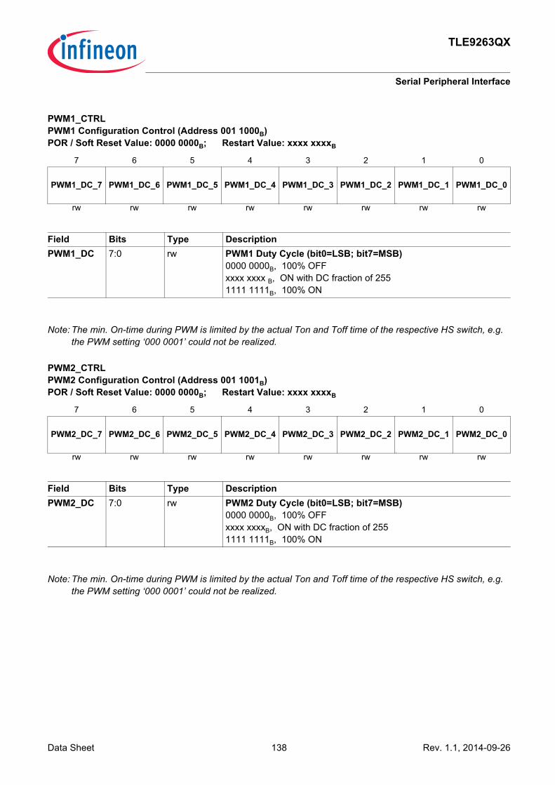
Data Sheet 138 Rev. 1.1, 2014-09-26
TLE9263QX
Serial Peripheral Interface
Note: The min. On-time during PWM is limited by the actual Ton and Toff time of the respective HS switch, e.g.
the PWM setting ‘000 0001’ could not be realized.
Note: The min. On-time during PWM is limited by the actual Ton and Toff time of the respective HS switch, e.g. the PWM setting ‘000 0001’ could not be realized.
PWM1_CTRLPWM1 Configuration Control (Address 001 1000B)POR / Soft Reset Value: 0000 0000B; Restart Value: xxxx xxxxB
7 6 5 4 3 2 1 0
PWM1_DC_7 PWM1_DC_6 PWM1_DC_5 PWM1_DC_4 PWM1_DC_3 PWM1_DC_2 PWM1_DC_1 PWM1_DC_0
r
rw rw rw rw rw rw rw rw
Field Bits Type DescriptionPWM1_DC 7:0 rw PWM1 Duty Cycle (bit0=LSB; bit7=MSB)
0000 0000B, 100% OFFxxxx xxxx B, ON with DC fraction of 2551111 1111B, 100% ON
PWM2_CTRLPWM2 Configuration Control (Address 001 1001B)POR / Soft Reset Value: 0000 0000B; Restart Value: xxxx xxxxB
7 6 5 4 3 2 1 0
PWM2_DC_7 PWM2_DC_6 PWM2_DC_5 PWM2_DC_4 PWM2_DC_3 PWM2_DC_2 PWM2_DC_1 PWM2_DC_0
r
rw rw rw rw rw rw rw rw
Field Bits Type DescriptionPWM2_DC 7:0 rw PWM2 Duty Cycle (bit0=LSB; bit7=MSB)
0000 0000B, 100% OFFxxxx xxxxB, ON with DC fraction of 255 1111 1111B, 100% ON

Data Sheet 139 Rev. 1.1, 2014-09-26
TLE9263QX
Serial Peripheral Interface
Note: The min. On-time during PWM is limited by the actual Ton and Toff time of the respective HS switch, e.g. the PWM setting ‘000 0001’ could not be realized.
Notes1. The SYS_STATUS_CTRL register is an exception for the default values, i.e. it will keep its configured value
also after a Soft Reset.2. This byte is intended for storing system configurations of the ECU by the microcontroller and is only accessible
in SBC Normal Mode. The byte is not accessible by the SBC and is also not cleared after Fail-Safe or SBC Restart Mode. It allows the microcontroller to quickly store system configuration without loosing the data.
PWM_FREQ_CTRLPWM Frequency Configuration Control (Address 001 1100B)POR / Soft Reset Value: 0000 0000B; Restart Value: 0000 0x0xB
7 6 5 4 3 2 1 0
Reserved Reserved Reserved Reserved Reserved PWM2_FREQ Reserved PWM1_FREQ
r
r r r r r rw r rw
Field Bits Type DescriptionReserved 7:3 r Reserved, always reads as 0PWM2_FREQ
2 rw PWM2 Frequency Selection0B , 200Hz configuration 1B , 400Hz configuration
Reserved 1 r Reserved, always reads as 0PWM1_FREQ
0 rw PWM1 Frequency Selection0B , 200Hz configuration 1B , 400Hz configuration
SYS_STATUS_CTRLSystem Status Control (Address 001 1110B)POR Value: 0000 0000B; Restart Value/Soft Reset Value: xxxx xxxxB
7 6 5 4 3 2 1 0
SYS_STAT_7 SYS_STAT_6 SYS_STAT_5 SYS_STAT_4 SYS_STAT_3 SYS_STAT_2 SYS_STAT_1 SYS_STAT_0
r
rw rw rw rw rw rw rw rw
Field Bits Type DescriptionSYS_STAT 7:0 rw System Status Control Byte (bit0=LSB; bit7=MSB)
Dedicated byte for system configuration, access only by microcontroller. Cleared after power up and Soft Reset

Data Sheet 140 Rev. 1.1, 2014-09-26
TLE9263QX
Serial Peripheral Interface
16.6 SPI Status Information RegistersREAD/CLEAR Operation (see also Chapter 16.3):• One 16-bit SPI command consist of two bytes:
- the 7-bit address and one additional bit for the register access mode and - following the data byteThe numbering of following bit definitions refers to the data byte and correspond to the bits D0...D7 and to the SPI bits 8...15 (see also figure).
• There are two different bit types:- ‘r’ = READ: read only bits (or reserved bits)- ‘rc’ = READ/CLEAR: readable and clearable bits
• Reading a register is done byte wise by setting the SPI bit 7 to “0” (= Read Only)• Clearing a register is done byte wise by setting the SPI bit 7 to “1”• SPI status registers are in general not cleared or changed automatically (an exception are the WD_FAIL bits).
This must be done by the microcontroller via SPI command
The registers are addressed wordwise.

Data Sheet 141 Rev. 1.1, 2014-09-26
TLE9263QX
Serial Peripheral Interface
16.6.1 General Status Registers
Notes1. The VCC1 undervoltage prewarning threshold VPW,f / VPW,r is a fixed threshold and independent of the VCC1
undervoltage reset thresholds.
SUP_STAT_2Supply Voltage Fail Status (Address 100 0000B)POR / Soft Reset Value: 0000 0000B; Restart Value: 0x0x xxxxB
7 6 5 4 3 2 1 0
Reserved VS_UV Reserved VCC3_OC VCC3_UV VCC3_OT VCC1_OV VCC1_WARN
r
r rc r rc rc rc rc rc
Field Bits Type DescriptionReserved 7 r Reserved, always reads as 0VS_UV 6 rc VS Under-Voltage Detection (VS,UV)
0B , No VS under voltage detected1B , VS under voltage detected
Reserved 5 r Reserved, always reads as 0VCC3_OC 4 rc VCC3 Over Current Detection
0B , No OC1B , OC detected
VCC3_UV 3 rc VCC3 Under Voltage Detection 0B , No VCC3 UV detection1B , VCC3 UV Fail detected
VCC3_OT 2 rc VCC3 Over Temperature Detection0B , No over temperature1B , VCC3 over temperature detected
VCC1_OV
1 rc VCC1 Over Voltage Detection (VCC1,OV,r)0B , No VCC1 over voltage warning1B , VCC1 over voltage detected
VCC1_WARN
0 rc VCC1 Undervoltage Prewarning (VPW,f)0B , No VCC1 undervoltage prewarning1B , VCC1 undervoltage prewarning detected

Data Sheet 142 Rev. 1.1, 2014-09-26
TLE9263QX
Serial Peripheral Interface
Notes1. The MSB of the POR/Soft Reset value is marked as ‘y’: the default value of the POR bit is set after Power-on
reset (POR value = 1000 0000). However it will be cleared after a SBC Soft Reset command (Soft Reset value = 0000 0000).
2. During Sleep Mode, the bits VCC1_SC,VCC1_OV and VCC1_UV will not be set when VCC1 is off3. The VCC1_UV bit is never updated in SBC Restart Mode, in SBC Init Mode it is only updated after RO was
released for the first time, it is always updated in SBC Normal and Stop Mode, and it is always updated in any SBC modes in a VCC1_SC condition (after VCC1_UV = 1 for >4ms).
SUP_STAT_1Supply Voltage Fail Status (Address 100 0001B)POR / Soft Reset Value: y000 0000B; Restart Value: xxxx xx0xB
7 6 5 4 3 2 1 0
POR VSHS_UV VSHS_OV VCC2_OT VCC2_UV VCC1_SC VCC1_UV_FS VCC1_UV
r
rc rc rc rc rc rc rc rc
Field Bits Type DescriptionPOR 7 rc Power-On Reset Detection
0B , No POR1B , POR occurred
VSHS_UV 6 rc VSHS Under-Voltage Detection (VSHS,UVD)0B , No VSHS-UV1B , VSHS-UV detected
VSHS_OV 5 rc VSHS Over-Voltage Detection (VSHS,OVD)0B , No VSHS-OV1B , VSHS-OV detected
VCC2_OT 4 rc VCC2 Over Temperature Detection0B , No over temperature1B , VCC2 over temperature detected
VCC2_UV 3 rc VCC2 Under Voltage Detection (VCC2,UV,f)0B , No VCC2 Under voltage1B , VCC2 under voltage detected
VCC1_SC 2 rc VCC1 Short to GND Detection (<Vrtx for t>4ms after switch on)0B , No short1B , VCC1 short to GND detected
VCC1_UV_FS
1 rc VCC1 UV-Detection (due to Vrtx reset)0B , No Fail-Safe Mode entry due to 4th consecutive VCC1_UV1B , Fail-Safe Mode entry due to 4th consecutive VCC1_UV
VCC1_UV 0 rc VCC1 UV-Detection (due to Vrtx reset)0B , No VCC1_UV detection1B , VCC1 UV-Fail detected

Data Sheet 143 Rev. 1.1, 2014-09-26
TLE9263QX
Serial Peripheral Interface
Note: TSD1 and TSD2 are not reset automatically, even if the temperature pre warning or TSD1 OT condition is not present anymore. Also TSD2 is not reset.
THERM_STATThermal Protection Status (Address 100 0010B)POR / Soft Reset Value: 0000 0000B; Restart Value: 0000 0xxxB
7 6 5 4 3 2 1 0
Reserved Reserved Reserved Reserved Reserved TSD2 TSD1 TPW
r
r r r r r rc rc rc
Field Bits Type DescriptionReserved 7:3 r Reserved, always reads as 0TSD2 2 rc TSD2 Thermal Shut-Down Detection
0B , No TSD2 event1B , TSD2 OT detected - leading to SBC Fail-Safe Mode
TSD1 1 rc TSD1 Thermal Shut-Down Detection0B , No TSD1 fail1B , TSD1 OT detected
TPW 0 rc Thermal Pre Warning0B , No Thermal Pre warning1B , Thermal Pre warning detected

Data Sheet 144 Rev. 1.1, 2014-09-26
TLE9263QX
Serial Peripheral Interface
Notes1. The bits DEV_STAT show the status of the device before it went through Restart. Either the device came from
regular Sleep Mode (‘10’) or a failure (‘01’ - SBC Restart or SBC Fail-Safe Mode: WD fail, TSD2 fail, VCC_UV fail or VCC1_OV if bit VCC1_OV_RST is set) occurred. Failure is also an illegal command from SBC Stop to SBC Sleep Mode or going to SBC Sleep Mode without activation of any wake source. Coming from SBC Sleep Mode (‘10’) will also be shown if there was a trial to enter SBC Sleep Mode without having cleared all wake flags before.
2. The WD_FAIL bits are configured as a counter and are the only status bits, which are cleared automatically by the SBC. They are cleared after a successful watchdog trigger and when the watchdog is stopped (also in SBC Sleep and Fail-Safe Mode unless it was reached due to a watchdog failure). See also Chapter 14.1.
3. The SPI_FAIL bit is cleared only by SPI command4. In case of Config 2/4 the WD_Fail counter is frozen in case of WD trigger failure until a successful WD trigger.5. If CFG = ‘0’ then a 1st watchdog failure will not trigger the FO outputs or the FAILURE bit but only force the
SBC into SBC Restart Mode.
DEV_STATDevice Information Status (Address 100 0011B)POR / Soft Reset Value: 0000 0000B; Restart Value: xx00 xxxxB
7 6 5 4 3 2 1 0
DEV_STAT_1 DEV_STAT_0 Reserved Reserved WD_FAIL_1 WD_FAIL_0 SPI_FAIL FAILURE
r
rc rc r r rh rh rc rc
Field Bits Type DescriptionDEV_STAT 7:6 rc Device Status before Restart Mode
00B , Cleared (Register must be actively cleared)01B , Restart due to failure (WD fail, TSD2, VCC1_UV); also after a
wake from Fail-Safe Mode10B , Sleep Mode11B , Reserved
Reserved 5:4 r Reserved, always reads as 0WD_FAIL 3:2 rh Number of WD-Failure Events (1/2 WD failures depending on
CFG)00B , No WD Fail01B , 1x WD Fail, FOx activation - Config 2 selected10B , 2x WD Fail, FOx activation - Config 1 / 3 / 4 selected11B , Reserved (never reached)
SPI_FAIL 1 rc SPI Fail Information0B , No SPI fail1B , Invalid SPI command detected
FAILURE 0 rc Activation of Fail Output FO0B , No Failure1B , Failure occurred

Data Sheet 145 Rev. 1.1, 2014-09-26
TLE9263QX
Serial Peripheral Interface
Notes1. The VCAN_UV comparator is enabled if the mode bit CAN_1 = ‘1’, i.e. in CAN Normal or CAN Receive Only
Mode.
BUS_STAT_1Bus Communication Status (Address 100 0100B)POR / Soft Reset Value: 0000 0000B; Restart Value: 0xx0 0xxxB
7 6 5 4 3 2 1 0
Reserved LIN1_FAIL_1 LIN1_FAIL_0 Reserved Reserved CAN_FAIL_1 CAN_FAIL_0 VCAN_UV
r
r rc rc r r rc rc rc
Field Bits Type DescriptionReserved 7 r Reserved, always reads as 0LIN1_FAIL 6:5 rc LIN1 Failure Status
00B , No error01B , LIN1 TSD 10B , LIN1_TXD_DOM: TXD dominant time out for more than 20ms11B , LIN1_BUS_DOM: BUS dominant time out for more than 20ms
Reserved 4:3 r Reserved, always reads as 0CAN_FAIL 2:1 rc CAN Failure Status
00B , No error01B , CAN TSD 10B , CAN_TXD_DOM: TXD dominant time out for more than 4ms11B , CAN_BUS_DOM: BUS dominant time out for more than 4ms
VCAN_UV 0 rc Under Voltage CAN Bus Supply0B , Normal operation1B , CAN Supply under voltage detected. Transmitter disabled

Data Sheet 146 Rev. 1.1, 2014-09-26
TLE9263QX
Serial Peripheral Interface
Note: CAN and LINx Recovery Conditions: 1.) TXD Time Out: TXD goes High or transmitter is set to wake capable or switched off; 2.). Bus dominant time out: Bus will become recessive or transceiver is set to wake capable or switched off.3.) Supply under voltage: as soon as the threshold is crossed again, i.e. VSHS > VS_UV for LINx and VCAN > VCAN_UV for CAN4.) In all cases (also for TSD shutdown): to enable the Bus transmission again, TXD needs to be HIGH for a certain time (transmitter enable time).
BUS_STAT_2Bus Communication Status (Address 100 0101B)POR / Soft Reset Value: 0000 0000B; Restart Value: 0000 0xx0B
7 6 5 4 3 2 1 0
Reserved Reserved Reserved Reserved Reserved LIN2_FAIL_1 LIN2_FAIL_0 Reserved
r
r r r r r rc rc r
Field Bits Type DescriptionReserved 7:3 r Reserved, always reads as 0LIN2_FAIL 2:1 rc LIN2 Failure Status
00B , No error01B , LIN2 TSD shutdown10B , LIN2_TXD_DOM: TXD dominant time out for more than 20ms11B , LIN2_BUS_DOM: BUS dominant time out for more than 20ms
Reserved 0 r Reserved, always reads as 0

Data Sheet 147 Rev. 1.1, 2014-09-26
TLE9263QX
Serial Peripheral Interface
Note: The respective wake source bit will also be set when the device is woken from SBC Fail-Safe Mode
WK_STAT_1Wake-up Source and Information Status (Address 100 0110B)POR / Soft Reset Value: 0000 0000B; Restart Value: xxxx 0xxxB
7 6 5 4 3 2 1 0
LIN2_WU LIN1_WU CAN_WU TIMER_WU Reserved WK3_WU WK2_WU WK1_WU
r
rc rc rc rc r rc rc rc
Field Bits Type DescriptionLIN2_WU 7 rc Wake up via LIN2 Bus
0B , No Wake up1B , Wake up
LIN1_WU 6 rc Wake up via LIN1 Bus0B , No Wake up1B , Wake up
CAN_WU 5 rc Wake up via CAN Bus0B , No Wake up1B , Wake up
TIMER_WU 4 rc Wake up via TimerX0B , No Wake up1B , Wake up
Reserved 3 r Reserved, always reads as 0WK3_WU 2 rc Wake up via WK3
0B , No Wake up1B , Wake up
WK2_WU 1 rc Wake up via WK20B , No Wake up1B , Wake up
WK1_WU 0 rc Wake up via WK10B , No Wake up1B , Wake up

Data Sheet 148 Rev. 1.1, 2014-09-26
TLE9263QX
Serial Peripheral Interface
WK_STAT_2Wake-up Source and Information Status (Address 100 0111B)POR / Soft Reset Value: 0000 0000B; Restart Value: 00xx 0000B
7 6 5 4 3 2 1 0
Reserved Reserved GPIO2_WU GPIO1_WU Reserved Reserved Reserved Reserved
r
r r rc rc r r r r
Field Bits Type DescriptionReserved 7:6 r Reserved, always reads as 0GPIO2_WU 5 rc Wake up via GPIO2
0B , No Wake up1B , Wake up
GPIO1_WU 4 rc Wake up via GPIO10B , No Wake up1B , Wake up
Reserved 3:0 r Reserved, always reads as 0

Data Sheet 149 Rev. 1.1, 2014-09-26
TLE9263QX
Serial Peripheral Interface
Note: GPIOx_LVL is updated in SBC Normal and Stop Mode if configured as wake input, low-side switch or high-side switch. In cyclic sense or wake mode, the registers contain the sampled level, i.e. the registers are updated after every sampling. The GPIOs are not capable of cyclic sensing.If selected as GPIO then the respective level is shown even if configured as low-side or high-side.
WK_LVL_STATWK Input Level (Address 100 1000B)POR / Soft Reset Value: xx00 0xxxB; Restart Value: xxxx 0xxxB
7 6 5 4 3 2 1 0
SBC_DEV_LVL CFGP GPIO2_LVL GPIO1_LVL Reserved WK3_LVL WK2_LVL WK1_LVL
r
r r r r r r r r
Field Bits Type DescriptionSBC_DEV_LVL
7 r Status of SBC Operating Mode at FO3/TEST Pin0B , User Mode activated 1B , SBC Software Development Mode activated
CFGP 6 r Device Configuration Status0B , No external pull-up resistor connected on INT (Config 2/4)1B , External pull-up resistor connected on INT (Config 1/3)
GPIO2_LVL 5 r Status of GPIO2 (if selected as GPIO)0B , Low Level (=0)1B , High Level (=1)
GPIO1_LVL 4 r Status of GPIO1 (if selected as GPIO)0B , Low Level (=0)1B , High Level (=1)
Reserved 3 r Reserved, always reads as 0WK3_LVL 2 r Status of WK3
0B , Low Level (=0)1B , High Level (=1)
WK2_LVL 1 r Status of WK20B , Low Level (=0)1B , High Level (=1)
WK1_LVL 0 r Status of WK10B , Low Level (=0)1B , High Level (=1)

Data Sheet 150 Rev. 1.1, 2014-09-26
TLE9263QX
Serial Peripheral Interface
Note: The OC/OT bit might be set for VPOR,f < VS < 5.5V (see also Chapter 4.2)
HS_OC_OT_STATHigh-Side Switch Overload Status (Address 101 0100B)POR / Soft Reset Value: 0000 0000B; Restart Value: 0000 xxxxB
7 6 5 4 3 2 1 0
Reserved Reserved Reserved Reserved HS4_OC_OT HS3_OC_OT HS2_OC_OT HS1_OC_OT
r
r r r r rc rc rc rc
Field Bits Type DescriptionReserved 7:4 r Reserved, always reads as 0HS4_OC_OT 3 rc Over-Current & Over-Temperature Detection HS4
0B , No OC or OT1B , OC or OT detected
HS3_OC_OT 2 rc Over-Current & Over-Temperature Detection HS30B , No OC or OT1B , OC or OT detected
HS2_OC_OT 1 rc Over-Current & Over-Temperature Detection HS20B , No OC or OT1B , OC or OT detected
HS1_OC_OT 0 rc Over-Current & Over-Temperature Detection HS10B , No OC or OT1B , OC or OT detected

Data Sheet 151 Rev. 1.1, 2014-09-26
TLE9263QX
Serial Peripheral Interface
HS_OL_STATHigh-Side Switch Open-Load Status (Address 101 0101B)POR / Soft Reset Value: 0000 0000B; Restart Value: 0000 xxxxB
7 6 5 4 3 2 1 0
Reserved Reserved Reserved Reserved HS4_OL HS3_OL HS2_OL HS1_OL
r
r r r r rc rc rc rc
Field Bits Type DescriptionReserved 7:4 r Reserved, always reads as 0HS4_OL 3 rc Open-Load Detection HS4
0B , No OL1B , OL detected
HS3_OL 2 rc Open-Load Detection HS30B , No OL1B , OL detected
HS2_OL 1 rc Open-Load Detection HS20B , No OL1B , OL detected
HS1_OL 0 rc Open-Load Detection HS10B , No OL1B , OL detected

Data Sheet 152 Rev. 1.1, 2014-09-26
TLE9263QX
Serial Peripheral Interface
16.6.2 Family and Product Information Register
Notes1. The actual default register value after POR, Soft Reset or Restart of PROD will depend on the respective
product. Therefore the value ‘y’ is specified.2. SWK = Selective Wake feature in CAN Partial Networking standard
FAM_PROD_STATFamily and Product Identification Register (Address 111 1110B)POR / Soft Reset Value: 0011 yyyy B; Restart Value: 0011 yyyyB
7 6 5 4 3 2 1 0
FAM_3 FAM_2 FAM_1 FAM_0 PROD_3 PROD_2 PROD_1 PROD_0
r
r r r r r r r r
Field Bits Type DescriptionFAM 7:4 r SBC Family Identifier (bit4=LSB; bit7=MSB)
0 0 01B, Driver SBC Family0 0 10B, DC/DC-SBC Family 0 0 11B, Mid-Range SBC Family x x x xB, reserved for future products
PROD 3:0 r SBC Product Identifier (bit0=LSB; bit3=MSB)0 0 0 0B, TLE9260QX (5V, no LIN, no VCC3, no SWK)0 1 0 0B, TLE9261QX (5V, no LIN, VCC3, no SWK)1 0 0 0B, TLE9262QX (5V, 1 LIN, VCC3, no SWK)1 1 0 0B, TLE9263QX (5V, 2 LIN, VCC3, no SWK)

Data Sheet 153 Rev. 1.1, 2014-09-26
TLE9263QX
Serial Peripheral Interface
16.7 Electrical Characteristics
Table 29 Electrical CharacteristicsVS = 5.5 V to 28 V, Tj = -40 °C to +150 °C, all voltages with respect to ground, positive current flowing into pin(unless otherwise specified)Parameter Symbol Values Unit Note /
Test ConditionNumber
Min. Typ. Max.SPI frequencyMaximum SPI frequency fSPI,max – – 4.0 MHz 1) P_16.7.1SPI Interface; Logic Inputs SDI, CLK and CSNH-input Voltage Threshold VIH – – 0.7*
VCC1
V – P_16.7.2
L-input Voltage Threshold VIL 0.3*VCC1
– – V – P_16.7.3
Hysteresis of input Voltage VIHY – 0.12*VCC1
– V 1) P_16.7.4
Pull-up Resistance at pin CSN RICSN 20 40 80 kΩ VCSN = 0.7 x VCC1 P_16.7.5Pull-down Resistance at pin SDI and CLK
RICLK/SDI 20 40 80 kΩ VSDI/CLK = 0.2 x VCC1
P_16.7.6
Input Capacitance at pin CSN, SDI or CLK
CI – 10 – pF 1) P_16.7.7
Logic Output SDOH-output Voltage Level VSDOH VCC1 -
0.4VCC1 -0.2
– V IDOH = -1.6 mA P_16.7.8
L-output Voltage Level VSDOL – 0.2 0.4 V IDOL = 1.6 mA P_16.7.9Tristate Leakage Current ISDOLK -10 – 10 µA VCSN = VCC1;
0 V < VDO < VCC1
P_16.7.10
Tristate Input Capacitance CSDO – 10 15 pF 1) P_16.7.11Data Input Timing1)
Clock Period tpCLK 250 – – ns – P_16.7.12Clock High Time tCLKH 125 – – ns – P_16.7.13Clock Low Time tCLKL 125 – – ns – P_16.7.14Clock Low before CSN Low tbef 125 – – ns – P_16.7.15CSN Setup Time tlead 250 – – ns – P_16.7.16CLK Setup Time tlag 250 – – ns – P_16.7.17Clock Low after CSN High tbeh 125 – – ns – P_16.7.18SDI Set-up Time tDISU 100 – – ns – P_16.7.19SDI Hold Time tDIHO 50 – – ns – P_16.7.20Input Signal Rise Time at pin SDI, CLK and CSN
trIN – – 50 ns – P_16.7.21
Input Signal Fall Time at pin SDI, CLK and CSN
tfIN – – 50 ns – P_16.7.22
Delay Time for Mode Changes2)
tDel,Mode – – 6 µs includes internal oscillator tolerance
P_16.7.23
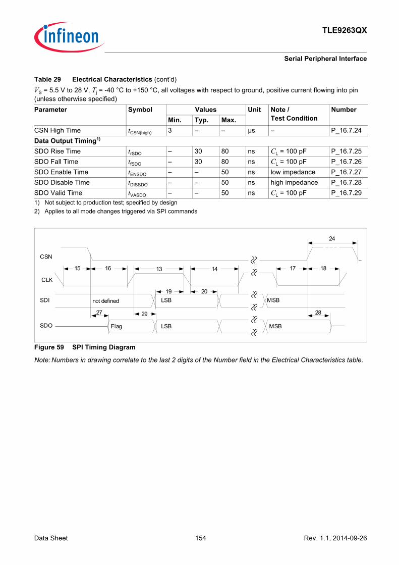
Data Sheet 154 Rev. 1.1, 2014-09-26
TLE9263QX
Serial Peripheral Interface
Figure 59 SPI Timing Diagram
Note: Numbers in drawing correlate to the last 2 digits of the Number field in the Electrical Characteristics table.
CSN High Time tCSN(high) 3 – – µs – P_16.7.24Data Output Timing1)
SDO Rise Time trSDO – 30 80 ns CL = 100 pF P_16.7.25SDO Fall Time tfSDO – 30 80 ns CL = 100 pF P_16.7.26SDO Enable Time tENSDO – – 50 ns low impedance P_16.7.27SDO Disable Time tDISSDO – – 50 ns high impedance P_16.7.28SDO Valid Time tVASDO – – 50 ns CL = 100 pF P_16.7.29 1) Not subject to production test; specified by design2) Applies to all mode changes triggered via SPI commands
Table 29 Electrical Characteristics (cont’d)VS = 5.5 V to 28 V, Tj = -40 °C to +150 °C, all voltages with respect to ground, positive current flowing into pin(unless otherwise specified)Parameter Symbol Values Unit Note /
Test ConditionNumber
Min. Typ. Max.
CSN
CLK
SDI
SDO
1413
not defined LSB MSB
Flag LSB MSB
16
27 29
19
17
28
24
20
15 18

Data Sheet 155 Rev. 1.1, 2014-09-26
TLE9263QX
Application Information
17 Application Information
17.1 Application Diagram
Note: The following information is given as a hint for the implementation of the device only and shall not be regarded as a description or warranty of a certain functionality, condition or quality of the device.
Figure 60 Simplified Application Diagram
C1
R13
C15
VSHS
LIN1
S1
VBAT
C11
R10
CANH
C12
R11
CANL
R2
VSS
VDDCSNCLKSDISDO
µC
INT
CSNCLK
SDOSDI
FOx
VCC1
C4
VCC1
C5
WK1
HS1
VS
Reset
INT
RO
VCAN
GND
Q1VCC
GND
IC1
VS
LOGICState
Machine
Application _information_TLE9263 .vsd
VS
T1
CANH
CANL
CAN cell
VBAT
VBAT VS
TLE9263
VS
VCC3REF
Q2
LIN1LIN cell
HS2
HS3
VSHS
HS4
LH
VCC2
WK3
WK2
R1
S2
R4
S3
R6
R5R3
Hall1
Hall2
Q1
Q2
Q1
Q2
D1
C7
R8
D3
Other loads , e.g. sensor , opamp, ...
C8
R7
D4
R14
C16
LIN2LIN cell
VSHS
LIN2
TxD LIN2RxD LIN2TxD CANRxD CAN
TxD LIN2RxD LIN2TxD CANRxD CAN
TxD LIN1RxD LIN1
TxD LIN1RxD LIN1
VCC2
VSHS
VSHS
VSHS
VSHS
D2 C2
C3
Note: The external capacitance on FO3/TEST must be <=10nF in oder to ensure proper detection of SBC Development Mode und SBC user mode operation
T2
C13
R12VCC3
VCC3BVCC3SH
C14
C9
C10
C6
VCC2
D6
D5
R9
C17
C18

Data Sheet 156 Rev. 1.1, 2014-09-26
TLE9263QX
Application Information
Note: Unused outputs are recommended to be left unconnected on the application board. If unused output pins are routed to an external connector which leaves the ECU, then these pins should have provision for a zero ohm jumper (depopulated if unused) or ESD protection.
Table 30 Bill of Material for Simplified Application DiagramRef. Typical Value Purpose / CommentCapacitancesC1 68µF Buffering capacitor to cut off battery spikes, depending on applicationC2 100nF EMC, blocking capacitorC3 22µF Buffering capacitor to cut off battery spikes from VSHS as separate supply
input; Depending on application, only needed if VSHS is not connected to VS;
C4 2.2µF low ESR As required by application, min. 470nF for stabilityC5 100nF ceramic Spike filtering, improve stability of supply for microcontroller;
not needed for SBCC6 2.2µF low ESR Blocking capacitor, min. 470nF for stability;
if used for CAN supply place a 100nF ceramic capacitor in addition very close to VCAN pin for optimum EMC behavior
C7 33nF As required by application, mandatory protection for off-board connectionsC8 33nF As required by application, mandatory protection for off-board connectionsC17 47pF Only required in case of off-board connection to optimize EMC behavior,
place close to pinC18 47pF Only required in case of off-board connection to optimize EMC behavior,
place close to pinC9 10nF Spike filtering, as required by application, mandatory protection for off-board
connections (see also Simplified Application Diagram with the Alternate Measurement Function)
C10 10nF Spike filtering, as required by application, mandatory protection for off-board connections
C11 10nF Spike filtering, as required by application, mandatory protection for off-board connections
C12 4.7nF / OEM dependent Split termination stabilityC13 10µF low ESR Stability of VCC3, e.g. Murata 10 µF/10 V GCM31CR71A106K64LC14 47nF Only required in case of off-board connection to optimize EMC behavior,
place close to connectorC15 1nF / OEM dependent LIN master terminationC16 1nF / OEM dependent LIN master terminationResistancesR1 10kΩ Wetting current of the switch, as required by applicationR2 10kΩ Limit the WK pin current, e.g. for ISO pulsesR3 10kΩ Wetting current of the switch, as required by applicationR4 10kΩ Limit the WK pin current, e.g. for ISO pulsesR5 10kΩ Wetting current of the switch, as required by applicationR6 10kΩ Limit the WK pin current, e.g. for ISO pulses
Data Sheet 157 Rev. 1.1, 2014-09-26
TLE9263QX
Application Information
Note: This is a simplified example of an application circuit. The function must be verified in the real application.
R7 depending on LED config. LED current limitation, as required by applicationR8 depending on LED config. LED current limitation, as required by applicationR9 47kΩ Selection of hardware configuration 1/3, i.e. in case of WD failure SBC
Restart Mode is entered. If not connected, then hardware configuration 2/4 is selected
R10 60Ω / OEM dependent CAN bus terminationR11 60Ω / OEM dependent CAN bus terminationR12 1Ω shunt, depending on
required current limitation or load sharing ratio
Sense shunt for ICC3 current limitation (configured to typ. 235mA with 1Ω shunt) for stand-alone configuration;Setting of load sharing ratio (here ICC3/ICC1 = 1) in load sharing configuration.
R13 1kΩ / OEM dependent LIN master termination (if configured as a LIN master)R14 1kΩ / OEM dependent LIN master termination (if configured as a LIN master)R15 10kΩ WK1 pin current limitation, e.g. for ISO pulses, for alternate measurement
function (see also Simplified Application Diagram with the Alternate Measurement Function)
R16 depending on application and microcontroller
Voltage Divider resistor to adjust measurement voltage to microcontroller ADC input range (see also Simplified Application Diagram with the Alternate Measurement Function)
R17 depending on application and microcontroller
Voltage Divider resistor to adjust measurement voltage to microcontroller ADC input range (see also Simplified Application Diagram with the Alternate Measurement Function)
Active ComponentsD1 e.g. BAS 3010A, Infineon Reverse polarity protection for VS supply pinsD2 e.g. BAS 3010A, Infineon Reverse polarity protection for VSHS supply pin; if separate supplies are not
needed, then connect VSHS to VS pinsD3 LED As required by application, configure series resistor accordinglyD4 LED As required by application, configure series resistor accordinglyD5 e.g. BAS70 Requested by LIN standard; reverse polarity protection of networkD6 e.g. BAS70 Requested by LIN standard; reverse polarity protection of networkT1 e.g. BCR191W High active FO controlT2 BCP 52-16, Infineon Power element of VCC3, current limit or load sharing ratio to be configured
via shunt MJD 253, ON Semi Alternative power element of VCC3
µC e.g. TC2xxx Microcontroller
Table 30 Bill of Material for Simplified Application Diagram (cont’d)
Ref. Typical Value Purpose / Comment

Data Sheet 158 Rev. 1.1, 2014-09-26
TLE9263QX
Application Information
Figure 61 Simplified Application Diagram with the Alternate Measurement Function via WK1 and WK2
Note: This is a very simplified example of an application circuit. The function must be verified in the real application.WK1 must be connected to signal to be measured and WK2 is the output to the microcontroller supervision function. The maximum current into WK1 must be <500uA. The minimum current into WK1 should be >5uA to ensure proper operation.
C1e.g.
470uF
C2
VSS
VDDCSNCLKSDISDO
µC
TxD CANRxD CAN
INT
CSNCLK
SDOSDI
TxD CANRxD CAN
VCC1
C4
VCC1
C5
WK1
VS
Reset
INT
RO
GND
VS
LOGICState
Machine
VBAT
VBAT VS
TLE9263
WK2
R6
ADC_xVbat_uC
D1
D2
≥10kC9≥10n
Vbat_uC R16
R17
max. 500uA
ISO Pulse protection
S1
TxD LIN1RxD LIN1
TxD LIN1RxD LIN1
Note:Max. WK1 input current shall be be limited to 500µA to ensure accuracy and proper operation ;
TxD LIN2RxD LIN2
TxD LIN2RxD LIN2

Data Sheet 159 Rev. 1.1, 2014-09-26
TLE9263QX
Application Information
17.2 ESD Tests
Note: Tests for ESD robustness according to IEC61000-4-2 “gun test” (150pF, 330Ω) will been performed. The results and test condition will be available in a test report. The target values for the test are listed in Table 31 below.
EMC and ESD susceptibility tests according to SAE J2962-2 (2010) have been performed. Tested by external test house (UL LLC, Test report Nr. 2013-474A)
Table 31 ESD “Gun Test”Performed Test Result Unit RemarksESD at pin CANH, CANL, LIN, VS, WK1..3, HSx, VCC2, VCC3 versus GND
>6 kV 1)2)positive pulse
1)ESD Test “Gun Test” is specified with external components for pins VS, WK1..3, HSx, VCC3 and VCC2. See the application diagram in Chapter 17.1 for more information.2) ESD susceptibility “ESD GUN” according LIN EMC 1.3 Test Specification, Section 4.3 (IEC 61000-4-2). Tested by external
test house (IBEE Zwickau, EMC Test report Nr. 07-10-13)
ESD at pin CANH, CANL, LIN, VS, WK1..3, HSx, VCC2, VCC3 versus GND
< -6 kV 1)2)negative pulse
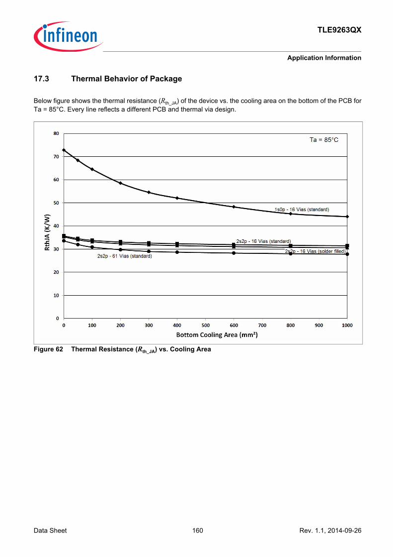
Data Sheet 160 Rev. 1.1, 2014-09-26
TLE9263QX
Application Information
17.3 Thermal Behavior of Package
Below figure shows the thermal resistance (Rth_JA) of the device vs. the cooling area on the bottom of the PCB forTa = 85°C. Every line reflects a different PCB and thermal via design.
Figure 62 Thermal Resistance (Rth_JA) vs. Cooling Area

Data Sheet 161 Rev. 1.1, 2014-09-26
TLE9263QX
Application Information
Figure 63 Board Setup
Board setup is defined according to JESD 51-2,-5,-7. Board: 76.2x114.3x1.5mm³ with 2 inner copper layers (35µm thick), with thermal via array under the exposed padcontacting the first inner copper layer and 300mm2 cooling area on the bottom layer (70µm).
PCB (top view) PCB (bottom view) Detail SolderArea
1,5
mm
1,5
mm
70µm modelled (traces)35µm, 90% metalization*
35µm, 90% metalization*
70µm / 5% metalization + cooling area*: means percentual Cu metalization on each layer
Cross Section (JEDEC 1s0p) with Cooling AreaCross Section (JEDEC 2s2p) with Cooling Area

Data Sheet 162 Rev. 1.1, 2014-09-26
TLE9263QX
Package Outlines
18 Package Outlines
Figure 64 PG-VQFN-48-31
Note: For assembly recommendations please also refer to the documents "Recommendations for Board Assembly (VQFN and IQFN)" and "VQFN48 Layout Hints" on the Infineon website (www.infineon.com).
The PG-VQFN-48-31 package is a leadless exposed pad power package featuring Lead Tip Inspection (LTI) tosupport Automatic Optical Inspection (AOI).
Green Product (RoHS compliant)To meet the world-wide customer requirements for environmentally friendly products and to be compliant withgovernment regulations the device is available as a green product. Green products are RoHS-Compliant (i.ePb-free finish on leads and suitable for Pb-free soldering according to IPC/JEDEC J-STD-020).
PG-VQFN-48-29, -31-PO V03
7±0.1A
6.8
7±0.
1
B
11 x 0.5 = 5.5
0.5
0.5±
0.07
0.1±
0.05
0.15
±0.0
5 (6)
(5.2
)
0.9 MAX.
(0.65)
+0.031)
2)
48x0.08
(0.2)
0.05 MAX.C
(5.2)
(6)
0.1±0.03
±0.050.23M
48x0.1 A B C
1) Vertical burr 0.03 max., all sides2) This four metal areas have exposed diepad potential
Index Marking
SEAT
ING
PLA
NE
Index Marking
6.8
12 1
13
24
25 36
(0.35)
37
48
0.4 x 45°
For further information on alternative packages, please visit our website:http://www.infineon.com/packages. Dimensions in mm

Data Sheet 163 Rev. 1.1, 2014-09-26
TLE9263QX
Revision History
19 Revision History
Table 32 Revision HistoryRevision Date ChangesRev 1.1 2014-09-26 Initial Release

Edition 2014-09-26Published byInfineon Technologies AG81726 Munich, Germany© 2014 Infineon Technologies AGAll Rights Reserved.
Legal DisclaimerThe information given in this document shall in no event be regarded as a guarantee of conditions or characteristics. With respect to any examples or hints given herein, any typical values stated herein and/or any information regarding the application of the device, Infineon Technologies hereby disclaims any and all warranties and liabilities of any kind, including without limitation, warranties of non-infringement of intellectual property rights of any third party.
InformationFor further information on technology, delivery terms and conditions and prices, please contact the nearest Infineon Technologies Office (www.infineon.com).
WarningsDue to technical requirements, components may contain dangerous substances. For information on the types in question, please contact the nearest Infineon Technologies Office.Infineon Technologies components may be used in life-support devices or systems only with the express written approval of Infineon Technologies, if a failure of such components can reasonably be expected to cause the failure of that life-support device or system or to affect the safety or effectiveness of that device or system. Life support devices or systems are intended to be implanted in the human body or to support and/or maintain and sustain and/or protect human life. If they fail, it is reasonable to assume that the health of the user or other persons may be endangered.