Synthesis, Optical and Ferroelectric Properties of PZT ...
40
1 Synthesis, Optical and Ferroelectric Properties of PZT Thin Films: A Experimental and Theoretical Investigation D.S.L. Pontes, 1,2 L. Gracia, 1 F.M. Pontes, 2 A. Beltrán 1 , J. Andrés 1 and E. Longo 3 1 Departament de Química Física i Analítica, Universitat Jaume I, Campus de Riu Sec, Castelló E-12080, Spain 2 Instituto de Química, UNESP CEP17033-360 Bauru, Brazil 3 LIEC, Instituto de Química, UNESP, P.O. Box 355, 14800-900, Araraquara, SP, Brazil Abstract PbZr 0.40 Ti 0.60 O 3 (PZT40/60) thin films with ferroelectric and dielectric properties have been grown on Pt/Ti/SiO 2 /Si and LaAlO 3 (100) substrates using the chemical solution deposition method. These films have been characterized by different techniques such X- ray diffraction (XRD), Raman, infrared and optical transmittance measurements. The transmittance curve of the PZT40/60 thin films on a LaAlO 3 (100) substrate showed an optical band gap of 4.03 and 3.10 eV for the direct and indirect transition processes, respectively. To complement experimental data, first principle calculations at the DFT- B3LYP level were performed on periodic model systems of PbTiO 3 and PZT40/60 to provide an insight into structural, optical and electronic behavior. The band gap of the PZT40/60 system for PbO and ZrO 2 terminations is in agreement with trends of experimental data and results in smaller values than the band gap calculated for the PbTiO 3 system.
Transcript of Synthesis, Optical and Ferroelectric Properties of PZT ...

1
Synthesis, Optical and Ferroelectric Properties of PZT Thin Films: A
Experimental and Theoretical Investigation
D.S.L. Pontes,
1,2 L. Gracia,
1 F.M. Pontes,
2 A. Beltrán
1, J. Andrés
1 and E. Longo
3
1Departament de Química Física i Analítica, Universitat Jaume I, Campus de Riu Sec,
Castelló E-12080, Spain
2Instituto de Química, UNESP CEP17033-360 Bauru, Brazil
3LIEC, Instituto de Química, UNESP, P.O. Box 355, 14800-900, Araraquara, SP,
Brazil
Abstract
PbZr0.40Ti0.60O3 (PZT40/60) thin films with ferroelectric and dielectric properties have
been grown on Pt/Ti/SiO2/Si and LaAlO3 (100) substrates using the chemical solution
deposition method. These films have been characterized by different techniques such X-
ray diffraction (XRD), Raman, infrared and optical transmittance measurements. The
transmittance curve of the PZT40/60 thin films on a LaAlO3 (100) substrate showed an
optical band gap of 4.03 and 3.10 eV for the direct and indirect transition processes,
respectively. To complement experimental data, first principle calculations at the DFT-
B3LYP level were performed on periodic model systems of PbTiO3 and PZT40/60 to
provide an insight into structural, optical and electronic behavior. The band gap of the
PZT40/60 system for PbO and ZrO2 terminations is in agreement with trends of
experimental data and results in smaller values than the band gap calculated for the
PbTiO3 system.

2
I. Introduction
Hybrid materials based on oxide-supported films have attracted considerable
attention because of their many practical applications. The control of the growth and
properties of these hybrid structures is a major challenge in field and surface science
strategies. Thin films of inorganic materials are used in diverse applications which are
typically in polycrystalline form due to their relatively simple production. In recent
years, there has been an increased interest in studies of perovskite ABO3 thin films due
to remarkable achievements in the technology of ferroelectrics and their device
applications1, 2 which do not exist in the individual bulk parent materials3-5; thus, they
have been experimentally and theoretically investigated.6-10 Heterointerfaces based on
perovskite oxides have heralded the possibility of creating new multifunctional
properties in ways that would not have been possible by using single-phase bulk
materials.11, 12 In the ABO3 perovskite oxides with the chemical formula ABO3, the
large A cation is coordinated to twelve anions to form the AO12 cluster, with the B
cation occupying a six-coordinate site of the BO6 cluster which forms a network of
corner-sharing BO6 octahedra. Tilting these octahedra leads to deviations from the ideal
cubic symmetry. An alternative view consists of AO and BO2 atomic layers
alternatively stacked along the c axis. The novel physical properties that emerge at the
heterointerfaces may depend on the atomic layer stacking sequence and the resultant
charge redistribution near the heterointerfaces.13-15
Among the perovskite based materials, lead zirconate-titanate PbZr1−xTixO3 solid
solutions (often referred to as PZT systems) provide most of the technologically useful
ferroelectric and piezoelectric materials which is the dominant electro-active material in
applications16. Their corresponding properties such as dielectric, piezoelectric, optical
and ferroelectric are strongly influenced by the Zr:Ti ratio.17-20 Their remarkable

3
electromechanical and electrical properties are associated with the morphotropic phase
boundary (MPB) which is formed by doping antiferroelectric PbZrO3 with ferroelectric
PbTiO3 (PT). This MPB occurs with the coexistence of tetragonal (P4mm symmetry
FT), monoclinic (Cm symmetry FM) and rhombohedral (R3c symmetry FR) polar
distortions of the perovskite structure17 which separates two low-temperature
ferroelectric phases in the temperature-composition phase diagram. MPB is essential for
these properties21, and the origin of this extreme response has been under intense debate
in recent years. Recently, XRD and neutron diffraction studies used for the average
symmetry determination of PZT ceramics and powders were reviewed by Frantti22, and
particular attention was paid to the structural models proposed for PZT near the MPB
and the factors behind the MBP in piezoelectric perovskites.23
PZT has a distorted perovskite structure below about 350°C with a ferroelectric
tetragonal or rhombohedral phase and consequently displays a spontaneous polarization.
The polarization direction of the PZT crystal switches between two stable polarization
states corresponding to the positive and negative electric bias. This particular feature
makes PZT a candidate for nonvolatile ferroelectric random-access memories
(NFERAM).24 In this respect, Cordero et al.25 reported measurements of the dynamic
elastic compliance and dielectric susceptibility of PbZr1-xTixO3 at compositions near the
MPB which provides new information on phase transformations between cubic,
tetragonal and monoclinic phases. In particular, Rouquette et al.26 studied the complex
phase transition sequence of Pb(Zr0.40Ti0.60)O3 under high pressure by neutron
diffraction, XRD and resonance Raman spectroscopy. From neutron data and
corresponding refined atomic positions, the spontaneous polarization as well as both
(Zr,Ti)O6 rotations angles and the polarization rotation angle were obtained. Cao et al.27

4
studied the piezoelectric response to the (001) electric field in bulk PbZr1−xTixO3 single
crystals x=0.40–0.50 near the MPB.
As previously mentioned, the crystal structure of PZT presents ferroelectric
properties at room temperature when its phase has a non-centrosymmetric structure; i.e.,
tetragonal, rhombohedral or orthorhombic. However, the doping effect in the A or B
site seems to be an effective way to control ferroelectric behavior of PZT perovskite.
Costa et al.28 produced a systematic study of the variation of strontium doping effects
on the ferroelectric phase transition temperature in PZT thin films. The results show that
the transition temperature decreases with increasing strontium content; no relaxor
behavior was observed. Recently, Zhang et al.29 reported the fabrication and
experimental characterization of PbZr0.40Ti0.60O3 thin films on glass slices coated with a
layer of transparent conductive F-doped tin oxide prepared by chemical solution
deposition. Films treated at 650oC exhibit a remnant polarization of 29.2 µC/cm2. Moret
et al.30 reported an optical study for epitaxial PZT thin films prepared by metal organic
chemical vapor deposition on SrTiO3 substrates with a band gap value of 3.6 eV.
Experiments conducted by Noheda31 revealed the existence of a monoclinic phase
between the tetragonal and rhombohedral phase near the MPB region.
Grinberg et al.32, 33 carried out first principle density-functional-theory (DFT)
calculations on a variety of PZT supercells to understand the relationship between
properties of constituent atoms, local structure, and compositional phase transitions.
They found that the distortions of the structure away from the ideal perovskite structure
were governed by an interplay of bonding, electrostatic, and short-range repulsive
interactions that depend on the B-cation arrangement. In addition, an accurate
description of interatomic interactions can be directly linked to the technologically
important macroscopic properties of the material through structure-property correlations

5
which provided guidance for the synthesis of next-generation ferroelectric materials.32,
33 Very recently, using inelastic x-ray scattering which revealed soft antiferroelectric
fluctuations, Hlinka et al.,34 investigated the lattice dynamics of a PZT single crystal
with a composition close to the MPB .
Experimental and theoretical studies have shown that PZT30/70 doped with W
thin films deposited on LaNiO3 bottom electrodes by pulsed laser deposition display
strong evidence that the PZTW is less susceptible to fatigue than PZT.35 This
phenomenon is strongly observed in capacitors formed using platinum electrodes.
Furthermore, theoretical investigations have shown that the fatigue phenomenon in the
PZT system is associated with the small overlap π bonds between Ti 3d and O 2p
states.36 In addition, first principle calculations based on density functional theory have
been used effectively by many authors to understand the electronic and optical
properties of substituted PZT perovskite at both A and B sites.37-40 Thus, these studies
reveal that modifications in the PZT provoke further unexpected structural properties
and qualify it for the development of new functional materials with improved
ferroelectric properties. Very recently, two theoretical studies on the Ba(Ti,Zr)O3
system shed light on structural mechanisms that lead to disordered Ti displacements in
homovalent-substituted relaxor ferroelectrics as well as its relationship to band-gap
behavior.41, 42

6
The purpose of the present research is to perform a joint experimental analysis
and first principle calculations on the ferroelectric and optical properties of PZT thin
films prepared by chemical solution deposition. The paper is organized as follows:
Sections II and III detail the experimental procedure, the computational method and
model systems, respectively. Section IV contains the results and discussion, and finally,
our main conclusions are summarized in Section V.
II. Experimental Procedure
PbZrxTi1-xO3 thin films studied in this work were prepared using a polymeric
precursor method (PPM) with x = 40 mole% (referred here as PZT40). Details of the
preparation method can be found in the literature.43
The viscosity of the deposition solution was adjusted to 15 mPa/s by controlling
the water content. The polymeric precursor solution was spin-coated on substrates by a
spinner operating at 7000 rev./min for 20 s using a commercial spinner (spin-coater
KW-4B, Chemat Technology). The polymeric precursor solution was deposited onto the
substrates via a syringe filter to avoid particular contamination. The substrates were Pt
(140nm)/Ti (10nm)/SiO2 (1000nm)/Si and LaAlO3(100). A two-stage heat treatment
was carried out as follows: initial heating at 400oC for 4 h at a heating rate of 5Co/min
in an oxygen atmosphere to pyrolyze the organic materials which was followed by
heating at 700oC for 2 hours at a heating rate of 5Co/min for crystallization. The film
thickness was controlled by adjusting the number of coatings; each layer was pyrolyzed
at 400oC and crystallized at 700oC before the next layer was coated. These
coating/drying operations were repeated until the desired thickness was obtained. The
thickness of the thin films were characterized observing the cross section of the films

7
using a field-emission scanning electron microscopy (FE-SEM) (FEG-VP Zeiss Supra
35).
PZT40 thin films were structurally characterized by XRD in the 2θ - θ scan
mode which was recorded on a Rigaku D/Max 2400 diffractometer. Typical 2θ angular
scans ranging from 20o to 60o in varying steps of 0.02o were used in these experiments.
Raman measurements were taken with a T-64000 Jobin-Yvon triple-monochromator
coupled to a charge-coupled device (CCD) detector. An optical microscope with a
100X objective was used to focus the 514.5 nm line of the Coherent Innova 90 argon
laser onto the sample. The power was kept at 15mW. Infrared analyses were performed
by using an Equinox/55 (Bruker) Fourier transform infrared (FT-IR) spectrometer to
observe the variations in the chemical bond densities. FT-IR reflectance spectra of the
thin films were recorded at room temperature in the frequency range of 350-1200 cm-1
using a 30o specular reflectance accessory. The optical transmittance of the thin films
was measured in the wavelength range of 200 to 800 nm using a Shimadzu 1240
spectrophotometer.
To measure electrical properties, circular Au electrodes were prepared by
evaporation through a shadow mask with a 4.9 x 10⁻² mm2 dot area to obtain an array of
capacitors. The deposition was carried out under vacuum down to 10-5 torr. The
polarization hysteresis nature of the film was analyzed using a ferroelectric tester
system (Premier Precision from Radiant Technologies, Inc.). The frequency dependence
of the dielectric permittivity and the dielectric loss were measured by an Agilent 4294A
Precision Impedance Analyzer in the frequency region of 100 Hz – 10 MHz. The
capacitance-voltage (C-V) curves were measured using an Agilent 4294A Precision
Impedance Analyzer with an AC signal of 50mV at 100 kHz. All measurements were
conducted at room temperature.

8
III. Computational Method and Model Systems
First principle calculations can provide an insight into structural, optical and
electronic behavior. Using this method, energies of the different structures can be
evaluated, and corresponding optical and electronic properties can be obtained.
Calculations were performed with the CRYSTAL0634 program package. The hybrid
density-functional method B3LYP involving Becke’s three-parameter hybrid non-local
exchange functional44 combined with the gradient corrected correlation functional by
Lee et al.45 were selected. Diagonalization of the force matrix was performed at
adequate k-points grids (Pack-Monkhorst, 1976) in the reciprocal space. The k-points
sampling was chosen to be 40 points within the irreducible part of the Brillouin zone.
The basis sets were adopted in the following forms: Pb_[DB]-31G, Ti_86-411-d(31),
O_6-31G*. Here [DB] denotes the Durand-Barthelat nonrelativistic large effective core
potential, and all basis sets can be found at the CRYSTAL home page.
To model both tetragonal symmetric PT and PZT40/60 (100) surfaces, model
systems were constructed based on crystals as a set of crystalline planes perpendicular
to the given surface; a 2D slab of a finite thickness (periodic in the x-y plane) was cut
out. Figure 9 depicts two selected slabs which can be described as follows: i) The PT-
TiO2 slab consisting of nine alternating TiO2 and PbO layers (see Figure 9a; and ii) the
PT-PbO slab with eleven alternating PbO and TiO2 layers (see Figure 9b) with a mirror
symmetry through the middle of the slab for the tetragonal PT (100) surfaces. To
simulate the tetragonal PZT40/60 (100) surface, in the TiO2 terminated slab with nine
layers, Ti atoms of the first and the last layers were replaced for the Zr atoms, see Fig.
10a. In the PbO terminated slab with eleven layers, Ti atoms of the fourth and eighth
layers were replaced by Zr atoms (see Figure 10b). In addition, other possibilities were

9
explored such as the substitution of Ti in the second and tenth layers by Zr (see Figure
10c). Experimental lattice parameters a=4.017 Å and c=4.14 Å have been selected as
the starting point, and geometrric optimization has been carried out until the
convergence of calculated slab total energy per cell is smaller than 1mHa.
IV. Results and Discussion
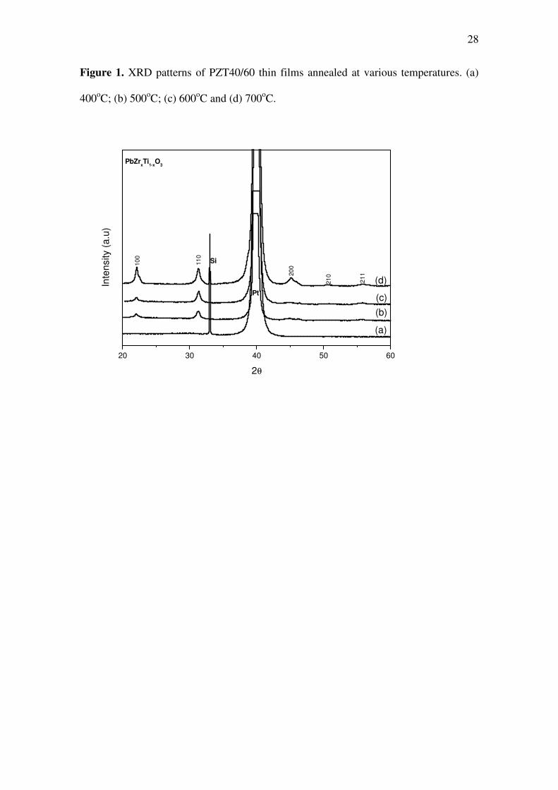
The crystalline nature of thin films was studied by XRD. Figure 1 shows XRD
patterns of PZT40 thin films on a Pt/Ti/SiO2/Si substrate annealed at different
temperatures for 2 hours. With increasing temperature, XRD peaks became sharper and
more intense which indicates the enhanced crystallinity of the thin films. Figure 1
illustrates that all diffraction peaks have a perovskite polycrystalline structure with no
evidence of preferential orientation or secondary phases except for the strong peak at 2θ
~39o which belongs to Pt substrates. Figure 1 also reveals that PZT thin films annealed
at 700oC exhibit lattice parameters of 0.401 nm (a-axis) and 0.414 nm (c-axis).
Moreover, the lattice parameter was almost unchanged above 600oC which indicates
that these PZT40 thin films have good crystallinity within this treatment temperature
range. In addition, these values are comparable with reported literature values for the
same composition.
Figure 2 shows FT-IR reflectance spectra of PZT40 thin films annealed at
different temperatures. For the polymeric precursor of a PZT40 thin film annealed at
150oC for 1 hour in air (see Figure 2a), undecomposed organic ligands are still present
in the thin film. Vibrations around 1750 cm-1 and at 1400 cm-1 are also observed which
can be related to the C = O stretching mode for the ester (R−COO−R). Vibrations at
1600 cm-1 and 1390 cm-1 are related to a COO- stretching mode for a bidentate complex.
At 400oC the spectrum displays a very broad absorption band of the BO6 stretching

10
mode, at 900 −600 cm-1 which suggests the formation of a solid oxide network disorder.
In addition, at 400oC, the bands associated with undecomposed organic ligands
completely disappear. With a temperature increase above 400oC, the broad absorption
band at 900 - 600cm-1 becomes sharper and narrower which suggests a structural
rearrangement of the BO6 and AO12 units resulting in perovskite phase formation as
verified by an increase in absorption band intensities at 690 cm-1 and 428 cm-1,
respectively.
The suitability of Raman spectroscopy has been proven for the investigation of
very complex systems such as ferroelectric solid solutions. In particular, Deluca et al.46
examined several PZT compositions in the proximity of the MPB by Raman
spectroscopy. Micro-Raman spectra measured at room temperature after thin films were
annealed at different temperatures are depicted in Figure 3. In agreement with XRD and
FT-IR analyses, PZT40 thin films show an amorphous structure which maintains the
disorder nature of AO6 and BO12 units after drying at 400oC; a broad shoulder is
observed at 773 nm. In addition, with increasing temperature, Raman spectra gradually
changed when Raman modes became active and stronger which is an indication of the
development of an ordered structure of the AO6 and BO12 units. This result points out
that the amorphous phase was gradually transformed to a tetragonal crystalline
perovskite phase as corroborated by XRD and FT-IR analysis.
Therefore, as discussed above, A1(1TO), E(2TO), B1+E, A1(
2TO), E(2LO) +
A(2LO), E(3TO), A1(3TO) and E(3LO) + A1(
3LO) phonon modes in the Raman spectra
provide unambiguous confirmation of the ferroelectric phase of PZT40 thin films
obtained by the chemical solution deposition method which corresponds to the
tetragonal structure. Figure 4 shows XRD patterns for a 100 nm thick PZT40 thin film
on a (h00) LaAlO3 substrate which used to analyze optical properties. Only reflections

11
from the (h00) planes of PZT40 thin films annealed at 700oC and LaAlO3 substrates
were observed which indicates that thin films were grown epitaxially on the LaAlO3
(100) transparent substrate into the perovskite single phase; no peaks with a pyrochlore
phase or a deleterious phase were found. Therefore, thin films are highly (h00) oriented
because the matching of lattice parameters between the a-axis of the LaAlO3 substrate
and PZT40 thin films is 4.5%. This result verifies that it is possible to obtain epitaxial
growth.
Figure 5 shows transmission spectra for 80 nm thick PZT40 thin films annealed
at 700oC for 2 hours recorded in the wavelength range of 200-1000 nm on a (100)
LaAlO3 substrate. The PZT40 thin film deposited on a (100) LaAlO3 substrate was
highly transparent in the visible region. The optical band gap of the PZT40 thin film
was determined in the high absorption region by using the Tauc relation described as
(αhν)m = A(hν - Eg) (1)
where m is a value which characterizes different types of transition (m = 2, 1/2, 2/3 or
1/3 for allowed direct, allowed indirect, forbidden direct and forbidden indirect
electronic transitions, respectively), hν is the photon energy, A a constant and Eg is the
optical band gap value.47-50 Thus, the dependence of (αhν)m versus incident photon
energy (hν) yields the Tauc optical band gap (Eg) value. As depicted in the inset of
Figure 5, the relationship between (αhν)2 and (αhν)1/2 plotted against hν varies linearly
in the high energy region of the absorption edge.
Based on the above process, Eg values were obtained by extrapolating the linear
portion of the plot relating (αhν)2 and (αhν)1/2 vs. hν to (αhν)2 = 0 and (αhν)1/2 = 0 and
considering the direct and indirect nature of the transition process to be ~4.03 and ~3.10
eV, respectively. Our calculated band gap value is greater than the band gap value
reported by Moret et al.30 which was determined by ellipsometry for epitaxial PbZxTi1-

12
xO3 thin films prepared by metal-organic chemical vapor deposition on a SrTiO3
substrate.
Puustinen et al.51 showed that as the thickness of PNZT (PbNx(ZyTi1-y)1-xO3) thin
films deposited on MgO (100) by pulsed laser deposition decreases from 300 to 150 nm,
the band gap values were 4.26 and 4.28 eV, respectively, and assumed direct band-to-
band transition. Pintilie et al.52 reported a value of 3.85 eV for a band gap of PZT92/8
thin films deposited by the sol-gel method on single crystal MgO(100) substrates.
Currently, spectroscopy ellipsometry is the optical technique most often utilized to
study optical properties of thin films.53-57 Recently, Suchaneck et al.55 investigated
optical properties of PZT thin films prepared by multi-target reactive sputter deposition
by ellipsometry spectra. The optical band gap for thin films was calculated using the
Tauc relationship by considering direct band gap transition. The results obtained by
ellipsometry revealed that, independent of the Zr/Ti ratio, band gap energies remain
nearly the same for all samples; phonon energy values of ,Eg 4.04 and ca. 3.99 eV
were obtained. However, researchers have assumed that the PZT exhibits a direct band
gap independent of the Zr content.20, 51, 56-59 To obtain optical properties, Lee et al.
determined band gap values for bulk PZT as a function of a Zr composition performed
within a local density approximation using the VASP package which shows a direct
band gap at the X point.38
This result suggests that experimental parameters (i.e, processes, temperature,
atmosphere, thickness and substrate) in the preparation of PbZrxTi1-xO3 thin films are
crucial in determining optical properties of these thin films. Consequently, different
band gap results for PZT thin films are expected for the same composition.
Dielectric and ferroelectric properties were determined for PZT thin films with a
thickness of ~250 nm which were annealed at 700oC on a Pt/Ti/SiO2/Si substrate

13
measured at room temperature. The room temperature dielectric constant and loss
tangent of PZT thin films as a function of measured frequency is recorded in Figure 6.
At frequencies range from 102 to 106 Hz, both the dielectric constant and the loss
tangent do not show noticeable changes with frequencies. These results suggest a good
degree of composition homogeneity, thickness uniformity and, more importantly, a
small concentration of space charges between electrode/thin film bottom and top PZT/Pt
and Au/PZT interfaces, respectively. PZT thin films have a dielectric constant and a loss
tangent of about 579 and 0.014, respectively, at 100 KHz.
Figure 7 demonstrates the bias dependence of the dielectric constant of the
Au/PZT/Pt capacitor at a frequency of 100 KHz at room temperature. The bias voltage
was swept quasistatically for each rising and falling bias cycle. The dielectric constant
exhibited a large variation with the bias. A hysteresis loop was observed when the
applied voltage was swept between positive and negative voltages. Therefore, the
butterfly shape indicates that the films reflected ferroelectric behavior at room
temperature.
The polarization-bias hysteresis curves of an Au/PZT/Pt capacitor where the
PZT layer has an average thickness of ~ 250 nm for various applied biases are shown in
Figure 8. When the applied bias is increased to higher values, a marked increased in Pr
values occurs, and shaped loops are obtained for PZT thin films which reflects good
ferroelectric properties. The measured remanent polarization (Pr) value ~ 23µC/cm2
derived from PZT thin films was obtained by a chemical solution deposition. In
addition, this observed value for Pr is comparable to values reported in the literature for
PZT thin films with approximately the same Zr/Ti ratio and Pt/Ti/SiO2/Si substrate.29, 60-
64 Jegatheesan et al.65 reported similar results for PZT thin films with a remanent
polarization of ~ 19µC/cm2 and a dielectric constant of ~ 450 at 1000 KHz. Zubko et al.

14
reported a remanent polarization of ~ 23µC/cm2 for PbZr0.40Ti0.60O3 thin film capacitors
using Pt bottom and Ir/IrO2 top electrodes.66
To further study the optical and electronic properties of PZT, first principle
calculations were conducted. Following the definition of Heifets et al.,67 the cleavage
energy ( usE ), the relaxation energy ( relE ) and the surface energy ( )i(Es ) for PT-TiO2,
PT-PbO, PZT-TiO2 and PZT-PbO have been calculated. This procedure had been used
in previous studies.68
usE has been calculated as:
( ) ( )[ ]bulk
uslab
uslab
us EXEPbOE
4
1E −+= (1)
where X is TiO2 or ZrO2 and usE represents unrelaxed PbO or TiO2 or ZrO2 terminated
slab energies. bulkE is the energy of a supercell constituted by five PbTiO3 units where
two Ti atoms are replaced by Zr atoms, n is the number of atomic layers, and a factor ¼
comes from the fact that we create four surfaces upon cleavage procedure. Erel for each
PbO, TiO2 and ZrO2, have been calculated as:
( ) ( ) ( )[ ]iEiE2
1iE
uslabslabrel
−= (2)
where ( )iEslab
is the slab energy after relaxation, and i is PbO or TiO2 or ZrO2
termination. The last one, ( )iEs , is the sum of the cleavage and relaxation energies:
( ) ( ) ( )iEiEiErel
uss += (3)
Table 1 shows these energies as a function of surface termination. A
comparison of the PT and PZT system shows a compensation of usE values (higher in
PZT than PT) with relE values (lower in PZT than PT) and similar surface energy

15
values. Table 1 also shows collected values for two more stable PZT system models.
The possibility of replacing Zr atoms by Ti atoms in the third and seventh layers of the
nine-layer TiO2 terminated slab was studied which resulted in small favored
combinations for PZT- PbO slabs.
The calculated direct and indirect optical gap values for PT and PZT systems are
summarized in Table 2. From an analysis of the band structure of TiO2 and PbO
terminated surfaces to the PT, there is a direct band gap energy of 3.84 eV for the PT-
TiO2 slab with the maximum energy for VB and the minimum energy for CB located at
the Γ point. However, the PT – PbO slab has an indirect band gap energy of 3.98 eV
between the points X - M. The top of the upper VB for the two possibilities of PZT
40/60, PbO(4th/8th) and PbO(2nd/10th) is located at the X point, and the bottom of the
lowest CB is located at the M point with indirect gaps of 3.67 eV and 3.45 eV,
respectively. The top of the upper VB for the PZT40/60 in the ZrO2 terminated surface
is located at the X point, and the bottom of the CB is located at the Γ point which yields
an indirect gap value of 3.63 eV.
An analysis of the results shows that in the PZT40/60 system, gap values are
smaller than gap values in the pure system (PT) for both terminations which can be
associated with the substitution Ti by Zr (see Figure 10). This change increases the Zr –
O bond distance and decreases the Ti – O bond distance with respect to previous and
subsequent layers (see Table 3). Therefore, this behavior can be assigned to a symmetry
breaking process of TiO6/ZrO6 octahedron clusters for both terminations.
Figures 11a and 11b depict the calculated total and projected densities of state on
atoms and orbitals of PT for PbO and TiO2 terminations. For both surfaces, the valence
bands are composed of 2p orbitals of O atoms but with a minor 2px contribution in TiO2
terminations. The first conduction band for both terminations shows many differences.

16
The PbO-terminated slab is derived mostly from 3dxz of the Ti atom. On the other hand,
in a TiO2 terminated slab, the conduction band with a broadened aspect has a mainly Ti
3dxz and 3dyz character with a minor contribution from 2zd3 orbitals.
Electronic properties of perfect cubic and defective (oxygen vacancy) PT and PZ
perovskites have been especially revised by Piskunov et al 69-72 at hybrid B3PW DFT
level. New energy levels located in the band gap due to F centers are compared in both
bulk and surface PT and PZ systems. In our case the exploration of the total and
projected DOS for the PZT40/60 system generates important differences with regard to
the PT system which is more relevant in the two types of PbO terminations PbO(4th/8th)
and PbO(2nd/10th) surfaces studied. In the PbO(4th/8th) slab, the principal component of
the top of the VB consists mainly of the O 2px orbital. The CB is mainly composed of
3dxz and 3dxy AO of Ti atoms and 6p AO of Pb atoms (see Figure 12a). Figure 12b
shows the projected DOS for PZT-ZrO2. An analysis of the principal AO component of
the top of the VB consists mainly of O 2px states as in PbO(4th/8th) termination. The CB
is composed mainly of Ti 3dxz orbitals which dominate the Ti 3dyz and 6p of Pb atoms.
However, in the PbO(2nd/10th) termination, the VB is composed of 2p orbitals of O
atoms, and the CB consists mainly Ti 3dxz and 6px and 6pz contributions of Pb atoms
(see Figure 13).
Thus, although the Zr AOs do not contribute directly to the gap energy range, O,
Ti, and Pb AOs are influenced by the Zr substitution. This result shows that adding Zr
atoms to the PT system decreases the overlapping between O 2p and Ti 3d orbitals. It is
apparent that contributions of the O 2p and Ti 3d states into the valence band (and the
conduction band) of PZT40/60 facets depend on the position of these atoms in the
corresponding surfaces.

17
VI. Conclusions
A joint experimental and theoretical study has been devoted to understanding the
structural, optical and electronic properties of PZT thin films. PZT40/60 thin films have
been successfully grown on Pt/Ti/SiO2/Si and LaAlO3 (100) substrates using the
chemical solution deposition method. To better understand the optical experimental
results, the electronic band structure of the PbTiO3 (PT) system and tetragonal
PbZr0.40Ti0.60O3 (PZT40/60) was calculated by first principle calculations. In addition,
structural and electronic properties of the PbO and ZrO2 terminated (100) surface of
tetragonal PZT40/60 were calculated. The main conclusions can be summarized as
follows: i) XRD analysis reveals that thin films grew with high (100) orientations on
LaAlO3 (100) substrates while on Pt/Ti/SiO2/Si substrates the thin films had a
polycrystalline growth; ii) the tetragonal phase was confirmed by Raman analysis; iii)
thin films exhibit ferroelectric and dielectric properties with a remanent polarization of
23 µC/cm2, while the dielectric constant values and loss tangent values are 579 and
0.014 at 100 KHz, respectively; iv) the transmittance curve of PZT40/60 thin films on
LaAlO3 (100) substrates had an optical band gap of 4.03 and 3.10 eV for the direct and
indirect transition process, respectively; v) the PT system shows indirect and direct
optical band gaps of 3.84 and 3.98 eV for PT-PbO and PT-TiO2 terminations,
respectively; vi) the PZT40/60 system shows indirect optical band gaps of 3.63/3.45 and
3.67 eV for the PbO(4th/8th)/ PbO(2nd/10th) and ZrO2 terminations, respectively (these
theoretical values are in agreement with the trends of experimental data); vii) our
theoretical results indicate that the introduction of Zr in the Ti site causes a distortion in
the crystal lattice which changes Ti-O and Zr-O bond distances which can be associated
with a breaking symmetry process of the octahedral clusters, TiO6/ZrO6, as polyhedra
constituents of this material for both terminations and viii) an analysis of density of

18
states reveals that atomic orbitals of Zr atom do not contribute directly to the band gap
energy range. However, adding Zr atoms to the PT system decreases the overlapping
between O 2p and Ti 3d orbitals.
Acknowledgments
This work is supported by the Spanish MALTA-Consolider Ingenio 2010 Program
(Project CSD2007-00045), Bancaixa Foundation (P11B2009-08), Spanish-Brazilian
Program (PHB2009-0065-PC), Ciencia e Innovación for project CTQ2009-14541-C02,
Generalitat Valenciana for Prometeo/2009/053 project, and by the financial support of
the Brazilian research financing institutions: CAPES, CNPq and FAPESP. The authors
also acknowledge the Servei Informatica, Universitat Jaume I for generous allotment of
computer time.
References
1. M. Dawber, K. M. Rabe and J. F. Scott, Reviews of Modern Physics, 2005, 77,
1083-1130.
2. N. Setter, D. Damjanovic, L. Eng, G. Fox, S. Gevorgian, S. Hong, A. Kingon, H.
Kohlstedt, N. Y. Park, G. B. Stephenson, I. Stolitchnov, A. K. Taganstev, D. V.
Taylor, T. Yamada and S. Streiffer, Journal of Applied Physics, 2006, 100,
051606.
3. A. Brinkman, M. Huijben, M. Van Zalk, J. Huijben, U. Zeitler, J. C. Maan, W.
G. Van der Wiel, G. Rijnders, D. H. A. Blank and H. Hilgenkamp, Nature
Materials, 2007, 6, 493-496.

19
4. J. L. Maurice, C. Carretero, M. J. Casanove, K. Bouzehouane, S. Guyard, E.
Larquet and J. P. Contour, Physica Status Solidi a-Applications and Materials
Science, 2006, 203, 2209-2214.
5. J. B. Neaton and K. M. Rabe, Applied Physics Letters, 2003, 82, 1586-1588.
6. N. Izyumskaya, Y. Alivov, S. J. Cho, H. Morkoc, H. Lee and Y. S. Kang,
Critical Reviews in Solid State and Materials Sciences, 2007, 32, 111-202.
7. R. Kagimura and D. J. Singh, Physical Review B, 2008, 78, 174105.
8. B. Xu, X. Li, J. Sun and L. Yi, European Physical Journal B, 2008, 66, 483-
487.
9. F. C. Zhang, Z. Y. Zhang, W. H. Zhang, J. F. Yan and J. N. Yun, Acta Physico-
Chimica Sinica, 2009, 25, 61-66.
10. T. Shimada, S. Tomoda and T. Kitamura, Journal of Physics-Condensed Matter,
2010, 22, 355901.
11. C. H. Ahn, J. M. Triscone and J. Mannhart, Nature, 2003, 424, 1015-1018.
12. D. D. Fong, G. B. Stephenson, S. K. Streiffer, J. A. Eastman, O. Auciello, P. H.
Fuoss and C. Thompson, Science, 2004, 304, 1650-1653.
13. H. Kumigashira, D. Kobayashi, R. Hashimoto, A. Chikamatsu, M. Oshima, N.
Nakagawa, T. Ohnishi, M. Lippmaa, H. Wadati, A. Fujimori, K. Ono, M.
Kawasaki and H. Koinuma, Applied Physics Letters, 2004, 84, 5353-5355.
14. A. Ohtomo, D. A. Muller, J. L. Grazul and H. Y. Hwang, Nature, 2002, 419,
378-380.
15. S. Okamoto and A. J. Millis, Nature, 2004, 428, 630-633.
16. E. Cross, Nature, 2004, 432, 24-25.
17. B. Noheda and D. E. Cox, Phase Transitions, 2006, 79, 5-20.

20
18. F. Chen, J. R. Cheng, S. W. Yu and Z. Y. Meng, Journal of Materials Science-
Materials in Electronics, 2010, 21, 514-518.
19. J. S. Cross, S. H. Kim, S. Wada and A. Chatterjee, Science and Technology of
Advanced Materials, 2010, 11, 044402.
20. E. Defay, T. Lacrevaz, T. T. Vo, V. Sbrugnera, C. Bermond, M. Aid and B.
Flechet, Applied Physics Letters, 2009, 94, 052901.
21. W. H. Duan and Z. R. Liu, Current Opinion in Solid State & Materials Science,
2006, 10, 40-51.
22. J. Frantti, Journal of Physical Chemistry B, 2008, 112, 6521-6535.
23. J. Frantti, Fujioka, Y., Zhang, J., Vogel, S. C., Wang, Y., Zhao, Y., Nieminen,
R. M., Journal of Physical Chemistry B, 2009, 113, 7967-7972.
24. J. F. Scott and C. A. Paz de Araujo, Science, 1989, 246, 1400-1405.
25. F. Cordero, F. Craciun and C. Galassi, Journal of Physics and Chemistry of
Solids, 2008, 69, 2172-2176.
26. J. Rouquette, J. Haines, G. Fraysse, A. Al-Zein, V. Bornand, M. Pintard, P.
Papet, S. Hull and F. A. Gorelli, Inorganic Chemistry, 2008, 47, 9898-9904.
27. Y. Cao, G. Sheng, J. X. Zhang, S. Choudhury, Y. L. Li, C. A. Randall and L. Q.
Chen, Applied Physics Letters, 2010, 97, 252904.
28. F. M. Pontes, M. S. Galhiane, L. S. Santos, A. Gavino, L. A. Petit, D. S. L.
Pontes, E. Longo, A. J. Chiquito and C. E. F. Costa, Applied Physics a-
Materials Science & Processing, 2009, 95, 693-698.
29. T. Zhang, G. J. Hu, H. J. Bu, J. Wu, J. H. Chu and N. Dai, Journal of Applied
Physics, 2010, 107, 084103.
30. M. P. Moret, M. A. C. Devillers, K. Worhoff and P. K. Larsen, Journal of
Applied Physics, 2002, 92, 468-474.

21
31. B. Noheda, J. A. Gonzalo, L. E. Cross, R. Guo, S. E. Park, D. E. Cox and G.
Shirane, Physical Review B, 2000, 61, 8687-8695.
32. I. Grinberg, V. R. Cooper and A. M. Rappe, Physical Review B, 2004, 69,
144118.
33. I. Grinberg and A. M. Rappe, Phase Transitions, 2007, 80, 351-368.
34. J. Hlinka, Ondrejkovic, P., Kempa, M., Borissenko, E., Krisch, M., Long, X.,
Ye, Z. -G., Physical Review B, 2011, 83, 140101.
35. Z. Zhang, L. Lu, C. Shu, P. Wu and W. Song, Journal of Applied Physics, 2007,
102, 074119.
36. K. Miura and M. Tanaka, Japanese Journal of Applied Physics Part 1-Regular
Papers Short Notes & Review Papers, 1996, 35, 2719-2725.
37. I. Grinberg, V. R. Cooper and A. M. Rappe, Nature, 2002, 419, 909-911.
38. H. Lee, Y. S. Kang, S. J. Cho, B. Xiao, H. Morkoc, T. D. Kang, G. S. Lee, J. Li,
S. H. Wei, P. G. Snyder and J. T. Evans, Journal of Applied Physics, 2005, 98,
094108.
39. J. A. Rodriguez, A. Etxeberria, L. Gonzalez and A. Maiti, Journal of Chemical
Physics, 2002, 117, 2699-2709.
40. Z. Zhang, P. Wu, K. P. Ong, L. Lu and C. Shu, Physical Review B, 2007, 76,
125102.
41. C. Laulhe, A. Pasturel, F. Hippert and J. Kreisel, Physical Review B, 2010, 82,
132102.
42. I. Levin, E. Cockayne, V. Krayzman, J. C. Woicik, S. Lee and C. A. Randall,
Physical Review B, 2011, 83, 094122.

22
43. F. M. Pontes, E. R. Leite, M. S. J. Nunes, D. S. L. Pontes, E. Longo, R.
Magnani, P. S. Pizani and J. A. Varela, Journal of the European Ceramic
Society, 2004, 24, 2969-2976.
44. A. D. Becke, Journal of Chemical Physics, 1993, 98, 5648-5652.
45. C. T. Lee, W. T. Yang and R. G. Parr, Physical Review B, 1988, 37, 785-789.
46. H. F. M. Deluca, N. Tonari, C. Capiani, N. Hasuike, K. Kisoda, C. Galassid and
H. Harima, J. Raman Spectrsocopy, 2011, 42, 488.
47. M. Bousquet, J. R. Duclere, E. Orhan, A. Boulle, C. Bachelet and C.
Champeaux, Journal of Applied Physics, 2010, 107, 104107.
48. Q. Z. Liu, J. M. Dai, Z. L. Liu, X. B. Zhang, G. P. Zhu and G. H. Ding, Journal
of Physics D-Applied Physics, 2010, 43, 455401.
49. F. M. Pontes, E. R. Leite, D. S. L. Pontes, E. Longo, E. M. S. Santos, S.
Mergulhao, P. S. Pizani, F. Lanciotti, T. M. Boschi and J. A. Varela, Journal of
Applied Physics, 2002, 91, 5972-5978.
50. F. M. Pontes, D. S. L. Pontes, E. R. Leite, E. Longo, E. M. S. Santos, S.
Mergulhao and J. A. Varela, Journal of Sol-Gel Science and Technology, 2003,
27, 137-147.
51. J. Puustinen, J. Lappalainen and V. Lantto, Thin Solid Films, 2008, 516, 6458-
6463.
52. L. Pintilie, I. Boerasu, M. Gomes and M. Pereira, Thin Solid Films, 2004, 458,
114-120.
53. I. Aulika, V. Zauls, K. Kundzins, M. Kundzins and S. Katholy, Journal of
Optoelectronics and Advanced Materials, 2003, 5, 755-761.

23
54. D. Chvostova, L. Pajasova and V. Zelezny, in Physica Status Solidi C - Current
Topics in Solid State Physics, Vol 5, No 5, edited by H. Arwin, U. Beck and M.
Schubert (2008), Vol. 5, pp. 1362-1365.
55. G. Suchaneck, D. Chvostova, J. Kousal, V. Zelezny, A. Lynnyk, L. Jastrabik, G.
Gerlach and A. Dejneka, Thin Solid Films, 2011, 519, 2885-2888.
56. X. G. Tang, Q. X. Liu, L. L. Jiang and A. L. Ding, Materials Chemistry and
Physics, 2007, 103, 329-333.
57. S. H. Yang, Y. L. Zhang and D. Mo, Materials Science and Engineering B-Solid
State Materials for Advanced Technology, 2006, 127, 117-122.
58. S. K. Pandey, A. R. James, R. Raman, S. N. Chatterjee, A. Goyal, C. Prakash
and T. C. Goel, Physica B-Condensed Matter, 2005, 369, 135-142.
59. M. M. Zhu, Z. H. Du and J. Ma, Journal of Applied Physics, 2010, 108, 113119.
60. R. Bouregba, N. Sama, C. Soyer, G. Poullain and D. Remiens, Journal of
Applied Physics, 2010, 107, 104102.
61. J. W. Li, H. Kameda, B. N. Q. Trinh, T. Miyasako, P. T. Tue, E. Tokumitsu, T.
Mitani and T. Shimoda, Applied Physics Letters, 2010, 97, 102905.
62. B. T. Liu, J. W. Zhao, X. H. Li, Y. Zhou, F. Bian, X. Y. Wang, Q. X. Zhao, Y.
L. Wang, Q. L. Guo, L. X. Wang and X. Y. Zhang, Applied Physics Letters,
2010, 96, 252904.
63. N. Sama, R. Herdier, D. Jenkins, C. Soyer, D. Remiens, M. Detalle and R.
Bouregba, Journal of Crystal Growth, 2008, 310, 3299-3302.
64. X. Zhao, J. Y. Dai, X. G. Tang, J. Wang, H. L. W. Chan and C. L. Choy,
Applied Physics a-Materials Science & Processing, 2005, 81, 997-1000.
65. P. Jegatheesan, H. K. Yadav, V. Gupta and N. V. Giridharan, Materials Letters,
2011, 65, 901-904.

24
66. P. Zubko, D. J. Jung and J. F. Scott, Journal of Applied Physics, 2006, 100,
114113.
67. E. Heifets, R. I. Eglitis, E. A. Kotomin, J. Maier and G. Borstel, Physical Review
B, 2001, 64, 235417.
68. S. de Lazaro, E. Longo, J. R. Sambrano and A. Beltran, Surface Science, 2004,
552, 149-159.
69. S. Piskunov, E. Heifets, R. I. Eglitis and G. Borstel, Computational Materials
Science, 2004, 29, 165-178.
70. S. Piskunov, A. Gopeyenko, E. A. Kotomin, Y. F. Zhukovskii and D. E. Ellis,
Computational Materials Science, 2007, 41, 195-201.
71. E. A. Kotomin, S. Piskunov, Y. F. Zhukovskii, R. I. Eglitis, A. Gopejenko and
D. E. Ellis, Physical Chemistry Chemical Physics, 2008, 10, 4258-4263.
72. Y. F. Zhukovskii, E. A. Kotomin, S. Piskunov and D. E. Ellis, Solid State
Communications, 2009, 149, 1359-1362.

25
Table 1. usE , relE
and ( )iEs for PT and PZT40/60 as a function of termination. In
parenthesis is located the layer in which Ti atom is substituted by Zr.
Systems Termination usE relE ( )iEs (eV/cell)
PbTiO3 PbO 0.153
-0.036 3.184
TiO2 -0.036 3.184
PZT40/60 PbO (4th/8th) 0.200
-0.092 2.936
ZrO2 (1st/9th) -0.075 3.410
PbO (2nd/10th) 0.202
-0.087 3.136
ZrO2(1st/9th) -0.075 3.473

26
Table 2. Calculated optical gap (eV) for the PT-TiO2, PT-PbO, PZT40/60-ZrO2 and
PZT40/60-PbO terminations.
PT-TiO2 PT-PbO PZT-ZrO2 PZT-PbO
(4th/8th)
PZT-PbO
(2nd/10th)
Direct Γ 3.84 4.04 4.03 4.32
Indirect X-Γ - 3.98 - - -
X-M - - - 3.63 3.45
X’-Γ - - 3.67 - -

27
Table 3. Displacements of the atoms ∆Z (Å), of uppermost two layers from their perfect
lattice positions in PZT 40/60 surface. c refers to the central layer.
PZT-ZrO2 PZT-PbO(4th/8th) PZT-PbO(2nd/10th)
∆Z (Å) layer ∆Z (Å) layer ∆Z (Å) layer
0.2528 1-2 0.0121 1-2 0.2306 1-2
-0.0489 2-3 -0.0288 2-3 0.1377 2-3
0.0326 3-4 0.2112 3-4 -0.0156 3-4
-0.0010 4-c 0.1585 4-5 0.0031 4-5
-0.0168 5-c -0.0011 5-c
28
Figure 1. XRD patterns of PZT40/60 thin films annealed at various temperatures. (a)
400oC; (b) 500oC; (c) 600oC and (d) 700oC.
20 30 40 50 60
PbZrxTi
1-xO
3
21
0
21
120
0
11
0
10
0
Pt
Si
(d)
(c)
(b)
(a)
Inte
nsity (
a.u
)
2θ

29
Figure 2. FT-IR spectra of PZT40/60 thin films on Pt/Ti/SiO2/Si substrate annealed at
various temperatures. (a) as-prepared thin films; (b) 400oC; (c) 500oC; (d) 600oC, and
(d) 700oC.
400 600 800 1000 1200 1400 1600 1800 2000 2200
(e)
(d)
(c)
(b)
(a)
PbZrxTi
1-xO
3
Inte
nsity (
a.u
.)
Wavenumber (cm-1)

30
Figure 3. Raman spectra at room temperature for PZT40/60 thin films annealed at
varius temperatures. (a) 400oC; (b) 500oC; (c) 600oC and (d) 700oC.
100 200 300 400 500 600 700 800 900
E(3
LO
)+A
1(3
LO
)
A1(3
TO
)
E(3
TO
)
E(2
LO
)+A
(2L
O)
A1(2
TO
)B1+
E
E(2
TO
)
(d)
(c)
(b)
(a)
PbZrxTi
1-xO
3
Inte
nsity (
a.u
.)
Raman shift (cm-1)

31
Figure 4. X-ray diffraction patterns for the PZT40/60 thin films deposited on LaAlO3
(100) substrate.
20 25 30 35 40 45 50 55 60
2001
00
**
# #
# LaAlO3(100)
* PbZrxTi
1-xO
3
Inte
nsity (
a.u
.)
2θ

32
Figure 5. Optical transmission spectra measured of PZT40/60 thin films on
LaAlO3(100) substrate. The inset shows the plots of (hνα)2 versus hν and (hνα)
1/2
versus hν.

33
Figure 6. The variation of dielectric constant and loss tangent for PZT40/60 thin films
deposited on Pt/Ti/SiO2/Si substrates and annealed at 700oC.
100 1k 10k 100k 1M 10M
0
100
200
300
400
500
600
700
800
Loss T
an
gen
t (t
an
δ)
Die
lectr
ic c
onsta
nt (ε
)
Frequency (Hz)
0.0
0.1
0.2
0.3
0.4
0.5

34
Figure 7. The dependence of the dielectric constant of the PZT40/60 thin films
annealed at 700oC on the bias applied at 100 kHz.
-10 -8 -6 -4 -2 0 2 4 6 8 10
400
450
500
550
600
650
700
750
Die
lectr
ic C
on
sta
nt (ε
)
Bias (Volts)

35
Figure 8. Hysteresis loops for the PZT40/60 thin films measured at different bias
applied. (a) 6V; (b) 8V, and (c) 12V.
-15 -10 -5 0 5 10 15
-50
-40
-30
-20
-10
0
10
20
30
40
50
(c)
(b)
(a)
Po
lari
za
tio
n (
µC
/cm
2)
Bias (Volts)

36
Figure 9. Side view of PbTiO3 slab system, (a) TiO2 terminated nine layers slab and (b)
PbO termination eleven layers. O atoms are depicted in red and Ti atoms in blue and Pb
atoms in grey.
(b)(a)
PbO
TiO2
PbO
TiO2
PbO
TiO2
PbO
TiO2
PbO
TiO2
PbO

37
Figure 10. Side view of PZT4060 slab system, (a) ZrO2 terminated nine layers slab (b)
PbO(4th/8th) termination eleven layers and (c) PbO(2nd/10th) termination eleven layers. O
atoms are depicted in red, Ti atoms in blue, Pb atoms in grey and Zr atoms in brown.
Displacements ∆Z between layers are also marked.
∆Z12
∆Z23
∆Z34
∆Z4c
(b)(a) (c)
∆Z12
∆Z23
∆Z34
∆Z45
∆Z5c

38
Figure 11. Calculated total and projected DOS of the PbTiO3 system. (a) PbO
terminated and (b) TiO2 terminated.
a) b)
DO
S
O
s
px
py
pz
DO
S T
i
dxz
dyz
dxy
DO
S
Pb
s
py
pz
Ti
Pb
O
TOTAL
-8 -7 -6 -5 -4 -3 -2 -1 0
Energy (eV)
Pb
Ti
O
TOTAL
DO
S O
s
px
py
pz
DO
S T
i dz2
dxz
dyz
DO
S P
b s
px
py
pz
Ti
O
TOTAL
Pb s
px
py
pz
-8 -7 -6 -5 -4 -3 -2 -1 0
Energy (eV)
Pb
O Ti
TOTAL

39
Figure 12. Calculated total and projected DOS of the PZT40/60 system. (a) PbO
(4th/8th) terminated and (b) ZrO2 terminated.
a) b)
-6 -5 -4 -3 -2 -1 0 1
Pb
Zr
O
Ti
TOTAL
-6 -5 -4 -3 -2 -1 0 1
Pb
Zr
O
Ti
TOTAL
-6 -5 -4 -3 -2 -1 0 1
Ti
dxy
dxz
dy2
dz2
dx2-y
2
-6 -5 -4 -3 -2 -1 0 1
Ti
dxy
dxz
dy2
dz2
dx2-y
2
s
px
py
pz
s
px
py
pz
dz2
dxz
dyz
s
px
py
pz
Pb
O
TOTAL
-7 -6 -5 -4 -3 -2 -1 0
TOTAL
Energy (eV)
Pb
Zr
O
Ti
TOTAL
-7 -6 -5 -4 -3 -2 -1 0
TOTAL
Energy (eV)
Pb
Zr
O
Ti
TOTAL
s
px
py
pz
dxz
dyz
dx2
s
px
py
pz
Ti
Pb
O
dxz
dyz
dxy
Energy (eV)
Ti

40
Figure 13. Calculated total and projected DOS of the PZT40/60 system considering
PbO(2nd/10th) termination.
-8 -7 -6 -5 -4 -3 -2 -1 0
s
px
py
pz
-8 -7 -6 -5 -4 -3 -2 -1 0
dxz
dyz
dxy
s
px
py
pz
-8 -7 -6 -5 -4 -3 -2 -1 0
Energy (eV)
Pb
Zr
O
Ti
TOTAL
Ti
Pb
O
TOTAL