Synthesis of vertically aligned ultra-long ZnO nanowires ... · PDF fileSynthesis of...
7
Synthesis of vertically aligned ultra-long ZnO nanowires on heterogeneous substrates with catalyst at the root This article has been downloaded from IOPscience. Please scroll down to see the full text article. 2012 Nanotechnology 23 055604 (http://iopscience.iop.org/0957-4484/23/5/055604) Download details: IP Address: 130.207.50.37 The article was downloaded on 24/01/2012 at 15:57 Please note that terms and conditions apply. View the table of contents for this issue, or go to the journal homepage for more Home Search Collections Journals About Contact us My IOPscience
Transcript of Synthesis of vertically aligned ultra-long ZnO nanowires ... · PDF fileSynthesis of...

Synthesis of vertically aligned ultra-long ZnO nanowires on heterogeneous substrates with
catalyst at the root
This article has been downloaded from IOPscience. Please scroll down to see the full text article.
2012 Nanotechnology 23 055604
(http://iopscience.iop.org/0957-4484/23/5/055604)
Download details:
IP Address: 130.207.50.37
The article was downloaded on 24/01/2012 at 15:57
Please note that terms and conditions apply.
View the table of contents for this issue, or go to the journal homepage for more
Home Search Collections Journals About Contact us My IOPscience

IOP PUBLISHING NANOTECHNOLOGY
Nanotechnology 23 (2012) 055604 (6pp) doi:10.1088/0957-4484/23/5/055604
Synthesis of vertically aligned ultra-longZnO nanowires on heterogeneoussubstrates with catalyst at the root
Guang Zhu1, Yusheng Zhou1, Sihong Wang1, Rusen Yang2, Yong Ding1,Xue Wang1,3, Yoshio Bando4 and Zhong lin Wang1
1 School of Material Science and Engineering, Georgia Institute of Technology, Atlanta, GA 30332, USA2 Department of Mechanical Engineering, University of Minnesota, Minneapolis, MN 55455, USA3 Department of Applied Physics, Chongqing University, Chongqing 400044, People’s Republic of China4 World Premier International Center for Materials Nanoarchitectonics (MANA), National Institute forMaterials Science, Namiki1-1, Tsukuba, Ibaraki 305-004, Japan
E-mail: [email protected]
Received 24 October 2011, in final form 28 November 2011Published 11 January 2012Online at stacks.iop.org/Nano/23/055604
AbstractThe synthesis of ultra-long high-quality ZnO nanowires with uniform size and orientation onheterogeneous substrates is highly desirable, not only for investigating the fundamentalproperties of ZnO nanowires, but also for fabricating integrated functional nanodevices. Herewe present a novel and general technique for growing vertically aligned ultra-long ZnOnanowires on various substrates. More importantly, the metal catalyst is experimentallydetermined not at the tip ends of the nanowires but at the junction area between the nanowiresand the underlying substrate. Based on detailed analysis and control group results, we thenpropose a three-stage growth mechanism, in which vapor–liquid–solid growth and vapor–solidgrowth compete with each other to become dominant.
(Some figures may appear in colour only in the online journal)
1. Introduction
In the last decade, one-dimensional (1D) ZnO nanostructures,such as nanowires (NWs), nanobelts, and nanorods have beenreceiving considerable attention due to their unique propertiesfor electronic and optoelectronic applications [1–4]. A varietyof ZnO NW based devices have been demonstrated, includingfield effect transistors [5–7], UV lasers [8, 9], light emittingdiodes [10–12], solar cells [13–15], photodetectors [16–18],nanogenerators [19–21], and piezotronics [22, 23]. As thebasis for various applications, synthesis with control oversize, orientation, and density is of great significance andvery much desired. The main synthesis techniques includephysical vapor deposition [1, 5, 24, 25], chemical vapordeposition [26–29], pulsed layer deposition [30] and thewet chemical method [31–33]. For the widely employedvapor transport method, different growth mechanisms havebeen reported, including catalyst-assisted vapor–liquid–solid
(VLS) growth and catalyst-free vapor–solid (VS) growth. Onone hand, the VLS mechanism usually yields ZnO NWs withsize and orientation uniformity, but residual metal catalystparticles often stay at the tips of the NWs [34], which isvery detrimental to further device integration because theseparticles prevent intimate contact between the NWs andelectrode materials. Besides, as demonstrated by previousreports, the lengths of the ZnO NWs grown from the VLSmechanism are limited to only a few micrometers [26–28].On the other hand, methods with the VS mechanism cangrow ZnO NWs with lengths up to hundreds of micrometers,which nevertheless generally have rather poor alignment anduniformity [1, 35].
Here we report a uniquely modified and general techniqueof synthesizing ultra-long ZnO NWs with great verticalalignment on different substrates, with length and aspect ratioexceeding 130 µm and 500, respectively. More importantly,pre-deposited metal catalysts were experimentally confirmed
10957-4484/12/055604+06$33.00 c© 2012 IOP Publishing Ltd Printed in the UK & the USA

Nanotechnology 23 (2012) 055604 G Zhu et al
Figure 1. (a) Schematic illustration of the source material preparation and the horizontal furnace system for the synthesis of ultra-long ZnONW arrays. (b) Cross-sectional view of the synthesized ZnO NWs on the Si substrate. (c) 60◦ tilted view of the synthesized ZnO NWs onthe Si substrate. (d) Cross-sectional view of the synthesized ZnO NWs using conventional source materials without pretreatments.
at the roots instead of the tip ends of the NWs. Furthermore,a series of control experiments was conducted to investigatethe actual growth mechanism. Finally, a unique growthmodel was proposed, combining VLS and VS growth inthree consecutive stages. Our synthesis technique opens upthe path for fabricating various functional devices based onhigh-quality ZnO NW arrays.
2. Experimental section
In general, the limited length of NWs synthesized by thechemical vapor transport method is possibly due to therelatively low reactive vapor concentration in the synthesistube and thus the slow growth speed. To overcome thischallenge, two unique strategies were employed in ourwork. The first one involves pretreatment of the sourcematerials, as schematically illustrated in figure 1(a). Ratherthan using the conventionally used ZnO powder and graphitepowder, we used commercially available ZnO nanopowder(Sigma-Aldrich) and activated carbon powder (Alfa Aesar) assource materials. Respectively, amounts of 1 g were used asreceived. They were then dispersed in ethanol. The suspensionwas ultrasonicated for 30 min to ensure uniform dispersion.Then it was put in a hot oven for drying for another 30 min.After the ethanol had completely vaporized, the dried mixturewas then well ground and ready for use. The use of nano-sizedsource materials and the pretreatment measures are expectedto greatly increase the amount of reactive vapor released
during the growth. The second strategy was to modify theconventional synthesis configuration in which the sourcematerials and substrates are separately located at the centerand downstream side of the furnace tube, respectively. Asshown at the bottom of figure 1(a), the already preparedsource materials were transferred to an alumina boat. Siliconwafer substrates coated with gold thin film were horizontallymounted on top of the boat with the gold layer facing down.This non-conventional configuration is expected to greatlyincrease the local concentration of the reactive vapor at thegrowth site and the growth speed as a result [36]. The boatwas then placed at the center of the furnace tube. Silicon wafer(100) substrates were dipped in buffered oxide etching (BOE)solution for 10 s to strip off the native oxide layer, cut into1.8 cm× 1.8 cm pieces and then rinsed by acetone, methanol,and isopropyl alcohol, consecutively. A 2 nm gold catalystlayer was coated by e-beam evaporation with a deposition rateof 0.1 A s−1. During the growth, the temperature was rampedup to 960 ◦C at a rate of 60 ◦C min−1 with a constant flow ofcarrier gas (30 sccm of argon and 10 sccm of oxygen). Thereaction lasted for 30 min. After the reaction, the furnace wascooled down to ambient temperature for product collection.
The morphology of the synthesized ZnO nanowires wasexamined by an LEO 1530 SEM at 5 kV accelerating voltage.The XRD data were collected with Cu Kα radiation ona Panalytical X’Pert PRO Alpha-1. The TEM image of asingle ZnO nanowire was recorded on a Hitachi HF-2000with an accelerating voltage of 200 kV. The TEM images of
2
Nanotechnology 23 (2012) 055604 G Zhu et al
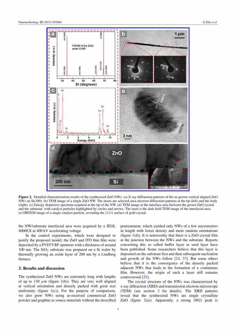
Figure 2. Detailed characterization results of the synthesized ZnO NWs. (a) X-ray diffraction patterns of the as-grown vertical aligned ZnONWs on Si(100). (b) TEM image of a single ZnO NW. The insets are selected-area electron diffraction patterns at the tip (left) and the body(right). (c) Energy dispersive spectrum acquired at the tip of the NW. (d) TEM image at the interface area between the grown ZnO crystaland the substrate, with catalyst particles highlighted by circles and arrows. The inset is the dark field TEM image of the interfacial area.(e) HRTEM image of a single catalyst particle, revealing the {111} surface of gold crystal.
the NW/substrate interfacial area were acquired by a JEOL4000EX at 400 kV accelerating voltage.
In the control experiments, which were designed tojustify the proposed model, the ZnO and ITO thin film weredeposited by a PVD75 RF sputterer with a thickness of around100 nm. The SiO2 substrate was prepared on a Si wafer bythermally growing an oxide layer of 200 nm by a Lindbergfurnace.
3. Results and discussion
The synthesized ZnO NWs are extremely long with lengthsof up to 130 µm (figure 1(b)). They are very well alignedat vertical orientation and densely packed with great sizeuniformity (figure 1(c)). For the purpose of comparison,we also grew NWs using as-received commercial ZnOpowder and graphite as source materials without the described
pretreatment, which yielded only NWs of a few micrometersin length with lower density and more random orientations(figure 1(d)). It is noteworthy that there is a ZnO crystal filmat the junction between the NWs and the substrate. Reportsconcerning this so called buffer layer or seed layer havebeen published. Some researchers believe that this layer isdeposited on the substrate first and then subsequent nucleationand growth of the NWs follow [24, 37]. But some othersbelieve that it is the convergence of the densely packedadjacent NWs that leads to the formation of a continuousfilm. However, the origin of such a layer still remainscontroversial [25].
The crystal structure of the NWs was characterized byx-ray diffraction (XRD) and transmission electron microscope(TEM) (see section 2 for details). The XRD patternsreveal that the synthesized NWs are single crystallineZnO (figure 2(a)). Apparently, a strong (002) peak is
3

Nanotechnology 23 (2012) 055604 G Zhu et al
Figure 3. (a) 60◦ tilted view of the synthesis result on a ZnO substrate, with no catalyst applied before growth. The inset is thecross-sectional view. (b) 60◦ tilted view of the synthesis result on an ITO substrate, with catalyst applied before growth. (c) 60◦ tilted viewof the synthesis result on a SiO2 substrate, with catalyst applied before growth. (d) Schematic illustration of the ZnO NW growth processvia a three-stage mechanism.
overwhelmingly predominant with other peaks almostnegligible, indicating uniform orientation as well as greatdensity of the NWs. A TEM image of a single NW(figure 2(b)) shows a typical diameter of 250 nm. Theselected-area electron diffraction (SAED) pattern provesagain the single crystalline nature of the NW and exhibits thegrowth along the [0001] direction (right inset of figure 2(b)).It is observed from the TEM image that the NW tip seems tobe free of any catalyst particle! The SAED pattern acquired atthe tip shows no patterns other than ZnO crystal (left inset offigure 2(b)). Besides, the EDS spectrum measured at the tipalso gives no trace of gold element (figure 2(c)), confirmingthat the gold catalysts are absent from the tip end.
Although the observation that catalyst-assisted growthproduces NWs with catalyst-free tip ends has beenreported [19, 20, 36, 38–40], very few successful attemptshave been made to determine the underlying reason. Someresearchers believe that the catalyst is doped into the NWas contamination [24], while some others suggest that itevaporates during the growth process [19, 20]. However,convincing experimental results are lacking. Here, weprepared extremely thin cross-sectional samples for TEMcharacterization. The TEM image targeting the NW/substrateinterfacial area reveals a very interesting phenomenon. Alayer of particles can be clearly spotted at the roots of theNWs, which is highlighted in figure 2(d). The dark field TEMimage (inset of figure 2(d)) reveals the continuous ZnO filmlying between the NWs and the substrate to be a texturedlayer, which is composed of adjacent crystal domains. Thehigh resolution transmission diffraction (HRTEM) image of a
single particle exhibits a set of lattice planes with a measureddistance of 2.35 A, corresponding to {111} of gold crystal.The decisive experimental evidence confirms that the metalcatalyst stays at the roots of the synthesized ZnO NWs.This phenomenon is a strong indication that the ZnO NWsynthesis using our technique is not simply governed by theVLS mechanism, which is consistent with a previous reportby Fan et al [38]. It is noticeable that the catalyst particles donot adhere closely to the underlying substrate and that theirrespective distances away from the substrate vary. As a result,they are expected to have negligible influence on the electrontransport behavior at the NW/substrate interface.
Such an unexpected discovery raises two importantquestions, i.e. how the metal catalyst ends up staying at theinterfacial area and what role it plays during the growthprocess. To shed light on the actual growth mechanism, aseries of control experiments was performed.
In the first group, no gold catalyst was pre-depositedon the substrate, while the other experimental parametersremained unchanged. As a result, NW growth was notobserved, which is a strong proof that the gold catalyst isindispensable for initializing the growth [36, 40].
In the second group, a sputtered ZnO film as a seedlayer was prepared on a bare Si substrate surface, andno catalyst was applied. The growth result is presented infigure 3(a). Vertically oriented ZnO NWs with a length oftens of micrometers were successfully synthesized, indicatingthat VS growth should be dominating if a seed layer isprovided [24, 25, 37].
4

Nanotechnology 23 (2012) 055604 G Zhu et al
In the third group, a ITO film was sputtered on a Sibare substrate surface, followed by coating a gold catalystlayer. Ultra-long ZnO NW arrays were synthesized withhigh quality, as shown in figure 3(b). Other substrates,such as thermally grown SiO2, yielded similar results(figure 3(c)). This is a strong indication that the growth is trulycatalyst-assisted. As long as the gold catalyst is provided, thegrowth can take place no matter what the underlying substrateis. In addition, this observation proves that our synthesistechnique is very general, and is applicable to other substratesbesides Si wafer. Therefore, various heterojunctions areexpected to be formed.
Based on our characterization analysis and controlgroups, we propose a three-stage growth model, asschematically illustrated in figure 3(d). During the growth, Znvapor is generated by carbon thermal reaction [26]
ZnO (s)+ C (s)←→ Zn (v)+ CO (v) (1)
followed by [28]
2Zn (v)+ O2 (v) = 2ZnO (v). (2)
Between the Zn vapor and ZnO vapor, which one wouldparticipate in the NW growth depends on the surface conditionof the substrate.
In the early stage of the growth, it is the Zn vaporthat can be easily dissolved into the gold particles to formliquid alloys. Upon supersaturation, it reacts with oxygen,precipitating out very thin ZnO textured seeds beneath thecatalyst particles [26]. Thus the first stage is purely dominatedby VLS growth.
Then the seeds provide nucleation and growth sites forZnO vapor [24, 38]. The abundant and continuous arrival ofZnO vapor makes very rapid VS growth possible [35], whichmay far exceed the VLS growth. Consequently, the catalystparticles will soon be submerged because of the VS growth,which can explain why the catalyst particles do not adhereto the undying substrate but are encapsulated by ZnO crystal.Therefore, in the second stage, although VLS growth does notcease, it is the VS growth that prevails.
In the last stage, the catalyst particles have been isolatedfrom the reagent vapor and do not play any role afterward.As a result, only the VS mechanism contributes to thefurther growth of ZnO NWs [24]. Therefore, based on ourmodel, the metal catalyst mainly plays two roles. First, itis crucial for initializing the growth by absorbing Zn vapor.Second, it precipitates ZnO texture seeds, which not onlyprovide templates for further growth but also guide the growthorientation, leading to alignment of the NWs.
4. Conclusions
In summary, we developed a uniquely modified and generaltechnique for synthesizing vertically aligned ultra-long ZnONWs on various substrates. The NWs have great density anduniformity, with length and aspect ratio exceeding 130 µmand 500, respectively. Catalyst particles were experimentallyproved to be at the NW/substrate interface area instead of thetip ends. A series of control experiments was performed to
understand the growth process. A three-stage growth modelwas then proposed. It involves a combination of VLS growthand VS growth, which compete with each other to becomedominant. Our technique opens up a path for fabricatingintegrated high-performance devices based on ZnO NWarrays.
Acknowledgments
This research was supported by DARPA (HR0011-09-C-0142, Program manager: Dr Daniel Wattendorf), BES DOE(DE-FG02-07ER46394), and MANA from NIMS Japan.
References
[1] Pan Z W, Dai Z R and Wang Z L 2001 Science 291 1947–9[2] Wang Z L 2009 Mater. Sci. Eng. R 64 33–71[3] Yang P, Yan H, Mao S, Russo R, Johnson J, Saykally R,
Morris N, Pham J, He R and Choi H J 2002 Adv. Funct.Mater. 12 323–31
[4] Wang Z L 2008 ACS Nano 2 1987–92[5] Wang W Z, Zeng B Q, Yang J, Poudel B, Huang J Y,
Naughton M J and Ren Z F 2006 Adv. Mater. 18 3275–8[6] Wang X D, Zhou J, Lao C S, Song J H, Xu N S and
Wang Z L 2006 Nano Lett. 6 2768–72[7] Wang X D, Zhou J, Lao C S, Song J H, Xu N S and
Wang Z L 2007 Adv. Mater. 19 1627–31[8] Huang M H, Mao S, Feick H, Yang H, Wu Y, Kind H,
Weber E, Russo R and Yang P 2001 Science 292 1897–9[9] Zou B, Liu R, Wang F, Pan A, Cao L and Wang Z L 2006
J. Phys. Chem. B 110 12865–73[10] Lim J H, Kang C K, Kim K K, Park I K, Kwang D K and
Park S J 2006 Adv. Mater. 18 2720–4[11] Zhang X M, Lu M Y, Zhang Y, Chen L J and Wang Z L 2009
Adv. Mater. 21 2767–70[12] Xu S et al 2010 Adv. Mater. 22 4749–53[13] Law M, Greene L E, Johnson J C, Saykally R and
Yang P 2005 Nature Mater. 4 455–9[14] Weintraub B, Wei Y and Wang Z L 2009 Angew. Chem. Int.
Ed. 48 1–6[15] Wei Y, Xu C, Xu S, Li C, Wu W and Wang Z L 2010 Nano
Lett. 10 2092–6[16] Kind H, Yang H, Messer B, Law M and Yang P 2002 Adv.
Mater. 14 158–66[17] Law J B K and Thong J T L 2006 Appl. Phys. Lett. 88 133114[18] Yang Q, Guo X, Wang W, Zhang Y, Xu S, Lien D H and
Wang Z L 2010 ACS Nano 4 6285–91[19] Wang Z L and Song J H 2006 Science 312 242–6[20] Wang X D, Song J H and Wang Z L 2007 Science 316 102–5[21] Yang R, Qin Y, Dai L and Wang Z L 2008 Nature
Nanotechnol. 4 34–9[22] Wang Z L 2010 Nano Today 5 540–52[23] Wang Z L, Yang R, Zhou J, Qin Y, Xu C, Hu Y and
Xu S 2010 Mater. Sci. Eng. R 70 320–9[24] Chen L Y, Wu S H and Yin Y T 2009 J. Phys. Chem. C
113 21572–6[25] Fang Y, Wang Y, Wan Y, Wang Z and Sha J 2010 J. Phys.
Chem. C 114 12469–76[26] Huang M H, Wu Y, Feick H, Tran N, Weber E and
Yang P 2001 Adv. Mater. 13 113–6[27] Wang X D, Summers C J and Wang Z L 2004 Nano Lett.
4 423–6[28] Song J H, Wang X, Riedo E and Wang Z L 2005 J. Phys.
Chem. B 109 9869–72[29] Park W I, Yi G C, Kim M and Pennycook S J 2002 Adv.
Mater. 14 1841–52
5

Nanotechnology 23 (2012) 055604 G Zhu et al
[30] Hong J I, Bae J, Snyder R L and Wang Z L 2009Nanotechnology 20 085609
[31] Greene L E, Yuhas B D, Law M, Zitoun D and Yang P 2006Inorg. Chem. 45 7535–43
[32] Xu S, Wei Y, Kirkham M, Liu J, Mai W, Davidovic D,Snyder R L and Wang Z L 2008 J. Am. Chem. Soc.130 14958–9
[33] Wei Y, Wu W, Ruo R, Yuan D, Das S and Wang Z L 2010Nano Lett. 10 3414–9
[34] Pan Z W, Dai S, Rouleau C M and Lowndes D H 2005 Angew.Chem. Int. Edn 44 274–8
[35] Mensah S L, Kayastha V K and Yap Y K 2007 J. Phys. Chem.C 111 16092–5
[36] Kuo T J, Lin C N, Kuo C L and Huang M H 2007 Chem.Mater. 19 5143–7
[37] Li S, Zhang X, Yan B and Yu T 2009 Nanotechnology20 495604
[38] Fan H J et al 2006 Small 2 561–8[39] Campos L C, Dalal S H, Baptista D L, Paniago R M,
Ferlauto A S, Milne W I, Ladeira L O andLacerda R G 2007 Appl. Phys. Lett. 90 181929
[40] Kang Y H, Choi C G, Kim Y S and Kim J K 2008 Mater. Lett.63 679–86
6