Synthesis, Crystal Structure, Magnetic and Electronic Properties of Bi2+xGaxPd4-3xO7+δ (x= 0.15,...
8
Procedia Engineering 76 (2014) 53 – 60 Available online at www.sciencedirect.com 1877-7058 © 2013 The Authors. Published by Elsevier Ltd. Selection and/or peer-review under responsibility of the scientific committee of Symposium [Symposium T: Advanced Magnetic Materials & Their Applications]. – ICMAT. doi:10.1016/j.proeng.2013.09.247 ScienceDirect MRS Singapore - ICMAT Symposia Proceedings Conference Title Synthesis, Crystal Structure, Magnetic and Electronic Properties of Bi 2+x Ga x Pd 4-3x O (x= 0.15, 0.30, 0.45, 0.60) Nanocomposites Bidhu Bhusan Das* and Murugesan Yogapriya Department of Chemistry, Pondicherry University, Pondicherry 605014 (India) Abstract Synthesis of Bi 2+x Ga x Pd 4-3x O (S1-S4:x=0.15, 0.30, 0.45, 0.60) composite oxides were performed by sol-gel method. Powder XRD results show tetragonal unit cell with lattice parameters: A = 8.6354, 8.6420, 8.6241 and 8.6272 Å; C = 5.8786, 5.9099, 5.9122 and 5.9161 Å in S1-S4, respectively, space group I4/mcm and Z = 1. Unit cell structures were developed on space group I4/mcm with Wycoff sites: Bi 3+ (Ga 3+ ) in 4(c), Pd 2+ (Ga 3+ ) in 4(b), and O 2- in 8(c). On Rietveld refinement the agreement factors were lowered to: R p = 94.88, 93.78, 95.55, 93.43%; R wp = 95.81, 95.88, 96.63, 94.45% and R exp = 0.22, 0.91, 0.20, 0.26% in S1- S4, respectively. Calculated electronic energy band gaps by CASTEP programme package ~ 0.02 eV show semiconductor-like nature of S1-S4. Observed EPR lineshapes at 300 K show two g iso -values: g1= 2.024, 2.018, 2.010, 2.033; g2= 4.260, 4.201, 4.184, 4.186 at 300 K and two g-values: g3 = 2.148, 2.148, 2.041, 2.051; g4 = 4.423, 4.186, 4.209, 4.204 at 77 K in S1-S4, respectively. g iso -values ~2.0 is attributed to Pd + and Pd 2+ (4d 8 ) sites. Presence of hysteresis loops at 300 K show ferromagnetic nature of the samples. Optical absorption ~400 - 500 nm is assigned to d–d transitions in Pd 2+ ions. Keywords: Sol-gel method; Powder XRD; EPR; DFT calculations. Nomenclature A unit cell dimension along a-axis (Å) C unit cell dimension along c-axis (Å) Greek symbols absorption coefficient (cm -1 E-mail address: ) Superscripts a after refinement * Corresponding author. Tel.:+91-413-2654413; fax: +0-000-000-0000 . [email protected] © 2013 The Authors. Published by Elsevier Ltd. Selection and/or peer-review under responsibility of the scientific committee of Symposium [Symposium T: Advanced Magnetic Materials & Their Applications]. – ICMAT.
Transcript of Synthesis, Crystal Structure, Magnetic and Electronic Properties of Bi2+xGaxPd4-3xO7+δ (x= 0.15,...
Procedia Engineering 76 ( 2014 ) 53 – 60
Available online at www.sciencedirect.com
1877-7058 © 2013 The Authors. Published by Elsevier Ltd.Selection and/or peer-review under responsibility of the scientific committee of Symposium [Symposium T: Advanced Magnetic Materials & Their Applications]. – ICMAT.doi: 10.1016/j.proeng.2013.09.247
ScienceDirect
MRS Singapore - ICMAT Symposia Proceedings
Conference Title
Synthesis, Crystal Structure, Magnetic and Electronic Properties of Bi2+xGaxPd4-3xO (x= 0.15, 0.30, 0.45, 0.60) Nanocomposites
Bidhu Bhusan Das* and Murugesan Yogapriya
Department of Chemistry, Pondicherry University, Pondicherry 605014 (India)
Abstract
Synthesis of Bi2+xGaxPd4-3xO (S1-S4:x=0.15, 0.30, 0.45, 0.60) composite oxides were performed by sol-gel method. Powder XRD results show tetragonal unit cell with lattice parameters: A = 8.6354, 8.6420, 8.6241 and 8.6272 Å; C = 5.8786, 5.9099,5.9122 and 5.9161 Å in S1-S4, respectively, space group I4/mcm and Z = 1. Unit cell structures were developed on space group I4/mcm with Wycoff sites: Bi3+(Ga3+) in 4(c), Pd2+(Ga3+) in 4(b), and O2- in 8(c). On Rietveld refinement the agreement factors were lowered to: Rp = 94.88, 93.78, 95.55, 93.43%; Rwp = 95.81, 95.88, 96.63, 94.45% and Rexp = 0.22, 0.91, 0.20, 0.26% in S1-S4, respectively. Calculated electronic energy band gaps by CASTEP programme package ~ 0.02 eV show semiconductor-like nature of S1-S4. Observed EPR lineshapes at 300 K show two giso-values: g1= 2.024, 2.018, 2.010, 2.033; g2= 4.260, 4.201, 4.184, 4.186 at 300 K and two g-values: g3 = 2.148, 2.148, 2.041, 2.051; g4 = 4.423, 4.186, 4.209, 4.204 at 77 K in S1-S4, respectively. giso-values ~2.0 is attributed to Pd+ and Pd2+(4d8) sites. Presence of hysteresis loops at 300 K show ferromagnetic nature of the samples. Optical absorption ~400 - 500 nm is assigned to d–d transitions in Pd2+ ions.
© 2013 The Authors. Published by Elsevier Ltd.Selection and/or peer-review under responsibility of the scientific committee of Symposium [Symposium T] –ICMAT..Keywords: Sol-gel method; Powder XRD; EPR; DFT calculations.
Nomenclature
A unit cell dimension along a-axis (Å)C unit cell dimension along c-axis (Å)Greek symbols
absorption coefficient (cm-1
E-mail address:
)Superscriptsa after refinement
* Corresponding author. Tel.:+91-413-2654413; fax: +0-000-000-0000 [email protected]
© 2013 The Authors. Published by Elsevier Ltd.Selection and/or peer-review under responsibility of the scientific committee of Symposium [Symposium T: Advanced Magnetic Materials & Their Applications]. – ICMAT.
54 Bidhu Bhusan Das and Murugesan Yogapriya / Procedia Engineering 76 ( 2014 ) 53 – 60
1. Introduction
Transition metal oxides, in particular, the study of magnetism in clusters of palladium and in general 4d elements has attracted special attention as these elements are nonmagnetic in bulk [1]. Experiments carried out by Taniyama et al. [2] have evidenced the appearance of magnetic moment in Pd clusters. Due to the strong surface energy anisotropy, these clusters of Pd exhibit a noncrystallographic icosahedral structure instead of the typical bulk fcc symmetry, which has been identified as the origin of this ferromagnetism [3]. The d-shells of the 4d transition metal (TM) ions in TM oxides are more extended than their 3d counterparts. This extended nature of 4d electrons considerably enhances the electron-lattice interaction, which may be a source of structure related phase transitions. These more extended 4d orbitals also tend to have a greater overlap with each other leading to the decrease of the intra-ionic coulomb interaction, relative to the 3d orbitals. Since the 4d and 5d orbitals are more diffuse than the 3d orbitals, as an example in NiO, one could expect that the electron interactions will be comparatively weak. Incorporation of dopants also can enhance the properties of these oxides significantly. Historically, Al has been the most common dopant, with others including B, Ga, In, Ge, Si and F. Ga, in particular, has several potential advantages over Al, as Ga is less reactive than Al. In this report, we discuss the results of our studies on Bi2+xGaxPd4-3xO
2. Experimentals
(S1-S4: x=0.15, 0.30, 0.45, 0.60) oxides by using a varieties of experimental techniques and density functional theory (DFT) calculations on the electronic structures of the above system.
2.1. Sample preparation
Synthesis of Bi2+xGaxPd4-3xO (x=0.15, 0.30, 0.45, 0.60) composite oxides were performed by sol-gel method via nitrate-citrate precursor route. Calculated amounts of bismuth nitrate, Bi(NO3)3·5H2O, palladium nitrate, Pd(NO3)2, and gallium nitrate, Ga(NO3)3 were dissolved in acidified (HNO3
2.2. Experimental Techniques
) water to prepare 0.1 molar solution of pH ~ 2 each. The solutions were mixed together and stirred for 1 h at ~ 50 °C, then ~30 ml 1.5 M solution of citric acid was added and stirred continuously at ~ 50 °C for ~ 90 h which then formed a waxy gel. The resulting gel wasdecomposed at ~ 120 °C, which was then sintered in air successively at 450 ºC for 2 h for complete combustion of organic materials, and at 750 °C for 4 h and quenched in air to obtain fine dark brown powder.
Powder XRD patterns of the samples were recorded on an X’pert powder X-ray diffractometer (PAN ANALYTICAL make) with scan rate 2°/ minute in range 5° - 80° in 2 . Monochromatic Cu K 06Å) was used as the x-ray source with power 40 kV/30 mA. Microstructures of the samples were examined by aScanning Electron Microscope (model SEM JSM-5410) and the distribution of the elements throughout the grains.X–band electron paramagnetic resonance (EPR) spectral measurements at 300 and 77 K were done with a JEOL JES–TE 100 ESR spectrometer system with 100 kHz field modulation and a phase sensitive detector. Magnetic measurements were registered on a vibrating sample magnetometer (VSM 7404 series of LAKESHORE make) with vibrating frequency 8.3 Hz and magnetic field range -20 kG to 20 kG. Optical absorption spectra were recorded on a CARRY 5000 (VARIAN) instrument in the range 200-800 nm. The densities of the samples were determined by liquid displacement method using carbon tetrachloride as an immersion liquid (density 1.596 g/cc at 300 K).
2.3. Energy Band Structure and Density of States (DOS) Calculations
The calculations of electronic energy band structures and density of states (DOS) were done using a plane-wave density functional theory (DFT) with local gradient-corrected exchange-correlation functional [4] and performed with a commercial version of the CASTEP (Cambridge Serial Total Energy Package) programme package, [5-7] using Materials Studio (MS) software which uses a plane-wave basis set for the valence electrons and norm-conserving pseudopotential [8] for the core states.
55 Bidhu Bhusan Das and Murugesan Yogapriya / Procedia Engineering 76 ( 2014 ) 53 – 60
3. Results and Discussion
3.1. Powder X-ray Diffraction Studies
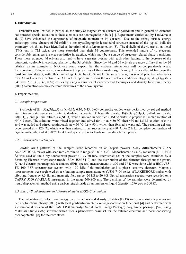
Powder XRD pattern of the samples S1-S4 are sown are shown in Fig. 1. The XRD data were analyzed by the FullProf Suite (version 3.90) software package [9] to determine the unit cell parameters and indexing. All the oxides crystallized in tetragonal phase with lattice parameters: A = 8.6157, 8.6267, 8.6228 and 8.6256 Å; C = 5.9183, 5.9274, 5.9104 and 5.9148 Å in S1-S4, respectively and space group I4/mcm. By comparing the observed densities of the samples with the corresponding calculated ones the value of the number of formula units in unit cell, Z, is determined to be 1. The ratios of the lattice parameters C/A are 0.6869, 0.6871, 0.6854 and 0.6857 for S1-S4, respectively. From the C/A ratios, it is observed that there is no change in the tetragonality of the samples. From the result we infer that progressive substitution of Bi and Pd by Ga, the tetragonal structure is maintained upto x=0.60. The lattice parameters and the related data are shown in Table 1. The average crystallite sizes determined by Scherrer relation [10] are found to be ~ 27-32 nm indicating the formation of nanoparticles in the oxides.
Fig. 1 Powder XRD patterns with indexed lattice planes of Bi2+xGaxPd4-3xO (S1-S4: x=0.15, 0.30, 0.45 & 0.60)
Table 1. cal obs and average crystallite sizes in Bi2+xGaxPd4-3xO
Unit cell parameters/Sample
(S1-S4: x=0.15, 0.30, 0.45, 0.60) oxides
S1 S2 S3 S4
Unit cell Tetragonal Tetragonal Tetragonal Tetragonal
Aa (Å)
Ca
8.6354
5.8786(Å)
8.6420
5.9099
8.6241
5.9122
8.6272
5.9161
Unit cell volumea (Å3 439.32) 441.12 439.45 440.06
Space group I4/mcm I4/mcm I4/mcm I4/mcm
Z 1 1 1 1
cal 3.557(g/cc) 3.472 3.422 3.354
obs 3.365(g/cc) 3.423 3.425 2.892
Average crystallite size (nm) 27 30 32 31
a After refinement
3.2. SEM Studies
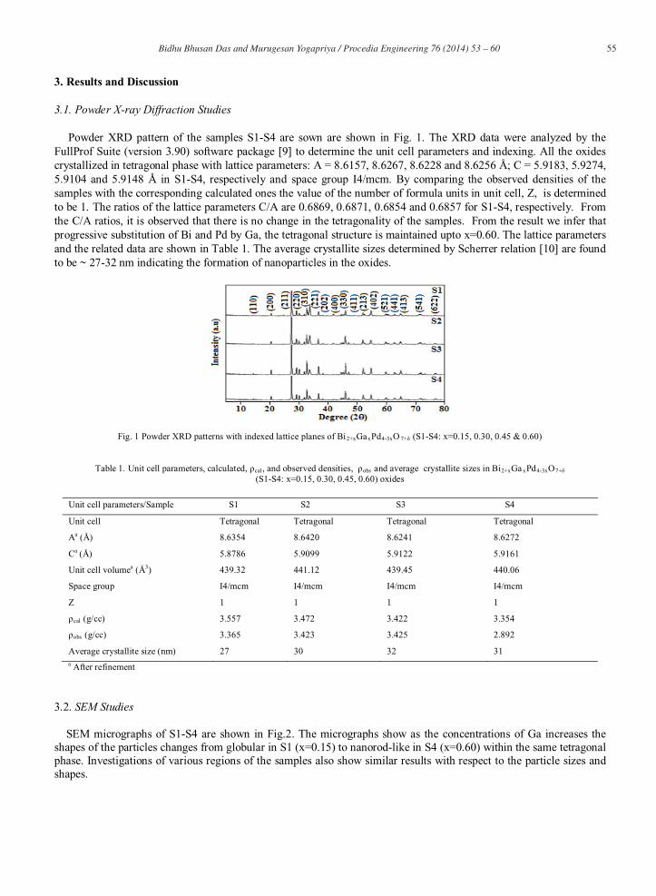
SEM micrographs of S1-S4 are shown in Fig.2. The micrographs show as the concentrations of Ga increases the shapes of the particles changes from globular in S1 (x=0.15) to nanorod-like in S4 (x=0.60) within the same tetragonal phase. Investigations of various regions of the samples also show similar results with respect to the particle sizes and shapes.
56 Bidhu Bhusan Das and Murugesan Yogapriya / Procedia Engineering 76 ( 2014 ) 53 – 60
Fig.2 SEM micrographs of Bi2+xGaxPd4-3xO (S1-S4: x=0.15, 0.30, 0.45, 0.60) at different magnifications.
3.3 Crystal Structure Refinement and Fourier Electron Density Mapping
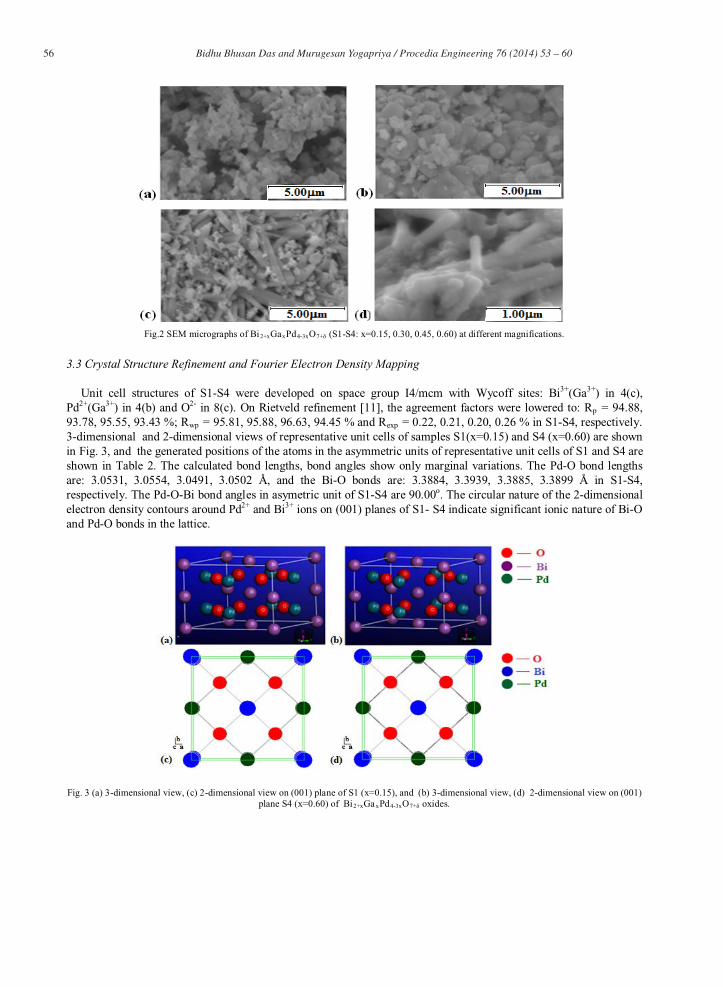
Unit cell structures of S1-S4 were developed on space group I4/mcm with Wycoff sites: Bi3+(Ga3+) in 4(c), Pd2+(Ga3+) in 4(b) and O2- in 8(c). On Rietveld refinement [11], the agreement factors were lowered to: Rp = 94.88, 93.78, 95.55, 93.43 %; Rwp = 95.81, 95.88, 96.63, 94.45 % and Rexp = 0.22, 0.21, 0.20, 0.26 % in S1-S4, respectively. 3-dimensional and 2-dimensional views of representative unit cells of samples S1(x=0.15) and S4 (x=0.60) are shown in Fig. 3, and the generated positions of the atoms in the asymmetric units of representative unit cells of S1 and S4 are shown in Table 2. The calculated bond lengths, bond angles show only marginal variations. The Pd-O bond lengths are: 3.0531, 3.0554, 3.0491, 3.0502 Å, and the Bi-O bonds are: 3.3884, 3.3939, 3.3885, 3.3899 Å in S1-S4, respectively. The Pd-O-Bi bond angles in asymetric unit of S1-S4 are 90.00o. The circular nature of the 2-dimensional electron density contours around Pd2+ and Bi3+ ions on (001) planes of S1- S4 indicate significant ionic nature of Bi-Oand Pd-O bonds in the lattice.
Fig. 3 (a) 3-dimensional view, (c) 2-dimensional view on (001) plane of S1 (x=0.15), and (b) 3-dimensional view, (d) 2-dimensional view on (001) plane S4 (x=0.60) of Bi2+xGaxPd4-3xO oxides.

57 Bidhu Bhusan Das and Murugesan Yogapriya / Procedia Engineering 76 ( 2014 ) 53 – 60
Table 2 Generated positions of atoms in the asymmetric unit of S1 (x=0.15) and S4 (x=0.60) of Bi2+xGaxPd4-3xO
Sl.
No Name
oxides.
Crystal coordinates Cartesean coordinates before refinement Cartesean coordinates after refinement
x y z X Y Z X Y Z
S1
1 Pd 0.0000 0.5000 0.2500 -4.3079 0.0000 -1.4796 -4.3177 0.0000 -1.4697
2 Bi 0.0000 0.0000 0.0000 -4.3080 -4.3079 -2.9591 -4.3178 -4.3177 -2.9393
3 O 0.2500 0.2500 0.2500 -2.1540 -2.1540 -1.4796 -2.1589 -2.1589 -1.4697
S4
1 Pd 0.0000 0.5000 0.2500 -4.3124 0.0000 -1.4787 -4.3136 0.0000 -1.4790
2 Bi 0.0000 0.0000 0.0000 -4.3125 -4.3124 -2.9575 -4.3137 -4.3136 -2.9581
3 O 0.2500 0.2500 0.2500 -2.1562 -2.1562 -1.4787 -2.1568 -2.1568 -1.4790
3.4. Electronic Energy Band Structure and Density of States (DOS) Studies
Figs. 4(a)-(b) and Figs. 4(c)-(d) show the energy band structures and DOS of S1 and S4, respectively. The Fermi level, EF, is pinned at 0 eV. A smearing of 0.5 eV was used to generate the DOS plots. Band gap, Eg, is ~ 0.02 eV in S1-S4. Band in the range -4.0 to 1.0 eV is the valence band (VB) and is mainly due to O2p, Pd 4d, Bi 6p and Ga-4p orbitals. The p states extend over the higher part of the VB, where they mix with the Pd 4d states which are broadened over ~ 6 eV. This is due to Pd belonging to the second TM series and to the mixing with the Bi and Ga p states as detailed in the narrow energy PDOS shown in Fig. 4(e). The large dispersed band is centered well below the EF.Then, EF is crossed by low intensity itinerant s, p states arising from all constituent atoms. In a band structure description, these will be signaled by a large dispersion band, i.e. contrary to flat localized bands characterizing d (and f) subshells. The band gap opening in S1-S4 is a consequence of the octahedral crystal field with tetragonal distortion splitting of the Pd 4d orbitals [12]. The generalized gradient approximation (GGA) calculations performed in the present work were also unable to reproduce the gap. Band gap underestimation in semiconductors is a well known limitation. As compared with the calculated Eg ~ 0.02 eV the experimental band gap energies are : Eg = 1.38, 1.43, 1.40, 1.52 in S1-S4, respectively as discussed in Section 3.7. A large DOS is present at EF for the Pd atom if the spin parity constraint is imposed, which might induce weak localized ferromagnetic behavior [13]. The band ~ -3 to 1 eV is attributed to Pd 4d and 4s states. The bands between ~ -7 to 12 eV are due to Bi 5s, 5p and Ga 3s orbitals. The bands lying between -17 and -15 eV are almost contributions from O 2p states. The DOS is higher for O 2p states (the largest DOS of 25 electrons/eV) than Bi 6p states (the largest DOS of 8 electrons/eV). It means that some of the electrons from Bi 6p transform into the valence bands comprising mainly O 2p orbitals and take part in partialcovalence interactions between Bi and O atoms.
Fig. 4 Partial density of states of Bi, O, Ga, Pd in S4

58 Bidhu Bhusan Das and Murugesan Yogapriya / Procedia Engineering 76 ( 2014 ) 53 – 60
3.5. Electron Paramagnetic Resonance (EPR) Spectroscopic Studies
Fig. 5(a)-(b) shows the EPR lineshapes of S1-S4 recorded at 300 K and 77 K, respectively. EPR lineshapes show two giso- values each: g1= 4.260, 4.201, 4.184, 4.186; g2= 2.024, 2.018, 2.010, 2.033 at 300 K and g3 = 4.423, 4.186, 4.209, 4.204; g4 = 2.148, 2.148, 2.041, 2.051 at 77 K. At 77 K, the g4 signal is better observable which shows hyperfine splitting due to l05Pd (I=5/2; relative abundance 22.6%)[14] at both Pd+(4d9) and Pd2+(4d8) sites in S1-S4.This signal with poor hyperfine feature or as isotropic signal at g2 at 300 K is also observed. The giso-values ~ 4.184 -4.423 are normally due to the presence of Fe3+ ions as magnetic impurity as encountered in TM ion matrices or could be the artefact from the EPR cavity.
Fig. 5 Observed EPR lineshapes at (a) 300 K, (b) 77 K of S1-S4 and (c) expanded lineshapes at 77 K of S1 and S2.
Table 3. Observed giso -values in S1-S4 of Bi2+xGaxPd4-3xO
Sl. No.
(0.15
giso g– values at 300 K____________________g1 g2
iso – values at 77 K______________________g3 g4
S1 4.260 2.024 4.423 2.148
S2 4.201 2.018 4.186 2.148
S3
S4
4.184 2.010
4.186 2.033
4.209 2.041
4.204 2.051
3.6. Magnetic Studies
The magnetic moment versus magnetic field plots of S1-S4 show hysteresis loop in the range -20 kG to +20 kG (Fig. 6) at 300 K. The values of the coercivity, retentivity, magnetic susceptibility of the samples are shown in Table 4. The fairly low values of the coercivity, retentivity and magnetic susceptibility ~ 1.190-8.533 emu/gG show fairly weak ferromagnetic [15] nature of the samples. The powder XRD patterns refinement of S1-S4 shows that the variations in a, c and a/c ratios are < 0.3 % with no cahnge in local symmetry; the average crystallite sizes are also inthe range 27-32 nm. This shows that the relative concentrations of the magnetic Pd2+ and or Pd1+ ions distributed in 4(b) Wycoff sites could be the source of weak ferromagnetism in S1-S4. The Table 4 also shows that the variations in magnetic in S1(x=0.15)- S4(x=0.60) do not show any regularity with the increasing values of x with progressive substitution of diamagnetic Bi3+ and magnetic Pd2+ by diamagnetic Ga3+ ions in the crystal lattice.
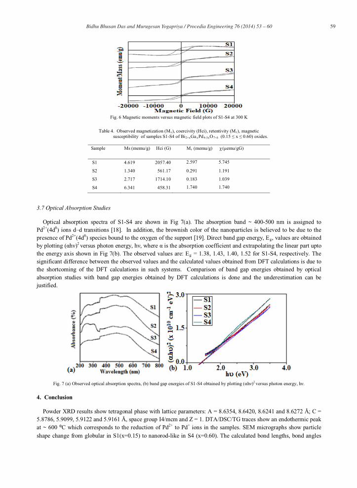
59 Bidhu Bhusan Das and Murugesan Yogapriya / Procedia Engineering 76 ( 2014 ) 53 – 60
Fig. 6 Magnetic moments versus magnetic field plots of S1-S4 at 300 K
Table 4. Observed magnetization (Ms), coercivity (Hci), retentivity (Mr), magnetic susceptibility of samples S1-S4 of Bi2+xGaxPd4-3xO
Sample
(0.15
Ms (memu/g) Hci (G) Mr (memu/g ( emu/gG)
S1 4.619 2057.40 2.597 5.745
S2 1.340 561.17 0.291 1.191
S3
S4
2.717 1714.10
6.341 458.31
0.183 1.039
1.740 1.740
3.7 Optical Absorption Studies
Optical absorption spectra of S1-S4 are shown in Fig 7(a). The absorption band ~ 400-500 nm is assigned to Pd2+(4d8) ions d–d transitions [18]. In addition, the brownish color of the nanoparticles is believed to be due to the presence of Pd2+(4d8) species bound to the oxygen of the support [19]. Direct band gap energy, Eg, values are obtained
2 where is the absorption coefficient and extrapolating the linear part upto the energy axis shown in Fig 7(b). The observed values are: Eg = 1.38, 1.43, 1.40, 1.52 for S1-S4, respectively. The significant difference between the observed values and the calculated values obtained from DFT calculations is due to the shortcoming of the DFT calculations in such systems. Comparison of band gap energies obtained by optical absorption studies with band gap energies obtained by DFT calculations is done and the underestimation can be justified.
Fig. 7 (a) Observed optical absorption spectra, (b) band gap energies of S1-S4 2
Powder XRD results show tetragonal phase with lattice parameters: A = 8.6354, 8.6420, 8.6241 and 8.6272 Å; C = 5.8786, 5.9099, 5.9122 and 5.9161 Å, space group I4/mcm and Z = 1. DTA/DSC/TG traces show an endothermic peak at ~ 600 C which corresponds to the reduction of Pd
versus photon energy, h .
4. Conclusion
2+ to Pd+ ions in the samples. SEM micrographs show particle shape change from globular in S1(x=0.15) to nanorod-like in S4 (x=0.60). The calculated bond lengths, bond angles

60 Bidhu Bhusan Das and Murugesan Yogapriya / Procedia Engineering 76 ( 2014 ) 53 – 60
show only marginal variations in the samples. The energy band gap, Eg, in the samples are found to be ~ 0.02 eV in S1-S4. Observed EPR lineshapes show two giso-values each at 300 K and at 77 K in S1-S4. The giso-values ~2.010-2.033 at 300 K, and giso-values ~ 2.041-2.148 at 77 K are due to Pd+(4d9) and Pd2+(4d8) (105Pd, I=5/2, abundance ~ 22.2%). While the giso-values ~ 4.0 at 300 K and at 77 K is attributed to the presence of magnetic impurity ions in the samples. Presence of hysteresis loops with very low values of the coercivity, retentivity and magnetic susceptibility ~1.190-8.533 emu/gG show fairly weak ferromagnetic nature of the samples at 300 K. Optical absorption band between 400-500 nm is due to the d–d transitions in Pd2+(4d8) ions. Observed Eg
[11] McCusker, L.B., Dreele, R.B.V., Cox, D.E., Louër, D., Scardi, P., 1999. Rietveld refinement guidelines, Journal of Applied Crystallography
values: 1.38, 1.43, 1.40, 1.52 of S1-S4, respectively show semiconducting nature of the materials.
Acknowledgements
The authors thank Dr. M M Balakrishnarajan for help with the Materials Studio (MS) software.
References
[1] Kumar, V., Kawazoe, Y., 2003. Magnetism in clusters of non-magnetic elements: Pd, Rh, and Ru, European Physics Journal D 24, p.81.[2] Taniyama, T., Ohta, E., Sato, T., 1997. Observation of 4d ferromagnetism in free-standing Pd fine particles, Europhysics Letters 38(3), p.195. [3] Litrán, R., Sampedro, I.B., Rojas, T.C., Multigner, M., Sánchez-López, J.C., Crespo, P., López-Cartes, C., García, M.A., Hernando, A.,
Fernández, A., 2006. Magnetic and microstructural analysis of palladium nanoparticles with different capping systems, Physical Review B 73, p.054404.
[4] Perdew, J.P., Burke, K., Ernzerhof, M., 1996. Generalized Gradient Approximation Made Simple, Physics Review Letters 77, p.3865.[5] Payne, M.C., Teter, M.P., Allan, D.C., Arias, T.A., Joannopoulos, J.D., 1992. Iterative minimization techniques for ab initio total energy calculations: molecular dynamics and conjugate gradients, Review of Modern Physics 64, p.1045. [6] Segall, M.D., Lindan, P.L.D., Probert, M.I.J., Pickard, C.J., Hasnip, P.J., Clark, S.J., Payne, M.C., 2002. First-principles simulation: ideas, illustrations and the CASTEP code, Journal of Physics: Condense Matter 14, p.2717. [7] Clark, S.J., Segall, M.D., Pickard, C.J., Hasnip, P.J., Probert, M.I.J., Refson, K., Payne, M.C., 2005. First principles methods using CASTEP, Zeitscript fur Kristallographie 220(5- 6), p.567.[8] Hamman, D.R., Schlüter, M., Chiang, C., 1979. Norm-Conserving Pseudopotentials, Physics Review Letters 43, p.1494. [9] Carjaval, J.R., FULLPROF program, Rietveld Pattern Matching Analysis of Powder Patterns, ILL, Grenoble, 1990.
[10] Klug, H.P., Alexander, L.E., 1997. X-ray Diffraction procedures for polycrystalline and amorphous Materials, 2nd ed., John Wiley & Sons. Ltd, New York, p.966.
32, p.36.[12] Park, K.T., Novikov, D.L., Gubanov, V.A., Freeman, A., 1994. Electronic structure of noble-metal monoxides: PdO, PtO, and AgO, Physical Review B 49, p.4425.[13] ez Calbet, J., Vallet, M., 2003. Ferromagnetism in fcc Twinned 2.4 nm Size Pd Nanoparticles, Physical Review Letters 91, p.237203. [14] Abragam, A., Bleaney, B., 1970. Electron Paramagnetc Resonance of Transition Ions, Oxford University Press, Oxford, U.K.15] Oba, Y., Shinohara, T., Oku, T., Suzuki, J., Ohnuma, M., Sato, T., 2009. Magnetic Intraparticle Structure in Ferromagnetic Pd Nanoparticle, Journal of Physical Society of Japan 78, p.044711/1.[16] Delin, A., Tosatti, E., Weht, R., 2004. Magnetism in Atomic-Size Palladium Contacts and Nanowires, Physical Review Letters 92, p.057201.[17] Blugel, S., 1992. Two-Dimensional Ferromagnetism of 3d, 4d, and 5d Transition Metal Monolayers on Nobel Metal (001) Substartes, Physical Review Letters 68, p.851.[18] Pestryakov, A.N., Lunin, V.V., Fuentes, S., Bogdanchikova, N., Barrera, A., 2003. Influence of modifying additives on the electronic state of supported palladium, Chemical Physics Letters 367, p.102.[19] Panin, V., Khasanova, N.R., Bougerol, C., Schnelle, W., Tendeloo, G.V., Antipov, E.V., 2010. Ordering of Pd2+ and Pd4+ in the Mixed-Valent Palladate KPd2O3, Inorganic Chemistry 49, p.1295.