Synthesis and Characterization of Self-Assembly-Based ...
197
Synthesis and Characterization of Self-Assembly-Based Mesoporous Organosilica Films for Low-k Dielectric Application Murad Aydan Redzheb Student number: 01210640 Supervisors: Prof. Dr. Pascal Van Der Voort, Dr. Silvia Armini A dissertation submitted to Ghent University in partial fulfilment of the requirements for the degree of Doctor in Sciences - Chemistry Academic year: 2017 – 2018
Transcript of Synthesis and Characterization of Self-Assembly-Based ...

Synthesis and Characterization of
Self-Assembly-Based
Mesoporous Organosilica Films
for Low-k Dielectric Application
Murad Aydan Redzheb Student number: 01210640
Supervisors: Prof. Dr. Pascal Van Der Voort, Dr. Silvia Armini
A dissertation submitted to Ghent University in partial fulfilment of the requirements for the degree of
Doctor in Sciences - Chemistry
Academic year: 2017 – 2018


i
Table of Contents
Table of Contents ............................................................................................................................................. i
ACKNOWLEDGEMENTS ............................................................................................................................. v
SCIENTIFIC ACTIVITIES.............................................................................................................................. vii
ENGLISH SUMMARY ..................................................................................................................................... ix
NEDERLANDSE SAMENVATTING .......................................................................................................... xii
ABBREVIATIONS .......................................................................................................................................... xv
CHAPTER 1. INTRODUCTION ................................................................................................................. 1
1.1. Ultra-large scale integrated circuits, Back-End-Of-Line and low-k materials ........................ 1
1.2. Dielectric constant .............................................................................................................................. 4
1.3. Historical overview of low-k materials .......................................................................................... 6
1.4. Low-k deposition methods ............................................................................................................ 11
1.4.1. Plasma-enhanced chemical vapor deposition (PECVD) .................................................. 11
1.4.2. Spin-on deposition ................................................................................................................... 12
1.5. Low-k candidates .............................................................................................................................. 15
1.5.1. Silicates and zeolites ................................................................................................................ 16
1.5.2. Polymers ..................................................................................................................................... 22
1.5.3. Organosilicates ......................................................................................................................... 24
1.5.4. Non-silicon-based low-k dielectrics .................................................................................... 33
1.6. Periodic mesoporous silica-based materials .............................................................................. 34
1.6.1. Mechanism of formation: self-assembly .............................................................................. 35
1.6.2. Periodic mesoporous silica films for low-k ........................................................................ 39
1.6.3. Periodic mesoporous organosilica films for low-k ........................................................... 41
1.7. Goal of the PhD research .............................................................................................................. 42
1.8. References .......................................................................................................................................... 43
CHAPTER 2. EFFECT OF UV CURE ON OXYCARBOSILANE LOW-K PROPERTIES ........... 55
2.1. Introduction ....................................................................................................................................... 56
2.2. Experimental Section ....................................................................................................................... 57

ii
2.3. Results and Discussion .................................................................................................................... 58
2.3.1. Effect of the C-bridge length on the UV resistance of oxycarbosilanes films ........... 58
2.3.2. UV cure of methylene-bridged oxycarbosilanes low-k films with a target k=2.2 ..... 63
2.3.3. UV cure of methylene-bridged oxycarbosilanes low-k films with a target k=2.0 ..... 71
2.4. Conclusions ....................................................................................................................................... 73
2.5. References .......................................................................................................................................... 73
CHAPTER 3. EFFECT OF LASER ANNEAL ON OXYCARBOSILANE LOW-K PROPERTIES77
3.1. Introduction ....................................................................................................................................... 78
3.2. Experimental Section ....................................................................................................................... 78
3.3. Results and Discussion .................................................................................................................... 79
3.3.1. Screening for laser anneal conditions for oxycarbosilanes low-k films ....................... 79
3.3.2. IR laser anneal in a controlled inert atmosphere ............................................................. 81
3.4. Conclusions ....................................................................................................................................... 84
3.5. References .......................................................................................................................................... 84
CHAPTER 4. PROPERTIES OF SELF-ASSEMBLY-BASED LOW-K FILMS: EFFECT OF THE
REPLACEMENT OF SI-O-SI BY SI-CH2-SI.............................................................................................. 87
4.1. Introduction ....................................................................................................................................... 88
4.2. Experimental Section ....................................................................................................................... 89
4.3. Results and Discussion .................................................................................................................... 91
4.3.1. Chemical composition of OCS and MSQ films ................................................................. 91
4.3.2. Pore structure of OCS and MSQ films ............................................................................... 94
4.3.3. Mechanical and dielectric properties of OCS and MSQ films ....................................... 96
4.3.4. HF stability of the MSQ and OCS films .............................................................................. 99
4.3.5. Template dependence of electrical reliability .................................................................. 103
4.4. Conclusions ..................................................................................................................................... 105
4.5. References ........................................................................................................................................ 105
CHAPTER 5. TEMPLATE-DEPENDENT HYDROPHOBICITY IN MESOPOROUS
ORGANOSILICA FILMS ........................................................................................................................... 111
5.1. Introduction ..................................................................................................................................... 112

iii
5.2. Experimental Section ..................................................................................................................... 113
5.3. Results and Discussion .................................................................................................................. 113
5.4. Conclusions ..................................................................................................................................... 120
5.5. References ........................................................................................................................................ 121
CHAPTER 6. GEMINI-TEMPLATED PMO FILMS ............................................................................... 123
6.1. Introduction ..................................................................................................................................... 124
6.2. Experimental Section ..................................................................................................................... 124
6.3. Results and Discussion .................................................................................................................. 125
6.4. Conclusions ..................................................................................................................................... 129
6.5. References ........................................................................................................................................ 129
CHAPTER 7. TIME-RESOLVED GISAXS INVESTIGATION OF THE SELF-ASSEMBLY OF SPIN-
COATED PMO FILMS ............................................................................................................................... 131
7.1. Introduction ..................................................................................................................................... 132
7.2. Experimental Section ..................................................................................................................... 133
7.3. Results and Discussion .................................................................................................................. 134
7.4. Conclusions ..................................................................................................................................... 143
7.5. References ........................................................................................................................................ 144
CHAPTER 8. PERIODIC MESOPOROUS ORGANOSILICA FILMS FOR LOW-K
APPLICATION: PROMISES AND CHALLENGES .............................................................................. 147
8.1. Introduction ..................................................................................................................................... 148
8.2. Experimental Section ..................................................................................................................... 149
8.3. Results and Discussion .................................................................................................................. 150
8.3.1. Effect of pore order on Young’s modulus ........................................................................ 150
8.3.2. PMO film deposition in 45 nm trenches ........................................................................... 153
8.3.3. Effect of the template on the electrical reliability of PMO films ................................. 155
8.4. Conclusions ..................................................................................................................................... 157
8.5. References ........................................................................................................................................ 157
CHAPTER 9. GENERAL CONCLUSIONS AND OUTLOOK ....................................................... 159
9.1. General conclusions ....................................................................................................................... 159

iv
9.1.1. Conclusions on electromagnetic activation of the C-bridged low-k ......................... 159
9.1.2. Conclusions on the replacement of siloxane bonds by alkylene groups .................. 159
9.1.3. Conclusions on PMO hydrophobicity ............................................................................... 160
9.1.4. Conclusions on Gemini-templated PMO ......................................................................... 160
9.1.5. Conclusions on PMO for low-k .......................................................................................... 160
9.1.6. Conclusions on the suitability of ionic surfactants as a low-k template ................... 161
9.2. Outlook ............................................................................................................................................ 161
9.2.1. Concerning PMO for low-k application ............................................................................ 161
9.2.2. Area-selective deposition of low-k .................................................................................... 163
9.2.2.1. Introduction ......................................................................................................................... 163
9.2.2.3. Results and Discussion ...................................................................................................... 164
9.2.2.4. Selectivity mechanism ........................................................................................................ 166
9.2.2.5. Conclusions and outlook .................................................................................................. 167
9.3. References ........................................................................................................................................ 168
APPENDIX A. METHODOLOGY .......................................................................................................... 169
A1. Spectroscopic Ellipsometry (SE).................................................................................................. 169
A2. Ellipsometric Porosimetry (EP) ................................................................................................... 169
A3. Fourier-Transform Infra-Red Spectroscopy (FTIR) ................................................................ 171
A4. Nanoindentation (NI) .................................................................................................................... 172
A5. Impedance Spectroscopy .............................................................................................................. 173
A6. Grazing-Incidence Small-Angle X-Ray Scattering (GISAXS) ................................................. 173
A7. X-Ray Photoelectron Spectroscopy (XPS) ............................................................................... 176
A8. Time-of-Flight Secondary Ion Mass Spectroscopy (TOF-SIMS) ........................................... 176
A9. Chemical stability ............................................................................................................................ 177
A10. References ...................................................................................................................................... 177

v
ACKNOWLEDGEMENTS
Before starting my doctoral studies, I had the chance to spend nine months in imec. During this
period, I got an impression of a collaborative atmosphere created and maintained by people who
were always ready to respond to a request for help and eager to explain in detail the source of
and the solutions to my problems. These impressions convinced me that imec would be a
wonderful place to conduct a PhD research.
My PhD experience, however, was made possible by my promotor Prof. Dr. Pascal Van Der
Voort, my former co-promotor Dr. Mikhail R. Baklanov and my current co-promotor Dr. Silvia
Armini. Therefore, I would like to thank them for giving me the opportunity to start this PhD
research and for their guidance during my studies.
In addition to the discussions with promotors, my PhD activities were significantly influenced by
discussions with and contributions from PhD colleagues whose work involved development of
low-k materials. In particular, I thank Mikhail Krishtab, Liping Zhang, Oguzhan Orkut Okudur,
and Chen Wu. I am also grateful for the feedback which I received during the regular low-k
meetings from the usual attendees Quoc Toan Le, Patrick Verdonck, Jean-Francois de Marneffe,
and Kris Vanstreels. Furthermore, I thank the colleagues and friends Marcus Heyne, Yiting Sun,
Ivan Zyulkov, Sebastiaan Herregods, Benjamin Groven, Davide Tierno, Abhitosh Vais, Sebastien
Moitzheim, and Tsvetan Ivanov with whom we shared many lunches and interesting
conversations.
As a part of the PhD experience, I had the chance to enjoy the mentoring of internship and
thesis students. This experience made me appreciate the various motivations and the associated
attitudes toward scientific contributions students can have. I thank Henry Hopkins, Tom Berger,
Mathias Jacobs, Laura Garcia Gonzalez, and Jens Van Nerum for their contributions.
Imec has an exceptionally rich portfolio of characterization techniques which enable fast material
characterization which is crucial for a material development research. These techniques are
mainly operated by the colleagues at the material and components analysis department of which
I would like to thank Johan Meersschaut, Olivier Richard, Thierry Conard, and Alexis Franquet.
Another rare opportunity accessible to PhD students at imec is the access to clean rooms
equipped with not only the tools which are employed for the production of the current
generation of integrated circuits but also with the tools which will be required for the future
generation technology nodes. However, getting familiar with the tool capabilities and process
peculiarities would be challenging were it not for the integration engineers and the managers. In
this respect, I thank Gayle Murdoch, Hirohisa Uchida, Juergen Boemmels, Zsolt Tokei, and
Herbert Struyf for their support.

vi
In spite of being a Ghent University student, due to my accommodation in Leuven, I did not have
too many opportunities to interact with my UGent colleagues. However, I would like to thank
Frederik Goethals, Els De Canck, and Sander Clerick for their assistance and their readiness to
help a distant colleague.
Apart from the two main institutions which enabled my PhD studies, I was fortunate enough to
collaborate with the Leibniz Institute of Surface Modification in Leipzig, Germany. This
collaboration was made possible by Lutz Prager who readily agreed to host me for a week of
UV cure experiments in his lab. I thank Dr. Prager for his hospitality and for the delightful tour
of the Leipzig centre. I also thank Sergej Naumov for his quantum chemical calculations which
helped us better understand the UV cure results.
SBA Materials, Inc. are acknowledged for providing films for investigation of the effect of the UV
cure on the low-k properties as well as for their financial support in meeting the cost associated
with the trip to Leipzig. In particular, I thank Hash Pakbaz, James Hickman, and Nigel Hacker.
Ultratech, Inc. are acknowledged for performing laser anneal experiments on the low-k films. In
particular, I thank Michael Awdshiew, Yun Wang, Shaoyin Chen, and Van Le.
The grazing-incidence small-angle x-ray scattering (GISAXS) experiments in the ELETTRA
synchrotron facility in Trieste, Italy are another memorable experience from my PhD years. In
this regard, I would especially like to thank Sigrid Bernstorff who agreed to collaborate with
people (me and Silvia) who had no experience with GISAXS measurements or GISAXS data
analysis. I thank Dr. Bernstorff for accommodating us on two occasions in her personal beam
time which allowed us to prepare a successful proposal for a comprehensive GISAXS study. I
also thank Krunoslav Juraic and Barbara Sartori without whom the GISAXS experiments
wouldn’t have been possible.
Finally, I thank my mother, Sevil Keskin, and my best friend and partner in life Fevi for their loving
support.

vii
SCIENTIFIC ACTIVITIES
Peer Reviewed Journals
1. M. Redzheb, L. Prager, S. Naumov, M. Krishtab, S. Armini, P. Van Der Voort, M. R. Baklanov, Effect of the
C-bridge length on the ultraviolet-resistance of oxycarbosilane low-k films, Applied Physics Letters, 108(1),
012902 (2016)
2. M. Redzheb, L. Prager, M. Krishtab, S. Armini, K. Vanstreels, A. Franquet, P. Van Der Voort, M.R. Baklanov,
UV cure of oxycarbosilane low-k films, Microelectronic Engineering, 156, 103-107 (2016)
3. M. Redzheb, S. Armini, T. Berger, M. Jacobs, M. Krishtab, K. Vanstreels, S. Bernstorff and P. Van Der Voort,
On the mechanical and electrical properties of self-assembly-based organosilicate porous films, Journal of
Materials Chemistry C, 5, 8599-8607 (2017)
4. M. Redzheb, S. Bernstorff, B. Sartori, P. Van Der Voort, S. Armini, Periodic Mesoporous Organosilica Films
with a Tunable Steady-State Mesophase, ChemPhysChem, 18, 20, 2846–2849 (2017)
5. M. Redzheb, P. Van Der Voort, S. Armini, Template dependent hydrophobicity in mesoporous organosilica
films, Microporous and Mesoporous Materials, In press, Available online 7 October 2017
Conference Proceedings
1. M. Redzheb, L. Prager, M. Krishtab, S. Armini, K. Vanstreels, A. Franquet, P. Van Der Voort, M.R. Baklanov,
Impact of UV wavelength and curing time on the properties of spin-coated low-k films, 2015 IEEE International
Interconnect Technology Conference and 2015 IEEE Materials for Advanced Metallization Conference
(IITC/MAM), 99-102 (2015)
2. M. Redzheb, S. Armini, K. Vanstreels, J. Meersschaut, M. R. Baklanov, Y. Wang, S. Chen, V. Le, M. Awdshiew,
P. Van Der Voort, Laser anneal of oxycarbosilane low-k film, 2016 IEEE International Interconnect Technology
Conference / Advanced Metallization Conference (IITC/AMC), 156-158 (2016)
Patents
1. M. Redzheb, S. Armini, Selective deposition of dielectric materials, EP 17169473, Priority date 04.05.2017
Conferences
1. M. Redzheb, S. Armini, M. Baklanov, P Van Der Voort, Characterization of advanced k 1.9, 2.0 and 2.2 ultra-
porous SiOC(H) films deposited by Plasma-Enhanced Chemical Vapor Deposition, Science and Application of
Thin Films, 2014, Çeș me, Turkey (oral)
2. M. Redzheb, L. Prager, M.Krishtab, S. Armini, K. Vanstreels, Alexis Franquet, P. Van Der Voort, and M.R.
Baklanov, Impact of UV wavelength and curing time on the properties of spincoated low-k films, International
Interconnect Technology Conference / Materials for Advanced Metallization 2015, Grenoble, France (poster)
3. M. Redzheb, S. Armini, O. O. Okudur, K. Vanstreels, S. Bernstorff, P. Van Der Voort and M. Baklanov, Gemini-
templated PMO low-k films, Materials for Advanced Metallization, 2016, Brussels, Belgium (oral)
4. M. Redzheb, S. Armini, K. Vanstreels, J. Meersschaut, M.R. Baklanov, Y. Wang, S. Chen, V. Le, M. Awdshiew,
P. Van Der Voort, Laser anneal of oxycarbosilane low-k film, International Interconnect Technology Conference
/ Advanced Metallization Conference 2016, San Jose, California, USA (poster)

viii
5. M. Redzheb, S. Armini, B. Sartori, S. Bernstorff, P. Van Der Voort, Time-resolved GISAXS investigation of the
self-assembly of spin-coated PMO films, XXV International Materials Research Congress, 2016, Cancun,
Mexico (oral)
6. M. Redzheb, O. O. Okudur, P. Van Der Voort, S. Armini, Periodic Mesoporous Organosilica Films for Low-k
Application: Promises and Challenges, MRS Spring Meeting and Exhibit, 2017, Phoenix, AZ, USA (oral)
7. M. Redzheb, P. Van Der Voort, S. Armini, Template-dependent hydrophobicity in mesoporous organosilica
films, 5th International Conference on Multifunctiona, Hybrid and Nanomaterials, 2017, Lisbon, Portugal (oral)

ix
ENGLISH SUMMARY
In the last twenty years, the microchip performance has been dominated by the interconnect
(RC) signal delay. Moreover, in contrast to the delay associated with the transistor switching,
the RC delay has steadily increased with each technology node. Thus, various materials have
been investigated to enable faster signal propagation through the interconnects. These efforts
can be divided into two main research areas – conductors and dielectrics. The dielectrics are in
the spotlight of this work. While the insulating properties of the dielectrics, quantified by the
dielectric constant or k-value, are important for the signal delay, the microchip manufacturing
processes impose additional requirements on the insulators, such as mechanical and electrical
reliability, chemical stability, hydrophobicity, thermal stability, and others. Many of these
requirements can be met by self-assembly-based organosilicate dielectrics. In particular,
oxycarbosilane (OCS) and periodic mesoporous organosilica (PMO) films are considered as
promising low-k candidates. Therefore, in this work, we provide additional insight into the
properties of self-assembly based organosilicate films in order to elucidate their applicability as
low-k dielectrics.
Oxycarbosilanes are SiO2-based materials in which some of the Si-O-Si groups have been
replaced by Si-(CH2)x-Si groups. In OCS films, the UV and VUV irradiation has more detrimental
effect on ethylene-bridged (x=2) oxycarbosilane films as compared to those containing
methylene (x=1) groups. The concentration of the bridging ethylene groups is reduced by the
222 nm light. In contrast, the bridging methylene groups are not affected by the 222 nm light.
The difference in the stability of these two alkylene groups is more pronounced when the films
are exposed to 172 nm light. The ethylene groups are depleted by more than 75% while
methylene loss is limited to only 40%. Comparable k and Young’s modulus (YM) values (k≤2.3,
YM≥7.5 GPa and k=2.07, YM=5.5 GPa) are obtained following 1 min 172 nm and 20 min 222 nm
irradiations but the latter produces superior low-k films because of a complete template removal
without any induced hydrophilization. On the other hand, laser anneal can be applied to as-
deposited OCS films for template removal and to improve the YM of the porous films. Within
a narrow processing window, 13% improvement of the YM value as compared to the reference
films annealed in a furnace at 400°C with no impact on the k-value of 2.25 can be achieved.
However, extensive bond rearrangements, mostly related to the removal or reorganization of
the organic content of the organosilicate matrix, make this approach rather unattractive.
The replacement of some of the Si-O-Si by Si-CH2-Si functionalities in a porous organosilica film
results in a smaller improvement of the YM than previously thought. For instance, at a density
of ~0.87 g/cm3, the film containing methylene groups has an YM of 6.6 GPa, while the one without
– 5.3 GPa. This effect is counteracted by a higher dielectric constant for the films containing

x
methylene groups – 2.27 with and 2.12 without the Si-CH2-Si groups at the same density due to
an increase in the matrix density when Si-O-Si are replaced by Si-CH2-Si groups. Therefore,
depending on the integration scheme, if processing damage to the low-k can be avoided, low
carbon content dielectrics might be more suitable for integration due to lower porosity required
to achieve low dielectric constant.
In the organosilica films, the self-hydrophobization reaction in which a bridging methylene group
is transformed into a methyl group can occur at a temperature as low as 200°C, significantly
lower than previously reported in literature. Additionally, the hydrophobization reaction in the
presence of a template requires higher activation energy than in porous materials. Furthermore,
in methylene-bridged organosilica films, the degree of self-hydrophobization depends on the
employed template. The films templated by cetyltrimethylammonium chloride (CTAC) are more
hydrophilic when compared to films templated by BrijL4 and BrijS10. The template-dependent
hydrophobicity is attributed to the blocking of the silanol condensation by the polyethylene
oxide chains in the Brij-type surfactants leading to a higher concentration of Si-OH groups with
respect to CTAC. The extra silanols are consequently available for self-hydrophobization
reactions.
PMO films are OCS films in which control over the pore arrangement allows obtaining pore
structure which belongs to one of the crystallographic groups. We have synthesized and
characterized an ethane-PMO film templated with the ionic Gemini 16-12-16 surfactant.
Following a thermal template removal, the PMO film has a distorted 2D hexagonal pore
organization with a pore size distribution centred at 2 nm. The Gemini-templated PMO films
meet the material specifications for low-k dielectric layers. The Gemini surfactants are an
exciting class of templating molecules because their packing parameter can be relatively easily
controlled, opening the possibility for a systematic engineering of the mesophase of PMO films
with a small pore size.
A tunable steady state (TSS) exists in spin-coated PMO films. During the TSS, the surfactant self-
assembly can be directed by the ambient conditions, such as humidity and temperature, resulting
in a desired mesophase. At a relative humidity of 70%, films with 3D or 2D hexagonal phases
depending on the surfactant to organosilica molar ratio have been obtained. However, the high
humidity has competing effects on the mesophase which can be understood in the context of
the charge density matching mechanism. On the one hand, the interaction between the H2O and
the surfactant molecules leads to an increase of the micelle surface curvature, while on the other
hand, the H2O molecules cause depolymerization of the siloxane bonds creating conditions
which favor the decrease of the micelle surface curvature. The polycondensation degree of the
organosilica oligomers also affects the formed mesophases. For instance, 3D hexagonal phase is
obtained after 20 min solution aging, 2D hexagonal after 40 min aging and no ordered mesophase

xi
if the solution is aged for longer than 70 min. Additionally, cubic mesophases are observed when
the water to organosilica molar ratio is reduced from 30 to 14. A PMO film with a 2D hexagonal
pore order possesses 1.7 GPa lower Young’s modulus than a film with a disordered porosity
while both have the same dielectric constant of 2.30. Experiments to deposit PMO film in narrow
45 nm trenches reveals that high surface energy of the substrate is required in order to obtain
a well-ordered PMO.
Contrary to expectations, the ionic surfactant CTAC is a suitable templating agent for low-k
films. The use of CTAC does not result in a significantly higher leakage current density or lower
breakdown field when compared to a film with a non-ionic surfactant. In particular, the leakage
current density of the CTAC-templated film at 1MV/cm is 1.6x10⁻⁹ A/cm2 while the breakdown
field is 5.7 MV/cm. At the same time, CTAC-templated PMO films have a small pore size of
about 2 nm and a narrow pore size distribution both of which are very important for a low-k
application.

xii
NEDERLANDSE SAMENVATTING
In de afgelopen twintig jaar werd de prestatie van de microchip beperkt door de interconnect
(RC) signaalvertraging. Bovendien is de RC-vertraging, in tegenstelling tot de vertraging die
gepaard gaat met het schakelen van de transistor, gestaag toegenomen met elk
technologieknooppunt. Om hier aan tegemoet te komen zijn er verschillende materialen
onderzocht om een snellere signaalverspreiding door de interconnecties mogelijk te maken.
Deze inspanningen kunnen worden onderverdeeld in twee belangrijke onderzoeksgebieden:
geleiders en dielectrica. Dielectrica zijn de focus van dit werk. Waar de isolerende eigenschappen
van de dielectrica, gemeten door de permittiviteit (diëlektrische constante) of k-waarde,
belangrijk zijn voor de signaalvertraging, stellen de microchip-productieprocessen extra eisen
aan de isolatoren zoals mechanische en elektrische betrouwbaarheid, chemische stabiliteit,
hydrofobiciteit, thermische stabiliteit en andere. Aan veel van deze eisen kan worden voldaan
door self-assembly dieletricia op basis van organosilicaten. Met name oxycarbosilaan (OCS) en
periodieke mesoporeuze organosilica films (PMO-films) worden beschouwd als veelbelovende
kandidaten voor low-k dielectrica. Daarom geven we in dit werk extra inzicht in de
eigenschappen van op self-assembly gebaseerde organosilicaatfilms om hun toepasbaarheid als
low-k dielectrica te verduidelijken.
Oxycarbosilanen zijn materialen op basis van SiO2, waarbij sommige Si-O-Si groepen zijn
vervangen door Si-(CH2)x-Si groepen. In OCS-films hebben UV- en VUV-straling een schadelijker
effect op ethyleen gebrudgde (x=2) oxycarbosilaanfilms dan op methyleen houdende (x=1)
groepen. Fotonen met een energie lager dan 6,2 eV (bv. λ= 222 nm) kunnen de
methyleenbrugverbinding niet vernietigen. De concentratie van de overbruggende
ethyleengroepen wordt daarentegen wel door het 222 nm licht verlaagd. Het verschil in
stabiliteit van deze twee alkyleengroepen is meer uitgesproken wanneer de films worden
blootgesteld aan 172 nm licht. De ethyleengroepen zijn voor meer dan 75% uitgeput, terwijl het
methyleenverlies beperkt is tot slechts 40%. Vergelijkbare k- en Young's modulus (YM)-waarden
(k ≤ 2.3, YM ≥ 7.5 GPa en k = 2.07, YM = 5.5 GPa) worden verkregen na bestraling door 172
nm gedurende 1 minuut of door bestraling 222 nm bestraling gedurende 20 minuten. Deze
laatste produceert superieure low-k films dankzij een complete templaat verwijdering zonder
geïnduceerde hydrofilisatie. Anderzijds kan laser annealing worden toegepast op de vers
afgezette OCS-films voor het verwijderen van templates en ter verbetering van de YM van de
poreuze films. In het strike productieproces kan een verbetering van 13% van de YM-waarde
worden bereikt ten opzichte van de referentiefilm die in een oven bij 400 °C is gebakken en die
verder geen invloed heeft op de k-waarde van 2,25. Door de uitgebreide herschikking van de

xiii
verbindingen, die meestal verband houdt met het verwijderen of reorganiseren van de
organische inhoud van de organosilicaatmatrix, is deze aanpak echter weinig aantrekkelijk.
De vervanging van een deel van de Si-O-Si door Si-CH2-Si functionaliteiten in een poreuze
organosilica film resulteert in een kleinere verbetering van de YM dan eerder gedacht.
Bijvoorbeeld, bij een dichtheid van ~0,87 gcm-3 heeft de film met methyleengroepen een YM van
6,6 GPa, terwijl de film zonder een YM heeft van 5,3 GPa. Dit effect wordt gecompenseerd door
een hogere permittiviteit (diëlektrische constante) voor de films die methyleengroepen bevatten
- 2,27 met en 2,12 zonder Si-CH2-Si-groepen bij dezelfde dichtheid respectievelijk als gevolg van
een toename van de matrixdichtheid wanneer Si-O-Si groepen worden vervangen door Si-CH2-
Si-groepen. Daarom, afhankelijk van het integratie schema, als tijdens het productieproces
schade aan de low-k dielectrica kan worden vermeden, zouden dielectrica met een laag
koolstofgehalte meer geschikt kunnen zijn voor integratie vanwege de lagere porositeit die nodig
is om een lagere permittiviteit te bereiken.
In de organosilica films kan de zelf-hydrofobiseringsreactie waarbij een overbruggende
methyleengroep wordt omgezet in een methylgroep reeds plaats vinden bij een temperatuur
vanaf 200°C, beduidend lager dan eerder vermeld in de literatuur. Bovendien vereist de
hydrofobiseringsreactie in aanwezigheid van een template een hogere activeringsenergie dan in
poreuze materialen. Voorts is de mate van zelf-hydrofobiseringsreactie in methyleen-gebridde
organosilica films afhankelijk van de gebruikte template. De films die door
cetyltrimethylammoniumchloride (CTAC) gebruiken als template, zijn hydrofieler dan films
waarbij BrijL4 en BrijS10 gebruikt werden als template. De template-afhankelijkheid van de
hydrofobiciteit wordt toegeschreven aan het blokkeren van de silanolcondensatie door de
polyethyleenoxidekettingen in oppervlakteactieve stoffen van het Brij type, wat leidt tot een
hogere concentratie van Si-OH-groepen ten opzichte van CTAC. De extra silanolen zijn
bijgevolg dus beschikbaar voor zelf-hydrofobiseringsreacties.
PMO-films zijn OCS-films waarbij de controle over de porieopstelling het mogelijk maakt
poriestructuur te verkrijgen die behoort tot één van de kristallografische groepen. We hebben
een ethaan-PMO film gesynthetiseerd en gekenmerkt waarbij de oppervlakteactieve stof Gemini
16-12-16 als template werd gebruikt. Na het thermisch verwijderen van de template, heeft de
PMO-folie een vervormde 2D zeshoekige poriën sturctuur met een poriëngrootteverdeling
gecentreerd rond 2 nm. De Gemini-gelamineerde PMO-films voldoen aan de
materiaalspecificaties voor low-k diëlektrische lagen. De Gemini oppervlakteactieve stoffen zijn
een interessante klasse van template moleculen omdat hun pakking parameter relatief eenvoudig
te controleren is, waardoor de mogelijkheid ontstaat voor een systematische engineering van
de mesofase van PMO-films met een kleine poriëngrootte.
xiv
In PMO-films met spincoating bestaat een tunable steady state (afstelbare steady state) (TSS).
Tijdens de TSS kan self-assembly door de omgevingscondities, zoals luchtvochtigheid en
temperatuur, gestuurd worden, wat resulteert in een gewenste mesofase. Bij een relatieve
vochtigheid van 70% zijn films met 3D of 2D zeshoekige fasen, afhankelijk van de molaire
verhouding van oppervlakteactieve stof tot organosilica, verkregen. De hoge luchtvochtigheid
heeft echter concurrerende effecten op de mesofase, die kunnen worden begrepen in het kader
van het afstemmingsmechanisme voor de laaddichtheid. Aan de ene kant leidt de interactie
tussen de H2O en de oppervlakteactieve moleculen tot een toename van de kromming van het
micel oppervlak, terwijl aan de andere kant de H2O moleculen leiden tot een depolymerisatie
van de siloxaanbindingen waardoor omstandigheden worden gecreëerd die de afname van de
kromming van het micelle oppervlak bevorderen. De polycondensatiegraad van de organosilica
oligomeren beïnvloedt ook de gevormde mesofasen. Zo wordt bijvoorbeeld een 3D zeshoekige
fase verkregen na 20 min. rijpen van de oplossing, 2D zeshoekig na 40 min. rijpen en geen
geordende mesofase indien de oplossing ouder dan 70 min. is. Bovendien worden kubieke
mesofasen waargenomen wanneer de molaire verhouding van water ten op zichte van organisch-
silica van 30 tot 14 wordt verlaagd. Een PMO-film met een 2D zeshoekige poriënorde heeft een
1,7 GPa lagere Jonge modulus dan een film met een ongeordende porositeit, terwijl beide
dezelfde permittiviteit van 2,30 hebben. Experimenten om PMO-films te deponeren in smalle 45
nm geulen tonen aan dat een hoge oppervlakte-energie van het substraat nodig is om een goed
geordend PMO te verkrijgen.
In tegenstelling tot de verwachtingen is de ionische oppervlakteactieve stof CTAC een geschikt
template voor low-k films. Het gebruik van CTAC leidt niet tot een significant hogere
lekstroomdichtheid of een lager afbraakveld in vergelijking met een film met een niet-ionogene
oppervlakteactieve stof. Met name de lekstroomdichtheid van de CTAC-templated film bij
1MVcm-1 is 1,6 x 10⁻⁹ Acm-2 terwijl het afbraakveld 5,7 MVcm-1 is. Tegelijkertijd hebben PMO-
films waarbij CTAC als template werd gebruikt, een kleine poriegrootte van ongeveer 2 nm en
een smalle poriëndistributie, die beide zeer belangrijk zijn bij low-k toepassingen.

xv
ABBREVIATIONS
AFM Atomic force microscopy
AUC Area under the curve
B3LYP Becke, 3-parameter, Lee-Yang-Parr density functional
BTESE 1,2-Bis(triethoxysilyl)ethane
BTESM 1,2-Bis(triethoxysilyl)methane
CDO Carbon-doped oxide
CMP Chemical-mechanical polishing
CTAB Cetyltrimethylammonium bromide
CTAC Cetyltrimethylammonium chloride
CTE Coefficient of thermal expansion
DEMS Diethoxymethylsilane
DFT Density functional theory
DNA Deoxyribonucleic acid
EISA Evaporation-induced self-assembly
EP Ellipsometric porosimetry
ERD Elastic recoil detection
EtLK Low-k containing ethylene bridges
FER Ferrierite
FinFET Fin Field Effect Transistor
FTIR Fourier-transform infra-red
FWHM Full Width at Half Maximum
GISAXS Grazing-incidence small-angle x-ray scattering
HMDS Hexamethyldisilazane
IBM International business machines
IC Integrated circuit
ITO Indium-Tin-Oxide
LA Laser anneal
LP Low pressure
LTA Linde Type A
MEL ZSM-ELeven
MeLK Low-k containing methylene bridges
MFI ZSM-FIve
MOSFET Metal-Oxide-Semiconductor Field Effect Transistor
MPMOC Methane PMO templated by CTAC

xvi
MPMOL4 Methane PMO templated by BrijL4
MPMOS10 Methane PMO templated by BrijS10
MSE Mean square error
MSQ Methylsilsesquioxane-like film
MSQF127 Methylsilsesquioxane templated by PluronicF127
MSQL4 Methylsilsesquioxane templated by BrijL4
MSQS10 Methylsilsesquioxane templated by BrijS10
MSSQ Methylsilsesquioxane
MTES Methyltriethoxysilane
NASA National Aeronautics and Space Administration
NI Nanoindentation
OCS Oxycarbosilane
OCSF127 Oxycarbosilane templated by PluronicF127
OCSC Oxycarbosilane templated by CTAC
OCSL4 Oxycarbosilane templated by BrijL4
OCSS10 Oxycarbosilane templated by BrijS10
OMCTS Octamethylcyclotetrasiloxane
PECVD Plasma-enhanced chemical vapor deposition
PEO Polyethylene oxide
PID Plasma-induced damage
PMO Periodic mesoporous organosilica
PMS Periodic mesoporous silica
PSD Pore size distribution
PSZ Pure silica-zeolite
RC Resistance x Capacitance
RH Relative humidity
RI Refractive index
RT Room temperature
SAWS Surface acoustic wave spectroscopy
SE Spectroscopic ellipsometry
TDS Thermal desorption spectroscopy
TEM Transmission electron microscopy
TEOS Tetraethoxy silane
TMCS Trimethylchlorosilane
TMS Trimethylsilyl
TMCTS 1,3,5,7-tetramethylcyclotetrasiloxane

xvii
ToF-SIMS Time-of-flight secondary ion mass spectroscopy
TPAOH Tetrapropylammonium hydroxide
ULSI Ultra-large-scale integration
UV Ultra-violet
VUV Vacuum ultra-violet
WCA Water contact angle
XPS X-ray photoemission spectroscopy
XRD X-ray diffraction
YM Young’s modulus
ZSM Zeolite Socony Mobil

xviii

1
CHAPTER 1. INTRODUCTION
1.1. Ultra-large scale integrated circuits, Back-End-Of-Line and low-k materials
What if Moore’s law applied to transportation or to agricultural productivity, or to space travel?
Then, by the year 2017 we would have been able to travel to the Sun on a single gallon of fuel
or feed the world’s population with 1 km2 of land, or travel 300 times faster than the speed of
light.[1] Interestingly, in spite of the excitement that the Moore’s law has created among
technology enthusiasts, it does not anymore correspond to the fastest scientific and
technological development. In the past fifteen years, the Moore’s law has been outpaced by the
genome sequencing innovations and technological advances (Figure 1.1). Nevertheless, while the
societal impact of the genome sequencing technology is still to be appreciated, the effect of
Moore’s law on society, which has been consistently observed for longer than fifty years, is easy
to recognize. One telling example is the fact that any smartphone today has more computing
power than all of NASA in 1969 when they sent astronauts to the Moon.[2] More importantly,
Moore’s law has enabled numerous exciting technological and scientific advances including
machine learning, self-driving cars, self-landing rockets,[3] robotics, brain-machine interfaces,
virtual reality, supercomputers used for theoretical simulations, as well as the aforementioned
genome sequencing which takes advantage of the available computing power to piece together
and analyze the sequenced genome fragments, i.e. within the bioinformatics category.[4]
Moore’s law is not a physical law but rather it has been referred to as a “social fact” which is
continually made into an empirical fact by the actors’ perceptions.[5] The “law” is an observation
made in 1965 by one of the founders of Intel Corporation, Gordon E. Moore, pointing out that
for the 6 years prior, the number of transistors on a computer chip has doubled every year.[6]
Figure 1.1. A comparison of Moore's law with the evolution of the cost of sequencing a complete human genome in the period 2001-2015. Source:
National Institute of Health, USA

2
Consequently, Moore predicted that this trend would continue in the next 10 years. In 1975, he
revised his prediction by stating that he expected each next doubling to take 2 years[7] and the
trend has been mostly maintained for the last 40 years.
Therefore, the number of transistors on a chip has increased from about 50 in 1965[6] to more
than twenty billion in 2017.[8] The “cramming” of transistors has been possible by the
downscaling of their dimensions in each new generation, the most recent of which is the 10 nm
technology node (Figure 1.2).[9–11] Nevertheless, the label of the technology node does not refer
to the physical dimensions of the transistors, anymore. Starting with the 45 nm node, the gate
dimension could not be further reduced without a severe performance penalty. Therefore, at
the 22 nm node, the transistor density was increased by the introduction of the FinFET (Fin Field
Effect Transistor) technology, where a silicon “fin” serves as the body of the MOSFET (Metal-
Oxide-Semiconductor FET) instead of the silicon wafer,[12] but the gate dimensions remained
relatively constant. Still, with accordance to Moore’s law, each new generation contained about
2 times more transistors. Therefore, the label of the technology node refers loosely to a gate
pitch dimension of a planar transistor which would result in a similar number of transistors to
the produced microchip. Nevertheless, among the chip manufacturers, there is no agreement
on a precise definition.
In spite of the attention which the transistor density has received, the interconnects have been
the dominant factor limiting the chip performance since the 130 nm technology node (Figure
1.3). The term interconnects refers to the wires, together with the accompanying insulation and
barrier materials, which connect the transistors to one another. The interconnect signal delay
together with the gate signal delay comprise the total signal delay, i.e. the time it takes for the
output voltage to reach 50% of its final output level when the input voltage changes to 50% of
its final input level, associated with an integrated circuit. While the gate delay decreases with the
smaller transistor size, the interconnect delay, known also as RC delay, increases. The RC
denotes the two contributions to the interconnect signal delay, namely the resistance (R) of the
Figure 1.2. Number of transistors per mm2 for Intel’s 5 technology nodes in the period between
2008 and 2017.[11]

3
conductive metal wires and the capacitance (C) between them. In particular the RC delay is
given by:
𝑅𝐶 = 2𝜌𝜅𝜀0(4𝐿2
𝑃2+
𝐿2
𝑇2),
where ρ is the metal resistivity, 𝜀0 is the vacuum permittivity, 𝜅 is the relative permittivity (or
dielectric constant) of the interlayer dielectric, P is the metal line pitch (sum of line width and
line spacing), T is the metal thickness, and L is the metal line length.[13] Therefore, the RC delay
increases when the metal line pitch is decreased and the metal lines become longer both of
which are required as a consequence of the transistor downscaling. At the same time, the RC
delay can be reduced by decreasing the resistivity of the metal lines and the dielectric constant
of the insulating layers. The reduction of the metal resistivity was achieved in 1997 by replacing
the Al (ρ = 2.7 μΩ.cm) metal wires with Cu (ρ = 1.7 μΩ.cm).[14] Nevertheless, the continued
scaling of the metal dimensions has renewed the urgency to discover a better conducting
material for the smallest metal pitch dimensions at which the bulk resistivity values are not
informative anymore. On the other hand, the reduction of the dielectric constant of the insulator
has been ongoing since 2000 when the first material with a dielectric constant lower than that
of SiO2 was integrated in a high-volume manufacturing.[15] The challenges to reduce the dielectric
constant have been related to the consequences of the replacement of Al with Cu as the
conducting metal. In particular, in an aluminum metallization scheme, the metal was deposited
and then patterned by reactive ion etching (RIE). In contrast, in a copper metallization scheme,
a new process had to be developed since Cu cannot be patterned by traditional RIE because of
the very low vapor pressure of the reaction products.[16] As a result, the damascene process has
emerged as the industry standard (Figure 1.4).[15] In a damascene process, the dielectric layer is
deposited and patterned first before the metal deposition. Therefore, the dielectric has become
Figure 1.3. Comparison of the gate signal delay with the
interconnect signal delay for different interconnect
metallization schemes.[210]

4
subject to various processing damage mechanisms which have made the decrease of the
dielectric constant challenging.
In addition to reducing the RC signal delay, the low-k materials are also needed in order to
reduce the power consumption:
𝑃𝑜𝑤𝑒𝑟 = 𝐶𝑉2𝑓,
where V is the driving voltage of the transistor devices, f is the operational frequencies, and C
is the capacitance.[13] Therefore, by decreasing the dielectric constant of the insulating media,
faster chips running at lower power can be produced.
1.2. Dielectric constant
The dielectric constant (k) describes the macroscopic polarization response of a dielectric
material and can be expressed in the following way[13]:
𝑘 =𝑫
𝑬,
Figure 1.4. Schematic representation of the conventional Aluminum/oxide gap-fill approach versus dual
damascene Copper/oxide integration. Adapted from [15]

5
where D is the electric displacement vector and E is the electric field vector. When considered
microscopically, three polarization mechanisms exist: 1) electronic; 2) ionic, also known as
nuclear or distortion; and 3) dipolar polarization. The microscopic and the macroscopic
polarization phenomena are linked via the modified Clausius-Mossotti relation known as the
Debye equation:[15]
𝑘−1
𝑘+2=
4𝜋
3𝑁(𝛼𝑒 + 𝛼𝑑 +
𝜇2
3𝑘𝑏𝑇),
where k is the dielectric constant, N is the number of atoms, 𝛼𝑒 is the electronic polarizability,
𝛼𝑑 is the distortion or nuclear polarizability and 𝜇2
3𝑘𝑏𝑇 is the orientational or dipolar polarizability,
where μ is the dipole moment, kb is the Boltzmann constant, and T is the temperature. The
electronic polarizability, 𝛼𝑒, accounts for the displacement of the cloud of bound electrons with
respect to the nucleus under an applied electric field. The nuclear polarizability describes the
distortion of the nuclei position when an electric field is applied. Finally, the dipolar polarizability
corresponds to the response of permanent dipoles to the applied electric field.
Each microscopic polarization mechanism is associated with response time proportional to the
mass of the electrons, the nuclei, and the dipoles, respectively. Therefore, in an alternating
electric field, the polarization phenomenon exhibits a frequency dependence. Consequently, the
dielectric constant is frequency dependent. Figure 1.5 shows the typical cut-off frequencies for
each microscopic polarizability contribution. The dielectric constant which includes all three
polarization contributions is referred to as a static dielectric constant. In a typical
microprocessor, the clock frequency is several gigaherz (109 Hz) which means that the dipolar
polarizability is mostly screened out. However, in the low-k research, usually, the static dielectric
constant at 100 kHz or 1 MHz is reported in order to provide deeper insight in the material
properties.
Figure 1.5. Frequency dependence of polarizability

6
1.3. Historical overview of low-k materials
Amorphous hydrogenated silica was the BEOL dielectric insulator for the majority of the IC
technology nodes down to 180 nm.[13,15] The reason had to do with the exceptional properties
of silicon dioxide. The SiO2 can be obtained quite dense (2.2-2.3 g/cm3) with high network
connectivity and few dangling bonds.[15] In terms of thermal stability, it softens and melts without
decomposition above 1500°C, a temperature much higher than the BEOL limit of ca. 400°C.[17]
The dielectric breakdown of bulk silica is greater than 10 MV/cm, an electrical stress beyond
what would be experienced in modern chip operation.[15] Mechanically, silicon dioxide is stiff
with an elastic modulus between 55 and 74 GPa, a hardness of ∼10 GPa, and a critical fracture
energy of 4.4 J/m2.[13,15] Its coefficient of thermal expansion (CTE) is only 0.5 ppm/K.[17] The
dielectric constant of a thermally grown silica depends on the mode of deposition and processing
and can vary between 3.7 and 4.5.[13,15,17]
In anticipation of the dominant role of the interconnect delay in the overall signal delay beyond
the 250 nm technology node, the 1994 American National Technology Roadmap for
Semiconductors (NTRS) pointed out the need for new dielectric materials expecting the
introduction of a dielectric with k<3.0 at the 180 nm technology node.[18] Furthermore,
according to the 1997 NTRS, the implementation of a low-k with k between 2.0 to 2.5 was
expected to happen in 2001. However, the first dielectric with a k=3.7 was introduced at the
180 nm technology node in 2000 (Figure 1.6).[15] Later, insulators with k=3.0 and k=2.7 were
implemented at the 90 nm and the 65 nm technology nodes in 2004 and 2006, respectively.[15]
Next, porous low-k films with k=2.4 appeared in high-volume manufacturing in the 45 nm
technology in 2008.[15] In spite of the challenge to further decrease the dielectric constant of the
insulators, in the 14 nm technology node demonstrated in 2015, Intel reported the introduction
of air gaps in two of its thirteen interconnect levels (Figure 1.7).[19] In the air gap technology no
Figure 1.6. Electron microscopy micrographs of the IBM BEOL for the technology nodes from 250 to 45 nm.[15]

7
dielectric is present between the metal lines, i.e. the metal lines are separated mostly by air
which is the ultimate low-k dielectric with a k≈1.0.
The first material with a dielectric constant lower than SiO2, i.e. a low-k material, to be
introduced at the 180 nm technology node was F-doped SiO2 which is denoted fluorosilicate
glass or FSG. Compared to the Si-O bond, the Si-F bond is less polarizable and therefore the
FSG has a lower dielectric constant. Also, the Si-F bond is a strong bond (129 kcal/mol)[15] making
it highly thermally stable and resistant to homolytic scission and oxidation. The FSGs were also
attractive from engineering perspective since the same deposition methods as for SiO2 could be
employed and only required the further inclusion of fluorine-containing precursors such as C2F6
or SiF4. Additionally, the interaction of the FSGs with plasmas is very similar to that of SiO2 with
the only difference of an increased etch rate due to the presence of fluorine.[20] Although the
breakdown fields vary for FSG films, even the lower values (∼3MV/cm) were compatible with
chip-operation requirements for the 180 and 130 nm technology nodes.[15] Nevertheless, one
substantial problem for FSG films is that Si–F bonds have a hygroscopic nature and are not very
stable.[21] Even if the higher fluorine concentration in the FSG film can reduce the dielectric
constant, the FSG film (> 10 at. %) readily absorbs moisture while stored in a clean room and
therefore has a higher dielectric constant. Water adsorption influences not only the dielectric
constant of low-k films, but also their integrity. In fluorinated silica, water reacts with Si–F bonds
according to the following:[22]
Si–F + H2O → Si–OH + HF
Such a reaction can occur at room temperature and leads to both the formation of undesirable
hydrophilic Si–OH bonds and hydrofluoric acid which attacks the Si–O bond. Hence, fluorinated
silica glasses cannot contain more than 10%–12% of fluorine (which corresponds to a k value of
3.3–3.4).[20] Thermal desorption spectroscopy (TDS) investigations have shown that the FSG film
with high fluorine concentration can desorb more fluorine than the film with low fluorine
concentration.[21] Furthermore, the amount of water desorbed out of the FSG film with low
fluorine concentration is much smaller than the films with higher than 10% fluorine.[21] The small
loss of fluorine in TDS spectra for the low fluorine FSG film indicates good stability for low-
temperature annealing (< 450°C).
Figure 1.7. a) Intel's BEOL stack at the 14 nm technology node. b) Metal levels 4 and 6 contain air gaps.[19]

8
Due to the limitations of the fluorine-doped silica films in their ability to achieve and maintain k
values below 3.0, carbon-doped silica (carbon-doped oxides or CDO, SiCOH, SiOC, or
organosilicate glasses, OSG) films were investigated. The integration of CDO films in
interconnect structures is facilitated by the similarity of their chemical composition and structure
to that of the SiO2. They were implemented in the technology nodes below 130 nm. Doping the
silica films with C by introducing -CH3 groups lowers the dielectric constant since it causes an
increase of the interatomic distances creating free volume in the silica.[20] Typical densities of
CDOs are between 1.2 and 1.4 g/cm3,[20] significantly lower than SiO2. CDO films have dielectric
constants down to 2.6.[20] The dielectric constant of the film depends on the number of methyl
groups in the film’s matrix since they lower both the polarity and the density of the material by
a steric effect. Additionally, the Si-CH3 groups make the low-k hydrophobic preventing water
adsorption and an increase of the k value. The plasma conditions necessary to deposit CDO
films are the key parameters to optimize film properties, the boundaries of which are controlled
by the precursor structure and chemical composition. For instance, the deposition temperature
plays a key role in determining the thermal stability of the as-deposited PECVD film. It has been
demonstrated that films deposited at 250-300°C lost 5 at.% of hydrogen after an anneal at 450°C
for 4-8 h in nitrogen.[23] Subsequently, stable films deposited at 400°C with a dielectric constant
of 2.7-2.8 have been reported.[24] Furthermore, when a high power plasma is used, the film
structure becomes more uniform and precursor structure is less important. These films are
more extensively cross-linked, resulting in an improvement of mechanical properties due to
higher connectivity of the matrix network.[25] In contrast, in a low-fragmentation-regime plasma,
the ring structure of cyclic precursors can be preserved in the as-deposited film.[26] CDO
dielectrics can be prepared from a variety of pure precursors or precursor mixtures with or
without an additional reactive gas. As a general rule, precursors with less than one oxygen atom
per silicon in their structure are deposited in the presence of an oxidant in the plasma feed, e.g.
O2.[15] Although the presence of an oxidant is necessary to form Si-O-Si network bonds, when
depositing low oxygen content organosilanes, this can lead to the oxidation of sensitive bonds
(e.g., C-H). This undesired oxidation makes it difficult to control the ratio of Si-Me/Si-O bonds
incorporated in the film. These issues have been solved by designing precursors which contain
more Si-O bonds in their structure and therefore do not require an oxidant. Films with dielectric
constants ranging from 3.0 to 2.7 with suitable mechanical properties have been obtained from
both linear and cyclic molecules, with diethoxymethylsilane (DEMS) and 1,3,5,7-
tetramethylcyclotetrasiloxane (TMCTS) being the most popular choices.[15] The mechanical
properties of the CDO films are inferior to those of the SiO2 or FSG dielectrics and they usually
decrease with decreasing k values.[13] The CTE of the CDO film with k = 2.8 spans a range of
11.8–12.3×10⁻⁶/K.[13] These values are very close to that of copper (17 × 10-6 /K),[15] with which

9
they are integrated. The CDO films with k = 2.8 have low leakage current, reaching a value of 2
× 10-10 A/cm2 at a field of 1 MV/cm.[13]
Starting with the 45 nm technology node, the device performance was further improved by the
integration of materials with a dielectric constant of about 2.4. To lower the dielectric constant
below 2.6, part of the solid network is replaced with air (k ≈ 1.0). This modification results in a
decrease of the film density, thus reducing the total number of dipoles N present in the film and
the dielectric constant. The fraction of the material which is filled with air is referred to as
porosity, i.e. p=Vp/V, where Vp is the pore volume and V is the total material volume.
Nevertheless, porosity is not straightforward to define and measure since most materials are to
some extent porous. IUPAC divides the porous materials into three categories:[27] 1) crystalline
materials with molecular dimension pores, e.g. zeolites; 2) materials with constitutive porosity
which is the result of loose packing of “small particles” as in inorganic gels and ceramics; 3)
materials with subtractive porosity in which the pores are created by the selective removal of
some elements of the original structure. The CDO dielectrics described above contain
constitutive porosity which is partly imparted by the bulky methyl groups. Nevertheless, the
decrease of the dielectric constant below 2.6 requires higher porosity which can be achieved by
a subtractive approach. One subtractive approach is to employ a matrix precursor with a
functional group, e.g. a vinyl group, which will generate a second labile phase during the
deposition. In an alternative subtractive approach, a sacrificial phase, usually a polymer called
porogen, is deposited together with the CDO matrix precursor(s), e.g. DEMS or TMCTS, and
is later selectively decomposed. The porogen can be an unsaturated polymer or it may contain
reactive functionality such as an epoxide group. The porogen can be removed by a thermal
decomposition at about 400°C which usually requires several hours or by a shorter UV cure for
less than 15 min at 400°C.[15] The properties of the porous films depend upon several factors:
nature of the precursor and the porogen, deposition conditions, and method of porogen
removal. The incorporation of the porogen in the hybrid film (before porogen removal) does
not guarantee the formation of porosity after the decomposition. Rather, it depends on the
degree of interconnectivity of the organosilicate matrix. Beyond a certain porosity limit, any
matrix will collapse due to an insufficient connectivity. As a result, the introduction of groups
which do not contribute to the matrix connectivity, such as the methyl group, lower the porosity
limit at which the film collapse is observed.[28] Furthermore, the matrix connectivity becomes
important for the mechanical properties of the film when their integrity is compromised by the
increased pore volume. The matrix connectivity or the average network connectivity of a
material with a structural formula SixOy(CH3)z where all carbon atoms are assumed to be in the
form of methyl groups bound to silicon, can be given by[25]
⟨𝑟⟩ =(4𝑥−𝑧)+2𝑦
𝑥+𝑦.

10
For an optimal Young’s modulus (E value) at a certain density or a dielectric constant, the ⟨𝑟⟩
must be above the rigidity percolation threshold of 2.4.[25] Therefore, for optimal mechanical
stability, at most one methyl group must be bonded to a Si atom. On the other hand, the
porogen, rather its incomplete removal, affects mostly the electrical properties of the low-k.
The porogen residues, in particular the remaining sp2 C species, have been linked to an increase
of the electronic and dipolar contribution of the permittivity.[28] They have also been linked to a
leakage current increase and a deterioration of the breakdown field as compared to films where
a virtually complete removal of the porogen has been achieved.[29]
With the tighter dimensions at the 32 nm technology nodes and below, the plasma-induced
damage (PID) had to be limited as much as possible. This is why, for the layers with the narrowest
dimensions, low porosity dielectrics with k≈2.55 were investigated and implemented.[30] Another
successful strategy to reduce the PID has been the introduction of carbon-bridged PECVD
precursors which results in films with higher carbon content.[30,31] A methane-bridged precursor
has been used in combination with DEMS and bicyclohexadiene to prepare porous films, which
exhibit k = 2.4 and 2.2.[31] Furthermore, using the methane-bridged precursor leads to films with
a network with high average connectivity number and therefore the elastic modulus is higher
compared to films obtained without the use of the methane-bridged precursor.[30]
The ultimate insulator, air gap, was introduced in high volume manufacturing by Intel in the BEOL
stack of their 14 nm technology node (Figure 1.7). Two main integration schemes for air-gap
formation have been reported.[32] The first approach uses a sacrificial material that can be
removed at late process steps to create air-gaps. The second approach, employed by Intel,
involves a non-conformal deposition of dielectric inside patterned trenches to form air-gaps.
The basic idea of this approach is first to remove dielectric material between metal interconnect
lines and then use a non-conformal dielectric deposition to form air-gaps by pinch-off of the
dielectric layer. The shape of the air-gap depends very much on the aspect ratio, defined as the
ratio between the height and the width of the trenches. The pinch-off profile is more difficult to
achieve as the trench width increases or the aspect ratio decreases. The non-conformal
dielectric deposition technique to form air-gaps offers more mechanical integrity at higher
manufacturing costs. One of the serious concerns related to the BEOL stack containing air gap
dielectric is the mechanical reliability of the interconnects. Finite element model simulations have
demonstrated that the sidewall dielectric liner is a critical location where high tensile stress
concentration can result in a failure under thermo-mechanical loads. The stresses can be
mitigated without compromising the capacitance by implementing the thinnest metal barrier and
thickest liner possible within the iso-capacitance design space for a target capacitance.[33] On the
other hand, electromigration (EM) experiments have revealed that air-gapped Cu lines without
a dielectric liner fail early by voiding due to oxidation and deterioration of the interfacial adhesion

11
at the Cu interfaces. Therefore, Cu encapsulation using a conformal dielectric liner is necessary
in order to ensure hermeticity and provide endurance to the thermal and EM induced extrusive
stresses. However, the tensile stress in Cu lines increases linearly with the thickness of the
dielectric liner. Therefore, increasing the thickness of the dielectric liner beyond the minimum
thickness required for hermeticity is not desirable.[34] Another reason to reduce the thickness
of the dielectric barrier is its high dielectric constant. For instance, the predominant dielectric
barriers used by the industry SiN and SiCN have k values of 7 and 5.3, respectively.[35] An
additional issue is that the air-gap fabrication typically requires more process steps, which means
higher manufacturing costs.
1.4. Low-k deposition methods
1.4.1. Plasma-enhanced chemical vapor deposition (PECVD)
All of the dielectric materials discussed so far, from silica to porous SiCHO, have been deposited
by PECVD (Figure 1.8). In a chemical vapor deposition (CVD),[20] active intermediates are
formed in the gas phase by thermal initiation followed by a chain-branch reaction. The lifetime
and concentration of the active intermediates in the gas phase is proportional to the reactor
volume (V) and inversely proportional to its surface area (S). Furthermore, increasing the
temperature to the self-ignition point results in the increase of the reaction rate for the kinetics
of the exothermic reactions. The acceleration of the reaction rate results in a faster temperature
rise leading to an autocatalytic process. Therefore, important parameters in CVD are the S/V
ratio, the deposition temperature, pressure, and reactants concentration. Similar phenomena
are observed during PECVD. An important distinction is that, in a PECVD process, films can be
deposited at much lower temperatures than in a thermal CVD process because the electron
energy in the plasma controls the dissociation of the precursors into active radicals. Additionally,
the concentration of active intermediates in the gas phase depends on the plasma power.
Therefore, as a function of plasma power and geometrical factors of the reactor, it is possible
Figure 1.8. Schematic representation of a Plasma Enhanced CVD reactor

12
to observe regions of nonstable discharge (low concentration of intermediates), powder, high
density, and low-density film formation. The dissociation of the precursors in the plasma is a
complex phenomenon involving considerable bond breaking and the formation of high-energy
species. In this regard, the bonding arrangement in the product is often very different from that
in the starting materials. Related to a low-k film deposition, there are only a few studies devoted
to the understanding of molecule dissociation mechanisms. In one such study[36] on the
dissociation of mixtures of decamethylcyclopentasiloxane (DMCPS) and cyclohexene oxide
(CHO), the dissociation of a cyclic molecule has been shown to occur through C–H and Si–CH3
bonds breaking, whereas the Si–O–Si ring was mostly preserved and then incorporated in the
film. The study also found that CHO dissociated into H, CxHy and CO radicals. Furthermore,
the exact link between the porogen and the final pore size remains unclear since the porogen
molecular weight has been shown not to correlate with the low-k’s pore size.[37] A low substrate
temperature during PECVD can result in a greater incorporation of porogen from the same
reactant mixture but also results in a weaker SiCOH skeleton.[38] As a result, films deposited at
lower temperatures can shrink more during the curing process and have a larger k value after
curing. Therefore, to strengthen the hybrid film structure and avoid pore collapse, a higher
deposition temperature (below porogen degradation) has been used. For the deposition of SiC
and SiOCH films from trimethylsilane (3MS), for instance, it has been observed that the dielectric
constant increases with increasing the total flow, the rf power, and decreasing the 3MS
concentration.[20] The dependence of the dielectric constant on pressure goes through a
maximum above which the dielectric constant decreases again.[20]
Finally, it is often pointed out that the PECVD approach is ill-suited for integration schemes
where a dielectric gap fill is required.[13] Nevertheless, there have been recent reports showing
the possibility to perform a gap fill with a PECVD low-k.[39,40] However, PECVD seems to be
unsuitable to achieving films with a porosity of more than 50% and an appropriate mechanical
stability.[41,42] Therefore, there has been ever increasing interest in the spin-deposited low-k films
for high porosity and extreme low dielectric constant films.
1.4.2. Spin-on deposition
In spite of the fact that the PECVD has so far been the low-k deposition method of choice in
large volume production, the IC industry has a very extensive experience with the spin-on
deposition which is employed primarily for the application of liquid photoresists and consistently
delivers high-quality coatings of controlled thickness.[13] The spin-on deposition is particularly
suitable when a good planarization and gap fill properties are required. The generation of ultra-
low-k porous materials with dielectric constants below 2.0 and good mechanical and electrical
properties is problematic by CVD, but easily achievable by spin-on.[13,41] The deposition of
thermally sacrificial layers and features is often more easily accomplished with spin-on materials
13
since the deposition is performed at room temperature. Additionally, the equipment for spin-
on deposition is cheaper than that for PECVD, but the materials are more expensive and there
is more waste associated with spin-on. Typical spin coating processes utilize only 2–5% of the
material dispensed onto the substrate, while the remaining 95–98% is flung off in to the coating
bowl and disposed.[43]
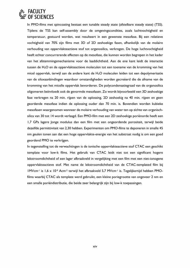
Bornside et al.[44,45] divide the spin-coating into four stages: deposition, spin-up, spin-off and
evaporation, although for sol-gel coating, evaporation normally overlaps the other stages (Figure
1.9). In the deposition stage, a solution is deposited on the substrate. Then, at the spin-up stage,
the substrate is accelerated to the desired rotation rate and the liquid flows radially, owing to
the action of centrifugal force. In the spin-off stage, the excess liquid is ejected off the edge of
the substrate. The film continues to thin slowly until disjoining pressure effects cause the film to
reach an equilibrium thickness or until it turns solid-like due to a dramatic rise in viscosity from
solvent evaporation. In the final stage, the thinning of the film is due solely to solvent evaporation.
A model first proposed by Meyerhofer[46] has been found to capture much of the essential
characteristics of the spin coating process even though it decouples evaporation and flow. This
model captures the experimentally observed scaling of the final thickness hf ∼ 𝜂013⁄ 𝜔−1 2⁄ , where
η 0 is the initial solution viscosity, and ω is the final rotation speed.[47] After spinning, the sol
undergoes a sharp increase in viscosity and transforms into a ‘‘wet gel.’’ The wet gel is a
somewhat rigid substance yet consisting of a liquid and a solid component. The solid part is
formed by a three dimensional network of linked polymers spanning throughout the film, while
the liquid fills the free space surrounding the solid part. As the film dries, it shrinks in volume.
Once the film is attached to the substrate and unable to shrink in that direction, the reduction
in volume is accommodated completely by a reduction in thickness. When the film has solidified
and stresses can no longer be relieved by flow, tensile stresses develop in the plane of the
substrate. It is commonly observed that cracking of films does not occur if the film thickness is
below a certain critical thickness hc ≈ 0.5-1 μm.[48] Subsequently, the gel is dried by a thermal
step at a moderate temperature (bake). During the bake step, the original solvents are removed
and the film undergoes a major weight and volume loss of up to 50%. Based on the technique
used for drying, a distinction between xerogels and aerogels can be made.[49] Xerogels are
formed through conventional drying by evaporation, while aerogels use supercritical drying of
solvents. Finally, a sintering at temperatures varying from 350 to 600°C (cure) is required to
Figure 1.9. Spin-on deposition sequence consisted of 1) Dispensing sol on a substrate; 2) Spin-up; 3) Spin-off; 4) Evaporation

14
obtain a stable film. The cure step induces the final cross-linking of the polymer chains and results
in a mechanically stable film structure.
During the spin-coating process, the evaporation of solvent takes place at the top surface of the
flowing fluid, thus a concentration profile for the solute species will exist within the flowing
solution. Since the solute species in sol-gel solutions undergo polycondensation reactions, it is
possible for the top surface to experience a rapid increase in viscosity and potentially to act as
a barrier to further evaporation. It has been shown that the evaporation rate applicable through
the entire first stage of spin coating is nearly the same as that for pure solvent.[50] Thus the top
surface composition does not deviate greatly from its starting value until very near the end of
coating formation process, when flow has effectively ceased and the coating drying stage
begins.[50] Solvent evaporation leads to localized surface tension gradients which in turn drive a
non-uniform film distribution at the surface. It has been demonstrated that the evaporation of
solvents from the spin-on solution has significant impact upon the development of striations in
spin-on films. The striation defect appears as radially oriented regions of thicker film that often
develop in a corrugated, spoke-like profile across the surface of spin-on films. The primary
driving force behind striation growth is capillary induced lateral fluid migration at the
fluid/atmosphere interface.[51–54] This thin film spreading due to surface tension imbalance is most
commonly referred to as the “Marangoni effect”.[55] A decrease in height and an increase in
spacing of the striations have been observed when alcohols of high boiling points are used.[56]
Another strategy to minimize the striations has been to employ a mixture of solvents in which
the more volatile solvent possesses higher surface tension with the air.[57]
In contrast to the PECVD, for spin-on materials, the basic structure and bonding arrangement
of the initial material are usually maintained to a large degree in the product. Spin-on
organosilicate materials are usually prepared by sol–gel processing. This method is generally
associated with the preparation of glasses or ceramic materials derived from metal alkoxides.[49]
Sols are dispersions of solid, colloidal particles (1–100 nm in diameter) in a liquid resulting from
the initial hydrolysis and condensation of silica precursors. The sol represents the processable
state of these materials. Gels, on the other hand, are interconnected rigid network structures
characterized by the lack of tractability and solubility. Thus, silica gels may be produced from the
growth of discrete colloidal particles or by the simultaneous hydrolysis and condensation of a
suitable precursor, generally an alkoxysilane. The latter approach does not need to exhibit a
distinct colloidal stage and condensation is preferably, temporarily arrested while still in the
soluble stage. The typical preparation of these materials by the sol–gel process involves the
hydrolysis and polycondensation of alkoxy- and/or halogenated silanes in the presence of water
and a suitable catalyst. The catalyst is typically a mineral acid (HCl, HNO3, etc.), which promotes
the hydrolysis reaction to yield silanols. On the other hand, basic catalysts tend to favor the

15
polycondensation reaction. The silanol functionality readily reacts with itself or an alkoxy/chloro
group in a condensation step, which forms siloxane groups and eliminates water or alcohol/HCl.
In this fashion, a highly cross-linked network is ultimately formed. The sol–gel approach is subject
to many variables, such as the nature of the catalyst, the amount of water relative to alkoxide
groups and the reaction temperature. These will be discussed more in detail in the section
dedicated on the spin-on silsesquioxane-based low-k candidates.
1.5. Low-k candidates
As the IC industry is interested in implementing dielectric materials with ultra-low k value, i.e.
k<2.4, in this section, we will consider the low-k candidates with a dielectric constant lower
than 2.4 which have received the most attention. We will consider their appealing properties
and the issues which need to be resolved before they can be integrated as an inter-layer
dielectric. The introduction of porosity in organic and ceramic materials is ubiquitous throughout
the literature as the only viable method to obtain ultra-low-k materials. A distinguishing feature
here is that the porosity for dielectric applications must be nano-sized, should be evenly
distributed, must be produced under typical BEOL conditions and must be generated in thin
films. As compared to interconnected pores, the presence of isolated pores is more compatible
with integration demands, even if this is hard to achieve at pore volumes above 25% usually
required to achieve an ultra-low k value.
Candidates k @
100 kHz
YM
(GPa) �̅�, nm Breakdown
field,
MV/cm
Thermal
stability,
°C
CTE,
ppm/K
SiO2 3.70-4.50 55-74 - >10 >1500 0.5
HSSQ 1.85-2.80 <2-8.3 <1-3.5 <5 <350 20
MSSQ 2.0-2.80 3.8-4.5 3.5 ~5 ~550 80-110
Aerogels 1.03-2.10 <2 5-20 <0.5 Unstable High
Xerogels 1.70-2.30 <4 <1.5-30 0.5-2 ~450 62.2
Zeolites 1.70-3.10 7-54 <1-70 <3 >1000 57.4-71.7
PMS 1.5-2.6 1.5-14.4 3.4-9.0 3-4 >450 ?
CDO 1.95-2.80 4-8.5 2-4 5-6 >450 12
PMO 1.7-2.9 1.86-20 2-4 >5 >450 10
Polymers 2.2-2.80 2.45 <1-15 4 300-500 40-100
MOF 1.2-4.8 4.7-8.6 <1-? ? ~450 -75-11.7
BC:H >2.6 126 - <2 ~1500 Low?
Table 1.1. Overview of the low-k properties of the low-k candidates described in this chapter.

16
1.5.1. Silicates and zeolites
1.5.1.1. Hydrogen silsesquioxane (HSSQ)
One of the earliest and most extensively studied silicates targeted for dielectric applications was
hydrogen silsesquioxane (HSSQ). HSSQ is an analogue of SiO2 where one of the four oxygen
atoms bonded to Si has been replaced with a hydrogen atom.[15] Thus, the empirical structure is
generally designated as (HSiO1.5)n or (HSiO1.5)2n (n = 2, 3...) in order to indicate the polyhedral
nature of the precursor oligomers. In the HSSQ materials, the Si and O atoms are arranged in
the form of a cage or a ladder (Figure 1.10).[58] The cage can include eight (T8), ten (T10), twelve
(T12) or more silicon atoms. The cages in polymerized HSSQ are connected to each other
through oxygen atoms while other cage corners are terminated by hydrogen. The cage structure
creates free volume, decreasing the material’s density and, therefore, its k value. For coatings
cured to the thermal limit of 400°C in inert ambient, the dielectric constant of HSSQ is
approximately 2.8 with a Young’s modulus of 8.3 GPa and a tensile stress of approximately 70
MPa.[59] On the other hand, porogen-based HSSQ have been reported to reach a dielectric
constant as low as 1.85 at a 50% porosity and a pore size of 3.5 nm.[60] Additionally, the films
have low stress values, 20 ± 5 MPa. The films are also sensitive to an exposure to oxidizing
plasmas during the deposition of a sealing layer resulting in an increase of the dielectric constant
with time. While a sealing layer containing no oxygen, such as the SiC:H is shown to have no
detrimental effect on the low-k properties, the large pore size required the deposition of at least
25 nm thick sealing layer due to a significant penetration into the pores.[61]
One of the issues encountered with HSSQ materials is their thermal stability.[62] At temperatures
between 250 and 350°C, the cage-like structure transforms into a more randomly cross-linked
network structure. At temperatures higher than 350 °C, the evolution of SiH4 and H2 is
observed. At temperatures ranging from 350 to 400 °C, the HSSQ film expands, while from 400
to 450 °C, it contracts.[63] Consistently, the refractive index and the dielectric constant first
decrease due to formation of free pore volume and then increase due to densification.[64] On
the other hand, a steady increase of the dielectric constant with the temperature has also been
Figure 1.10. Structures of silsesquioxanes
17
reported,[62] possibly, showing the dependence of the HSSQ response on the distribution of the
cage sizes, information which is not always available when proprietary low-k films are evaluated.
Another issue preventing the integration of the HSSQ films is their chemical stability.[15] When
exposed to oxidizing plasmas, utilized for photoresist striping, the HSSQ readily oxidizes and
forms silanols upon subsequent exposure to ambient moisture. This leads to increased leakage
current and offers a pathway for fast environmental stress cracking.[65]
1.5.1.2. Aerogels
Aerogels are sol-gel derived materials with extremely high porosities of up to 95%, large open
pores, and a high internal surface area which may exceed 1000 m2/g.[49] The large pore volume
is made possible due to a procedure which allows the removal of the pore fluid from wet gels
minimizing the capillary forces during the drying stage. One of the most often employed drying
method is the supercritical drying that minimizes the capillary forces and conserves the pore
structure of the wet gels with a minimal shrinkage. In one of the first studies, the dielectric
constant of a 3.4 µm thick silica aerogel was reported to be 1.79 (78% porosity).[66] Nevertheless,
due to the presence of residual silanols after the supercritical drying, water is adsorbed inside
the pores resulting in an increase of the dielectric constant and the leakage current.[67] If the
aerogel is consequently annealed at 450°C, a lower dielectric constant (k=2.0) and leakage
current (J = 10-5 A/cm2 at 1 MV/cm) are obtained as compared to the as-synthesized material (k
= 2.1, J = 10-4 A/cm2 at 1 MV/cm).[68] A similar effect, 12% lower k-value and almost 2 orders of
magnitude lower leakage current, is observed after silylation using trimethylchlorosilane.[69]
While ultralow-k aerogel films can be successfully prepared, the processing conditions are not
easily adaptable to continuous thin-film-forming operations and would lead to higher production
costs. In terms of material properties, the big pores (10-20 nm), the extremely poor mechanical
properties, and the hydrophilicity, if no silylation is performed, make the aerogels challenging to
integrate in the back-end-of-line of microchips.[15]
1.5.1.3. Xerogels
The preparation of xerogels employs a drying procedure which does not require supercritical
conditions resulting in lower pore volume than aerogels. Therefore, xerogels have lower
production costs and better mechanical properties making them more interesting for a low-k
application. There are two main procedures for the preparation of xerogels – a two-step acid-
catalyzed scheme and a two-step acid-base-catalyzed scheme. Due to the low condensation rate
associated with the two-step acid-catalyzed procedure, the solvent removal from the gel results
in a significant shrinkage leading to a monolith/film with a very fine texture where about 65% of
the pores have a radius smaller than 1.5 nm.[70] On the other hand, the higher condensation rate
at the second step of the acid-base-catalyzed procedure leads to more highly branched oligomers

18
preventing interpenetration and therefore during the solvent removal, the shrinkage stops at an
earlier stage due to the stiffness of the impinging clusters. This results in larger pores, so that
the maximum capillary pressure is reduced compared to the previous example. This xerogel has
less microporosity and a broader distribution of larger pores.[70] An important final step is the
immersion of the film in a nonpolar solvent, e.g., n-hexane, to allow the replacement of ethanol
and subsequent surface modification with a silylation agent such as hexamethyldisilazane (HMDS)
or trimethylchlorosilane (TMCS). Capping the reactive hydroxyl groups in the ambient drying
process makes the shrinkage upon drying reversible since the organosilyl-functionalized pore
surfaces cannot participate anymore in the condensation reaction or hydrogen bonding when
the gel collapses due to the capillary tension developed during drying; therefore, the shrunken
network elastically springs back to its original porous state. The silylation of xerogel films is
important to maintain a high porous volume and is also beneficial for the dielectric constant
through removal of polar Si-OH groups.[15,21] The two-step acid-base-catalyzed procedure
results in films with significantly higher pore volumes and has therefore received more attention
from the IC industry. The relationship between the structure of the gel and xerogel is shown
schematically in Figure 1.11.
Using the acid-base-catalyzed procedure, films with porosities between 45 to 90% and dielectric
constants at optical frequencies between 2.5 and 1.14 have been reported.[71,72] The aging time
can be used to tailor the porosity of the xerogel films since dissolution and re-precipitation
reactions cause neck formation between the particles. The time and temperature of the aging,
the pH of the medium, and the solvent influence these reactions. The porosity first increases
with time, reaches a maximum, and then decreases.[73] The aging time also affects the fracture
toughness of xerogel films and there may be an optimal aging time and temperature for maximum
fracture toughness.[74] The contact angle of water on the xerogel films annealed in forming gas
at 450°C for 30 min is 100°. The anneal in forming gas significantly reduces the leakage current
measured at 1MV from 3.21 × 10⁻⁵ A/cm-2 (before anneal) to 6-8 × 10⁻⁶ A/cm-2 (after anneal).[75]
The stress of a 50% porosity xerogel film is below the detection limit (38.6 MPa) and the stress
Figure 1.11. Structural relationship between the sol, gel and the final
aerogel/xerogel[49]

19
of the sample after 450°C annealing (60% porosity) is 40.5 MPa.[72] Silica xerogel films display
relatively low dielectric strength with a breakdown field close to 2 MV/cm.[71]
Because control of the solvent evaporation is not always easy, another approach has been
developed where a nonvolatile co-solvent (ethylene glycol) is added to the sol, allowing spin-
coating in an open, ambient atmosphere.[76] Compared to the controlled evaporation process,
porosity is now determined by the ethylene glycol/TEOS volume ratio. In this case, a narrower
pore size distribution is obtained as compared to the film made with only ethanol as a solvent,
resulting in higher hardness and modulus.[77] Nevertheless, the average pore size increases
exponentially with increasing porosity.[76] The Young’s modulus has been found to have a power
law dependence on the porosity in the range between 25 and 75%.[77]
While low dielectric constants can be obtained in the case of xerogels, control of the pore size
is difficult and the processing conditions are not always compatible with mainstream
manufacturing. The reported pore sizes between 10 and 30 nm[78,79] make the integration of
these materials and improved formulations in a real structure extremely challenging.[15] Another
issue is related to the low Young’s modulus of E<4 GPa[80] while a minimum value of 4 GPa has
been reported to be required if a low-k dielectric is to survive the chemical mechanical polishing
(CMP) step.[81] Additionally, the film is also significantly damaged during the photoresist strip. If
an integration scheme is designed in order to prevent the interaction of the plasma reactive
species with the xerogel material then an improvement of the breakdown voltage has been
observed.[82]
1.5.1.4. Zeolites
Zeolites are microporous crystalline materials that consist of open aluminosilicate frameworks
derived from [SiO4]4− and [AlO4]5− tetrahedra linked to form cages, channels or cavities of
various sizes.[83] In contrast to the classical aluminosilicate zeolites, the pure silica-zeolites (PSZ)
consist of only silica tetrahedra and therefore do not contain framework charges or cations that
would be detrimental for electronic applications. The PSZs which have received most attention
from the IC industry for low-k application are silicalite-1[84] and silicalite-2[85] (Figure 1.12). Due
Figure 1.12. Structures viewed along [100] of a) MFI and b) MEL framework types to which the Silicalite and
Silicalite-2 pure silica zeolites (PSZ) belong
a) b)

20
to their microporous crystalline structure, better mechanical properties as well as reduced
barrier and/or metal in-diffusion are expected.[16] Indeed, a nanoindentation investigation of a
single PSZ FER crystal provided evidence for a significantly superior elastic modulus as compared
to amorphous silica at a given density reporting an experimental YM of 49.4 GPa and a calculated
k of 1.78.[86]
Two main strategies have been employed for the preparation of PSZ films:[86,87] 1) in situ
crystallization in an autoclave of a solution composed of tetrapropylammonium hydroxide
(TPAOH), tetraethoxysilane (TEOS) and water, and 2) spin-coating of a solution containing
silicalite nanocrystals. The porosity in the zeolite films originates from the intra-particle porosity
within the zeolite nanoparticles and the inter-particle porosity owing to the packing of the near-
spherical nanoparticles in thin film morphology. In order to produce films with a reasonable
quality, good particle size monodispersity is required.
In-situ crystallized films possess excellent mechanical properties with YM=30–40 GPa for
dielectric constants ranging from 2.7 to 3.1.[16] Impressive low-k properties, k=1.7 and YM=54
GPa, have been reported for an MFI PSZ obtained following a low temperature synthesis in
combination with a non-thermal photochemical activation.[88] The k and the YM are close to the
theoretically predicted values for the single-crystal MFI. The hydrophilicity and the dielectric
constant of the films has been shown to decrease with the increase of the water in the starting
mixture.[89] Nevertheless, a significant increase in leakage current has been observed. It has
additionally been shown that the in situ crystallized film’s hydrophilicity increases with exposure
to water vapor.[90]
On the other hand, silicalite spin-on films present lower dielectric constants (k = 1.8–2.1) due
to the additional porosity gained from inter-nanocrystal packing voids.[87] By increasing the
Silicalite-1 nanocrystals content, the crystallinity, hydrophobicity, roughness and porosity
increase while YM and dielectric constant decrease. Additionally, a better cohesion is observed
for films with a lower nanocrystal content due to the absence of large interstitial voids between
the nanoparticles which in films with higher nanocrystal content often result in cracks.[91] The
presence of larger mesopores also affects the adhesive properties of these films, leading to failure
during CMP.[92] The pore size evolves with crystallization time. A crystallization time of up to 4
days results in micropores of 0.55 nm and 2-5 nm mesopores while a longer crystallization leads
to pores with a size of tens of nanometers.[91,93] While the films with lower nanocrystal content
possess better cohesion, they are hydrophilic which has a detrimental effect on the k value which
increases from 2.1 to 4 within minutes.[94] This has been resolved by silylation treatments. A
silylation with TMCTS results in a film with an elastic modulus of 7.03 GPa and a dielectric
constant of 1.94 for which the mean-time-to-failure lifetime of time-dependent dielectric
breakdown has been estimated to be longer than ten years at 125°C under the electric field of

21
3.4 MV/cm.[95] Additionally, the dielectric constant and the leakage current become lower as the
synthesis temperature increases.[95] The silylation results in a YM as high as 18 GPa for a
dielectric constant at an optical frequency of 2.1.[94] Nevertheless, the silylation decreases the
porosity. The incorporation of trimethylsilyl (TMS) groups decreases the porosity by 26-56%,
depending on the initial pore size distribution. The smaller the pores, the larger is the impact of
the incorporation of TMS groups.[96] Furthermore, a combination of UV cure and silylation
treatments have been employed in order to improve the low-k properties. A calcination,
followed by a silylation, a UV cure with λ=254 nm and another silylation with TMCTS results in
a PSZ film with a YM of 10 GPa and k value of 2.18.[97] On the other hand, a UV cure with a
λ=172 nm combined with a silylation with TMCTS results in MEL-type PSZ films with a YM=5.7,
k=1.9, and a leakage current density of 10-9 A/cm2 at 2MV/cm.[98] Unexpectedly, a UV cure
(λ=200-400 nm) at 425 °C hydrophobizes spin-on Silicalite-1 films by grafting the silanols with
the organic template. Moreover, the silanol condensation enhances the fusion of the grains,
minimizing the intergrain voids and as a result the mesopore size decreases from larger than 50
nm to 2-8 nm. The film has a dielectric constant of 2.16 and an elastic modulus of 10.7 GPa.[99]
In order to achieve a k value in an even lower range, additional mesoporosity has been
introduced by the incorporation of organic labile molecules in the zeolite suspension. For
instance, the inclusion of 5–15 wt % of cyclodextrin in the synthesis procedure leads to a
controllable interparticle pore size ranging from 2.71 to 3.29 nm.[100] A k value of 1.8 is obtained
for a 15 wt % porogen loading, while the mechanical properties for this film remain excellent,
YM = 14.3 GPa. When the surfactant Tween 80 is included in the suspension, the resulting films
have uniform and smooth surfaces, an average mesopore size of 4.5 nm, a k values <2, low
leakage current density (i.e., 6×10⁻⁹ A/cm2), and an elastic modulus of 13.4 GPa.[101] Furthermore,
the surfactant Pluronic F127 has been employed to obtain films with porosities between 9 and
60% and k values between 2.9 and 1.9 while the elastic moduli are in the range of 13-20 GPa.[102]
Importantly, the addition of methyl triethoxysilane to the deposition solution results in
hydrophobic films which do not require a post-silylation treatment and the k value does not
change after exposure to air with a relative humidity of 40-60%. Nevertheless, this approach
retards the crystal growth of the zeolites.[102]
Organic-inorganic hybrid zeolite materials have not yet received attention from the IC industry
but their organic framework might be beneficial for their chemical and electrical stability.[103] In
organic-inorganic hybrid zeolite materials some of the oxygen atoms are replaced by a methylene
group. The use of methylene-bridged organosilane as a silicon source gives zeolite materials
containing an organic group as lattice, with several zeolitic phases such as the MFI and the LTA
structures. The material is not a physical mixture of conventional zeolite and amorphous organic-
containing material but contains a genuine organic-inorganic hybrid zeolite. Some of the

22
methylene frameworks (Si-CH2-Si) are partly cleaved to give rise to methyl groups[103] which is
expected to hydrophobize the zeolites making them more suitable for low-k application.
Recently, Poloni et al. performed DFT simulations in order to screen for the most promising
low-k candidates among the known and some hypothetical pure-silica zeolites. They recommend
six zeolites within the IZA database (JSR, IRR, OBW, BOZ, OSO, and NPT) exhibiting both
ultra-low-k (2.27, 2.33, 2.34, 2.37, 2.39, and 2.49, respectively) and relatively large bulk modulus
(47.0, 42.1, 65.1, 57.6, 64.6, and 72.9 GPa, respectively).[104]
In spite of the impressive k and YM values reported (Figure 1.13), zeolite films suffer from a
variety of problems arising from the particulate nature and the unwanted large, non-ordered
mesoporosity caused by irregular nanoparticle shapes. Particle size of the crystallites may also
be a problem as feature size dimensions approach 10 nm and below. Non-uniformities within
films results in poor etch rates or variations and difficulties at CMP steps.[105] The films have high
surface roughness that is difficult to reduce as polishing will generally result in pull-out of
individual nanoparticles. Furthermore, the interparticle voids will also become problematic
during the patterning of the dielectric layers and also at the seeding barrier layer integration
steps.[105] For these reasons, the use of silicalite films as low-k materials in semiconductor
manufacturing currently does not seem realistic.[16]
1.5.2. Polymers
Organic polymers have been receiving a decreasing interest from the low-k community judged
by the way they have been presented in the last 15 years in the comprehensive reviews on the
advances in the low-k research.[13,15,16,20] Organic polymers can be divided into two different
groups with respect to their dielectric response: non-polar (low-loss) and polar polymers. Non-
polar polymers contain molecules with almost purely covalent bonds. Low-loss polymers have
Figure 1.13. Comparison of the YM and the k-values of the reported zeolite films.[88] Color code
for zeolite type—Blue: MFI, Red: MEL, Black: FER, Green: BEA, Orange: CHA, Yellow: LTA.
[86] [86] [86] [86] [211] [212] [213] [94] [214] [215] [216] [100] [217] [217] [88]

23
dielectric constants which are independent of frequency. On the other hand, polar polymers
contain heteroatoms which contain different electronegativity giving rise to an asymmetric
charge distribution. Therefore, polar polymers have higher dielectric constant which is frequency
dependent. While saturated hydrocarbons have a lower polarizability than unsaturated,
conjugated and aromatic hydrocarbons, the aliphatic C-C, C-H, and C-N bonds are generally
not stable at T≥300-400°C. The polymers with a sufficient thermal stability (450-500°C) usually
contain aromatic, cross-linked or ladder structures. The thermal stability can also be improved
by fluorination which additionally decreases the dielectric constant. Nevertheless, most of the
organic low-k films with sufficient thermal stability have dielectric constants close to 2.6-2.8.[20]
Therefore, the applicability of majority of the organic polymers for low-k is limited because of
their low thermal stability, softness and high CTE. The large CTE of polymers, on the order of
40-100 ppm/K,[15] is unsuitable since repeated thermal cycling causes a stress buildup due to the
thermal mismatches with the neighboring materials which can lead to delamination and adhesive
failure.
One class of organic polymers that have acceptable thermal stability are polyarylene materials
(Figure 1.14). These materials are marketed under the trade name of SiLKTM. These materials
have been reported to have Tg values in excess of 450°C with a dense dielectric constant of 2.65
and excellent thermal stabilities.[106] Therefore, in order to meet the needs for the 10 nm
technology node and beyond of a dielectric with k<2.4, the SiLK needs to be made porous.
Nevertheless, the low k value of the dense SiLK means that a lower pore volume will need to
be introduced as compared to silica in order to reach a k<2.4. The SiLK needs to be annealed
at a T>325°C before it acquires high enough elastic modulus to prevent a collapse of the material
due to capillary pressures during the porogen decomposition.[15] As a result, the porogen needs
to have a decomposition temperature higher than 325°C. Polystyrene has been employed as a
porogen together with the B-staged1 SiLK resin resulting in a film with a mean pore size of ∼40
1 B-staging refers to the partial cure (i.e. oligomerization) of the polymer[107]
Figure 1.14. The polymerization reaction leading to the SiLK

24
nm and dielectric constants in the 2.2-2.3 range.[107] A polyarylene film with a dielectric constant
below 2.0 has been reported to have a bimodal pore size distribution centered around 5 Å and
80 Å.[108,109] A k ∼ 2.2 can be achieved by a thermally initiated graft of polyethyleneglycol
methacrylate onto a SiLK film resulting in pore sizes in 10-15 nm range.[110] It is clear that pore
sizes in this range are unsuitable for integration into the 10 nm and beyond. Nevertheless, the
average pore size has been decreased to <2 nm while also improving the CTE from ∼ 65 to ∼45
ppm in the SiLK Y formulation.[15] The porous SiLK is the only porous organic material for which
integration studies have been reported, both single and dual damascene but it has not been
employed in a large scale manufacturing.[15]
1.5.3. Organosilicates
This section considers the main low-k candidates for future generation technology nodes, the
organosilicates. We have divided the organosilicate low-k films into three categories: 1) porous
SiCHO (pSiCHO) dielectrics obtained from a PECVD process; 2) spin-coated
methylsilsesquioxane (MSSQ) materials and their derivatives; 3) spin-coated and PECVD
oxycarbosilanes (OCS). The pSiCHO are the dielectrics employed so far in chip manufacturing
which makes them the most seriously considered low-k candidates. The interest towards the
MSSQs have diminished due to their insufficient mechanical properties and therefore we will
also consider their derivatives with improved mechanical stability. Finally, the OCS films contain
bridging alkylene groups (Si(CH2)nSi) which allow the introduction of carbon in the low-k matrix
without having a detrimental effect on the matrix connectivity and the Young’s modulus.
1.5.3.1. PECVD pSiCHO dielectrics
The PECVD porous SiCHO films can be generated either by using a precursor containing a
functional group that will generate a second phase during deposition or by mixing a matrix
precursor with a reactive hydrocarbon molecule, also called a porogen. Typical precursors
selected for the former approach are vinylmethylsilanes. For precursors containing more than
one vinyl group per silicon, the organic phase formed during deposition becomes less volatile
due to a higher degree of cross-linking.[111] While dielectric constants as low as 2.0 can be
obtained with vinyltrimethylsilane, no convincing integration results have been presented.[15]
On the other hand, the porogen (subtractive) approach is the more versatile way to obtain
pSiCHO films.[38] In the first step of the porogen approach, matrix and porogen precursors are
transformed into species that eventually lead to the formation of a ‘hybrid’ film composed of an
organosilicate matrix enclosing organic inclusions. The porogens need to have some weak bonds
that are easily dissociated in the low-power plasma such as unsaturated cyclic hydrocarbons like
terpinenes or norborenes; linear alkenes; or molecules with strained rings like cycloalkene
oxides or butadiene monoxide.[38] In the second step of the porogen approach, the porogen

25
molecule fragments are removed. At this point, the film usually becomes porous and has low-k
properties.[28] The removal of the porogen can be done by annealing the films at ca. 400°C in an
inert ambient, or using electron beam (e-beam) or UV irradiation. The latter two techniques are
much faster than the thermal anneal, can enhance the matrix cross-linking and improve the
mechanical properties of the pSiCHO films.[112,113] Additional ways to remove the porogen
include H2 plasma and supercritical CO2.[114,115]
The most often used curing approach in research labs, is the thermal anneal. However, the
thermal anneal of 4 h at 400°C in He[116,117] is usually insufficient to remove completely the
porogen. An anneal at a temperature higher than 430°C is not suitable since this is the upper
limit for an integration with Cu metallization. That is why the e-beam cure and the UV cure have
been investigated. Both types of cure are done at temperatures of ∼400°C for durations of
minutes. Both e-beam and UV cure remove porogen from the deposited films but can also
remove some skeleton bonds such as Si-CH3, Si-H, and Si-OH, leading to the formation of new
Si-O-Si cross-links. E-beam cure is performed with electrons at energies of ∼2 to ∼10 keV, the
energy of the beam needed for curing scales with film thickness.[112,118] The e-beam can induce
damage in the active devices during integration processing.[38] The degree of damage induced by
the e-beam cure increases with the thickness of the gate oxide and with the dose of the e-beam
and is more likely to occur at higher electron energies.
As a result, the UV cure is the preferred technique for curing pSiCHO films. In order to elucidate
the effect of the photon energy during the UV cure, some authors have used monochromatic
UV light,[119,120] while in high volume manufacturing, UV cure is performed by the use of
broadband UV lamps.[38] During UV irradiation, the porosity is created through a combination
Figure 1.15. Bond dissociation energies of different structures in the SiOCH material[28]

26
of the photonic breaking effect (Figure 1.15) and thermally activated degradation of porogen.
Thanks to this double effect, the porogen is removed from the film within a few minutes.[28] The
initial porogen removal makes the film porous resulting in a decrease in Young’s modulus as
compared to the as-deposited film. A continued exposure to UV causes a densification of the
film resulting in increase in modulus owing to an enhanced cross-linking.[38] This densification is
a result of the breaking of Si-CH3 bonds and rearrangement of the skeleton by increased cross-
linking. The lowest achievable dielectric constant in pSiCOH films depends on both the porogen
and the matrix precursor. For instance, at high fractions of porogen incorporated in the as-
deposited films, the removal of the porogen may result in a collapse of the thickness rather than
in enhancing porosity. As a result, the dielectric constant does not decrease with increasing the
relative amount of porogen beyond the value corresponding to the minimum k.[117] On the other
hand, if the matrix of the as-deposited film is strong enough, ultra-low-k films with k=2.1 can be
achieved by increasing the relative amount of the porogen.[117] In the latter case, the shrinkage
reaches a plateau and therefore the increase of the porogen content results in continuous
increase in the porosity of the film and corresponding decrease in its dielectric constant.[13] In
order for the matrix to be mechanically strong enough to avoid collapse after the removal of
the porogen, it should be minimally bonded to the porogen species to avoid forming dangling
bonds or other defect sites.[121] In terms of structure, the SiCHO constituted by silicon bonded
to more than one methyl group are not able to prevent significant film shrinkage. This behavior
has been discussed using percolation of rigidity arguments.[25] Networks below the percolation
threshold are more deformable than those above the percolation point and the maximization of
O3-Si- and O4-Si- units is necessary to avoid the film collapse.[28]
The increase of the C content from 0 to 19 at.% in pSiCHO films leads to a decrease in the ionic
contribution to the dielectric constant from 1.86 to 0.25 and a much smaller reduction of the
electronic contribution from 2.10 to 1.90.[122] The dipolar contribution becomes negligible as the
C content increases. Therefore, the reduction of the ionic contribution, owing to the decreases
in the film density and in the number of Si-O groups in the films, is the predominant factor in
the reduction of the overall dielectric constant.[122] Furthermore, porous SiCHO films with low
leakage currents of less than 10-8 A/cm2 at fields below 2 MV/cm1 have been reported making
them suitable for integration in a chip interconnect.[38] The porous SiCHO dielectrics have
intrinsic tensile stresses in the range of 35 MPa to 55 MPa depending on the deposition and
curing conditions. The stress values increase with UV cure time and, for the same chemistry,
will normally be smaller for films of lower k and corresponding lower E values.[38] One factor
which determines the strain and stress in the low-k during the thermal cycling in the integration
process is the CTE. The reported CTE values of ∼12 ppm/°C for pSiCHO with k = 2.1[117] are
suitable since they are similar to that of copper. Interestingly, no correlation of pore size with

27
the molecular volume of the porogen has been established. The pores seem to be formed by a
species larger than one porogen precursor molecule, which could be created either in the plasma
phase, on the film surface or even in the bulk of the film during the curing stage.[37] Nevertheless,
even though the porogen nature seems not to determine the pore size in a simple way, it has
an impact on the film properties because it modifies the structure of the produced organosilicate
network.[37] For example, when a deuterated porogen is used with DEMS, extensive hydrogen
and deuterium scrambling is observed between the porogen and the inorganic network.[123]
Furthermore, it is a common observation that with the increase in the pore volume of pSiCHO
films, the pore size increases making them unacceptably large when porosity values of 40% or
higher are achieved.[124,125]
Dense SiCHO films prepared from cyclic siloxane precursors possess superior mechanical
properties to those prepared from linear methylsilanes.[13] Nevertheless, it is difficult to
incorporate porogen in films deposited with cyclic matrix precursors, such as TMCTS or
octamethylcyclotetrasiloxane (OMCTS), and large porogen to skeleton flow ratios have to be
used to fabricate pSiCOH films.[126] Lower flow ratios have to be used with non-cyclic skeleton
precursors, such as the branched DEMS.[38] Additionally, an efficient incorporation of the CxHy
porogen fractions in the deposited films requires the use of porogen molecules with at least two
reactive bonds, such as double C=C bonds or strained bonds such as in the bicycloheptadiene
or a-terpinene.[30,127] Nevertheless, the presence of such bonds in the porous film[112,128] has been
linked to a deterioration of the electrical reliability.[129] Even if the presence of sp2-carbon in the
pSiCHO films is not considered to be the result of the use of porogens with double bonds,[112]
it has not been ruled out. Rather, such structures are thought to arise from the degradation of
the porogen under energetic conditions in the plasma, this signal being observed in the hybrid
film and not in a matrix film.[112] These types of graphitic-like residues are not observed in spin-
on films after UV curing.[130] The presence of porogen residues leads to an increase of the
electronic and dipolar contribution of the permittivity.[28] These structures hold a permanent
dipolar moment and non-localized valence electrons. Moreover, these graphitic-like structures
are more conductive than the SiCHO skeleton and as a result, a correlation between porogen
residue and leakage current has been shown.[29] The breakdown field is also affected by the
presence of these residues. When a H2 plasma treatment is combined with a UV cure, a pSiCHO
film with undetectable porogen residues is obtained.[131] The limitation of this approach is that
the film must be thinner than 200 nm. Otherwise, hydrogen treatment can densify the top layer,
which induces inhomogeneity and prevents the porogen extraction.[28]
1.5.3.2. Methyl Silsesquioxanes (MSSQ)
Silsesquioxanes are polymers with the empirical formula (R–SiO3/2)n . These compounds derive
their name from the one-half (3/2) or sesquistoichiometry of oxygen bound to silicon. In

28
particular, the methyl silsesquioxanes (MSSQs) are analogous to the orthosilicate structure,
where one of the four oxygen atoms bonded to silicon has been replaced by a methyl group.
The most common representatives are a ladder-type structure, and a cage structure containing
eight silicon atoms placed at the vertices of a cube (T8 cube).[20] MSSQs are prepared by a sol-
gel chemistry. Here, we will consider the MSSQ polymeric films reported from
methyltrialkoxysilanes and their copolymers with the tetraalkoxysilanes with a dielectric
constant below 2.4.
Compared to the HSSQ films, MSSQ-based films show better thermo-oxidative stability. Under
inert atmosphere, MSSQ demonstrates high thermal stability of ∼550°C and low oxygen
sensitivity to 300-350°C.[15] “Dense” MSSQ films have a dielectric constant of 2.7-2.8 and
breakdown field higher than 4 MV/cm. The low dielectric constant is a result of the low
electronic polarizability of the methyl substituent along with the presence of constitutive
porosity estimated to be 6.7%.[15] Relatively low YM values, ranging from 3.8 to 4.5 GPa, have
been reported while the CTE tends to be fairly high, in the range of 80-110 ppm/°C, compared
to SiO2 with a CTE of approximately 0.50 ppm/°C.[132]
The presence of Si-Me groups in the MSSQ, while necessary to achieve lower k, disrupts the
connectivity of the silicate network and deteriorates the film mechanical properties. Therefore,
in order to increase the network connectivity, copolymers derived from MSSQ with other
monomers have been explored. For instance, porous films have been deposited from
methyltrimethoxysilane (MTMS) and TEOS with molar ratios from 0 to 9 and
cetyltrimethylammonium bromide (CTAB) as the porogen.[133] Films with 60% porosity could be
obtained without pore collapse. In order to ensure the hydrophobicity of the films, the MTMS
needs to be at least 50 mol% in TEOS. Furthermore, at a constant porogen loading, the dielectric
constant decreases when the ratio of MTMS in TEOS increases. Surprisingly, partial crystallinity
in the matrix of the mesoporous films could be observed, although the mechanism of
crystallization could not be established. The small pore diameter of only 3 nm at 50% porosity
is an advantage for low-k application and cannot be achieved by a PECVD method.[134] Small pore
size of up to 3.5 nm at porosities higher than 50% can be obtained by various
tetraalkylammonium bromide porogens.[135] Additionally, a YM of ca. 4 GPa, sufficient to survive
a CMP step, for a film with a k of 2.0 has been demonstrated.[135]
Interestingly, there seem to be no systematic studies which have evaluated the impact of the
MSSQ synthesis conditions on the low-k properties even if the hydrolysis and condensation of
alkoxysilicates have been extensively researched and it has been shown that different oligomers
and polymers are obtained depending on the pH and the H2O:Si ratio, r. Next, we will review
the main pH regions as well as r values above and below 4, the stoichiometric ratio for
tetraalkoxysilanes, and their effect on the polymer morphology.

29
Below pH 2, the rate of hydrolysis of tetraalkoxysilanes is large compared to the rate of
condensation. Additionally, for r values greater than 4, the hydrolysis is expected to be
essentially complete at an early stage of the reaction. In these conditions, the condensation
occurs by reaction-limited cluster-cluster aggregation leading to weakly-branched structures. On
the other hand, when the hydrolysis reaction is performed with understoichiometric amounts
of water (r < 4), condensation commences before hydrolysis is complete. Unhydrolyzed alkoxy
groups promote the formation of more weakly-branched structures. Because the ether-forming
condensation reaction is unlikely, unhydrolyzed extended structures can be highly concentrated
without gelling. These concentrated systems exhibit high viscosities suitable for spinnability.[136]
Above pH 7, and for r values greater than 4, the hydrolysis of all polymeric species formed by
tetraalkoxysilanes is expected to be complete. Dissolution reactions that occur preferentially at
weakly-branched sites provide a continual source of monomers while redistribution reactions
can produce unhydrolyzed monomers. Under these conditions, growth occurs primarily by
monomer-cluster aggregation because condensation occurs preferentially between weakly acidic
species that tend to be protonated and strongly acidic species that are deprotonated. When the
amount of water is understoichiometric (r << 4) the unhydrolyzed sites get incorporated in the
growing clusters. The probability of condensation at these sites is less than at hydrolyzed sites.
Finally, under the conditions used by Stöber,[137] high pH and r>20, primary particles formed by
nucleation, growth, and ripening undergo an ordered aggregation process to form monosized
spherical particles.[136]
At intermediate values of pH (3-8), a spectrum of transitional structures are expected from
tetraalkoxysilanes. The dissolution and condensation rates smoothly increase with pH, whereas
the hydrolysis rate goes through a minimum at approximately neutral pH. Increased H2O:Si
ratios, r, increase the dissolution and hydrolysis rates at any particular pH value. At a neutral pH
and r << 4, the condensation reaction initially proceeds between incompletely hydrolyzed
species. Depolymerization and redistribution reactions provide an additional source of
monomers. The hydrolyzed species are more likely to condense with a larger cluster than with
themselves. Increasing the value of r causes an increase in the hydrolysis and dissolution rates,
both of which promote the formation of more compact structures. Below pH 7 the hydrolysis
rate increases and the rates of dissolution and condensation decrease. Hydrolysis occurs by an
acid-catalyzed mechanism involving a basic, protonated alkoxy substituent while condensation
occurs by a base-catalyzed mechanism involving an acidic deprotonated silanol. Therefore
hydrolysis occurs preferentially on monomers and weakly branched oligomers that subsequently
condense preferentially with clusters. However, the availability of monomers at later stages in
the reaction decreases with pH; therefore, the predominant growth mechanism changes from
monomer-cluster to cluster-cluster with decreasing pH and increasing time of reaction. Below

30
pH 4 the condensation process becomes essentially irreversible and more weakly branched
structures predominate. From pH 7 to pH 8, the dissolution and hydrolysis rates increase.
Restructuring reactions provide a continual supply of monomers and insure that reaction-limited
conditions are achieved. At sufficiently high r, the process is akin to aqueous silicate
polymerization, and smooth colloidal particles should form.[136]
Steric factors exert the greatest effect on the hydrolytic stability of alkoxysilanes. Any
complication of the alkoxy group retards the hydrolysis of alkoxysilanes, but the hydrolysis rate
is lowered the most by branched alkoxy groups. The substitution of alkyl groups for alkoxy
groups increases the electron density on the silicon increasing the stability of positively charged
transition states. Conversely, hydrolysis or condensation decreases the electron density on
silicon which increases the stability of negatively charged transition states. Under acidic
conditions, the hydrolysis rate increases with the degree of substitution, of electron-providing
alkyl groups, whereas under basic conditions the reverse trend is observed. Under acidic
conditions, the hydrolysis rate decreases with each subsequent hydrolysis step, whereas under
basic conditions, the increased electron-withdrawing capabilities of OH (and OSi) compared to
OR establishes a condition in which each subsequent hydrolysis step occurs more quickly as
hydrolysis and condensation proceed.[136]
The overall condensation rate is minimized at about pH 2 and maximized at intermediate pH.
The minimum corresponds to the isoelectric point of silica: surface silanol groups are protonated
and deprotonated at lower and higher pH values, respectively. The pH-dependence suggests that
for more highly cross-linked systems, protonated and deprotonated silanols are involved in the
acid- and base-catalyzed condensation mechanisms at pH < 2 and pH > 2, respectively.[136]
In organosilanes organic substituents influence the acidity of silanols involved in condensation.
Electron-providing alkyl groups reduce the acidity of the corresponding silanol. This should shift
the isoelectric point toward higher pH values, significantly influencing the pH-dependence of the
condensation mechanism. Conversely, electron-withdrawing groups (-OH or -OSi) increase the
silanol acidity, and the minimum condensation rate for oligomeric species occurs at about pH 2.
Thus, the extent of both hydrolysis and condensation and, in organoalkoxysilanes [RxSi(OR)4-x],
the value of x determine the reaction mechanism and define what is meant by acid- or base-
catalyzed condensation. In general, base-catalyzed condensation occurs when the pH is above
about 2.[136]
The most widely accepted mechanism for the condensation reaction involves the attack of a
nucleophilic deprotonated silanol on a neutral silicate species and this reaction pertains above
the isoelectric point of silica (pH>2-4.5, depending on the extent of condensation of the silicate
species), where surface silanols may be deprotonated. Therefore, the mechanism favors
reactions between larger, more highly condensed species, which contain acidic silanols, and

31
smaller, less weakly branched species. On the other hand, the acid-catalyzed condensation
mechanism involves a protonated silanol species. Protonation of the silanol makes the silicon
more electrophilic and thus more susceptible to nucleophilic attack. The most basic silanol
species (silanols contained in monomers or weakly branched oligomers) are the most likely to
be protonated. Therefore, condensation reactions may occur preferentially between neutral
species and protonated silanols situated on monomers, end groups of chains, etc. [136]
1.5.3.3. Oxycarbosilanes
In this section, we will consider a class of organosilicate materials in which carbon atoms are
present as bridging groups between two silicon atoms (Figure 1.16). These hybrid organic–
inorganic materials are known in the literature under different names: bridged
polysilsesquioxanes,[138] oxycarbosilanes[139,140] and carbosiloxanes.[141] These materials are
obtained from the same precursor molecules as the periodic mesoporous organosilica (PMO)
materials which will be presented later but the pore structure was either not investigated or no
presence of pore organization was reported. Additionally, since the bridged silsesquioxane
precursors are often mixed with alkylalkoxysilanes, we will distinguish between neat
oxycarbosilanes obtained only using a bridged precursor and copolymers which contain more
than one matrix precursor. Theoretical studies predict that organosilicate films containing
alkylene-bridging units should deliver higher modulus compared to films where the carbon is
introduced only in the form of methyl groups.[142][143]
Considering films obtained without the use of a porogen, the ethylene-bridged oxycarbosilane
has a Young’s modulus of 30 GPa while a film obtained from methyltrimethoxysilane (MTMS)
has a YM of 5GPa. This is explained with the various large and flexible Si-O-Si cage structures
formed by the MTMS during the polycondensation combined with the loss of the small strained
cages during the high-temperature vitrification which reduces the density of the film. At the same
time, the addition of 1,2-Bis(triethoxysilyl)ethane (BTESE) results in smaller cages and strained
cycles with more rigid Si-O-Si microstructures and allows for the covalent incorporation of the
cages in the film.[144] The higher modulus in the oxycarbosilanes is also partly due to a denser
matrix with a mass density of 1.6 g/cm3 while the film composed entirely of the MTMS has a
density of 1.2 g/cm3. As a result, the dielectric constant of the former is 3.14 while k=2.75 in the
latter case. Importantly, the CTE of 10ppm/K of the oxycarbosilanes is 10 times lower than that
Figure 1.16. Typical PMO precursors: a) methylene-bridged precursor 3(RO)Si-CH2-Si(OR)3; b) ethylene-bridged precursor
3(RO)Si-CH2-CH2-Si(OR)3; c) ring precursor, 1,1,3,3,5,5-Hexaalkoxy-1,3,5-trisilacyclohexane
a) b) c)

32
of the MSSQ film.[144] These findings have been corroborated by several studies[145,146] with the
additional finding that when the 1,2-Bis(trimethoxysilyl)ethane (BTMSE) content in MTMS is
increased from 0 to 47%, the residual stress in the film increases from 54 to 117.5 MPa.[146]
When porogen is introduced in the copolymeric films, a dielectric constant as low as 1.92 has
been reported[147] but the modulus has been reported to be only 1.86 GPa. Importantly, for all
these films, a power law decay of the modulus as a function of porosity was observed.[147]
The YM of neat oxycarbosilanes are 4-5 times higher than the MSSQs of similar densities and k-
values.[139,140] Additionally, unlike the MSSQs and the copolymeric oxycarbosilanes, the YM
decreases linearly with decreasing density. The adhesive fracture resistances of the methylene-
and ethylene-bridged systems are 15 and 17 J/m2, respectively, compared to 10 J/m2 for SiO2.[139]
The YM are 72, 20, and 17 GPa for silica, methylene-, and ethylene-bridged films, respectively,
whereas the fracture resistance of these materials follows the reverse order.[139] Furthermore,
recent computational modeling has established that the bulk modulus of ethylene-bridged
oxycarbosilanes scales as (p – 0.6)1.92 and the fracture energy scales as (p – 0.55), where p is the
network connectivity.[148]
Another strategy to prepare porous carbon-bridging containing materials relies on methane-
bridged hyperbranched carbosiloxanes (HBCSO). HBCSO films with dielectric constants ranging
from 3.0 to ∼ 1.8 were obtained using Pluronic 123 as a porogen. Over the entire range, the
Young’s moduli of the films are largely superior to the MSSQ samples, but inferior to methylene-
bridged oxycarbosilanes films.[141] For example, Young’s moduli of 17-22 GPa are obtained for
films with dielectric constants ranging from 2.6 to 3.1. These materials have breakdown fields
higher than 5MV/cm, and leakage currents <10-8 A/cm2 at 2 MV/cm.
The strategy to increase the carbon content in the silica-based low-k materials has culminated
in the investigation of polycarbosilane films in which all of the oxygen atoms are replaced by
carbon atoms. Polycarbosilanes cross-linked at 300°C are thermally stable to more than
450°C.[149,150] They are hydrophobic and insensitive to moisture-assisted cracking, since no
siloxane bonds susceptible to moisture-attack are present.[150,151] Nonporous films with a
dielectric constant as low as 2.32 have been reported.[149] Their elastic moduli are superior to
typical MSSQ materials but inferior to the OCS.[151] The polycarbosilanes are also resistant to
Cu diffusion because of the hydrophobicity of the polymer which prevents the Cu ionization
through metal oxidation at the metal–polymer interface.[149]
A number of requirements have been asserted for a sol-gel formulation to be compatible with
the current integration scheme. For instance, the surfactant has to be nonionic and thermally
decomposed (rather than using solvent washing), high-quality films without defects should be
spin-coated on 300 mm wafers (low boiling alcohols cannot be used as a solvent), halogenated

33
acids like HCl need to be replaced by HNO3 to prevent chloride ion contamination and, finally,
sol solutions should be stable for at least one month at room temperature.[16]
1.5.4. Non-silicon-based low-k dielectrics
1.5.4.1. MOF and COF
Metal-organic frameworks (MOFs) have emerged in the past few years as a class of materials
with a wide spectrum of applications. Their properties arising from the self-assembly of metal
ions/clusters with electron-donating organic linkers, enables ordered frameworks with high
uniform porosities, low densities and high thermal stabilities to be created.[152,153] MOFs have
been proposed as possible candidates for low-k dielectrics since some of the MOFs are thermally
stable at temperatures of up to 400°C, show electrically insulating behavior, high mechanical
strength and chemical stability.[152] The potential of MOFs for low-k applications was initially
proposed by Zagorodniy et al.[154] through theoretic evaluation of the dielectric constant of a
range of MOFs. The first experimental evidence for such a device was based on ZIF-8 (Figure
1.17) films which had an effective k value of 2.3 with good mechanical properties and
hydrophobicity.[155] A strontium-based MOF[156], after a dehydration, has a dielectric constant of
2.4 with a low dielectric loss (0.026) and a low leakage current of 1.69×10⁻⁹ A/cm2. Nevertheless,
since the measurements were performed on pressed pellets, interstitial gaps and interfaces could
interfere with the data interpretation and further work is needed to benchmark these materials.
The dehydrated compound was thermally stable at temperatures up to 420°C. A spectroscopic
ellipsometry study of the optical constants of HKUST-1 films after full dehydration revealed a
refractive index of 1.39 which is in a good agreement with the predicted dielectric constant of
1.7. Importantly, such studies take into account only the electronic polarization while the
contribution from the other polarization mechanisms (ionic and dipolar) still needs to be
demonstrated. On the other hand, Zn-based MOF nanocrystals have been used to form films
on an ITO glass by dip coating and secondary growth resulting in continuous MOF-3, MOF-5
and MOF-10 films with dielectric constants of 1.2, 2.1 and 4.8 at 2 MHz respectively. The films
also have good mechanical strength (YM=4.7-8.6 GPa), adhesion, and hydrophobicity.[157]
MOF films are usually deposited from a solution via dip- or spin-coating. On the other hand,
atomic layer deposition has been reported using the trimethylamuminium (TMA) and various
Figure 1.17. Unit cell of ZIF-8

34
saturated and unsaturated, linear carboxylic acids.[158,159] Attractive features of some of the
obtained films are smoothness (RMS < 0.5 nm), hydrophobicity, and transparency in the optical
range. Nevertheless, the films are amorphous with a RI>1.5 indicating dense films with high
electronic polarizability. Employing the ALD/MLD route, highly crystalline
copper(II)terephthalate (Cu-TPA) films have been reported. If considered for low-k application,
however, a significant drawback of the Cu-TPA films is the fact that they readily adsorb
moisture.[160] Furthermore, a chemical vapor deposition process (MOF-CVD) has enabled high-
quality films of ZIF-8 with a uniform and controlled thickness, even on high-aspect-ratio
features.[161] The demonstration of vapor-phase deposition of MOF is likely to increase the
interest in these materials from the IC industry.
Covalent organic frameworks (COFs) are a new class of porous covalent organic structures
whose backbone is composed entirely of light elements (B, C, N, O, Si). COFs are made by
combination of organic building units covalently linked into extended structures to make
crystalline materials. The attainment of crystals is done by several techniques in which a balance
is struck between the thermodynamic reversibility of the linking reactions and their kinetics.[162]
There have been no reports investigating these materials for a low-k application but given their
similarity to the MOFs in terms of porosity and crystallinity combined with the lack of any metals,
the COFs might be more suitable for a low-k application than the MOFs.
1.5.4.2. Boron carbide
A recent report has investigated amorphous BC:H films for low-k application.[163] Dielectric
constant values as low as 2.6 have been demonstrated. Additionally, options for further
improvement of k have been proposed such as decreasing oxygen content or stiffening the
lattice. Furthermore, no subtractive porosity has been introduced in the reported films and
therefore, it has been suggested as a possible avenue for further lowering of k. Nevertheless,
the electrical reliability seems to be severely compromised for the lowest density films since the
dielectrics break below 2MV/cm. Interestingly, the YM has been measured to be as high as 126
GPa for a film with a k=3.0.
1.6. Periodic mesoporous silica-based materials
According to IUPAC, mesopore denotes the pore size range between 2 and 50 nm.[164] A
significant advance in the synthesis of mesoporous materials was achieved in 1992 when Mobil
scientists synthesized MCM (Mobil Composition of Matters)-41/48.[165,166] The MCM materials,
in particular, are porous silicas but the reported synthesis was clearly generalizable to other
matrix compositions. The extendibility was evident from the fact that the synthesis relied on
surfactant self-assembly which is a universal surfactant behavior, influenced but not determined
by the silica oligomers. The surfactant self-assembly and the mechanism of how it determines

35
the nanostructure of the porous films will be discussed next but the ultimate result is that the
surfactants form a liquid crystal surrounded by the (organo)silica polymer(s). As a result, the
surfactants (more precisely, the liquid crystal formed by the surfactants) are referred to as a
template or a structure-directing agent (SDA). The subsequent removal of the surfactants results
in a porous film which largely inherits the nanostructure of the liquid crystal (Figure 1.18). The
surfactant removal is usually accomplished via solvent extraction, burn-out or a thermal
decomposition. The solvent extraction consists in washing the material with a suitable solvent
which would dissolve the surfactants without affecting the organo(silica) polymers. The
surfactant burn-out can be achieved in various temperatures, usually higher than 300-400°C, at
ambient conditions but it is suitable only for matrix polymers which are not decomposed at
these conditions, i.e. while suitable to obtain porous silica materials, this approach is not suitable
for materials containing organic constituents. Finally, the thermal decomposition is similar to the
burn-out but by performing the anneal in an inert atmosphere, the oxidation of the organics in
the matrix is avoided.
1.6.1. Mechanism of formation: self-assembly
The tendency of surfactants to self-assemble arises from their amphiphilic character, i.e. from
the fact that within the same molecule, there are (at least) two regions which respond differently
to polar or nonpolar molecules with which they interact. Surfactant is an abbreviation for surface
active molecule which refers to their tendency to adsorb on interfaces. The driving force for a
surfactant to adsorb at an interface is to lower the free energy of that phase boundary. The
interfacial free energy per unit area represents the amount of work required to expand the
interface.[167] The term interfacial tension is often used instead of interfacial free energy per unit
area. Thus, the surface tension of water, for instance, is the interfacial free energy per unit area
of the boundary between water and the air above it. Adsorption of surfactants at that boundary
reduces the surface tension. Beyond certain concentration, called critical micelle concentration
(CMC), the surfactants aggregate into micelles. Micelle formation, can be viewed as an alternative
mechanism for removing the lipophobic part of the surfactant from contact with the solvent,
Figure 1.18. Two formation mechanisms proposed by the authors of the first periodic mesoporous silicates: 1) Surfactants
organize into a liquid crystal before the addition of the silica precursor and 2) The liquid crystal forms upon the addition of
the silica precursor molecules [160]

36
thereby reducing the free energy of the system. Based on the mass action law model and the
general relationship between the free energy change and the equilibrium constant,
∆𝐺0 = −𝑅𝑇 ln𝐾
we can derive the approximate relation for micelle formation:
∆𝐺0 = 𝑅𝑇 ln𝐶𝑀𝐶
In the thermodynamic analysis of Israelachvili et al.[168] linking the molecular characteristics of
the surfactant molecules to their self-assembly and in particular the critical micelle
concentration, a geometric consideration establishes a link between the micelle shape and the
molecular characteristics. These molecular characteristics are referred to as a surfactant packing
parameter g and include the volume of the lipophobic tail V, the area of the lipophilic head a0
which minimizes the free energy of the aggregate and the critical length lc which the micelle
radius cannot surpass where the lc is directly dependent on the lipophobic tail length which for
a hydrocarbon chain can be estimated by Tanford’s formula[169] lc = (1.5+1.265nc)Å where nc is
the number of carbon atoms. The g parameter sets an expectation for a surfactant shape as
given in Table 1.2.
Micelle shape Surfactant packing parameter, g
Sphere 𝑉
𝑎0𝑙𝑐≃1
3
Cylinder 𝑉
𝑎0𝑙𝑐≃1
2
Planar bilayer 𝑉
𝑎0𝑙𝑐≃ 1
Table 1.2. Relationship between molecular characteristics and micelle shape
The surfactant packing into micelles can also be considered in terms of the micelle curvature
which provides the possible micelle shapes and describes the transitions from one shape to
another.[168] For instance, spheroids cannot accommodate amphiphiles in their regions of
greatest curvature once these amphiphiles can no longer pack into spheres, i.e., once 𝑉
𝑎0𝑙𝑐
exceeds 1/3 excluding oblate and prolate spheres from the tenable micelle shapes. Importantly,
the progression of spherical shapes observed with the increase of the surfactant concentration
can be described in terms of a decreasing surface curvature of the micelles, i.e. the surface
curvature decreases in the order from the spherical through the rod-like to the planar bilayer
or lamellar structures.
1.6.1.1. True liquid-crystal templating
In the true liquid-crystal templating route, the concentration of the surfactant is so high that a
lyotropic liquid-crystalline phase is formed. Next, the liquid crystal is infiltrated with the
inorganic precursors which condense around the surfactant micelles without modifying the liquid
crystal.[170,171]

37
1.6.1.2. Cooperative self-assembly
In the cooperative self-assembly route, surfactant concentrations may be below those necessary
for obtaining liquid crystalline assemblies or even micelles. For instance, it has been shown that
under the synthesis conditions reported in the pioneering work of the Mobil team, the hexagonal
liquid crystal phase is not formed during the synthesis of MCM-41 and it was proposed that the
formation of MCM-41 begins with the deposition of a silicate layer on the surface of isolated
rodlike micelles.[172] These rods are eventually surrounded by a hexagonal silica mesostructured
while heating and aging of this material complete silicate condensation. Alternatively, it was
proposed that the surfactants self-assemble in a hexagonal liquid crystal upon silicate addition.
Silicate species are initially organized in layers and a subsequent aging induces folding and
rearrangement of the sheets around rodlike micelles leading to the MCM-41
mesostructures.[173,174] The charged silicates behave as polyelectrolytes which shift the phase
boundaries of micellar systems resulting at liquid crystal phases at much lower surfactant
concentrations than in pure surfactant-water systems. A third proposed mechanism, referred to
as charge density matching mechanism, suggests that the MCM-41 phase might be derived from
a lamellar phase which is favored by the electrostatic matching between the anionic silicate
species and the cationic surfactants.[175,176] However, once the silica condensation is initiated, the
negative charge density is reduced, leading to an increase of the optimal surface per polar group.
This new situation leads in turn to a charge rearrangement in order to keep the electroneutrality.
As a consequence, the interface begins to develop a more marked curvature, causing the lamellar
to hexagonal transition. Thus, the creation of a well-defined and compatible hybrid interface
between the inorganic walls and the organic templates is central to the generation of a well-
ordered hybrid structure. From a kinetic perspective, the formation of an organized hybrid
mesostructure is the result of the balance of two competitive processes: phase
separation/organization of the template and inorganic polymerization. Two aspects are essential
to fine-tune the self-assembly and the construction of the inorganic framework: the reactivity of
the inorganic precursors and the interactions to generate a well-defined hybrid interface.[177]
Therefore, both surfactant and inorganic soluble species direct the synthesis of mesostructured
materials. The hybrid solids thus formed are strongly dependent on the interaction between
surfactants and the inorganic precursors. In the case of ionic surfactants, the formation of the
mesostructured material is mainly governed by electrostatic interactions. In the simplest case,
the charges of the surfactant (S) and the mineral species (I) are opposite, in the synthesis
conditions. Two main direct synthesis routes have been identified: S+I- and S-I+.[178] Two other
synthesis paths, considered to be indirect, also yield hybrid mesophases from the self-assembly
of inorganic and surfactant species bearing the same charge: counterions get involved as charge
compensating species. The S+X-I+ path takes place under acidic conditions, in the presence of

38
halogenide anions (X); the S-M+I- route is characteristic of basic media, in the presence of alkaline
cations (M). In the case of nonionic surfactants (N), the main interactions between the template
and the inorganic species are H-bonding or dipolar, giving birth to the neutral path: S0I0,[179]
N0I0,[180] and N0F-I+.[181]
As-synthesized mesostructured hybrids are often weakly condensed, which permits substantial
structural evolution upon processing. Depending on the hydrothermal treatment imposed to
mesostructured hybrids (temperature, pH), hexagonal (p6mm) to cubic (Ia3d),[182] hexagonal
(p6mm) to lamellar,[183] or lamellar to hexagonal (p6mm)[183] transformations were observed.
The transformation is mainly driven by the surfactant; as-synthesized silicate walls are still flexible
enough to undergo rearrangement and follow the phase transformation. By an evaluation of the
activation parameters for different paths, the effects of precondensation from the post-
condensation that occurs during hydrothermal treatment have been separated. Both processes
influence the characteristics of the final material and its ability to transform.
1.6.1.3. Evaporation-induced self-assembly
The true liquid-crystal templating and the cooperative self-assembly are not suitable for the
deposition of highly uniform thin films. Therefore, the evaporation-induced self-assembly (EISA)
has been developed by Brinker’s group (Figure 1.19).[184,185] In the EISA approach, an excess of a
volatile solvent is used to ensure that the surfactant concentration in the solution remains below
the CMC. Additionally, the solution must consist of solvents and reactants which are volatile.
Since less condensed entities (small and mobile) are preferred during self-assembly, conditions
which favor hydrolysis but hinder condensation of the inorganic species are essential.
Through variation of the initial alcohol/water/surfactant/matrix precursor mole ratio it is
possible to follow different trajectories in composition space and to arrive at different final
mesostructures.[185] Upon addition of the solution to the substrate, the preferential evaporation
of the volatile solvent during dip- or spin-coating concentrates the depositing film in nonvolatile
Figure 1.19. Formation of periodic mesoporous films via evaporation-induced self-assembly (EISA)

39
surfactant and silica species. The evaporation of the volatile species is one of the main parameters
that governs the entire film-formation process. When the surfactant concentration reaches the
equivalent of the CMC for the system, micelles start to form. Eventually, an organized
mesostructure film is obtained. The main challenge of the EISA compared to the previously
described precipitation methods is that it is a mainly kinetically governed mechanism that
requires a high control on the processing conditions, and it can lead to metastable hybrid
materials that require additional steps to be stabilized. The quality of the final mesostructure is
thus highly dependent on the processing conditions and more especially on the atmosphere
composition (water and solvent relative pressures) since the latter defines the evaporation rate
and the system content in water and solvent at equilibrium. This latter stage of pseudo
equilibrium, where the inorganic framework is poorly condensed, is referred to as a Tunable
Steady State (TSS).[186,187] It can last from a few seconds to a few hours for fast or slow
condensing inorganic phases respectively.[187] It is during the TSS that a change in the atmosphere
composition results in a modification of the film composition involving potentially a modification
of the mesostructure.
1.6.2. Periodic mesoporous silica films for low-k
Employing nonionic surfactants such as poly(alkyleneoxide) triblock copolymers and long-chain
alkane oligo(ethylene oxide) materials, highly ordered silica films with k values of 2.1 and lower
have been described.[188] The films varied in porosity and pore diameter from 51 to 75% and 3.4
to 9.0 nm, respectively, depending on the type of surfactant. Nevertheless, the stability of the
reported dielectric constant with exposure to the ambient conditions and in particular water
adsorption was not investigated. Clearly, a hydrophobization step is crucial before the periodic
mesoporous silica films can be considered for a low-k application. Films calcined at 600 °C in air
and then treated with HMDS at 160°C to render the pore surface more hydrophobic exhibited
porosities ranging from 50 to 90% and dielectric constants of 2.6 or less.[189] A dielectric constant
as low as 1.42 at 1 MHz was reported using Pluronic P123 as a templating agent following an in-
situ hydrophobization with TMCS.[190] The Si-CH3 groups in the silylated PMS films has been
shown to be stable up to 400-450°C which is acceptable for a microelectronics application.[191]
Unfortunately, the reported pore sizes are much too large for a low-k application. When Brij-
76 is employed as a templating agent, films with a pore size of ca. 3 nm are usually obtained.[192]
A Brij-76-templated PMS film has been reported which after a calcination at 500°C had a porosity
of 39% with an elastic modulus of 14.4, a dielectric constant of 2.55 and a leakage current density
less than 2 x 10⁻⁶ A/cm2 up to 1.6MV/cm.[193] Changing the Brij-76 to TEOS molar ratio, and as
a result the pore volume of the PMS, affects the pore ordering while an aging period of 20 days
before spin coating destroys the pore ordering.[194]

40
In order to reduce the shrinkage characteristic of sol-gel films, a vapor infiltration treatment at
150°C for 1h has been developed. In this method, an ordered mesoporous silica film is first
prepared by spin-coating a solution containing TEOS and a nonionic surfactant. Then, a vapor
infiltration treatment is performed using TEOS or trimethylethoxysilane (TMES). The vapor
infiltration treatments effectively improve mechanical strength and hydrothermal stability. While
the non-treated film contracts by 34%, the densified silica wall as a result of the penetration of
TEOS or TMES molecules has a high structural stability and hardly contracts under a calcination
process, <5%. The TMES-treated films have better hydrothermal stability as compared to those
treated with TEOS vapors due to the higher hydrophobicity imparted by the trimethylsilyl
groups incorporated in the silica walls. The dielectric constant of the TMES-treated mesoporous
silica film was 1.8. The pore size of 3 nm seems more suitable for a low-k application.[195]
Similarly, a vapor phase method using TEOS for the preparation of mesostructured silica films
and TMES in a post-synthesis treatment has been developed. In this approach, the surfactant is
spin-coated and consequently exposed to the silicate precursors from a vapor-phase at 90°C
for 90 min. The dielectric constant of the TMES-treated mesoporous silica film has been
reported to be 1.5–1.7.[196] Unfortunately, elastic modulus was not reported in these studies.
Another approach to ensure the hydrophobicity of the PMS films includes the use of an additional
matrix precursor which contains a Si-CH3 group(s) such as the methyltrialkoxysilanes. For films
derived from MTMS/TEOS > 1, no significant presence of residual silanol groups can be seen in
FTIR spectra.[134] Nevertheless, it has been shown that the co-condensation of TEOS and MTES
results in a reduced pore order when the molar amount of the MTES is increased with respect
to TEOS. For instance, while PMS can be obtained when only TEOS is employed, when the
MTES/TEOS ratio is 0.1, no pore organization is observed.[197] In different synthesis conditions,
the pore order is lost when the MTMS/TEOS ratio increases beyond 0.33.[133] This effect has
been explained with the significantly faster polycondensation of MTES which results in oligomers
not suitable to obtain a PMS film. However, well ordered PMS films can still be obtained using
the MTES if the solution aging is optimized, i.e. the solution needs to be deposited sooner than
if only TEOS was employed. Following the latter approach, it was shown that ordered PMS films
can be obtained even at a MTES/TEOS ratio of 0.25.[197] As a result, a film with a cubic pore
organization, a dielectric constant of 2.32 and a Young’s modulus higher than 15 GPa has been
demonstrated.[198] In spite of an the crystallinity of the silica walls, much lower mechanical
properties were reported when cetyltrimethylammonium bromide (CTAB) was employed as an
SDA with YM of 1.5 GPa at a dielectric constant of 2.0.[134]

41
1.6.3. Periodic mesoporous organosilica films for low-k
Periodic mesoporous organosilica (PMO) materials were discovered in 1999 by three different
groups.[199–201] PMOs are a class of organic–inorganic nanocomposites based on silsesquioxane
precursors containing an organic bridge between two Si atoms, (EtO)3Si–R–Si(OEt)3. From a
low-k application perspective, an important feature of PMO materials is their ability to undergo
self-hydrophobization - a silanol-consuming transformation of bridging methylene to terminal
methyl groups.[202] The reaction, shown schematically in Figure 1.20, has been observed at a
temperature higher than 300°C and involves the transfer of a proton from a silanol to a bridging
group, to break a Si-R-Si bridge and simultaneously create a new Si-O-Si bridge. Ozin et al.
elaborately described the preparation of thin films consisting of methane-, ethane-, or ring-
PMOs, the latter of which is a multi-organic bridged organosilica made out of interconnected
[Si(CH2)]3 rings.[203,204] They showed that the dielectric constant of the films decreases while the
Young’s modulus and hardness increase with substitution of the bridged silsesquioxane for silica
in the framework.[204] Furthermore, the measured dielectric constants, after removal of the
surfactant at 300°C are 2.9, 2.9 and 2.5 for porous methylene, ethylene and the ring PMO,
respectively, while the corresponding elastic moduli are 12.7, 13.3 and 11.8 GPa. Interestingly,
methylene and ring PMO films treated at 400°C exhibit a lower k compared with the ones
treated at 300°C, suggesting that the self-hydrophobization is beneficial to the dielectric
properties of the films. The effect of the thermal treatment on the hydrophilicity of methylene
PMO samples was also studied.[205] Water adsorption isotherms and water contact angles of
methane-, ethane-, ethene- and ring-PMO films post-treated at different temperatures, from
300°C to 500°C were reported. Following anneals at temperatures above 400°C, the ring- and
methane-PMOs are the most hydrophobic due to the self-hydrophobization process. Another
type of interesting PMO material for low-k was obtained by employing a polyhedral oligomeric
silsesquioxane (POSS) precursor. The resulting PMO possesses air pockets in the pore walls
which resulted in a k-value of 1.7.[206] A PMO film templated by a non-ionic surfactant, Brij-76,
has also been reported. The non-ionic surfactant is believed to be more compatible with chip
manufacturing. The ring PMO was shown to have a high chemical stability at pH=14.[207] In
Figure 1.20. Self-hydrophobization reaction consists of a transformation of a bridging methylene into a terminal methyl in the
presence of silanol groups[202]

42
another study where a non-ionic surfactant, BrijL4, was employed, extremely low k value of 1.58
with a very good YM of 5.5 GPa was reported.[208] Furthermore, the viability of a vapor-phase
PMO deposition has been demonstrated by a vacuum-assisted aerosol deposition in which the
aerosol is generated by atomizing a solution of PMO precursors, surfactant, and water in a
chosen organic solvent. Evaporation of the solvent induces self-assembly inside the aerosol
droplets. Then, the aerosol is deposited through a converging nozzle on a spinning substrate
forming a thin film.[209] Ethane-PMO films with ultra-low k values and high mechanical stabilities
were synthesized by this deposition technique.
1.7. Goal of the PhD research
The main goal of this research has been the development and evaluation of self-assembly-based
mesoporous organosilicate films for low-k dielectrics application. More specifically, the focus has
been on quantifying in a reliable way the most popular approaches for improving the mechanical
properties of the low-k films, in particular, the Young’s modulus (YM). The popular approaches
for improving the YM are the introduction of bridging alkylene groups in the silica matrix, the
UV cure, and the control of the pore arrangement. The alkylene-bridged organosilicates have
gained the interest of the low-k community because they enable the incorporation of carbon in
the film’s matrix without compromising the matrix connectivity. The high carbon content in
silica-based low-k materials is important for a good chemical stability required during the chip
manufacturing. However, the impact of the replacement of siloxane (Si-O-Si) bonds by bridging
alkylene (Si-(CH2)n-Si) groups on the YM had not been established experimentally in a reliable
way. In terms of additional improvement of the YM, one established approach is the UV cure
but its impact on the bridging alkylene groups was not known. A newer approach is a laser anneal
treatment whose impact on the organic part of the low-k had been the biggest concern. On the
other hand, theoretical work has shown that control over the pore structure of the porous films
could enable optimization of the mechanical properties. Therefore, this work has aimed at
establishing experimentally the benefits of employing PMO films as low-k dielectrics. However,
there has been very limited number of PMO films reported in literature. Additionally, all of the
reported PMO films possess the same pore organization, the 2D hexagonal, which results in
films with anisotropic properties and, according to the theoretical work, suboptimal Young’s
modulus. Therefore, there was a need to expand the portfolio of PMO films and in particular,
to obtain films with a pore organization different than the 2D hexagonal. The mesostructures
identified to be the most promising are the body-centred cubical and the 3D hexagonal. Two
strategies which could lead to new PMOs were identified. In the first strategy, a new PMO could
be synthesized by choosing a surfactant with a suitable packing parameter. In the second, the
surfactant self-assembly could be influenced by controlling the ambient conditions during the

43
PMO deposition. An additional issue which was recognized in the majority of the reported PMO
films was that they were templated by ionic surfactants which, however, have been asserted to
be unsuitable for low-k application. Still, the PMO films templated by ionic surfactants have the
smallest pore size of about 2 nm which is considered to be the higher limit for the pore size of
a low-k film suitable for future generation chips. Therefore, it was important to obtain empirical
evidence for the effect of the ionic surfactants on the electrical low-k properties, in particular,
the leakage current density and the dielectric breakdown field.
1.8. References
[1] S. J. Smith, https://newsroom.intel.com/newsroom/wp-
content/uploads/sites/11/2017/03/Stacy-Smith-2017-Manufacturing.pdf 2017.
[2] M. Kaku, PHYSICS OF THE FUTURE; 2012; Vol. 53.
[3] Lars Blackmore, Front. Eng. 2016, 4, 15.
[4] Understanding Bioinformatics and Sequencing - National Human Genome Research
Institute, https://www.genome.gov/25019999/understanding-bioinformatics-and-
sequencing/.
[5] C. C. M. Mody, The long arm of Moore’s law : Microelectronics and American science; MIT
Press, 2017.
[6] G. E. Moore, Electronics 1965, 38.
[7] Gordon E. Moore, IEDM Tech. Dig. 1975, 11.
[8] Inside Volta: The World’s Most Advanced Data Center GPU,
https://devblogs.nvidia.com/parallelforall/inside-volta/.
[9] Samsung 10 nm LPE Process, http://www.techinsights.com/technology-
intelligence/overview/latest-reports/samsung-10-nm-LPE-process/.
[10] 10nm Rollout Marching Right Along, http://www.techinsights.com/about-
techinsights/overview/blog/10nm-rollout-marching-right-along/.
[11] Leading at the Edge: Intel Technology and Manufacturing,
https://newsroom.intel.com/press-kits/leading-edge-intel-technology-
manufacturing/#leading-at-the-edge-intel-technology-and-manufacturing.
[12] D. Hisamoto, W. C. Lee, J. Kedzierski, H. Takeuchi, K. Asano, C. Kuo, E. Anderson, T. J. King,
J. Jeffrey, C. Hu, IEEE Trans. Electron Devices 2000, 47, 2320.
[13] M. Baklanov, K. Maex, M. Green, Dielectric Films for Advanced Microelectronics;
Baklanov, M. R.; Green, M. L.; Maex, K., Eds.; John Wiley & Sons, Ltd: Chichester, UK,
2007.
[14] D. Edelstein, J. Heidenreich, R. Goldblatt, W. Cote, C. Uzoh, N. Lustig, P. Roper, T.

44
McDevitt, W. Motsiff, A. Simon, J. Dukovic, R. Wachnik, H. Rathore, R. Schulz, L. Su, S.
Luce, J. Slattery, Electron Devices Meet. 1997. IEDM ’97. Tech. Dig. Int. 1997, 4, 773.
[15] W. Volksen, R. D. Miller, G. Dubois, Chem. Rev. 2010, 110, 56.
[16] G. Dubois, W. Volksen, In Advanced Interconnects for ULSI Technology; John Wiley &
Sons, Ltd: Chichester, UK, 2012; pp. 1–33.
[17] B. El-Kareh, Fundamentals of semiconductor processing technologies; Kluwer Academic
Publishers, 1995.
[18] National Technology Roadmap for Semiconductors, Semiconductor Industry Association;
1994.
[19] K. Fischer, M. Agostinelli, C. Allen, D. Bahr, M. Bost, P. Charvat, V. Chikarmane, Q. Fu, C.
Ganpule, M. Haran, M. Heckscher, H. Hiramatsu, E. Hwang, P. Jain, I. Jin, R. Kasim, S.
Kosaraju, K. S. Lee, H. Liu, R. McFadden, S. Nigam, R. Patel, C. Pelto, P. Plekhanov, M.
Prince, C. Puls, S. Rajamani, D. Rao, P. Reese, A. Rosenbaum, S. Sivakumar, B. Song, M.
Uncuer, S. Williams, M. Yang, P. Yashar, S. Natarajan, In 2015 IEEE International
Interconnect Technology Conference and 2015 IEEE Materials for Advanced Metallization
Conference, IITC/MAM 2015; IEEE, 2015; pp. 5–7.
[20] K. Maex, M. R. Baklanov, D. Shamiryan, F. Iacopi, S. H. Brongersma, Z. S. Yanovitskaya, J.
Appl. Phys. 2003, 93, 8793.
[21] P. S. Ho, J. Leu, W. W. Lee, Low Dielectric Constant Materials for IC Applications; Ho, P.
S.; Leu, J.; Lee, W. W., Eds.; Springer-Verlag Berlin Heidelberg 2003, 2003.
[22] H. Yang, G. Lucovsky, J. Non. Cryst. Solids 1999, 254, 128.
[23] M. J. Loboda, Microelectron. Eng. 2000, 50, 15.
[24] D. G. Shamiryan, M. R. Baklanov, S. Vanhaelemeersch, K. Maex, Electrochem. Solid-State
Lett. 2001, 4, F3.
[25] D. D. Burkey, K. K. Gleason, J. Appl. Phys. 2003, 93, 5143.
[26] J. Lubguban, T. Rajagopalan, N. Mehta, B. Lahlouh, S. L. Simon, S. Gangopadhyay, J. Appl.
Phys. 2002, 92, 1033.
[27] J. Rouquerolt, D. Avnir, C. W. Fairbridge, D. H. Everett, J. H. Haynes, N. Pernicone, J. D. F.
Ramsay, K. S. W. Sing, K. K. Unger, Pure Appl. Chem. 1994, 66, 1739.
[28] V. Jousseaume, A. Zenasni, O. Gourhant, L. Favennec, M. R. Baklanov, Adv. Interconnects
ULSI Technol. 2012, 35.
[29] M. R. Baklanov, L. Zhao, E. Van Besien, M. Pantouvaki, Microelectron. Eng. 2011, 88, 990.
[30] A. Grill, S. M. Gates, T. E. Ryan, S. V. Nguyen, D. Priyadarshini, Appl. Phys. Rev. 2014, 1,
11306.

45
[31] S. M. Gates, G. Dubois, E. T. Ryan, A. Grill, M. Liu, D. Gidley, J. Electrochem. Soc. 2009,
156, G156.
[32] S. Balakrishnan, R. Brain, L. Zhao, In Advanced Interconnects for ULSI Technology; John
Wiley & Sons, Ltd: Chichester, UK, 2012; pp. 235–265.
[33] H. Zahedmanesh, M. Gonzalez, I. Ciofi, K. Croes, J. Bömmels, Z. Tokei, Microelectron. Eng.
2015, 156, 70.
[34] H. Zahedmanesh, P. R. Besser, C. J. Wilson, K. Croes, J. Appl. Phys. 2016, 120.
[35] D. Priyadarshini, S. Nguyen, H. Shobha, S. Cohen, T. Shaw, E. Liniger, C. K. Hu, C. Parks, E.
Adams, J. Burnham, A. H. Simon, G. Bonilla, A. Grill, D. Canaperi, D. Edelstein, D. Collins,
M. Balseanu, M. Stolfi, J. Ren, K. Shah, In 2014 IEEE International Interconnect Technology
Conference / Advanced Metallization Conference, IITC/AMC 2014; IEEE, 2014; pp. 185–
188.
[36] A. Castex, L. Favennec, V. Jousseaume, J. Bruat, J. Deval, B. Remiat, G. Passemard, M.
Pons, Microelectron. Eng. 2005, 82, 416.
[37] M. O’Neill, M. K. Haas, B. K. Peterson, R. N. Vrtis, S. J. Weigel, D. Wu, M. D. Bitner, E. J.
Karwacki, MRS Proc. 2011, 914, 914.
[38] A. Grill, Annu. Rev Mater. Res. 2009, 39, 49.
[39] W. Lee, T. H. Kim, Y. Choa, Korean J. Mater. Res. 2016, 26, 427.
[40] W. Lee, A. Fukazawa, Y. Choa, Korean J. Mater. Res. 2016, 26, 455.
[41] D. J. Michalak, J. M. Blackwell, J. M. Torres, A. Sengupta, L. E. Kreno, J. S. Clarke, D.
Pantuso, J. Mater. Res. 2015, 30, 3363.
[42] J. El Sabahy, G. Castellan, F. Ricoul, V. Jousseaume, J. Phys. Chem. C 2016, acs.
jpcc.6b00204.
[43] N. Sahu, B. Parija, S. Panigrahi, Indian J. Phys. 2009, 83, 493.
[44] C. J. Brinker, G. W. Scherer, In Sol-Gel Science; 1990; pp. 786–837.
[45] D. E. Bornside, C. W. Macosko, L. E. Scriven, J. Appl. Phys. 1989, 66, 5185.
[46] D. Meyerhofer, J. Appl. Phys. 1978, 49, 3993.
[47] D. B. Hall, P. Underhill, J. M. Torkelson, Polym. Eng. Sci. 1998, 38, 2039.
[48] C. J. Brinker, A. J. Hurd, P. R. Schunk, G. C. Frye, C. S. Ashley, J. Non. Cryst. Solids 1992,
147–148, 424.
[49] C. Brinker, G. Scherer, Sol-gel science: the physics and chemistry of sol-gel processing;
1990.
[50] D. E. Haas, J. N. Quijada, S. J. Picone, D. P. Birnie III, Proc. SPIE - Int. Soc. Opt. Eng. 2003,
3943, 280.

46
[51] X. Min, X. Orignac, R. M. Almeida, J. Am. Ceram. Soc. 1995, 78, 2254.
[52] B. K. Daniels, C. R. Szmanda, M. K. Templeton, P. Trefonas III, In 1986 Microlithography
Conferences; Willson, C. G., Ed.; 1986; pp. 192–201.
[53] M. H. Eres, D. E. Weidner, L. W. Schwartz, Langmuir 1999, 15, 1859.
[54] N. Zhang, D. F. Chao, Int. Commun. Heat Mass Transf. 1999, 26, 1069.
[55] L. E. SCRIVEN, C. V. STERNLING, Nature 1960, 187, 186.
[56] H. Kozuka, Y. Ishikawa, N. Ashibe, J. Sol-Gel Sci. Technol. 2004, 31, 245.
[57] S. B. Jung, T. J. Ha, H. H. Park, J. Appl. Phys. 2007, 101, 24109.
[58] M. R. Baklanov, K. Maex, Philos. Trans. A. Math. Phys. Eng. Sci. 2006, 364, 201.
[59] Y. Toivola, J. Thurn, R. F. Cook, J. Electrochem. Soc. 2002, 149, F9.
[60] R. A. Donaton, F. Iacopi, R. Baklanov, D. Shamiryan, B. Coenegrachts, H. Struyf, M.
Lepage, M. Meuris, M. Van Hove, W. D. Gray, H. Meynen, D. De Roest, S.
Vanhaelemeersch, K. Maex, Proc. IEEE 2000 Int. Interconnect Technol. Conf. (Cat.
No.00EX407) 2000, 93.
[61] F. Iacopi, M. R. Baklanov, E. Sleeckx, T. Conard, H. Bender, H. Meynen, K. Maex, J. Vac.
Sci. Technol. B Microelectron. Nanom. Struct. 2002, 20, 109.
[62] M. G. Albrecht, J. Electrochem. Soc. 1998, 145, 4019.
[63] Y. K. Siew, G. Sarkar, X. Hu, J. Hui, A. See, C. T. Chua, J. Electrochem. Soc. 2000, 147, 335.
[64] S. Choi, M. J. Word, V. Kumar, I. Adesida, J. Vac. Sci. Technol. B Microelectron. Nanom.
Struct. 2008, 26, 1654.
[65] R. F. Cook, E. G. Liniger, J. Electrochem. Soc. 1999, 146, 4439.
[66] L. W. Hrubesh, L. E. Keene, V. R. Latorre, J. Mater. Res. 1993, 8, 1736.
[67] M.-H. Jo, J.-K. Hong, H.-H. Park, J.-J. Kim, S.-H. Hyun, S.-Y. Choi, Thin Solid Films 1997,
308–309, 490.
[68] M.-H. Jo, H.-H. Park, D.-J. Kim, S.-H. Hyun, S.-Y. Choi, J.-T. Paik, J. Appl. Phys. 1997, 82,
1299.
[69] S.-B. Jung, H.-H. Park, Thin Solid Films 2002, 420–421, 503.
[70] C. J. Brinker, G. W. Scherer, In Sol-Gel Science; 1990; pp. 514–615.
[71] C. Jin, S. List, S. Yamanaka, W. W. Lee, K. Taylor, W.-Y. Hsu, L. Olsen, J. D. Luttmer, R.
Havemann, D. Smith, T. Ramos, A. Maskara, MRS Proc. 1996, 443, 99.
[72] C. C. Cho, D. M. Smith, J. Anderson, Mater. Chem. Phys. 1995, 42, 91.
[73] A. Jain, S. Rogojevic, S. V. Nitta, V. Pisupatti, W. N. Gill, P. C. Wayner, J. L. Plawsky, T. E. F.
M. Standaert, G. S. Oehrlein, MRS Proc. 1999, 565, 29.
[74] A. Jain, S. Rogojevic, F. Wang, W. N. Gill, P. C. Wayner, J. L. Plawsky, A. Haberl, W. Lanford,

47
MRS Proc. 2000, 612, D5.25.1.
[75] S. Yu, T. K. S. Wong, K. Pita, X. Hu, V. Ligatchev, J. Appl. Phys. 2002, 92, 3338.
[76] R. Saxena, O. Rodriguez, W. Cho, W. N. Gill, J. L. Plawsky, M. R. Baklanov, K. P. Mogilnikov,
J. Non. Cryst. Solids 2004, 349, 189.
[77] A. Jain, S. Rogojevic, W. N. Gill, J. L. Plawsky, I. Matthew, M. Tomozawa, E. Simonyi, J.
Appl. Phys. 2001, 90, 5832.
[78] D. M. Smith, J. Anderson, C. C. Cho, G. P. Johnston, S. P. Jeng, MRS Proc. 1995, 381, 261.
[79] Z. W. He, C. M. Zhen, X. Q. Liu, W. Lan, D. Y. Xu, Y. Y. Wang, Thin Solid Films 2004, 462–
463, 168.
[80] C. Murray, C. Flannery, I. Streiter, S. E. Schulz, M. R. Baklanov, K. P. Mogilnikov, C.
Himcinschi, M. Friedrich, D. R. T. Zahn, T. Gessner, Microelectron. Eng. 2002, 60, 133.
[81] S. Lin, L. Lui, M. Daniels, A. Gonzalez, J. T. Wetzel, K. A. Monnig, P. A. Winebarger, S. Jang,
D. Yu, M. S. Liang, In Proceedings of the IEEE 2001 International Interconnect Technology
Conference (Cat. No.01EX461); IEEE, 2001; pp. 146–148.
[82] B. R. Murthy, C. K. Chang, Ahilakrishnamoorthy, Y. W. Chen, A. Naman, MRS Proc. 2004,
812, F6.6.
[83] M. E. Davis, R. F. Lobo, Chem. Mater. 1992, 4, 756.
[84] E. M. Flanigen, J. M. Bennett, R. W. Grose, J. P. Cohen, R. L. Patton, R. M. Kirchner, J. V.
Smith, Nature 1978, 271, 512.
[85] D. M. BIBBY, N. B. MILESTONE, L. P. ALDRIDGE, Nature 1979, 280, 664.
[86] Z. Li, M. C. Johnson, M. Sun, E. T. Ryan, D. J. Earl, W. Maichen, J. I. Martin, S. Li, C. M. Lew,
J. Wang, M. W. Deem, M. E. Davis, Y. Yan, Angew. Chemie 2006, 118, 6477.
[87] Z. Wang, H. Wang, A. Mitra, L. Huang, Y. Yan, Adv. Mater. 2001, 13, 746.
[88] R. Tiriolo, N. Rangnekar, H. Zhang, M. Shete, P. Bai, J. Nelson, E. Karapetrova, C. W.
Macosko, J. I. Siepmann, E. Lamanna, A. Lavano, M. Tsapatsis, Adv. Funct. Mater. 2017,
1700864, 1.
[89] T. Seo, T. Yoshino, Y. Cho, N. Hata, T. Kikkawa, Japanese J. Appl. Physics, Part 1 Regul.
Pap. Short Notes Rev. Pap. 2007, 46, 5742.
[90] S. Eslava, M. R. Baklanov, C. E. a Kirschhock, F. Iacopi, S. Aldea, K. Maex, J. a. Martens,
Langmuir 2007, 23, 12811.
[91] S. Eslava, C. E. A. Kirschhock, S. Aldea, M. R. Baklanov, F. Iacopi, K. Maex, J. A. Martens,
Microporous Mesoporous Mater. 2009, 118, 458.
[92] L. Hu, J. Wang, Z. Li, S. Li, Y. Yan, J. Mater. Res. 2006, 21, 505.
[93] S. Eslava, M. R. Baklanov, A. V. Neimark, F. Iacopi, C. E. a Kirschhock, K. Maex, J. a.

48
Martens, Adv. Mater. 2008, 20, 3110.
[94] Z. B. Wang, A. Mitra, H. T. Wang, L. M. Huang, Y. Yan, Adv. Mater. 2001, 13, 1463.
[95] T. Seo, T. Yoshino, N. Ohnuki, Y. Seino, Y. Cho, N. Hata, T. Kikkawa, J. Electrochem. Soc.
2011, 158, H659.
[96] S. Eslava, S. Delahaye, M. R. Baklanov, F. Iacopi, C. E. A. Kirschhock, K. Maex, J. A. Martens,
Langmuir 2008, 24, 4894.
[97] T. Yoshino, N. Ohnuki, N. Hata, Y. Seino, Jpn. J. Appl. Phys. 2009, 48, 50210.
[98] T. Sato, T. Yamamoto, Y. Hata, Y. Seino, Y. Kayaba, S.-I. Kuroki, T. Kikkawa, ECS J. Solid
State Sci. Technol. 2013, 2, N89.
[99] S. Eslava, F. Iacopi, M. R. Baklanov, C. E. a Kirschhock, K. Maex, J. a. Martens, J. Am. Chem.
Soc. 2007, 129, 9288.
[100] S. Li, Z. Li, Y. Yan, Adv. Mater. 2003, 15, 1528.
[101] T.-Y. Li, C.-Y. Chang, B.-Z. Wan, Thin Solid Films 2014, 562, 513.
[102] Y. Zhu, T. E. Müller, J. A. Lercher, Adv. Funct. Mater. 2008, 18, 3427.
[103] K. Yamamoto, Y. Sakata, Y. Nohara, Y. Takahashi, T. Tatsumi, Science 2003, 300, 470.
[104] R. Poloni, J. Kim, J. Mater. Chem. C 2014, 2, 2298.
[105] R. Farrell, T. Goshal, U. Cvelbar, N. Petkov, M. A. Morris, Interface Mag. 2011, 20, 39.
[106] S. J. Martin, J. P. Godschalx, M. E. Mills, E. O. Shaffer II, P. H. Townsend, Adv. Mater. 2000,
12, 1769.
[107] Q. J. Niu, S. J. Martin, J. P. Godschalx, P. H. Townsend, In ACS Symp. Ser.; 2004; pp. 199–
208.
[108] M. S. Silverstein, B. J. Bauer, R. C. Hedden, H. Lee, B. G. Landes, Macromolecules 2006,
39, 2998.
[109] M. S. Silverstein, M. Shach-Caplan, B. J. Bauer, R. C. Hedden, H. Lee, B. G. Landes,
Macromolecules 2005, 38, 4301.
[110] Y. Chen, L. Chen, X. Wang, X. He, Macromol. Chem. Phys. 2005, 206, 2483.
[111] S.-G. Park, S.-W. Rhee, J. Vac. Sci. Technol. A Vacuum, Surfaces, Film. 2006, 24, 291.
[112] V. Jousseaume, A. Zenasni, L. Favennec, G. Gerbaud, M. Bardet, J. P. Simon, A. Humbert,
J. Electrochem. Soc. 2007, 154, G103.
[113] A. Zenasni, V. Jousseaume, P. Holliger, L. Favennec, O. Gourhant, P. Maury, G. Gerbaud,
J. Appl. Phys. 2007, 102, 94107.
[114] A. Zenasni, V. Jousseaume, O. Gourhant, L. Favennec, P. Maury, Microelectron. Eng.
2008, 85, 2102.
[115] J. A. Lubguban, J. Sun, T. Rajagopalan, B. Lahlouh, S. L. Simon, S. Gangopadhyay, Appl.

49
Phys. Lett. 2002, 81, 4407.
[116] A. Grill, V. Patel, Appl. Phys. Lett. 2001, 79, 803.
[117] A. Grill, J. Appl. Phys. 2003, 93, 1785.
[118] C. Guedj, G. Imbert, E. Martinez, C. Licitra, N. Rochat, V. Arnal, Microelectron. Reliab.
2007, 47, 764.
[119] a. M. Urbanowicz, B. Meshman, D. Schneider, M. R. Baklanov, Phys. Status Solidi 2008,
205, 829.
[120] L. Prager, P. Marsik, L. Wennrich, M. R. Baklanov, S. Naumov, L. Pistol, D. Schneider, J. W.
Gerlach, P. Verdonck, M. R. Buchmeiser, Microelectron. Eng. 2008, 85, 2094.
[121] D. D. Burkey, K. K. Gleason, J. Electrochem. Soc. 2004, 151, F105.
[122] M. S. . K. Y.-H. . K. H. J. . L. Y. . Kim J.Y.a Hwang, J. Appl. Phys. 2001, 90, 2469.
[123] P. T. Hurley, L.-S. Du, P. L. McDaniel, B. K. Peterson, S. J. Weigel, M. K. Haas, R. N. Vrtis,
D. Sinatore, M. D. Bitner, K. E. Theodorou, M. L. O’Neill, Mater. Res. Soc. Symp. Proc.
2007, 990, 3.
[124] a. Grill, V. Patel, K. P. Rodbell, E. Huang, M. R. Baklanov, K. P. Mogilnikov, M. Toney, H.-
C. Kim, J. Appl. Phys. 2003, 94, 3427.
[125] V. Jousseaume, L. Favennec, A. Zenasni, O. Gourhant, Surf. Coatings Technol. 2007, 201,
9248.
[126] A. Grill, V. Patel, J. Appl. Phys. 2008, 104, 24113.
[127] A. Grill, J. Vac. Sci. Technol. B 2016, 34, 20801.
[128] S. M. Gates, D. a. Neumayer, M. H. Sherwood, A. Grill, X. Wang, M. Sankarapandian, J.
Appl. Phys. 2007, 101, 94103.
[129] C. Wu, Y. Li, M. R. Baklanov, K. Croes, ECS J. Solid State Sci. Technol. 2014, 4, N3065.
[130] G. Gerbaud, S. Hediger, M. Bardet, L. Favennec, A. Zenasni, J. Beynet, O. Gourhant, V.
Jousseaume, Phys. Chem. Chem. Phys. 2009, 11, 9729.
[131] A. M. Urbanowicz, K. Vanstreels, P. Verdonck, D. Shamiryan, S. De Gendt, M. R. Baklanov,
J. Appl. Phys. 2010, 107, 104122.
[132] G. Carlotti, P. Colpani, D. Piccolo, S. Santucci, V. Senez, G. Socino, L. Verdini, 2002, 414,
99.
[133] A. Balkenende, F. K. de Theije, J. C. K. Kriege, Adv. Mater. 2003, 15, 139.
[134] F. K. de Theije, A. R. Balkenende, M. A. Verheijen, M. R. Baklanov, K. P. Mogilnikov, Y.
Furukawa, J. Phys. Chem. B 2003, 107, 4280.
[135] S. Eslava, M. R. Baklanov, J. Urrutia, C. E. A. Kirschhock, K. Maex, J. A. Martens, Adv. Funct.
Mater. 2008, 18, 3332.

50
[136] C. J. Brinker, G. W. Scherer, Sol-Gel Sci. 1990, 96.
[137] W. Stöber, A. Fink, E. Bohn, J. Colloid Interface Sci. 1968, 26, 62.
[138] D. a Loy, K. J. Shea, Chem. Rev. 1995, 95, 1431.
[139] G. Dubois, W. Volksen, T. Magbitang, R. D. Miller, D. M. Gage, R. H. Dauskardt, Adv.
Mater. 2007, 19, 3989.
[140] G. Dubois, W. Volksen, T. Magbitang, M. H. Sherwood, R. D. Miller, D. M. Gage, R. H.
Dauskardt, J. Sol-Gel Sci. Technol. 2008, 48, 187.
[141] J. S. Rathore, L. V. Interrante, G. Dubois, Adv. Funct. Mater. 2008, 18, 4022.
[142] N. Tajima, T. Ohno, T. Hamada, K. Yoneda, N. Kobayashi, S. Hasaka, M. Inoue, Appl. Phys.
Lett. 2006, 89, 61907.
[143] N. Tajima, T. Ohno, T. Hamada, K. Yoneda, S. Kondo, N. Kobayashi, M. Shinriki, Y. Inaishi,
K. Miyazawa, K. Sakota, S. Hasaka, M. Inoue, Japanese J. Appl. Physics, Part 1 Regul. Pap.
Short Notes Rev. Pap. 2007, 46, 5970.
[144] H. W. Ro, K. Char, E. C. Jeon, H. J. Kim, D. Kwon, H. J. Lee, J. K. Lee, H. W. Rhee, C. L. Soles,
D. Y. Yoon, Adv. Mater. 2007, 19, 705.
[145] S. Kim, Y. Toivola, R. F. Cook, K. Char, S.-H. Chu, J.-K. Lee, D. Y. Yoon, H.-W. Rhee, J.
Electrochem. Soc. 2004, 151, F37.
[146] B. R. Kim, J. W. Kang, K. Y. Lee, J. M. Son, M. J. Ko, J. Mater. Sci. 2007, 42, 4591.
[147] B. R. Kim, J. M. Son, M. J. Ko, J. Mater. Sci. 2007, 42, 5381.
[148] M. S. Oliver, G. Dubois, M. Sherwood, D. M. Gage, R. H. Dauskardt, Adv. Funct. Mater.
2010, 20, 2884.
[149] P.-I. Wang, Z. Wu, T.-M. Lu, L. V. Interrante, J. Electrochem. Soc. 2006, 153, G267.
[150] B. Wang, Y. R. Shang, Z. Ma, L. Pan, Y. S. Li, Polym. (United Kingdom) 2017, 116, 105.
[151] Y. Matsuda, J. S. Rathore, L. V Interrante, R. H. Dauskardt, G. Dubois, ACS Appl. Mater.
Interfaces 2012, 4, 2659.
[152] S. Mendiratta, C.-H. Lee, M. Usman, K.-L. Lu, Sci. Technol. Adv. Mater. 2015, 16, 54204.
[153] I. Stassen, N. Burtch, A. Talin, P. Falcaro, M. Allendorf, R. Ameloot, Chem. Soc. Rev. 2017,
46, 3185.
[154] K. Zagorodniy, G. Seifert, H. Hermann, Appl. Phys. Lett. 2010, 97, 10.
[155] S. Eslava, L. Zhang, S. Esconjauregui, J. Yang, K. Vanstreels, M. R. Baklanov, E. Saiz, Chem.
Mater. 2013, 25, 27.
[156] M. Usman, C.-H. Lee, D.-S. Hung, S.-F. Lee, C.-C. Wang, T.-T. Luo, L. Zhao, M.-K. Wu, K.-L.
Lu, J. Mater. Chem. C 2014, 2, 3762.
[157] H. Guo, M. Wang, J. Liu, S. Zhu, C. Liu, Microporous Mesoporous Mater. 2016, 221, 40.

51
[158] I. Stassen, M. Styles, G. Grenci, H. V. Gorp, W. Vanderlinden, S. D. Feyter, P. Falcaro, D.
De Vos, P. Vereecken, R. Ameloot, Nat. Mater. 2015, 15, 304.
[159] P. J. Waller, F. Gándara, O. M. Yaghi, Acc. Chem. Res. 2015, 48, 3053.
[160] B. J. Nordell, T. D. Nguyen, C. L. Keck, S. Dhungana, A. N. Caruso, W. A. Lanford, J. T.
Gaskins, P. E. Hopkins, D. R. Merrill, D. C. Johnson, L. L. Ross, P. Henry, S. W. King, M. M.
Paquette, Adv. Electron. Mater. 2016, 2, 1600073.
[161] K. S. W. SING, D. H. EVERETT, R. A. W. HAUL, L. MOSCOU, R. A. PIEROTTI, J. ROUQUEROL,
T. SIEMIENIEWSKA, Pure Appl. Chem. 1984, 57, 603.
[162] C. T. Kresge, M. E. Leonowicz, W. J. Roth, J. C. Vartuli, J. S. Beck, Nature 1992, 359, 710.
[163] J. S. Beck, J. C. Vartuli, W. J. Roth, M. E. Leonowicz, C. T. Kresge, K. D. Schmitt, C. T. W.
Chu, D. H. Olson, E. W. Sheppard, S. B. McCullen, J. B. Higgins, J. L. Schlenker, J. Am. Chem.
Soc. 1992, 114, 10834.
[164] K. Holmberg, J. Bo, B. Kronberg, Surfactants and Polymers in Aqueous Solution; 2002.
[165] J. N. Israelachvili, D. J. Mitchell, B. W. Ninham, J. Chem. Soc. Faraday Trans. 2 1976, 72,
1525.
[166] C. Tanford, J. Phys. Chem. 1972, 76, 3020.
[167] G. S. Attard, J. C. Glyde, C. G. Göltner, Nature 1995, 378, 366.
[168] C. G. Goltner, M. Antonietti, Adv. Mater. 1997, 9, 431.
[169] C.-Y. Chen, S. L. Burkett, H.-X. Li, M. E. Davis, Microporous Mater. 1993, 2, 27.
[170] A. Steel, S. W. Carr, M. W. Anderson, J. Chem. Soc. Chem. Commun. 1994, 1571.
[171] A. Firouzi, D. Kumar, L. Bull, T. Besier, P. Sieger, Q. Huo, S. Walker, J. Zasadzinski, C. Glinka,
J. Nicol, A. Et, Science (80-. ). 1995, 267, 1138.
[172] G. D. Stucky, A. Monnier, F. Schüth, Q. Huo, D. Margolese, D. Kumar, M. Krishnamurty, P.
Petroff, A. Firouzi, M. Janicke, B. F. Chmelka, Mol. Cryst. Liq. Cryst. Sci. Technol. Sect. A.
Mol. Cryst. Liq. Cryst. 1994, 240, 187.
[173] A. Monnier, F. Schüth, Q. Huo, D. Kumar, D. Margolese, R. S. Maxwell, G. D. Stucky, M.
Krishnamurty, P. Petroff, A. Firouzi, M. Janicke, B. F. Chmelka, Cooperative formation of
inorganic-organic interfaces in the synthesis of silicate mesostructures. Science 1993,
261, 1299–303.
[174] G. J. D. a a Soler-Illia, C. Sanchez, B. Lebeau, J. Patarin, Chem. Rev. 2002, 102, 4093.
[175] Q. Huo, D. I. Margolese, U. Ciesla, P. Feng, T. E. Gier, P. Sieger, R. Leon, P. M. Petroff, F.
Schüth, G. D. Stucky, Nature 1994, 368, 317.
[176] P. T. Tanev, T. J. Pinnavaia, Science (80-. ). 1995, 267, 865.
[177] S. A. Bagshaw, E. Prouzet, T. J. Pinnavaia, Science (80-. ). 1995, 269, 1242.

52
[178] A. C. Voegtlin, F. Ruch, J. L. Guth, J. Patarin, L. Huve, Microporous Mater. 1997, 9, 95.
[179] C. C. Landry, S. H. Tolbert, K. W. Gallis, A. Monnier, G. D. Stucky, P. Norby, J. C. Hanson,
Chem. Mater. 2001, 13, 1600.
[180] S. H. Tolbert, C. C. Landry, G. D. Stucky, B. F. Chmelka, P. Norby, J. C. Hanson, A. Monnier,
Chem. Mater. 2001, 13, 2247.
[181] Y. Lu, R. Ganguli, C. Drewien, M. Anderson, Nature 1997, 389, 651.
[182] C. J. Brinker, Y. Lu, A. Sellinger, H. Fan, Adv. Mater. 1999, 11, 579.
[183] D. Grosso, F. Cagnol, G. J. de A. A. Soler-Illia, E. L. Crepaldi, H. Amenitsch, A. Brunet-
Bruneau, A. Bourgeois, C. Sanchez, Adv. Funct. Mater. 2004, 14, 309.
[184] D. Grosso, F. Ribot, C. Boissiere, C. Sanchez, Chem. Soc. Rev. 2011, 40, 829.
[185] D. Zhao, P. Yang, N. Melosh, J. Feng, B. F. Chmelka, G. D. Stucky, Adv. Mater. 1998, 10,
1380.
[186] H. Fan, H. R. Bentley, K. R. Kathan, P. Clem, Y. Lu, C. J. Brinker, J. Non. Cryst. Solids 2001,
285, 79.
[187] C. M. Yang, A. T. Cho, F. M. Pan, T. G. Tsai, K. J. Chao, Adv. Mater. 2001, 13, 1099.
[188] J. Y. Chen, F. M. Pan, L. Chang, A. T. Cho, K. J. Chao, J. Vac. Sci. Technol. B 2005, 23, 2034.
[189] S. Jung, T. Ha, J. Seon, H. Park, Phase behavior of ordered mesoporous silica film prepared
by Brij-76 block copolymer. Microporous Mesoporous Mater. 2008, 111, 188–193.
[190] S.-B. Jung, C.-K. Han, H.-H. Park, Appl. Surf. Sci. 2005, 244, 47.
[191] S. B. Jung, H. H. Park, Thin Solid Films 2006, 494, 320.
[192] S. Tanaka, H. Tada, T. Maruo, N. Nishiyama, Y. Egashira, K. Ueyama, Thin Solid Films 2006,
495, 186.
[193] T. Maruo, S. Tanaka, H. W. Hillhouse, N. Nishiyama, Y. Egashira, K. Ueyama, Thin Solid
Films 2008, 516, 4771.
[194] S. Jung, T. Ha, H. Park, J. Colloid Interface Sci. 2008, 320, 527.
[195] T. J. Ha, S. G. Choi, S. B. Jung, B. G. Yu, H. H. Park, Ceram. Int. 2008, 34, 947.
[196] T. Asefa, M. MacLachlan, N. Coombs, G. Ozin, Nature 1999, 402, 867.
[197] S. Inagaki, S. Guan, Y. Fukushima, T. Ohsuna, O. Terasaki, J. Am. Chem. Soc. 1999, 121,
9611.
[198] B. J. Melde, B. T. Holland, C. F. Blanford, A. Stein, Chem. Mater. 1999, 11, 3302.
[199] T. Asefa, M. J. MacLachlan, H. Grondey, N. Coombs, G. A. Ozin, Angew. Chemie Int. Ed.
2000, 39, 1808.
[200] K. Landskron, B. D. Hatton, D. D. Perovic, G. A. Ozin, Science 2003, 302, 266.
[201] B. D. Hatton, K. Landskron, W. Whitnall, D. D. Perovic, G. A. Ozin, Adv. Funct. Mater. 2005,

53
15, 823.
[202] W. Wang, D. Grozea, S. Kohli, D. D. Perovic, G. A. Ozin, ACS Nano 2011, 5, 1267.
[203] M. Seino, W. Wang, J. E. Lofgreen, D. P. Puzzo, T. Manabe, G. A. Ozin, J. Am. Chem. Soc.
2011, 133, 18082.
[204] F. Goethals, I. Ciofi, O. Madia, K. Vanstreels, M. R. Baklanov, C. Detavernier, P. Van Der
Voort, I. Van Driessche, J. Mater. Chem. 2012, 22, 8281.
[205] J. Zhang, G. Zhang, Y. Gao, R. Sun, C. P. Wong, J. Mater. Sci. 2016, 51, 7966.
[206] W. Wang, D. Grozea, A. Kim, D. D. Perovic, G. a Ozin, Adv. Mater. 2010, 22, 99.
[207] M. R. Baklanov, C. Adelmann, L. Zhao, S. De Gendt, ECS J. Solid State Sci. Technol. 2014,
4, Y1.
[208] Y. Yan, C. M. Lew, Y. Liu, B. Day, G. M. Kloster, H. Tiznado, M. Sun, F. Zaera, J. Wang,
Langmuir 2009, 25, 5039.
[209] S. Eslava, J. Urrutia, A. N. Busaworv, M. R. Baklanov, F. Iacopi, S. Aldea, K. Maex, J. A.
Martens, C. E. A. Kirschhock, J. Am. Chem. Soc. 2008, 130, 17528.
[210] Y. Liu, M. Sun, C. M. Lew, J. Wang, Y. Yan, Adv. Funct. Mater. 2008, 18, 1732.
[211] H. K. Hunt, C. M. Lew, M. Sun, Y. Yan, M. E. Davis, Microporous Mesoporous Mater. 2010,
128, 12.
[212] Y. Liu, C. Lew, M. Sun, R. Cai, J. Wang, G. Kloster, B. Boyanov, Y. Yan, Angew. Chemie Int.
Ed. 2009, 48, 4777.
[213] Y. Chen, G. Zhu, Y. Peng, H. Bi, J. Feng, S. Qiu, Microporous Mesoporous Mater. 2009, 123,
45.
[214] C. M. Lew, Z. Li, S. Li, S. J. Hwang, Y. Liu, D. I. Medina, M. Sun, J. Wang, M. E. Davis, Y. Yan,
Adv. Funct. Mater. 2008, 18, 3454.

54

55
CHAPTER 2. EFFECT OF UV CURE ON OXYCARBOSILANE
LOW-K PROPERTIES
In this chapter, we first compare the ultra-violet (UV) and vacuum ultra-violet (VUV) resistance
of the methylene and ethylene bridging groups in oxycarbosilanes films. We find that similar to
the Si-CH3 bonds, the Si-CH2-Si bonds are not affected by a 5.6 eV irradiation. On the other
hand, the concentration of the Si-CH2-CH2-Si groups decreases during such UV exposure. We
observe more significant difference in alkylene reduction when the films are exposed to VUV
(7.2 eV). The ethylene groups are depleted by more than 75% while the methylene and methyl
groups are diminished by only about 40%. The experimental results are qualitatively supported
by ab-initio quantum-chemical calculations.
M. Redzheb, L. Prager, S. Naumov, M. Krishtab, S. Armini, P. Van Der Voort, M. R. Baklanov, Effect of
the C-bridge length on the ultraviolet-resistance of oxycarbosilane low-k films, Applied Physics Letters,
108(1), 012902 (2016)
Next, we discuss, in more detail, the effect of the UV cure on the low-k properties of methylene-
bridged oxycarbosilane films. The as-deposited films were exposed to UV light with λ=172 nm,
222 nm, 254 nm or 185/254 nm at 400°C for durations spanning from 1 to 20 min. While light
with wavelength of about 172 nm is detrimental to the electrical and chemical properties of the
low-k films, it notably improves the mechanical properties. The induced damage is reduced by
shortening the UV treatment but at the expense of the template removal efficiency.
Furthermore, when compared to the template removal efficiency of a 2 h thermal cure, an
exposure to 222 nm light as short as 3 min is more efficient in removing the template. When
the films are UV cured for 20 min with λ=222 nm, the best combination of k and Young’s
modulus is obtained. UV-cure using 254 nm or dual band 254/185 nm photons seems to have a
negligible contribution to the template removal efficiency within the investigated doses. Finally,
the HF etching mechanism is discussed and the role of the interfacial layer between the low-k
film and the Si substrate is highlighted.
M. Redzheb, L. Prager, M. Krishtab, S. Armini, K. Vanstreels, A. Franquet, P. Van Der Voort, M.R.
Baklanov, Impact of UV wavelength and curing time on the properties of spin-coated low-k films, 2015
IEEE International Interconnect Technology Conference and 2015 IEEE Materials for Advanced
Metallization Conference (IITC/MAM), 99-102 (2015)
M. Redzheb, L. Prager, M. Krishtab, S. Armini, K. Vanstreels, A. Franquet, P. Van Der Voort, M.R.
Baklanov, UV cure of oxycarbosilane low-k films, Microelectronic Engineering, 156, 103-107 (2016)

56
2.1. Introduction
Porous low-k materials are considered in pursuit of reducing the resistance × capacitance (RC)
delay, dynamic power consumption and cross-talk noise with downscaling the metal
interconnect dimension in ultra-large-scale integration (ULSI) devices.[1,2] In recent years there
has been growing interest in low-k materials containing backbone carbon such as
oxycarbosilanes and periodic mesoporous organosilicas (PMOs).[3–5] The Si-(CH2)x-Si have been
shown to lead to better adhesive and cohesive fracture energies as compared to silica.[6] It has
also been suggested that higher YM and lower density than a-silica could be obtained if many Si-
O-Si were replaced by Si-CH2-Si.[7,8] Additionally, the control over the pore organization leads
to further improvement of E.[8–10] All these advantages make oxycarbosilane based materials very
promising for sub 10-nm technology nodes because further scaling of the dielectric constant of
PECVD deposited materials meets fundamental problems.[11]
Besides the mechanical properties of the low-k films, the common challenge of silica based low-
k materials hindering their integration is the plasma induced damage (PID). However, the
presence of bridging alkylene groups has been shown to lead to reduction in the PID[4,12] as
compared to low-k films containing carbon only in the form of methyl groups. Additionally,
quantum chemical calculations have revealed improved oxidation resistance for alkylene
compared to methyl groups.[13] Furthermore, it has been reported that the length of the bridging
group influences the cohesive fracture energy,[6] the YM and the hardness.[8] The control over
the pore structure is also limited by the length and the rigidity of the bridging organic group.[14]
Notably, while PECVD is the established deposition approach throughout the IC industry, the
sol-gel route can provide better compositional and structural control over the film properties.[15]
The effect of UV light on the low-k film is of major interest in two main contexts: i) UV-assisted
thermal porogen removal (UV-cure) and ii) plasma processing. For porogen removal the energy
of the radiation can independently be controlled in order to optimize the polymer
decomposition and the enhancement of the low-k properties.[16–18] On the other hand, in plasma
processing, the energy and intensity of the photons are determined by the required chemistry
and plasma conditions. For example, the typical fluorocarbon-based plasmas used for low-k
etching emit photons in the wavelength range 100-350 nm[19] and the extent of their impact
correlates with the penetration depth.[20] Therefore, it is of paramount importance to quantify
the contribution of the UV light to the PID.[21–23] There are numerous studies reporting the
effect of the UV on carbon-doped oxide films[16,17,20] but it has not been investigated in detail for
alkylene-bridged films.[24,25]
UV-cure study of spin-coated methylsilsesquioxane[18] films has been previously reported. Our
group reported the UV-cure investigation of nanoclustered silica[26] and spin-on films.[27,28]
Nevertheless, these films did not contain backbone carbon. Finally, IBM reported[24] the use of

57
UV-cure with a broad band lamp during integration of an oxycarbosilane film but no systematic
study was presented. The present work focuses on the stability of the backbone carbon and the
damage mechanisms during UV irradiation.
2.2. Experimental Section
Two matrix compositions were investigated in this work - the first porous film obtained through
the acid-catalyzed polycondensation of 1,2-bis(triethoxysilyl)ethane contains ethylene bridging
groups (EtLK) while the second film which was obtained from 1,2-bis(triethoxysilyl)methane and
triethoxymethylsilane contains methylene and methyl groups (MeLK). Nonionic PEO-
hydrocarbon ((C2nH4n+2On+1)-(CmH2m+1)) block copolymers were employed as templates where
the EtLK was templated by BrijS10 while the MeLK was templated by BrijL4. The sols for the
MeLK films were provided by SBA Materials Inc2 and the films obtained after a thermal
decomposition of the template were commercially known as uLK222. Therefore, since the
formulation of SBA Materials was proprietary, no further information is available on the synthesis
conditions of the uLK222 sol. Nevertheless, this is not of great importance for the conclusions
of the studies to be presented. SBA Materials provided one more sol with a higher surfactant to
precursor ratio in attempt to obtain low-k films with a dielectric constant of 2.0. The latter films
are referred to as MeLK2.0. The synthesis procedure of the EtLK films included the dissolution
of 0.4 g BrijS10 in 9 ml 1-methoxy-2-propanol and 0.5 ml 1M HCl by stirring for 30 min at room
temperature (RT). Next, 1 ml BTESE was added to the solution and further stirred for 30 min
at RT. The solution was spun at 5000 rpm for 60 s on a Si substrate with a native SiO2 surface.
Following the deposition, the samples were annealed at 140°C for 5 min at ambient atmosphere.
The UV cure was performed in a custom-built chamber (Figure 2.1). In order to exclude the
effect of atmospheric gasses on the low-k films properties, the chamber was evacuated down to
5 mbar. Next, the chamber was flushed with high purity N2 to maintain a pressure of 20 mbar.
Afterwards, the temperature was increased from room temperature to 400°C by a heater
2 In March 2017, the company SBA Materials stopped all research and commercial activity.
Figure 2.1. A photo of the curing chamber

58
element in about 2 min. Finally, the samples were exposed to UV for variable time. The UV
irradiation was generated by 𝑋𝑒2∗ excimer, 172 ± 12 nm; I=15 W/m2, 𝐾𝑟𝐶𝑙∗ excimer, 222 ± 1.2
nm; I=130 W/m2, or low pressure (LP) Hg lamps — one allowing the 185 nm line to pass through
and the other one absorbing the higher energy photons. Figure 2.2 depicts the emission spectra
of the UV sources employed in this study compared to the emission spectra of typical low-k
etch chemistries. Table 2.1 presents the emission peaks and the measured intensities. The
intensities were measured at the height of the samples by a UV radiometer (Epigap, Berlin)
calibrated according to the UV spectrum of the LP Hg emission. Samples annealed at 400 °C for
3, 5, 10, and 120 min were used as references.
UV source Wavelength [nm] Intensity [W/m2]
𝑋𝑒2∗ 172 ± 12 15
KrCl 222 ± 1.2 130
LP Hg 185/254 40
LP Hg 254 80 Table 2.1. Emission peaks and intensities of the employed UV sources
2.3. Results and Discussion
2.3.1. Effect of the C-bridge length on the UV resistance of oxycarbosilanes films
The FTIR spectra in the 500-4000 cm-1 range associated with the thermally treated reference
samples EtLK and MeLK films are shown in Figure 2.3. The band at 1250-950 cm-1 is usually
attributed to the absorption from three different oxide structures – network, cage and
suboxide.[29] However, overlapping in this region is the signal from the alkylene bridges: Si-CH2-
Si[30,31] at ≈1080-1040 cm-1 and Si-CH2-CH2-Si[32] at 1160 cm-1. While the band below 900 cm-1
is often ascribed to Si(CH3)x groups,[29] for EtLK it has been explained in terms of tilting
vibrations and translational oscillations of the ethylene unit against the rest of the molecule.[33]
Figure 2.2. Emission spectra of a) the UV sources employed in this work; b) typical low-k etch chemistries
a) b)

59
Nevertheless, contribution from Si(CH3)x is not excluded due to conversion of the alkylene
groups into alkyl.[34,35] Furthermore, the region below 3000 cm-1 contains the signals associated
with the C-H stretch vibrations in -CH3 (2975 and 2905 cm-1) and -CH2 (2930 and 2880 cm-1)
units. The CH3 groups in MeLK are bonded to the matrix as Si-CH3 while the CH2 signal is
mainly attributed to the remaining template. On the other hand, due to the ethylene groups in
the matrix, the spectrum of EtLK is characterized by intense CH2 bands even when the surfactant
is virtually removed. Next, the peak at 1275 cm-1 in MeLK is attributed to Si-CH3. However, in
EtLK we attribute the peak at 1270 cm-1 mainly to C-H bending in Si-CH2-CH2-Si although the
formation of Si-CH3 is not excluded due to the thermal instability of organic species but so far
it has not been demonstrated in the literature. We estimate the concentration of the ethylene
bridges by the absorption at ~1415 cm-1 which has been attributed to out-of-plane rocking of Si-
C and deformational vibrations of C-H bonds.[13,31,36] The latter band is a suitable indicator since
it does not overlap with band(s) produced by the organic template. However, the cleaving of
the Si-CH2-CH2-Si chain which is expected to result into Si-alkyl groups, leads to absorption at
the same frequency.[35,37] On the other hand, the Si-CH2-Si are monitored by the signal at about
1360 cm-1 which has been attributed to C-H bending mode.[29,31,38] The latter overlaps with a
broad peak centered at ≈1350 cm-1 originating from the hydrocarbon chain of the template.[39]
Consequently, the concentration of methylene bridges before the UV cure cannot be
unambiguously estimated by FTIR. Nevertheless, the absorption due to the template can be
shown to be negligible between the 3 and 10 min UV cure for both of the photon energies of
222 and 172 nm.[25]
Figure 2.5 depicts the peaks assigned to the alkylene groups. Exposure of EtLK to 222 nm
photons leads to about 10% decrease of the ethylene peak intensity when comparing 3 min to
10 min cure. On the other hand, 172 nm cure results in ≈75% intensity reduction between 1
and 10 min cure which decreases the associated signal down to noise level.
Figure 2.3. FTIR spectra of the reference (thermally treated) (a) EtLK and (b) MeLK

60
In comparison, the methylene peak in MeLK is also diminished by about 10% by the exposure to
the 222 nm light. However, only 40% intensity loss of the methylene peak is observed after
exposure to 172 nm photons.In general, the Si-C bonds are less affected by photons with λ=222
nm as compared to λ=172 nm.[40] However, there is a significant difference in how the irradiation
affects the MeLK and the EtLK films. While for the MeLK, the decrease of the methylene peak
can be attributed to a self-hydrophobization process[35] which is also supported by the increased
intensity of the bands assigned to Si-O-Si and Si-CH3, the decrease of the ethylene peak in EtLK
cannot. The latter assertion stems from the fact that when the EtLK film is annealed, compared
to the not-annealed spectrum, the intensity of the peak at 1415 cm-1 increases by about 10%.
The increase is attributed to the higher concentration of the absorbing species such as C-H
bonds caused by the thermally-induced bond rearrangement as a result of which the –CH2–
Figure 2.5. FTIR spectra zoomed in the region attributed to Si-CH2-CH2-Si in EtLK after (a) 172nm (b) 222nm and to Si-
CH2-Si in MeLK after (c) 172nm (d) 222nm UV cure
Figure 2.4. Area under the curve (AUC) observed for the peak at
885cm-1 attributed to Si-H after 222nm UV cure.

61
groups are transformed into –CH3. Since we do not expect a detrimental effect on the Si-alkyl
groups,[29] we attribute the 222 nm UV-induced decrease of the 1415 cm-1 peak to fragmentation
of the Si-CH2-CH2-Si chain. Additionally, Si-H bonds formation is evident from the bands at 885
cm-1 and 2250 cm-1, whose intensities and calculated areas under the curves (AUC) increase
with exposure time. Figure 2.4 depicts the evolution of the absorption at 885 cm-1. Furthermore,
Si-H are not present in the reference EtLK films indicating that they are generated during the
exposure to UV light. The observed Si-H bond signals hint at a formation of Si dangling bonds
passivated by H atoms or radicals. The latter are present as a result of the UV-assisted template
decomposition which involves C-H bonds breaking.[41] Figure 2.4 further emphasizes the
different effects of the 222 nm light on EtLK and MeLK by showing no Si-H bond formation for
the MeLK film.
The damaging effect of the VUV light (λ <200 nm) on the organic component of the hybrid low-
k and specifically on the methyl groups is well-known.[20,29] While our results conform to the
previous reports, we observe about twice more significant effect on the ethylene as compared
to the methylene groups (Figure 2.5 a and c). Additionally, after 10 min VUV exposure the
intensity of the peak attributed to Si-CH3 (not shown) in MeLK decreases to ≈70% compared
to its intensity after 1 min cure similar to the Si-CH2-Si peak which decreases to ≈60% compared
to its intensity after 1 min cure (Figure 2.5 c).
Rakhimova et al.[20] reported an increase of the quantum yield for breaking Si-CH3 bonds by
VUV photons for films with ≈50% porosity compared to films with ≤45% porosity. The latter
suggests that the differences we have discussed so far might be due to the porosity difference
between a 55% porous EtLK with respect to 45% porous MeLK. This hypothesis was tested by
depositing EtLK (38-40%) and MeLK (33-38%) with the same target porosity and exposing them
at 400°C to 172 nm light for 2, 5 and 10 min. This experiment was performed with a different
source whose intensity is not available. Figure 2.6 shows the intensity changes of the peaks
attributed to the alkylene groups relative to the first measured point. The intensity of the
methylene peak decreases by about 10% increasing the exposure time from 2 to 10 min but the
Figure 2.6. Evolution of the peak intensity attributed to the bridging
alkylene groups after 172nm cure

62
ethylene peak is reduced by 60% in the same time range. The effects observed in this additional
experiment seem to be less pronounced than those discussed above which is probably related
to the different intensity of the Xe2* excimer source or to the fact that the shortest VUV
irradiation was 2 min instead of 1 min. The latter seems especially relevant when we consider
the large difference in peak intensity after 1 and 3 min exposure in Figure 2.5a. Nevertheless,
this result confirms our observation that the ethylene bridging groups are depleted faster than
the methylene groups and porosity does not play a determining role under the investigated
experimental conditions.
Quantum chemical calculations were performed using the Density Functional Theory (DFT)
B3LYP method[42,43] (Jaguar version 8.3 program) to study VUV spectra and energetics of
reactivity of various polymer compositions. The structures of model polymers were optimized
at B3LYP/6-31(d,p) level. The frequency analysis was made at the same level of theory to obtain
thermodynamic parameters such as total enthalpy (H) and Gibbs free energy (G) at 298 K. The
reaction enthalpies (Δ H) and Gibbs free energies of reaction (Δ G) were calculated as the
difference of the calculated total enthalpies and Gibbs free energies between the reactants and
products, respectively. The energies of excited states and electronic transition spectra were
calculated using the Time Dependent[44] (TD) DFT method at B3LYP/6-31+G(d,p) level of
theory.
The results of the calculations are shown in Figure 2.7. The energy schema shows the formation
of reactive triplet state T1 after absorption of a high energy photon (e.g. 172 nm). The
Figure 2.7. Results of DFT quantum chemical calculations: (a) energy scheme of the radicals formation after excitation; (b)
model structures used for calculations; molecular orbitals are given for the case of structure (III)

63
dissociation reactions X1 and X2 lead to formation of two radicals through Si-C bond and C-C
bond scission, respectively (Figure 2.7b). The C-C bond scission is energetically more favorable
than Si-C bond ones. However, it should be noted, that the σ -electron from the highest
occupied molecular orbital, which has bonding character, is strongly localized on Si-C bond (as
shown for the structure (III)). After excitation into the lowest unoccupied molecular orbital,
which has σ -character, this Si-C bond will be weakened, facilitating dissociation reaction X1.
From the comparison of the possible dissociation reactions it can be seen, that decomposition
of model polymer (II) with only one CH2 group is energetically less favorable than that of (III).
2.3.2. UV cure of methylene-bridged oxycarbosilanes low-k films with a target k=2.2
The template removal as a function of treatment time was deduced from the changes in the RI
(Figure 2.8). Ten minutes anneal at 400°C leads to a ∆RI≈0.176 which is 90% of the largest ∆RI
observed in this study. The thermal treatment alone, however, is not able to remove the
remaining organic species with the same efficiency, and after 2 h thermal anneal an RI of 1.275
is reached while lower RIs are observed for some of the UV-cured samples. Similarly, the LP Hg
lamps do not lead to an efficient template removal which seems to be due to insufficient photon
doses reached within the investigated treatment times. The latter is attributed to two factors: i)
254 nm photons do not possess enough energy to cleave C-C bonds; ii) the intensity of the 185
nm line, which is one tenth of the overall source intensity, is too low to contribute significantly
to the template removal. Nevertheless, when compared to the thermally treated samples, the
additional exposure to the emission from the LP Hg lamps results in films with lower RIs
indicating that higher intensity sources are required in order to study better their impact on the
low-k properties. In contrast, the anneal at 400°C combined with an exposure to 222 nm and
172 nm photons leads to nearly complete template removal for curing times as short as 3 and 1
min, respectively.
The chemical modifications of the films have been investigated by FTIR analysis. The main bands
of interest for the composite films include the C–Hx stretching (3000–2850 cm− 1); CH3 bending
in Si–CH3 (≈1275 cm− 1); C-H2 scissoring in Si-CH2-Si overlapping with the absorption of the
Figure 2.8. Refractive index as a function of treatment
time. The error bars represent the 3σ variation of the RI.

64
unhydrolyzed ethoxy groups[45] (≈1360 cm-1) and due to C-H rocking in the hydrocarbon
chain[39] of the template (1351cm-1); Si–O–Si asymmetric stretches (1250–970 cm− 1); isolated
SiO-H stretches (3745 cm-1); H bound –OH stretches (3400-3700 cm− 1); Si-H deformation (895
cm− 1) and stretching (≈2250 cm-1).[37] The region between 2850 and 2950 cm-1 reflects mainly
the presence of CH2 allowing estimation of the amount of remaining template. A comparison of
the integrated absorption from this region, excluding the peak at 2980 cm-1 which is mainly from
Si-CH3 groups, supports our conclusion that the amount of template after thermal treatment
and exposure to LP Hg lamps decreases but not as much as after irradiation with 222 and 172
nm (Figure 2.9). For the latter two, following the initial decrease, the AUC hardly changes up
until 10 min of treatment. The slight decrease in the case of 222 nm might be due to small
amounts of template still being removed but after 10 min the same area under the curve is
observed for both sources.
Thermally induced C-loss is expected not to occur in N2 atmosphere up until a temperature of
650°C.[34,46] Nevertheless, the methylene groups have been shown to be converted into methyl
groups through a self-hydrophobization process which occurs in the presence of proximal silanol
groups around 400°C.[34] This process is responsible for both hydrophobization of the film and
enhancement of the Si-O network seen in FTIR as increase in intensity of the 1270 and 1060
cm-1 bands. The intensity of the Si-O peak increases also due to polycondensation. In order to
establish the effect of the UV photons on the methylene groups, we first consider the spectra
Figure 2.9. Area under the curve (AUC) corresponding mainly
to CH2 vibrations below 2950 cm-1
Figure 2.10. FTIR region of C-H deformation attributed to the Si-
CH2-Si for thermally treated oxycarbosilane film

65
of the thermally treated films. The band at ≈1360 cm-1 decreases with ≈10% (Figure 2.10)
between the 3 and 10 min exposures. This decrease is partially attributed to template
removal.[39,47] To support our interpretation, we synthesized model films without methylene
groups targeting the same thickness and porosity. Next, we annealed them for up to 20 min.
After 10 min anneal the model films were 50 nm thicker and their RI was similar, within the
experimental variation, to the oxycarbosilane films annealed for the same time. In the FTIR
spectra of the as-deposited model films, (Figure 2.11) there is a broad band at ≈1351 cm-1 with
FWHM > 30 cm-1 which after 10 min anneal decreases down to 16% from its initial intensity and
changes ≈20% between the 3 and 10 min treatments. Therefore, the template contributes to
the absorption observed at 1360 cm-1 and while the present data does not allow us to quantify
the exact contribution we note that after 3 min anneal the absorption observed from the model
films was 14% of that from the oxycarbosilane film. These observations raise the question
whether we can draw reliable conclusions about the backbone carbon and its stability during
irradiation. Regarding the 222 and 172 nm cures, the answer is affirmative because of two
reasons: first, the intensity of the peak at 2930 cm-1 for the shortest UV cure is more than thrice
lower as compared to 10 min anneal; and second, the absorption of the deformational mode is
about 10 times lower than that of the stretching mode. Based on these observations we conclude
that a potential contribution from the template to the deformational band in the spectra of the
222 and 172 nm irradiated films would be on the order of the experimental error.
Taking into account the latter discussion we consider the spectra of the 222 nm irradiated films
(Figure 2.12). The increase in the intensity of the Si-O-Si peak is accompanied by a blue shift
which might be understood in terms of the formation of Si-CH3 bonds and cage-like structures[37]
and reduction of the suboxide-like SiOx (x<2) structures.[48] As expected, the organic part of
the matrix was not affected adversely by the UV radiation and even the self-hydrophobization
process can be hardly identified between the 3 and 10 min exposures. Nevertheless, the latter
Figure 2.11. FTIR of model low-k films not containing Si-CH2-Si bonds

66
explains the significant difference in the CH2 content observed between the samples exposed to
222 nm for 10 min and for 20 min (Figure 2.9). Additionally, the AUC (Figure 2.13a) of the peak
at ≈1360 cm-1 decreases by about 50% for the sample irradiated for 20 min. The weak intensity
of the band complicates its analysis because of interference fringes which are characteristic for
transmission spectra of thin films on thick substrates beyond certain resolution.[49] Finally, the
fact that we did not observe Si-H bonds formation further suggests that no Si dangling bonds
were formed during the exposure to the UV photons and therefore they are not detrimental to
the bridging methylene groups.
The VUV photons with λ=172 nm break the Si-CH3 bonds observed by the decrease of 2975,
1275 cm-1 bands (Figure 2.14) and the Si-C stretching vibration at 775 cm-1. Additionally, peaks
at 2255 and 885 cm-1 indicate Si-H bond formation. The carbon loss is accompanied by a blue
shift of the peak assigned to Si-O asymmetric stretch[50] as well as increase of its intensity
indicating possible densification. Additionally, hydrophilization occurs when the methyl groups
are replaced by OH groups which further absorb moisture evident by a sharp peak at 3745 cm-
1 and by a progressively broadening band between 3200 and 3700 cm-1, respectively. The surface
hydrophilization is also manifested by water contact angle (WCA)<45° while it is ≥90° following
Figure 2.12. FTIR spectra of 222 nm irradiated films
Figure 2.13. FTIR spectral region reflecting the evolution of the C-H deformation in Si-CH3 (~1275 cm-1) and Si-CH2-
Si (1360 cm-1) of a) 222 nm irradiated films and b) 172 nm irradiated films

67
the rest of the investigated treatments. Further analysis reveals that even though the integrated
area of the C-H stretch is systematically lower for the 172 nm cured films than that of the 222
nm cured films, it stays relatively constant with exposure time and the 2930 cm-1 band from C-
H2 stretch is clearly observed. The latter implies that the methylene groups are not significantly
affected by the high energy photons. Further support for this conclusion is found by examining
the band at 1360 cm-1 (Figure 2.13b). It has ≈20% lower intensity than that of a 3 min 222 nm
cured film but it does not decrease further. The 172 nm light has sufficient energy to cause
dissociation of the methylene groups as shown in Figure 2.7. However, when comparing the
dissociation of methyl groups with that of methylene groups, the former seems more likely. This
explains why the FTIR peak attributed to the Si-CH3 groups in Figure 2.13b is seen to decrease
monotonically with UV cure duration. As a result, the Si-CH3 groups seem to protect the Si-
CH2-Si groups.
The films were also characterized by EP. All of the films produce type IV isotherms with narrow
H2 hysteresis. Knowing the open pore volume and the RI, we calculated the refractive index of
the skeleton RIskeleton.[51] The open porosity of the 222 nm treated films (Figure 2.15a) decreases
with the longer UV cure, most significantly after 20 min – by about 3 %. The RIskeleton is reduced
Figure 2.14. FTIR of 172 nm irradiated films
Figure 2.15. The effect of a) 222 nm and b) 172 nm cure on open porosity and RIskeleton
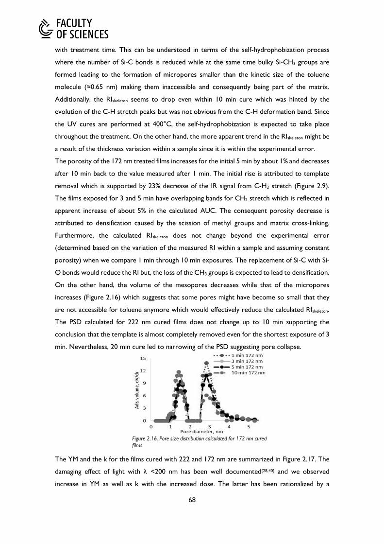
68
with treatment time. This can be understood in terms of the self-hydrophobization process
where the number of Si-C bonds is reduced while at the same time bulky Si-CH3 groups are
formed leading to the formation of micropores smaller than the kinetic size of the toluene
molecule (≈0.65 nm) making them inaccessible and consequently being part of the matrix.
Additionally, the RIskeleton seems to drop even within 10 min cure which was hinted by the
evolution of the C-H stretch peaks but was not obvious from the C-H deformation band. Since
the UV cures are performed at 400°C, the self-hydrophobization is expected to take place
throughout the treatment. On the other hand, the more apparent trend in the RIskeleton might be
a result of the thickness variation within a sample since it is within the experimental error.
The porosity of the 172 nm treated films increases for the initial 5 min by about 1% and decreases
after 10 min back to the value measured after 1 min. The initial rise is attributed to template
removal which is supported by 23% decrease of the IR signal from C-H2 stretch (Figure 2.9).
The films exposed for 3 and 5 min have overlapping bands for CH2 stretch which is reflected in
apparent increase of about 5% in the calculated AUC. The consequent porosity decrease is
attributed to densification caused by the scission of methyl groups and matrix cross-linking.
Furthermore, the calculated RIskeleton does not change beyond the experimental error
(determined based on the variation of the measured RI within a sample and assuming constant
porosity) when we compare 1 min through 10 min exposures. The replacement of Si-C with Si-
O bonds would reduce the RI but, the loss of the CH3 groups is expected to lead to densification.
On the other hand, the volume of the mesopores decreases while that of the micropores
increases (Figure 2.16) which suggests that some pores might have become so small that they
are not accessible for toluene anymore which would effectively reduce the calculated RIskeleton.
The PSD calculated for 222 nm cured films does not change up to 10 min supporting the
conclusion that the template is almost completely removed even for the shortest exposure of 3
min. Nevertheless, 20 min cure led to narrowing of the PSD suggesting pore collapse.
The YM and the k for the films cured with 222 and 172 nm are summarized in Figure 2.17. The
damaging effect of light with λ <200 nm has been well documented[28,40] and we observed
increase in YM as well as k with the increased dose. The latter has been rationalized by a
Figure 2.16. Pore size distribution calculated for 172 nm cured
films

69
densification caused by the removal of C-species and condensation of the formed radicals. It is
remarkable, however, that we observed k≈2.3 with improved YM of 7.6 GPa as compared to
5.7 GPa for the 2h thermally treated film. On the other hand, in order to avoid damaging the
low-k, light with λ >200 nm is usually preferred. As expected, the cure with λ =222 nm does
not have a detrimental effect on the k in the investigated range. Additionally, a beneficial effect
on the elastic modulus is observed – it increases steadily with treatment time from 5.5 GPa after
3 min up to 7.5 GPa after 20 min curing. We obtained similar k and YM for 1 min 172 nm and
20 min 222 nm treatment but the latter treatment is more suitable due to the lower remaining
template and the absence of silanol groups.
The inability of the light produced by the LP Hg sources to remove the template is reflected in
the calculated k for the films irradiated for 10 min – 2.36 and 2.34 for 254 and 185/254 nm
photons, respectively. These values are ≈0.1 lower than the film which was only thermally
treated for 10 min. This finding confirms the potency of the light to assist the template removal
if higher intensity source is employed.
The chemical stability of the films in 0.5wt% HF has been investigated. The films irradiated
between 3 and 10 min with 172 nm light are completely etched within less than one minute as
a result of the replaced SiCH3 with SiOH groups. The film cured for 1 min is etched for longer
than 3 min, indicating lower damage by the VUV photons. On the other hand, 4 min HF dip leads
to internal etching deduced by a decrease of the RI from 1.27 to 1.23 accompanied also by a
thickness loss of ≈25%. The films exposed to LP Hg lamps and the thermally treated reference
samples, are removed in about 6-7 min. The samples irradiated with 222 nm photons for up to
10 min show decreased chemical stability being completely etched in less than 4 min. Twenty
minutes cure, on the other hand, improved the chemical stability up to 5 min.
SE modelling was performed on films dipped in HF for a duration 1 min shorter than needed for
a complete dissolution. Using isotropic one-layer Cauchy function, the model becomes less
adequate as compared to the films before dipping in HF resulting in an increase of the associated
mean square error. The observed dispersion is better modelled by a two-layer Cauchy model.
For the top layer a thickness of ≈200 nm corresponding to a RI=1.27 is calculated, while a
Figure 2.17. Young's modulus and k value as a function of dose
(Intensity × treatment time)

70
thickness less than 5 nm associated to a RI≈1 is reported for the bottom layer. These findings
suggest that the Si-low-k interface play an important role in the explanation of the apparent
difference in the chemical stability. In order to investigate if there are changes in the interfacial
energy during HF dip, a tape-pull test was performed. The 2 h annealed film is easily removed
by the tape after 5 min HF dip, unlike the non-dipped film which remains on the Si substrate.
Quantification of the interface energies with and without 5 min dip in 0.5 wt% HF was performed
by nanoindention tests using wedge indenter. For the HF-treated sample a pop-in, early
indication for the formation of interface cracks, is observed (Figure 2.18) at a lower load than
for the pristine one. By using the semi-empirical solution introduced by Yeap et al.,[52] the
interfacial adhesion (Gc) for pristine and HF-dipped films are calculated to be 3.9 and 0.9 J/m2,
respectively. The Gc values are understood in the context of a preferential etching of the layer
close to the interface. Therefore, the faster HF etch of the film irradiated with 222 nm photons
compared to the reference thermally treated films seems to be due to difference in chemical
composition of the bottom layer. The difference might be related to remaining template in the
bottom of the thermally treated films which would be the most difficult to remove unlike the
UV-treated-films where the template removal is uniform.[40] However, a film annealed for 2 h
and consequently UV-treated with a broad band UV source (λ >200 nm), removing the
remaining template, did not result in a shorter chemical stability. This observation might be
explained by the more extended hydrophobization which would have occurred for 2h anneal.
The latter is supported by the observation that the HF stability improves by about 1 min after a
20 min as compared to a 10 min 222 nm UV-cure.
In order to elucidate the mechanism of the HF etch, ToF-SIMS analysis was performed on 222
nm cured and 2h annealed films before and after HF dip. There are no differences in the profiles
of Si-, C- and O-. Following the HF dip, the concentration of F- increases (Figure 2.19) throughout
the thickness of the film. Furthermore, we observe more significant F- accumulation close to the
Figure 2.18. Load-displacement curves from wedge indentation tests;
Inset: SPM images of (left) reference low-k after HF dip and (right)
reference (2 h thermal anneal) low-k film

71
Si interface. Additionally, three times higher increase of F- is detected after HF-dip for the film
cured with 222 nm photons compared to the HF-dipped reference film. The latter observation
correlates with the almost twice faster dissolution of the 222 nm irradiated films. Considering
the faster F- accumulation at the low-k-Si interface in light of the observed decrease of the
interfacial energy with HF dip we deduce the existence of a driving force for the interfacial F-
build-up. The driving force might be due to a hydrophilic layer containing OH- groups which
have been reported[53] to be eliminated and replaced by F- as a major reaction route for SiO2
dissolution in HF solution with pH>1.5.
2.3.3. UV cure of methylene-bridged oxycarbosilanes low-k films with a target k=2.0
Upon UV cure, the same trends in the electrical and mechanical properties are observed for the
more porous film of SBA Materials with a target dielectric constant of 2.0. Considering the
postulated by Rakhimova et al.[20] porosity dependence of the quantum efficiency of the photo-
induced C-depletion, we compare the effect of the 222 nm and 172 nm photons on the
concentration of the Si-CH3 bonds as deduced by the intensity of the absorption at 1275 cm-1
(Figure 2.20). Notably, the comparison is performed on FTIR spectra normalized to the intensity
of the peak corresponding to the Si-O-Si stretching at ≈1035 cm-1. The latter is a suitable
normalization when the films being compared have different densities. When the change of the
methyl concentration is compared between the two MeLK films, no evidence is observed for an
increased quantum efficiency in the removal of the methyl groups. The 2.0 and 2.2 versions of
the MeLK films maintain a similar methyl concentration as a function of the exposure time to
Figure 2.19. ToF-SIMS F- profiles of reference (2 h anneal) and 3 min
222 nm cured films before and after HF dip
Figure 2.20. Effect of the a) 172 nm and b) 222 nm UV cure on the Si-CH3 bond concentration deduced by FTIR spectra

72
the source with λ =172 nm (Figure 2.20 a). Additionally, the Si-CH3 concentration seems to be
similar in the MeLK2.2 and MeLK2.0 films given that the 222 nm photons were shown not to
affect the Si-CH3 groups (Figure 2.20 b). The only consistent difference between the FTIR spectra
of the two films is the stronger contribution from the cage structure in the MeLK2.0 films (not
shown) which is known to correlate with the low-k porosity.[37] Since generally the same
chemical modifications were observed for the MeLK2.2 and MeLK2.0 films, the discussion will
not be repeated here.
Similar to the MeLK2.2, both the 172 nm and the 222 nm cures lead to an increase of the Young’s
modulus of the MeLK2.0 with the increase in UV dose (Figure 2.21 a). Also, the improvement
of the mechanical properties is more significant for the higher energy photons. Nevertheless,
the damaging effect of the 172 nm light to the carbon content in the low-k results in
hydrophilization and lower stability against the moisture absorption and as a result the dielectric
constant increases in parallel with the YM. In contrast, the dielectric constant decreases with
increasing the UV dose of the 222 nm light. Interestingly, for the 222 nm UV cure, no saturation
is observed of both the YM increase and the k-value decrease and after a 20 min UV cure the
YM becomes 5.55 GPa and the k reaches 2.07. These properties are comparable to the
oxycarbosilane films reported by IBM[6,54] which is remarkable since the MeLK2.0 film is not
synthesized by a pure bridged precursor (e.g. BTESM or BTESE) and as a result, it is expected
to have a lower matrix connectivity as compared to IBM’s reports. Interestingly, the decrease in
dielectric constant upon UV cure with 222 nm is observed in spite of the decrease in porosity
(Figure 2.21 b). Since the calculated porosity reflects only the volume accessible to toluene, the
decreased porosity might be the result of the creation of micropores smaller than 0.6 nm, the
kinetic size of toluene, rather than an overall increase in film density. The micropores, on the
other hand, might be created as a result of the self-hydrophobization process. Importantly, since
the same trends are observed in the MeLK2.2 films, we conclude that the beneficial effect of the
222 nm UV cure reproducibly results in films with promising low-k properties. Furthermore, it
would be interesting to increase the UV dose further in order to find out when the beneficial
effects saturate or reverse.
Figure 2.21. a) Young's modulus and dielectric constant, and b) porosity as a function of UV dose. The lower dose
corresponds to the 172 nm UV cure while the higher dose - to the 222 nm UV cure

73
2.4. Conclusions
In conclusion, the UV and VUV irradiation has a more detrimental effect on ethylene-bridged
oxycarbosilane films as compared to those containing methylene groups. While it is known that
photons with energy lower than 6.2 eV (e.g. λ =222 nm) do not have any detrimental effect on
the Si-CH3 content, we showed that this also applies for the bridging methylene groups. On the
other hand, the concentration of the bridging ethylene groups is reduced even by the 222 nm
light. The difference in the stability of these two alkylene groups is more apparent when the films
are exposed to 172 nm light. The ethylene groups are depleted by more than 75% while
methylene loss is limited to only 40%. The experimental results were qualitatively supported by
DFT quantum chemical calculations.
We noted that the methylene groups (Si-CH2-Si) were affected little by the employed photon
energies between 4.9 and 7.2 eV. The UV doses achieved by the LP Hg sources were insufficient
to remove the template. Comparable k and Young’s modulus values (k≤2.3, YM ≥ 7.5 GPa) were
shown after 1 min 172 nm and 20 min 222 nm irradiations, but the latter produced superior
low-k films because of a better template removal and hydrophilization discernible from the FTIR
spectra. Based on the analysis of the EP data, we showed that the longer UV cure causes
densification of the film, while the matrix becomes less dense. The latter was rationalized in
terms of the expected reorganizations within the oxycarbosilane films, the self-hydrophobizaiton
reaction. The effects of the UV cure were reproduced on higher porosity films for which the
best low-k properties were obtained following a 20 min of 222 nm UV cure. In particular, a YM
of 5.5 GPa was calculated for a film with a dielectric constant of 2.07. Finally, we postulated a
role of the low-k-to-substrate interface in determining the stability of the films in an aqueous HF
solution.
2.5. References
[1] M. R. Baklanov, K. Maex, Philos. Trans. A. Math. Phys. Eng. Sci. 2006, 364, 201.
[2] W. Volksen, R. D. Miller, G. Dubois, Chem. Rev. 2010, 110, 56.
[3] E. T. Ryan, D. Priyadarshini, S. M. Gates, H. Shobha, J. Chen, K. Virwani, A. Madan, E.
Adams, E. Huang, E. Liniger, D. Collins, M. Stolfi, K. S. Yim, A. Demos, A. Grill, 2015 IEEE
Int. Interconnect Technol. Conf. 2015 IEEE Mater. Adv. Met. Conf. IITC/MAM 2015 2015,
349.
[4] A. Grill, S. M. Gates, T. E. Ryan, S. V. Nguyen, D. Priyadarshini, Appl. Phys. Rev. 2014, 1,
11306.
[5] E. Todd Ryan, S. M. Gates, S. A. Cohen, Y. Ostrovski, E. Adams, K. Virwani, A. Grill, J. Appl.
Phys. 2014, 115, 144107.

74
[6] G. Dubois, W. Volksen, T. Magbitang, R. D. Miller, D. M. Gage, R. H. Dauskardt, Adv.
Mater. 2007, 19, 3989.
[7] H. Li, J. M. Knaup, E. Kaxiras, J. J. Vlassak, Acta Mater. 2011, 59, 44.
[8] B. D. Hatton, K. Landskron, W. Whitnall, D. D. Perovic, G. A. Ozin, Adv. Funct. Mater. 2005,
15, 823.
[9] D. Jauffrès, R. Dendievel, M. Verdier, Thin Solid Films 2011, 520, 430.
[10] H. Fan, C. Hartshorn, T. Buchheit, D. Tallant, R. Assink, R. Simpson, D. J. Kissel, D. J. Lacks,
S. Torquato, C. J. Brinker, Nat. Mater. 2007, 6, 418.
[11] D. J. Michalak, J. M. Blackwell, J. M. Torres, A. Sengupta, L. E. Kreno, J. S. Clarke, D.
Pantuso, J. Mater. Res. 2015, 30, 3363.
[12] H. Kazi, R. James, S. Gaddam, U. Chiluwal, J. Rimsza, J. Du, J. Kelber, In Interconnect
Technology Conference / Advanced Metallization Conference (IITC/AMC); 2014; pp. 237–
240.
[13] S. Sugahara, K. I. Usami, M. Matsumura, Japanese J. Appl. Physics, Part 1 Regul. Pap. Short
Notes Rev. Pap. 1999, 38, 1428.
[14] B. Hatton, K. Landskron, W. Whitnall, D. Perovic, G. A. Ozin, Acc. Chem. Res. 2005, 38,
305.
[15] M. R. Baklanov, C. Adelmann, L. Zhao, S. De Gendt, ECS J. Solid State Sci. Technol. 2014,
4, Y1.
[16] P. Marsik, A. M. Urbanowicz, P. Verdonck, D. De Roest, H. Sprey, M. R. Baklanov, Thin
Solid Films 2011, 519, 3619.
[17] A. M. Urbanowicz, K. Vanstreels, P. Verdonck, D. Shamiryan, S. De Gendt, M. R. Baklanov,
J. Appl. Phys. 2010, 107, 104122.
[18] A. Zenasni, F. Ciaramella, V. Jousseaume, C. Le Cornec, G. Passemard, J. Electrochem. Soc.
2007, 154, G6.
[19] H. Shi, D. Shamiryan, J. F. de Marneffe, H. Huang, P. S. Ho, M. R. Baklanov, In Advanced
Interconnects for ULSI Technology; John Wiley & Sons, Ltd: Chichester, UK, 2012; pp. 79–
128.
[20] T. V. Rakhimova, A. T. Rakhimov, Y. A. Mankelevich, D. V. Lopaev, A. S. Kovalev, A. N.
Vasil’eva, S. M. Zyryanov, K. Kurchikov, O. V Proshina, D. G. Voloshin, N. N. Novikova, M.
B. Krishtab, M. R. Baklanov, J. Phys. D. Appl. Phys. 2014, 47, 25102.
[21] B. Jinnai, S. Fukuda, H. Ohtake, S. Samukawa, J. Appl. Phys. 2010, 107, 43302.
[22] N. Matsunaga, H. Okumura, B. Jinnai, S. Samukawa, Jpn. J. Appl. Phys. 2010, 49, 04DB06.
[23] S. Uchida, S. Takashima, M. Hori, M. Fukasawa, K. Ohshima, K. Nagahata, T. Tatsumi, J.

75
Appl. Phys. 2008, 103, 73303.
[24] W. Volksen, S. Purushothaman, M. Darnon, M. F. Lofaro, S. a. Cohen, J. P. Doyle, N. Fuller,
T. P. Magbitang, P. M. Rice, L. E. Krupp, H. Nakagawa, Y. Nobe, T. Kokubo, G. J. M. Dubois,
ECS J. Solid State Sci. Technol. 2012, 1, N85.
[25] M. Redzheb, L. Prager, M. Krishtab, S. Armini, K. Vanstreels, A. Franquet, P. Van Der
Voort, M. R. Baklanov, Microelectron. Eng. 2016, 156, 103.
[26] S. Eslava, F. Iacopi, A. M. Urbanowicz, C. E. a. Kirschhock, K. Maex, J. a. Martens, M. R.
Baklanov, J. Electrochem. Soc. 2008, 155, G231.
[27] a. M. Urbanowicz, B. Meshman, D. Schneider, M. R. Baklanov, Phys. Status Solidi 2008,
205, 829.
[28] E. a. Smirnov, K. Vanstreels, P. Verdonck, I. Ciofi, D. Shamiryan, M. R. Baklanov, M.
Phillips, Jpn. J. Appl. Phys. 2011, 50, 05EB03.
[29] S. M. Gates, D. a. Neumayer, M. H. Sherwood, A. Grill, X. Wang, M. Sankarapandian, J.
Appl. Phys. 2007, 101, 94103.
[30] J. Heo, H. J. Kim, J. Han, J.-W. Shon, Thin Solid Films 2007, 515, 5035.
[31] C. Rau, W. Kulisch, Thin Solid Films 1994, 249, 28.
[32] V. Rebbin, M. Jakubowski, S. Pötz, M. Fröba, Microporous Mesoporous Mater. 2004, 72,
99.
[33] F. Hoffmann, M. Güngerich, P. J. Klar, M. Fröba, J. Phys. Chem. C 2007, 111, 5648.
[34] T. Asefa, M. J. MacLachlan, H. Grondey, N. Coombs, G. A. Ozin, Angew. Chemie Int. Ed.
2000, 39, 1808.
[35] C. Vercaemst, J. T. a Jones, Y. Z. Khimyak, J. C. Martins, F. Verpoort, P. Van Der Voort,
Phys. Chem. Chem. Phys. 2008, 10, 5349.
[36] Y. Kayaba, F. Nishiyama, Y. Seino, T. Kikkawa, J. Phys. Chem. C 2011, 115, 12981.
[37] A. Grill, D. A. Neumayer, J. Appl. Phys. 2003, 94, 6697.
[38] S. Sugahara, T. Kadoya, K. Usami, T. Hattori, M. Matsumura, J. Electrochem. Soc. 2001,
148, F120.
[39] A. M. Dattelbaum, M. L. Amweg, J. D. Ruiz, L. E. Ecke, A. P. Shreve, A. N. Parikh, J. Phys.
Chem. B 2005, 109, 14551.
[40] L. Prager, P. Marsik, L. Wennrich, M. R. Baklanov, S. Naumov, L. Pistol, D. Schneider, J. W.
Gerlach, P. Verdonck, M. R. Buchmeiser, Microelectron. Eng. 2008, 85, 2094.
[41] V. Jousseaume, A. Zenasni, O. Gourhant, L. Favennec, M. R. Baklanov, Adv. Interconnects
ULSI Technol. 2012, 35.
[42] A. D. Becke, J. Chem. Phys. 1996, 104, 1040.

76
[43] C. Lee, W. Yang, R. G. Parr, Phys. Rev. B 1988, 37, 785.
[44] R. Bauernschmitt, R. Ahlrichs, Chem. Phys. Lett. 1996, 256, 454.
[45] P. Innocenzi, J. Non. Cryst. Solids 2003, 316, 309.
[46] M. Kanezashi, M. Kawano, T. Yoshioka, T. Tsuru, Ind. Eng. Chem. Res. 2012, 51, 944.
[47] R. Van Grieken, G. Calleja, G. D. Stucky, J. a. Melero, R. a. García, J. Iglesias, Langmuir
2003, 19, 3966.
[48] P. G. Pai, J. Vac. Sci. Technol. A Vacuum, Surfaces, Film. 1986, 4, 689.
[49] M. Milosevic, S. W. King, ECS J. Solid State Sci. Technol. 2015, 1, N3146.
[50] Y.-H. Kim, M. S. Hwang, H. J. Kim, J. Y. Kim, Y. Lee, J. Appl. Phys. 2001, 90, 3367.
[51] M. Baklanov, K. Maex, M. Green, Dielectric Films for Advanced Microelectronics;
Baklanov, M. R.; Green, M. L.; Maex, K., Eds.; John Wiley & Sons, Ltd: Chichester, UK,
2007.
[52] K. B. Yeap, K. Zeng, H. Jiang, L. Shen, D. Chi, J. Appl. Phys. 2007, 101, 123531.
[53] Q. T. Le, G. Vereecke, H. Struyf, E. Kesters, M. R. Baklanov, In Advanced Interconnects for
ULSI Technology; John Wiley & Sons, Ltd: Chichester, UK, 2012; pp. 129–171.
[54] G. Dubois, W. Volksen, T. Magbitang, M. H. Sherwood, R. D. Miller, D. M. Gage, R. H.
Dauskardt, J. Sol-Gel Sci. Technol. 2008, 48, 187.

77
CHAPTER 3. EFFECT OF LASER ANNEAL ON
OXYCARBOSILANE LOW-K PROPERTIES
This chapter describes the investigation of the laser anneal’s ability to remove the template from
and to improve the Young’s modulus of oxycarbosilane low-k films. The work was performed
in a collaboration with Ultratech who performed the laser anneals in their facility in San Jose,
California, USA. As a result, this work was performed in two stages. The first stage included
laser anneal of as-deposited films in ambient lab atmosphere by two different laser sources – a
visible wavelength nanosecond laser with λ =532 nm and an infrared CO2 laser with λ =10.6
μ m. Nevertheless, only the results from the anneal with the IR laser are included here since no
template removal was observed following the anneal with the visible laser. In the second stage,
the laser anneals were performed in a controlled N2 atmosphere with the same IR laser source.
The IR laser anneal affects mostly the organic content of the organosilicate matrix leading to
depletion and reorganization. Nevertheless, when compared to a reference film annealed in a
furnace at 400°C for 2 h, the tested conditions reveal a processing window which allows for a
13% improvement of the Young’s modulus while not impacting the dielectric constant of 2.25.
M. Redzheb, S. Armini, K. Vanstreels, J. Meersschaut, M. R. Baklanov, Y. Wang, S. Chen, V. Le, M.
Awdshiew, P. Van Der Voort, Laser anneal of oxycarbosilane low-k film, 2016 IEEE International
Interconnect Technology Conference / Advanced Metallization Conference (IITC/AMC), 156-158 (2016)

78
3.1. Introduction
Reliable ultra-low-k materials are needed in order to reduce the resistance-capacitance signal
delay in future generation ultra-large scale integrated interconnects.[1,2] In order to reduce the
dielectric constant below 2.5, porosity needs to be introduced in the organosilicate films.
However, due to the detrimental effect of this approach on the mechanical reliability, treatments
for improvement of the mechanical stability are under investigation. The most popular approach
for the enhancement of the Young’s modulus has been the application of ultra-violet (UV)
irradiation with a wavelength longer than 200 nm. The UV cure (UV irradiation at temperature
≈ 400°C) is used for both template removal and to promote crosslinking in the porous film.
Alternatively, a short pulse laser anneal has been investigated for improving the mechanical
properties of low-k films. Volksen and co-authors[3] investigated the laser anneal of dense and
porous organosilicate films and noted the ability of this approach to improve the Young’s
modulus with a limited negative impact on the dielectric constant. On the other hand, Raymunt
et al.[4] reported theoretical and experimental investigation of the effect of a laser anneal on the
bonding structure of an organosilicate low-k film. Nevertheless, these studies did not consider
the laser anneal for a porogen removal or investigate its effects on oxycarbosilane films which
contain backbone carbon as bridging alkylene (Si-(CH2)x-Si) groups. The latter have been
shown[5,6] to be more promising low-k candidates than the conventional carbon-doped oxides
where carbon is present solely as –CH3 groups.
3.2. Experimental Section
The investigated films were prepared by using the sol-gel method where a stabilized sol is spin-
deposited onto a Si substrate. The coating sol was prepared by mixing a matrix and a template
solution. The former was obtained by stirring 1.1 ml 1,2-bis(triethoxysilyl)ethane (BTESE), 0.56
ml 0.02 molar hydrochloric acid, and 0.64 ml methyltriethoxysilane (MTES) in 2 ml ethanol at
60°C for 1 hour. The BTESE is the source of the bridging ethylene groups (Si-CH2-CH2-Si) while
the MTES is the source of methyl groups making the film hydrophobic. In parallel, the template
solution was prepared by dissolving 0.3763 g polyoxyethylene (18) tridecyl ether in 16 ml 1-
methoxy-2-propanol after stirring for ca. 45 min at room temperature (RT). Next, the template
solution was added to the cooled down to RT matrix solution and further stirred for 15 min at
RT. Finally, the mixture was transferred to a 50 ml polyethylene bottle and aged for 24 hours at
RT. In the first experiment, the solution was spin-coated on 3.5x3.5 cm square Si coupons while
in the second, on a 300 millimetre diameter Si wafer at 1500 rpm for 60 s. Following the
deposition, the film was soft baked at 150°C for 2 min in an ambient atmosphere in order to
promote polycondensation and solvent evaporation. The resulting thickness was ca. 216 nm. A
control sample was annealed in N2 atmosphere at 400°C for 2h.

79
The laser anneals from the first experiment were performed on a lab tool in a non-controlled
ambient atmosphere. Two laser sources were investigated – a green laser with λ =532 nm and
an infrared CO2 laser with an output peak around 943 cm-1 out of the resonance frequency of
the organosilicate matrix. The absorption of the CO2 radiation is facilitated by the free carriers
in the n-type Si substrate.[4] Temperatures between 725 and 1180°C were detected by a
pyrometer calibrated to the melting temperature of an undoped Si. Two laser exposure
durations (dwell time), 400 and 800 μs, were investigated. The samples were additionally heated
by a hot plate at 150°C.
At stage two, the soft-baked wafer was laser-annealed in an Ultratech LSA201 system equipped
with a CO2 infrared laser. Eight power densities with a dwell time of 800 μ s were used to
generate eight test patterns with width of 30 mm on the wafer. The scanning step size was 25%
meaning that each spot was annealed four times. These annealing conditions allow for a wafer
300 mm in diameter to be annealed within 3 min. The wafer was additionally heated by a hot
plate at 150°C. Temperatures between 900 and 1145°C were detected by the pyrometer. The
treatments were performed in an inert N2 atmosphere.
3.3. Results and Discussion
3.3.1. Screening for laser anneal conditions for oxycarbosilanes low-k films
The temperature values observed during the laser anneal (LA) cannot be directly compared to
the furnace anneal temperature. One reason is the fact that the temperature deduced during LA
is that of the silicon substrate and the thermal profile normal to the substrate is not available. In
other words, it is not entirely clear the actual temperature to which the low-k is exposed.
Furthermore, unlike a furnace anneal where the low-k films are exposed to the set temperature
for hours, the LA is less than a millisecond. For instance, it has been demonstrated that resist
films can be annealed at a ~3 times higher temperature than their glass transition temperature
when employing sub-millisecond laser anneal.[7]
Increasing the laser power, which corresponds to an increase in substrate temperature, results
in a decrease of the refractive index indicating the removal of the template (Figure 3.1). The
Figure 3.1. Refractive index (a) and Δ thickness (b) as a function of laser anneal temperature compared to a reference
annealed at 400°C for 2h in N2

80
lowest RI is reached for the highest temperature of 1142°C which is close to the melting
temperature of the silicon substrate. Still, the lowest RI of 1.3 achieved by the laser anneal is
higher than the RI of the reference film, 1.26 (Figure 3.1). The latter is probably due to a
densification or a pore collapse of the low-k matrix caused by the high annealing temperatures.
This explanation is supported by the higher than the 12% reference thickness change observed
for the films annealed at a temperature higher than 1000°C (Figure 3.1). Furthermore, the
porosity of the film laser annealed at 1142°C is 32.8% as compared to the 38% porosity of the
reference film.
Based on the FTIR spectra, the template seems not completely removed at temperatures around
and below 1000°C. The presence of the template can be deduced by considering both the strong
C-H2 stretch-related absorptions at 2885 cm-1 and 2910 cm-1 and the broad –OH-related
absorption between 3100 cm-1 and 3700 cm-1. The evolution of the template removal can also
be monitored from a peak at 1730 cm-1 which is not present in the as-deposited films and appears
following the laser anneal. The peak is attributed to the formation of C=O bonds as part of a
formic acid termination identified during the thermal decomposition of poly(ethylene oxide)-
containing molecules in an ambient oxygen-containing atmosphere.[8]
Remarkably, according to the FTIR analysis, the laser anneal does not seem to affect the carbon
covalently bonded to the matrix, i.e. the ethylene and the methyl groups, below a temperature
of 1000°C. The intensity of the peaks attributed to the methyl and ethylene absorptions at 1275
cm-1 and 1412 cm-1, respectively, does not change below a temperature of 1000°C (Figure 3.2).
Nevertheless, the temperature required for a complete template removal, as inferred from the
lowest value of RI, which is higher than 1000°C cause a significant carbon depletion from the
low-k matrix. Unfortunately, FTIR does not allow for a definite analysis of which among the
a)
Figure 3.2. FTIR spectra showing a) the template removal efficiency of the laser anneal and b) its
effect on the low-k matrix
a)
b)

81
methyl and the ethylene groups are more strongly affected by the laser anneal since the two
peaks mentioned, 1275 cm-1 and 1412 cm-1, have been attributed to both the Si-CH3[9] and Si-
CH2-CH2-Si[10] groups since they are the result of the deformational modes of the C-H bonds.
On the other hand, the C-Hx stretching modes at wavenumbers just below 3000 cm-1 overlap
with absorptions from the template for which it is difficult to deduce whether it is completely
removed. It seems more likely that effectively the ethylene groups would be depleted
preferentially since they might be transformed into methyl groups by a scission of the C-C bonds.
More importantly, an evidence of the preferential ethylene groups’ depletion can be obtained
from a more detailed analysis of the 1275 cm-1 peak. When the peak is observed in a low-k film
containing carbon only as Si-CH3 groups, it is narrower than when there is an additional
contribution from the ethylene groups. Compared to the laser anneal at 1000°C, the anneal at
1150°C results in a lower intensity but also a narrower peak at 1275 cm-1 showing the significant
depletion of the ethylene groups whose concentration seems to be so low that they do not
contribute to the 1275 cm-1 peak. Finally, the damaging effect of the 1150°C laser anneal is
manifested by the appearance of an absorption at 883 cm-1 which is attributed to the presence
of Si-H bonds which are most likely the result of the formation of dangling bonds which are
consequently passivated by H radicals formed from the decomposition of the organics.
3.3.2. IR laser anneal in a controlled inert atmosphere
Given the results from the first evaluation stage of the effect of the laser anneal on the low-k
films, in the second stage we focused on the laser anneal temperatures around 1000°C, in
particular between 900°C and 1145°C. Within this temperature range, the lowest RI is observed
at ≈1040°C while at lower and higher temperatures slightly higher RIs are measured (Figure 3.3)
but these differences in the temperature range above 980°C are not statistically significant.
Additionally, toluene ellipsometric porosimetry (EP) measurements reveal that there is no
difference in the open porosity, calculated to be 38 %, for the annealing conditions above 940°C.
The only condition which can definitely be claimed to result in an incomplete template removal
is the annealing at 900°C in which case 3% lower open porosity is calculated. The calculated
pore size distribution (PSD) further supports this interpretation by indicating narrower PSD for
Figure 3.3. Refractive index and open porosity results show that the laser anneal between 940°C and 1140°C leads to films
with similar optical properties

82
the film cured at 900°C which is explained by the remaining template on the pore walls effectively
making the pores smaller. No differences in the PSD are observed for the films annealed at a
temperature higher than 900°C. The EP data additionally indicates a lack of pore collapse or
significant densification which might have been expected[4] given the high temperatures achieved.
Furthermore, it is important to limit the shrinkage of the film since it contributes to the
compressive stress during integration. The shrinkage observed for the reference films, furnace
annealed at 400°C in N2 ambient for 2 h, is ca. 11 % while for the laser annealed films we observe
that increasing the laser power results in a steady increase of the shrinkage up to 19.4 % for the
highest laser power utilized in this study. The anneals at a temperature up to 1040°C allow to
achieve shrinkage comparable to the one observed in the reference film.
Nevertheless, the FTIR spectra (Figure 3.4) reveal removal of the organics from the film even
for the lowest laser power applied. This is further observed in the ERD spectra where C content
decreases from ca. 22% to 15% when the anneal temperature exceeds 1000°C. Furthermore,
FTIR analysis indicates faster reduction of the bridging ethylene groups as compared to the
methyl groups and virtually complete depletion at the highest laser power. ERD and FTIR further
agree on the Si-O bond formation which is seen in the FTIR spectra as a blue shift as well as
intensity increase of the region attributed mainly to Si-O-Si absorption and as an increase in the
relative content of Si and O in the ERD spectra. Nevertheless, while based on the FTIR spectra,
a further removal of organics with higher temperature is apparent, the C-content deduced from
the ERD spectra stays constant. The latter might point to a bond redistribution which was
Figure 3.4. FTIR spectra of the laser annealed films compared to the reference film annealed at 400°C for 2h

83
discussed in a previous study.[3] One manifestation of the bond rearrangements seems to be the
formation of Si-CH2-Si groups evident by a weak peak at 1360 cm-1. The latter can be explained
by the cleavage of the C-C bonds in ≡ Si-CH2-CH2-Si≡ groups in combination with the presence
of ≡ Si• radical due to ≡ Si-CH3 bond dissociation. Another modification of the films evident by
peaks at 885 and 2245 cm-1 is the appearance of ≡ Si-H bonds. These compositional changes
evident from the FTIR spectra reveal the numerous passivation processes occurring with the
≡ Si• radicals formed due to the breaking of the ≡ Si-C bonds. Additionally, the C-extraction
leads to surface hydrophilization for the highest temperatures achieved. The surface water
contact angle (WCA) was measured to be around 90° for temperatures below 1100°C while at
a T≥1100°C, a statistically significant decrease of the WCA occurs leading to a value of 80° after
applying the highest laser power.
The modifications of the films were further monitored by spectroscopic ellipsometry in the
range from 1.4 to 8 eV. The ellipsometric dispersion observed for the samples annealed at a
temperature higher than 1000°C can be modelled by the sum of two Lorentz oscillators while
only one is sufficient for the film annealed at 900°C. The absorption common for all of the
samples is centered at ca. 8.5 eV and is attributed to the optical bandgap of the low-k.[11,12] On
the other hand, the second absorption is centered at 6.7 eV (Figure 3.5). The latter may be
attributed to the formation of O3≡ SiSiSi≡ O3 structures[13] which once again indicate the
extensive modifications of the low-k matrix.
The Young’s modulus and the dielectric constant values increase with higher laser power (Figure
3.6) which is consistent with the deduced bond rearrangements. The higher k observed for the
film cured at 900°C also supports the hypothesis for an incomplete template removal. In spite
of the relatively damaging effect of the laser anneal to the chemical structure of the low-k film,
we find a window of processing conditions around 1000°C which results in virtually the same
dielectric constant as for the reference film and a higher elastic modulus. In particular, the laser
anneal at 1015°C leads to about a 13% higher YM value of 4.59 GPa as compared to the
Figure 3.5. Modelled spectroscopic ellipsometric dispersion of the extinction coefficient showing the appearance of an
absorption at 6.7 eV when the film is annealed at a temperature higher than 1000°C

84
reference film with YM=4.07 GPa and the dielectric constant calculated for both of the films is
2.25.
3.4. Conclusions
Laser anneal was investigated for porogen removal and its ability to improve the mechanical
strength of oxycarbosilane ultra low-k films. The increase in the Young’s modulus is the result
of the high activation energy achieved as a result of the high temperatures around and in excess
of 1000°C which ensures the condensation of the silanol groups and the densification of the
matrix. High laser power corresponding to a surface temperature of ca. 1000°C is required in
order to achieve complete template removal. To obtain a -OH-free low-k film, the laser anneal
needs to be performed in an inert atmosphere. Extensive bond rearrangements mostly related
to the replacement or reorganization of the organic content of the organosilicate matrix are
shown. Around 1000°C, there exists a processing window which allows for a 13% higher Young’s
modulus value as compared to the reference films annealed in a furnace at 400°C, with no impact
on the dielectric constant calculated to be 2.25. Remarkably, no significant film densification is
deduced within the processing window.
3.5. References
[1] M. R. Baklanov, C. Adelmann, L. Zhao, S. De Gendt, ECS J. Solid State Sci. Technol. 2014,
4, Y1.
[2] G. Dubois, W. Volksen, In Advanced Interconnects for ULSI Technology; John Wiley &
Sons, Ltd: Chichester, UK, 2012; pp. 1–33.
[3] W. Volksen, G. Dubois, A. Kellock, T. P. Magbitang, R. D. Miller, D. Miller, S. Cohen, E. E.
Simonyi, L. Ramirez, D. Markle, S. Chen, S. Zhou, X. Wang, Y. Wang, J. Electrochem. Soc.
2008, 155, G224.
[4] A. M. Raymunt, R. T. Bell, M. O. Thompson, P. Clancy, J. Phys. Chem. C 2015, 119, 12616.
[5] G. Dubois, W. Volksen, T. Magbitang, R. D. Miller, D. M. Gage, R. H. Dauskardt, Adv.
Mater. 2007, 19, 3989.
[6] D. J. Michalak, J. M. Blackwell, J. M. Torres, A. Sengupta, L. E. Kreno, J. S. Clarke, D.
Figure 3.6. Dielectric constant and Young's modulus as a function of the laser annealing temperature

85
Pantuso, J. Mater. Res. 2015, 30, 3363.
[7] F. Bérubé, S. Kaliaguine, Microporous Mesoporous Mater. 2008, 115, 469.
[8] A. Grill, D. A. Neumayer, J. Appl. Phys. 2003, 94, 6697.
[9] S. Sugahara, K. I. Usami, M. Matsumura, Japanese J. Appl. Physics, Part 1 Regul. Pap. Short
Notes Rev. Pap. 1999, 38, 1428.
[10] S. W. King, B. French, E. Mays, J. Appl. Phys. 2013, 113, 44109.
[11] X. Guo, H. Zheng, S. W. King, V. V. Afanas’ev, M. R. Baklanov, J.-F. de Marneffe, Y. Nishi,
J. L. Shohet, Appl. Phys. Lett. 2015, 107, 82903.
[12] K. Awazu, H. Kawazoe, K. I. Muta, J. Appl. Phys. 1991, 70, 69.

86

87
CHAPTER 4. PROPERTIES OF SELF-ASSEMBLY-BASED LOW-K
FILMS: EFFECT OF THE REPLACEMENT OF SI-O-SI BY SI-CH2-
SI
This chapter reports the effect of the replacement of Si-O-Si by Si-CH2-Si groups on the
mechanical and electrical properties of silica-based hybrid sol-gel thin films. For a reliable
inference, two sets of organosilica films were synthesized – one consisting of a silica matrix
decorated with methyl groups (Si-CH3) while the other further incorporating bridging methylene
(Si-CH2-Si) functionalities. As a result, at the film density of 0.87 g cm-3, a higher Young’s modulus
of 6.6 GPa was deduced for the film containing Si-CH2-Si groups compared to 5.3 GPa for the
one with Si-O-Si functionalities. Concurrently, the introduction of the methylene bridging groups
leads to a dielectric constant increase from 2.12 to 2.27. Furthermore, the type of surfactant,
ionic or nonionic, employed as a templating agent has a negligible effect on the electrical
properties and the reliability performance of the porous organosilica films. When dipped in 0.5
wt% HF, internal etching is observed for the films containing the methylene groups while the
films without the organic bridges are internally etched only if an organic solvent is added to the
aqueous HF solution.
M. Redzheb, S. Armini, T. Berger, M. Jacobs, M. Krishtab, K. Vanstreels, S. Bernstorff and P. Van Der
Voort, On the mechanical and electrical properties of self-assembly-based organosilicate porous films,
Journal of Materials Chemistry C, (2017)

88
4.1. Introduction
Silica-based porous materials are utilized as an antireflective, antifogging and superhydrophobic
coating on solar cells[1,2], interlayer and intermetal dielectrics in integrated circuits,
chromatographic supports, selective adsorbents[3], bone grafts for bone tissue regeneration[4],
sensors for environmentally responsive materials, photonic devices and others[5]. For many of
these applications, the mechanical stability of the porous silica-based material has a limiting role
on the overall device performance. As a result, the superior Young’s modulus (YM) values
reported for porous oxycarbosilane (OCS) and periodic mesoporous organosilica (PMOs) films
as compared to other silica-based films have attracted the attention of the semiconductor
industry[6–8]. The higher YM values have been attributed to the presence of the Si-(CH2)n-Si
units[6,9] which has been generally supported by the modelling work[10]. Nevertheless, deducing
the contribution of the organic bridging groups to the YM seems to be a difficult experimental
task when the films being compared are obtained via two different deposition techniques, e.g.
spin-on vs plasma-enhanced chemical vapour deposition (PECVD), or when the films are
expected to have a different matrix connectivity, like in methylsilsesquioxanes (MSSQ) vs
OCS.[11,12] Moreover, the matrix elastic moduli of OCS films reported[6,11–13] so far are lower
than those observed for silica. Additionally, the mechanical properties of polycarbosilane
films[14,15] have been shown to be similar to those of oxycarbosilanes. On the other hand, a direct
comparison between the YM of porous silica and porous OCS or PMO films is challenging due
to an overestimation of the YM in hydrophilic SiO2 films caused by the presence of absorbed
moisture.[16,17] Therefore, an appropriate comparison of the mechanical properties requires films
which are hydrophobic, possess similar pore volume and/or dielectric constant, as well as matrix
connectivity, and differ only in the presence of the organic bridging groups. In order to meet
these requirements, we synthesized two sets of films - one with a molar ratio of
tetraethylorthosilicate (TEOS) : methyltriethoxysilane (MTES) = 1:1 and the second with a molar
ratio of bis(triethoxysilyl)methane (BTESM) : methyltriethoxysilane (MTES) = 1:1. The TEOS and
BTESM precursors are the source of the Si-O-Si and Si-CH2-Si groups. The MTES precursor is
employed in order to obtain hydrophobic films[18–21]. Furthermore, the incorporation of the
precursors in the final films is expected to be similar between the two sets since the bridged
precursor bis(triethoxysilyl)ethane has been shown to have polycondensation kinetics similar to
TEOS.[20] As a result of the comparable precursor incorporation, a similar degree of matrix
connectivity is expected to be achieved. Finally, the pore volume can be controlled by optimizing
the surfactant to precursor ratio.
The use of surfactants in the synthesis solution enables the control of the films’ pore
arrangement (mesophase).[22] The films’ mesophase depends on the synthesis parameters such
as the surfactant to precursor ratio, the pH, the solution aging conditions such as the aging

89
temperature and time as well as the organosilica precursor.[5] All of these parameters, ultimately,
determine the degree of polycondensation and the size distribution of the organosilica
oligomers. Consequently, the interaction of the organosilica oligomers with the surfactant
molecules is one of the main determinants of the film’s final mesophase. On the other hand, the
mesophase can also be controlled by the deposition conditions such as the presence of an
electric field, the surface energy of the substrate, the vapour pressure of the solvents, the
ambient relative humidity, the atmospheric ethanol content, the deposition temperature and the
substrate’s spin speed.[5,23] Therefore, obtaining a desired mesophase using different surfactants
would require a specific and, probably, different organosilica oligomer distribution as well as
different surfactant to precursor ratios for each surfactant. Such an experimental design, in an
attempt to deduce the effect of the replacement of the Si-O-Si by the Si-CH2-Si groups, would
introduce the confounding variable of the significant differences in the films’ matrices and would,
most likely, result in large differences in the films’ pore volumes. Furthermore, if the pore order
is achieved in some of the films but not in the others or if the pore order is different in the
different films, the interpretation of the results would be further complicated. Instead, in this
study, the (organo)silica precursors are pre-condensed at 60°C for 1 h before the template is
introduced and the resulting solution is further aged at room temperature for 24 h before
deposition. These synthesis conditions combined with the use of 50% MTES make it unlikely that
an ordered porosity film will be achieved. The MTES disrupts the ordered porosity when it is
polycondensed together with the TEOS and the (organo)silica precursor mixture contains more
than 33% MTES.[24–26] The higher than 33% MTES content can be incorporated without disrupting
the mesophase by a two-step synthesis procedure where the MTES is introduced into the
solution just before the deposition.[27–29]
There are numerous studies which considered spin-coated organosilica dielectrics for low-k
application but none of them provides a systematic study of all the parameters on which the YM
depends. Ideally, in order to engineer the optimal YM for a low-k film one needs to consider
pore volume, film and skeleton densities, chemical composition, relative content of the different
siloxane ring sizes, average connectivity number of the skeleton, pore shape and organization,
as well as, pore size distribution. We compare the YM of the films as a function of Si-CH2-Si vs.
Si-O-Si functionalities incorporated into the matrix, while keeping constant the matrix
connectivity of the layers. In addition, the impact of the nature of the templating surfactant on
the electrical reliability of the low-k film is discussed.
4.2. Experimental Section
Tetraethylorthosilicate (TEOS), methyltriethoxysilane (MTES), 1-methoxy-2-propanol,
polyoxyethylene (10) stearyl ether (Brij-76), Polyoxyethylene (4) lauryl ether (BrijL4), Pluronic
F127 and cetyltrimethylammonium chloride (25 wt%, CTAC) were purchased from Sigma

90
Aldrich, bis(triethoxysilyl)methane (BTESM) was obtained from Fluorochem, hydrochloric acid
(HCl, 37%) was acquired from KMG Chemicals, and absolute ethanol (99.9%) was purchased
from Merck. All materials were used as received.
TEOS MTES BTESM surfactant Label1 1 1 0 0.126 MSQC 1 1 0 0.210 MSQL4 1 1 0 0.077 MSQS10 1 1 0 0.004 MSQF127 0 1 1 0.240 OCSC 0 1 1 0.320 OCSL4 0 1 1 0.124 OCSS10 0 1 1 0.004 OCSF127
Two types of organosilica thin films were prepared using a sol-gel method: one with silica matrix
and containing Si-CH3 groups (MSQ), and another with hybrid matrix containing both Si-CH2-Si
and Si-O-Si bonds as well as Si-CH3 groups (OCS). Furthermore, each matrix type was templated
by four different surfactants – one ionic, CTAC, and three non-ionic, Brij L4, Brij S10 and
Pluronic F127. The synthesis conditions were optimized in order to obtain films with similar
pore volume and details about the reagents’ molar ratios can be found in Table 4.1. A typical
synthesis included the preparation of two solutions, a matrix and a template solution, in parallel.
The matrix solution was obtained by mixing 2 ml ethanol, 0.58 ml 0.02 molar HCl, 1.048 ml
BTESM and 0.6 ml MTES by stirring and refluxing for 1 h at 60°C. When a film morphology is
desired, the acidic (organo)silica synthesis is more suitable than the neutral or basic pH since it
results in more polymer-chain-like (organo)silica oligomers.[30] In the meantime, the template
solution was prepared by mixing 0.34 ml BrijL4 with 12 ml 1-methoxy-2-propanol. Next, the
two solutions were mixed at room temperature and stirred for 15 min. Before deposition the
solutions were aged in a PE bottle at room temperature for 24 h. The solutions were spin-
coated at 1500 rpm on 300 mm Si wafers on which native oxide had been grown. Next, the films
were soft-baked at 150˚C in ambient atmosphere for 2 min and hard-baked at 400˚C in N2 for
2 h. Finally, in order to simulate a common practice in the IC industry, the films were UV-cured
at 400˚C in N2 for 2 min with a broadband UV source with λ >200 nm.[6]
Table 4.1. Molar ratio of the reagents employed in the synthesis of the films. 1The labels reflect the matrix composition,
MSQ for methylsilsesquioxane-like films and OCS for oxycarbosilane-like films, and the associated templating surfactant
where C=CTAC, L4=BrijL4, S10=BrijS10 and F127=PluronicF127
Figure 4.1. Structure of the employed (organo)silica precursors: a) TEOS; b) MTES; c) BTESM
a) b) c)

91
4.3. Results and Discussion
4.3.1. Chemical composition of OCS and MSQ films
As a result of the employed synthesis strategy, if the precursors contributed to the final matrix
compositions in proportions dictated by their molar ratios in the synthesis solutions, two times
larger carbon content would be expected in the OCS as compared to the MSQ films.
Consistently, a depth-resolved x-ray photoemission spectroscopy (XPS) study revealed that the
elemental composition of MSQ was Si:C:O = 35:8:57 as compared to 34:15:51 in OCS films
(Figure 4.2). Clearly, all of the carbon in the MSQ matrices is incorporated as methyl (-CH3)
groups. Nevertheless, the attribution of the additional carbon in the OCS films to methylene (-
CH2-) groups is not straightforward due to the self-hydrophobization[31] process which leads to
transformation of the methylene groups to methyl groups at elevated temperatures in the
presence of Si-OH. The higher carbon content in the OCS films is at the expense of the Si-O-Si
groups which is why the binding energy of the Si (2p) peak is lower in the OCS than in the MSQ
(Figure 4.2). Nevertheless, the binding energy of the Si 2p peak cannot provide a definitive proof
of the incorporation of the carbon in the OCS as a bridging Si-CH2-Si since in both (R3SiO)3-Si-
CH3 and (RO)3-Si-CH2-Si-(RO3), the silicon atom is in a T group, i.e. connected to three -O-SiR3
functionalities and one heterofunctionality such as the methyl and methylene groups. On the
other hand, in the OCS films, the chemical bonding environment of the carbon is expected to
consist of not only one silicon and three hydrogen atoms but also of two silicon atoms and two
hydrogen atoms. Therefore, the binding energy of the C (1s) peak in the OCS films indicates the
presence of the Si-CH2-Si groups.[32]
The chemical compositions of the films were further deduced from the FTIR spectra which were
normalized to the thickness of the films (Figure 4.3). In MSQ-like films, the band from 1000 to
1250 cm-1 is often peak-fitted with three peaks, linear (≈1037 cm-1), network (≈1071 cm-1) and
cage (≈1134cm-1) (Figure 4.4), which reflect, among other things, the distribution of the siloxane
Figure 4.2. Carbon 1s and silicon 2p XPS spectra of the OCS and MSQ films. The shown results were obtained
after half of the thickness of the films was etched away by Ar+ ions.
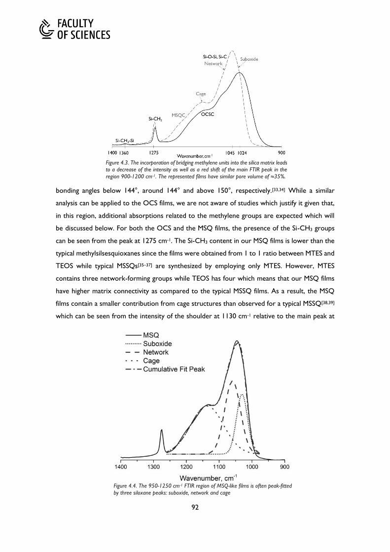
92
bonding angles below 144°, around 144° and above 150°, respectively.[33,34] While a similar
analysis can be applied to the OCS films, we are not aware of studies which justify it given that,
in this region, additional absorptions related to the methylene groups are expected which will
be discussed below. For both the OCS and the MSQ films, the presence of the Si-CH3 groups
can be seen from the peak at 1275 cm-1. The Si-CH3 content in our MSQ films is lower than the
typical methylsilsesquioxanes since the films were obtained from 1 to 1 ratio between MTES and
TEOS while typical MSSQs[35–37] are synthesized by employing only MTES. However, MTES
contains three network-forming groups while TEOS has four which means that our MSQ films
have higher matrix connectivity as compared to the typical MSSQ films. As a result, the MSQ
films contain a smaller contribution from cage structures than observed for a typical MSSQ[38,39]
which can be seen from the intensity of the shoulder at 1130 cm-1 relative to the main peak at
Figure 4.3. The incorporation of bridging methylene units into the silica matrix leads
to a decrease of the intensity as well as a red shift of the main FTIR peak in the
region 900-1200 cm-1. The represented films have similar pore volume of ≈35%.
Figure 4.4. The 950-1250 cm-1 FTIR region of MSQ-like films is often peak-fitted
by three siloxane peaks: suboxide, network and cage

93
1045 cm-1. Additionally, the template removal temperature of 400°C further decreases the
relative content of the siloxane cages due to their low thermal stability.[37,38] On the other hand,
the higher carbon content in OCS as compared to MSQ films is confirmed from the red shift of
the main peak, from 1045 to 1024 cm-1. Furthermore, the significant number of methylene
groups in the OCS films is proved by the presence of the peak at 1360 cm-1 as well as the
shoulder at 1080-1040 cm-1.[40,41] Additionally, the carbon incorporated in the network of the
matrix, as opposed to being in -CH3 groups, results in decreased intensity of the main Si-O-Si
peak further supporting the interpretation for the significant incorporation of methylene bridging
functionalities.
The different pore sizes and pore size distributions (Figure 4.5), resulting from the different
templating molecules, do not affect the low-k matrix bonding configuration as deduced from the
950-1400 cm-1 region of the FTIR spectra which are normalized to the intensity of the main peak
(Figure 4.6). In spite of the different pore structures, the spectra of the MSQ films with similar
pore volume (within 2 percentage points) overlap almost perfectly. Only the spectrum of the
MSQL4 film displays lower intensity of the high wavenumber shoulder around 1150 cm-1,
attributed to the cage siloxane structure[34], together with a red shift, from 1047 to 1042 cm-1,
of the main siloxane peak indicating an average Si-O-Si angle lower than 144°. Both observations
can be explained with the lower pore volume[34,42–46] calculated for the MSQL4 as compared to
the other MSQ films, 30 vs ≥37%. We observed a similar correlation for the OCS films (Figure
4.6) where larger pore volume differences than those for the MSQ films were calculated (Table
4.2). Nevertheless, the OCSL4 film seems to be an outlier since it has an open pore volume of
38%, similar to that of OCSC, but the high-wavenumber shoulder at ≈1140 cm-1 is as low as that
of OCSF127 which has open pore volume of 32.5%. Additionally, the main siloxane peak of the
OCSL4 film is red-shifted even in comparison to the lowest pore volume OCSF127 film, 1026
Figure 4.5. Pore size distributions (PSD) calculated from the adsorption branch of the
toluene EP isotherms for MSQ films. Similar PSDs were obtained for the OCS films

94
vs 1020 cm-1. The latter might be due to the fact that films with uniform nanoscale confinement
of the silica framework, deduced from the presence of a Debye-Scherrer ring in the GISAXS
pattern (Figure 4.7), lead to a silica framework with a smaller portion of larger than 4-membered
siloxane rings than found in amorphous silica films with wide pore size distribution.[47] This will
be discussed more in detail in the next paragraph dedicated to the GISAXS results.
4.3.2. Pore structure of OCS and MSQ films
From the well-defined Debye-Scherrer ring observed in the GISAXS patterns of the BrijL4 and
Pluronic F-127-templated films (Figure 4.7), a narrow pore size distribution characteristic of
wormlike pores is deduced. Employing FitGISAXS[48], the Debye-Scherrer ring can be
reproduced assuming a monodisperse scatterer (i.e. pore) size distribution and using the Percus-
Thermal cure Thermal + UV
RI YM
[GPa] k Porosity
[%] Density [g/cm3]
RI YM [GPa]
k Porosity [%]
Density [g/cm3]
MSQC 1.271 5.0 2.35 34.9 0.95 1.260 6.0 2.21 37.1 0.94
OCSC 1.285 5.2 2.35 35.9 0.93 1.270 6.7 2.28 38.7 0.88
MSQL4 1.285 6.9 2.36 30.5 1.02 1.282 7.7 2.34 30.2 1.02
OCSL4 1.284 6.6 2.30 37.5 0.92 1.276 7.3 2.27 38.3 0.91
MSQS10 1.257 4.6 2.26 38.1 0.90 1.247 5.3 2.13 39.3 0.86
OCSS10 1.264 4.0 2.23 38.4 0.85 1.254 5.1 2.14 43.8 0.83
MSQF127 1.273 6.0 2.32 33.9 0.98 1.261 6.3 2.20 39.6 0.93
OCSF127 1.312 8.1 2.48 30.9 1.03 1.303 8.8 2.42 32.5 1.01
Table 4.2. Properties of MSQ and OCS observed before and after UV cure. Pore volume was calculated from EP measurements
Figure 4.6. FTIR spectra of the region corresponding to the low-k matrices as a function of the templating agent
MSQL4 OCSL4 OCSF127 MSQF127
Figure 4.7. GISAXS patterns of BrijL4 and Pluronic F127-templated MSQ and OCS films

95
Yevick model[49] of hard spheres with three-dimensional short-range order for the structure
factor. In contrast, a wider pore size distribution is deduced for the CTAC and BrijS10-templated
films which produce more diffuse GISAXS patterns (Figure 4.8).
Next, we discuss in more detail the GISAXS results observed for the films templated by BrijL4
and CTAC since they possess the smallest pore diameter which is the most suitable for low-k
application. The patterns can be modelled employing a form factor describing randomly oriented
spheroid pores. The pore shape is a result of the film’s unidirectional shrinkage along the axis
normal to the surface during the thermally induced template removal.[50] The film shrinkage is
unidirectional since the in-plane shrinkage is limited by the adhesion of the film to the substrate.
Therefore, the pores have a larger average diameter parallel to the substrate than the diameter
normal to the surface. The pore diameters calculated for the BrijL4-templated films are 2.3 and
1.7 nm, along the parallel and the normal direction to the surface, respectively. Furthermore,
the pore volume of the OCSL4 film which was calculated to be 37.6% is close to the pore volume
calculated from the EP measurements, 38.1%. Unlike the EP, the pore volume calculated from
the GISAXS includes not only the open pores accessible to an adsorbate but also the closed
pores. Therefore, since the pore volumes deduced from an analysis of the EP and the GISAXS
results are very close, the presence of closed pores is ruled out. On the other hand, while in
the OCSL4 film there is no preferential orientation of the pores, deduced from the lack of
diffraction spots, there is a short-range pore order evident from the presence of the Debye-
Scherrer ring[51]. The short-range pore order implies that both the pore size and the pore wall
thickness have a narrow size distribution similar to films with oriented pores. The pore walls
with uniform thickness below 2 nm have been shown[47] to contain a higher percentage of small
and stiff 3- and 4-membered siloxane rings. Therefore, the uniform wall thickness in the BrijL4-
templated films might explain the red shift of the main FTIR peak at ca. 1000 cm-1 which is an
indication of an increased contribution from small siloxane rings. Nevertheless, in spite of the
clear correlation between the pore wall thickness and the content of small siloxane rings, wall
thicknesses larger than 2 nm were not reported[47] while, based on the GISAXS analysis, the
OCSL4 and MSQL4 were calculated to have a wall thickness of ≈4.5 nm.
Unlike the OCSL4, the scattering resulting from the OCSC film (Figure 4.8) was modelled using
a local monodisperse approximation[52] size distribution and a Gaussian distribution function.
Figure 4.8. GISAXS patterns of the CTAC and BrijS10-templated MSQ and OCS films
MSQC OCSC OCSS10 MSQS10

96
The pore size distribution parallel and perpendicular to the surface were centred at 3.5 and 2.5
nm, respectively. In this case, the pore volume calculated from the GISAXS analysis was 40%
which is 5% larger than the 35% porosity calculated from EP for the same film. This difference
provides an indication of the presence of micropores inaccessible for toluene in the OCSC film.
Finally, the differences in the pore shape and the size distribution have little or no effect on the
conclusions related to the effect of the replacement of the siloxane bonds by the methylene
groups which will be presented in the next section. We can make this conclusion because the
GISAXS patterns associated with a particular surfactant were independent of the matrix
composition (Figure 4.7 and Figure 4.8), for instance the GISAXS patterns of the OCSC and the
MSQC were very similar reflecting the similarity in the pore structure of the two films.
4.3.3. Mechanical and dielectric properties of OCS and MSQ films
The effect of the UV cure on low-k films, including MSQ and OCS-like films, has been the focus
of a number of previous reports[37,53–55] and is therefore not going to be discussed in depth here.
Typically, a UV cure with λ ≥200 nm leads to removal of the remaining template increasing the
pore volume and therefore decreasing the dielectric constant (Figure 4.9). Simultaneously, the
YM might increase due to the conversion of the cage-like structure into a network structure
and, generally, due to an increase of the matrix connectivity (Figure 4.9).
For the same density, the OCS films possess both a higher elastic modulus[11,12] and a higher
dielectric constant than the MSQ films (Figure 4.10). The higher dielectric constant in films
obtained from a bridged organosilica precursor as compared to MSQ-like films was previously
observed[56] but it was considered to be an experimental artefact and attributed to an
environmental effect increasing the experimental error. On the other hand, Dubois et al.[11]
recognized it to be an intrinsic property of the low-k films based on alkylene-bridged precursors.
The authors reached this conclusion by comparing a film obtained by the exclusive use of a
bridged precursor with a film obtained from TEOS and MTES in which case the difference might
have been due to a lower matrix density of the film containing the MTES as a result of the
Figure 4.9. UV cure leads, generally, to increase of open porosity and Young's modulus and decrease of dielectric constant.

97
incorporation of the bulky Si-CH3 groups[57]. On the other hand, we conclude that the MSQ
films have lower matrix density as compared to the OCS due to a difference in the Si-O-Si and
Si-CH2-Si functionalities which is in line with a previous theoretical work[10] where it was shown
that by replacing the siloxane bonds with organic bridges so that the CH2/Si ratio is around 0.25
the mass density increases. The conclusion for the lower density in MSQ films is further
supported by the refractive indices of the matrix (calculated from EP measurements[58]) which
were observed to be systematically lower by ~0.04 for the MSQ films as compared to the OCS
films. Therefore, larger pore volume is needed for the OCS films as compared to the MSQ films
in order to achieve the same dielectric constant.
The UV-cured OCS films possess very similar properties to the previously reported[11] equally
dense oxycarbosilane films. This is remarkable since Dubois and co-authors restricted their
synthesis to the sole use of bridged precursors limiting in this way the reduction in matrix
connectivity associated with the use of a methyl-containing precursor such as MTES. The
reduced matrix connectivity is expected to result in films with lower YM. Notably, the difference
in YM between the MSQ and OCS films is significantly smaller than previously reported.[11] A
case in point is our observation of an MSQ film with an YM of 5.3 GPa having 44% open pore
volume and a density of 0.86 g cm-3 which is in line with the YM expected for an equivalent
density oxycarbosilane film obtained using only a bridged precursor.[6,11,12] Furthermore, the
dielectric constant of the MSQ film is 2.1 which reinforces the applicability and the
competitiveness as low-k dielectrics of the MSQ and OCS films reported in this work.
Nevertheless, there are at least two factors which make a direct comparison with the literature
impossible. Firstly, we are comparing UV-cured films with films reported in literature which only
received a thermal cure at 450°C.[11,12] An anneal temperature of 450°C leads to a larger increase
in connectivity as compared to a 400°C anneal[38,55] but it is not clear how it compares to a UV
cure at 400°C. Secondly, the Young’s moduli we report were obtained by nanoindentation (NI)
measurements of ca. 200 nm thick films which may have resulted in overestimated values due
Figure 4.10. After UV cure, OCS films result in a) higher Young's modulus as compared to MSQ but the OCS films possess b)
higher dielectric constant than MSQ films at an equivalent density

98
to a substrate effect.[59] In order to minimize the substrate effect, we performed the NI
measurements at an indentation depth of <10% of film thickness. However, due to the similar
film thicknesses, the contribution from a substrate effect is expected to be comparable among
the films reported here and therefore the comparison between the OCS and MSQ moduli is
reliable. The elastic moduli of the MSQ and the OCS films differ by 1.7 GPa which is significantly
smaller difference than in previous reports. We hypothesize that the previously reported
substantial improvement of the mechanical properties of the oxycarbosilane films as compared
to the methylsilsequioxane films was associated with the increased average connectivity number
in the matrix of the oxycarbosilanes which was not monitored. This hypothesis is supported by
a later work[60] by Volksen et al. where they reported a UV-cured oxycarbosilane film with a
dielectric constant of 2.0 and a YM of 7.5 GPa demonstrating improvement over the originally
reported properties obtained following an anneal. Moreover, the synthesis of the
methylsilsesquioxane reported by Dubois et al. takes place in alkaline conditions in contrast to
the acidic catalysis which we utilized. It is well known[61] that the alkaline catalysis of the TEOS
and MTES polycondensation reaction leads to more branched oligomers while the acidic catalysis
results in linear molecules. As a consequence, a stronger contribution from the cage structure
is evident from the FTIR spectra when the synthesis is performed in a basic solution[62] as
compared to the MSQ we report. A stronger contribution from the cage structure is an
indication of enhanced incorporation of MTES as compared to TEOS in the final organosilica
matrix which is a prerequisite for a reduced matrix connectivity lowering in this way the film
elastic modulus. On the other hand, it is known[63] that the alkali-catalysed polycondensation of
TEOS and MTES leads to ≈20% non-hydrolysed alkoxy groups which might not contribute to
the matrix connectivity, unlike the equivalent acid-catalysed polycondensation where the
hydrolysis is very fast. Therefore, we conclude that the substantial improvement of the
mechanical properties of the oxycarbosailne films over the methylsilsesquioxane films reported
in literature is partially due to a significant difference in the matrix connectivity. By controlling
for the matrix connectivity, we demonstrate that at a film density of 0.86 g cm-3 the improvement
of the YM is about 1.7 GPa when some of the Si-O-Si are replaced by Si-CH2-Si.
Low-k films with pore volume higher than 60-70% are exceedingly difficult to achieve.[6]
Therefore, the conclusion that the OCS films require larger pore volume than the MSQ films in
order to achieve the same dielectric constant appears to be a drawback for the former. This
drawback is counter-balanced by the potential to increase the carbon content of the low-k film
without decreasing its matrix connectivity. The increased C-content is desired in order to allow
for a damage-free material integration in the IC manufacturing. For instance, the ratio of open
pore volume to a relative carbon content (porosity/%C) has been shown to correlate with the
plasma-induced damage[64] (PID) meaning that the lower the pore volume and the higher the C-

99
content, the lower the PID. However, in OCS-like films, the gains in the porosity/%C ratio
associated with the increased carbon content are partly offset by the required porosity increase
for a particular dielectric constant. On the other hand, if an alternative integration approach to
the conventional patterning and metallization flow is considered, such as a template replacement
scheme[65] where the processing-related damage to the low-k films is largely avoided, low C-
content dielectrics might be more appealing than high C-content dielectrics since it would be
easier to achieve a lower dielectric constant with lower pore volume in low-C materials.
4.3.4. HF stability of the MSQ and OCS films
The MSQ films are, generally, removed faster than the OCS films in a 0.5 weight % HF aqueous
solution as deduced from thickness measurements (Figure 4.11). This is expected since the MSQ
films have lower carbon content which has been shown to be responsible for the improved
chemical stability of PMO low-k films.[66] Notably, the refractive indices of the MSQ films remain
constant until the films are completely removed from the Si substrate. The modifications in the
MSQ films are similar to that observed in PECVD films,[67] i.e. little to no chemical changes are
deduced from the FTIR measurements before the films are completely removed. This behaviour
has been attributed to the presence of an “inhibitor”[67], the removal of which leads to a very
fast film removal, apparently, independent of film thickness. Two scenarios seem likely for such
a behaviour, one in which a kinetic barrier, corresponding to the aforementioned “inhibitor”,
exists and it prevents a very fast reaction from occurring while the second scenario includes
etching of a layer at the film-substrate interface resulting in a delamination of the films. We can
confidently assign the source of the kinetic barrier to the inability of the aqueous solution of HF
to wet the hydrophobic organosilica films because it has been demonstrated that the diffusion
of H2O in the low-k happens at the Si-low-k interface rather than through its bulk.[68] An
additional evidence for the negligible wetting in the bulk of the MSQ films is the surface
hydrophilization we observed after as short as 30 s of dipping in HF (Figure 4.12) which does
not lead to an increased H2O adsorption during water EP experiments (Figure 4.13) indicating
that the bulk of the films is hydrophobic and inaccessible to the H2O molecules. At the same
Figure 4.11. Thickness of the a) MSQ and the b) OCS films as a function of HF dip time

100
time, it is well-known that the presence of H2O molecules enhances the HF etch rate of the
SiO2.[69] On the other hand, the reaction with fast kinetics is clearly the HF etching of Si-O bonds
leading to the water-soluble H2SiF6 and H2O[70] as reaction by-products. For example, we
observed that the porous SiO2 films, obtained using the same surfactants as for MSQ and OCS,
are completely etched away within 5 s. Thermally grown SiO2 has been reported to be etched
with a rate of 100 nm/min in an aqueous HF solution.[67] The second scenario is supported by a
demonstration of a preferential diffusion of aqueous species at the interface between the Si
substrate and the low-k. As previously reported,[54] we also observed evidence for a preferential
etching at the bottom interface based on ellipsometric results. Similarly, in the MSQ films, the
mean square error (MSE), which is the measure used to quantify the goodness-of-fit, between
the experimental dispersion and the one-layer Cauchy model increases from about 0.5 to up to
2 as a function of a dip time. Modelling the experimental dispersion for the MSQ films with a
two layer Cauchy model results in a decrease of the MSE down to the expected value of ca. 0.5.
The modelling converges to a bottom layer with a thickness close to the pore size of the film
and a RI of ≈1 and a top layer with thickness and RI close to the pristine values. It was shown[54]
that this observation correlated with decreased adhesion and therefore it was inferred to be a
strong evidence for interfacial HF etching. The decreased adhesion, therefore, can lead to a
delamination of the film from the substrate resulting in a conclusion for a fast and complete film
removal. Additionally, the fact that the chemical changes are limited to the vicinity of the
substrate would explain why no changes are observed in a transmission FTIR which is not
sensitive enough for modifications confined to several nanometres. Nevertheless, it is often
Figure 4.13. Water adsorption at RH=100% following an HF dip
Figure 4.12. Water contact angle values measured following an HF dip

101
possible to spot visually the film in the HF solution if the film has indeed delaminated but has not
been completely dissolved by the HF. In some experiments, we observed the presence of the
film on the Si substrate when it was withdrawn from the solution but no film remained upon
rinsing with H2O. In order to determine the influence of the interfacial etching on the deduced
chemical stability, we performed additional experiments where the MSQ films were deposited
on a 50 nm SiCN layer and then dipped in 0.5% HF in order to compare their stability with the
films deposited on a native SiO2. The SiCN layer is not etched by the HF and therefore if the
deduced chemical stability of the MSQ films was determined by the etching of the interfacial
SiO2 then a higher chemical stability would be deduced for the MSQ films deposited on a SiCN
film.
The MSQ films deposited on a SiCN layer were etched away by the 0.5% HF for the same time
as the films deposited on a native SiO2 layer. Therefore, the etching of the interfacial SiO2 and
as a consequence the decreased adhesion between the Si substrate and the low-k film do znot
seem to have a determining role on the deduced chemical stability.
As a result of the HF dip, the bulk of the OCS films is gradually etched away. This is evidenced
by the increase in open porosity of the OCS films by up to 11 percentage points (Figure 4.14).
In contrast, the porosity change in the MSQ films is limited to ca. 1.5 percentage points.
Additionally, the FTIR spectra reveal a modification of the organosilica matrix of the OCS films
as a function of the dipping time (Figure 4.15). The blue shift of the main peak might be
interpreted to be due to a C-depletion[45] but the insignificant changes of the peaks at 1275 and
1360 cm-1, attributed to C-H deformational modes in Si-CH3 and Si-CH2-Si, respectively, do not
support such an interpretation. Therefore, the blue shift is probably due to the increased
porosity.[46] The increased relative contribution of the high-wavenumber shoulder further
supports this conclusion since it has been correlated to a decreased density in organosilica low-
k films.[34,42–46] The correlation between the discussed changes in the FTIR spectra and porosity
is strengthened by the less prominent modifications observed for OCSF127 and OCSS10. For
both of these films, a moderate porosity increase of up to 4 percentage points correlates with
less significant changes in the FTIR spectra even if the blue shift of the main peak and the
increased contribution of the high-wavenumber shoulder are still clearly observed. The internal
Figure 4.14. Open porosity as a function of HF dip time

102
etching of the OCS films is accompanied by a hydrophilization of the bulk of the films. The
amount of adsorbed water increases with longer HF treatment (Figure 4.13). This observation
also correlates well with the changes in the FTIR spectra and the porosity values. Unlike the
MSQ films where the water adsorption is limited to the hydrophilic surface with the highest
adsorption of 6%, the pores of the OCSC, which survives the longest in the HF solution, are
completely filled by H2O during a water EP experiment indicating that the entire bulk has become
hydrophilic. This is also reflected in the region beyond 3000 cm-1 in the FTIR spectra where the
hydrophilization is evident by the presence of a peak at 3700 cm-1 together with a broad peak
between 3400 and 3700 cm-1 attributed to isolated silanol and H-bonded –OH groups,
respectively. Interestingly, the investigation of the surface hydrophilicity by water contact angle
(WCA) measurements revealed surface hydrophilization for all of the organosilica matrices. The
WCA in the MSQ becomes between 60 and 75° and remains relatively constant with dipping
time. On the other hand, the surface WCA of the OCS films decreases progressively with
dipping time down to as low as 20° for the OCSC film (Figure 4.12).
To clarify the mechanism of the MSQ film removal, we investigated the effect of the improved
wetting by adding 10% ethanol to the 0.5% HF solution. We investigated only MSQS10 and
MSQC but since we observed the same trends we believe we can extend the conclusions to all
of the MSQ films. The results presented in Figure 4.16 reveal virtually the same trends as those
observed for the OCS films when dipped in 0.5% HF. In particular, the RI decreases with dipping
time and the intensity of the high wavenumber shoulder at 1135 cm-1 increases relative to the
main peak at 1035 cm-1. Furthermore, a blue shift is observed for the Si-O-Si peak as well as a
relative increase of the Si-CH3 peak. These observations are evidence for an internal and
preferential etch of the Si-O bonds. Surprisingly, the lowest RI is observed when the film is
dipped for 3 min which is the same duration required to completely remove the film by a 0.5%
HF aqueous solution. Therefore, the total time required to completely etch away the MSQ films
Figure 4.15. FTIR spectra of the MSQL4 and OCSL4 films following HF dips

103
is the same with and without the addition of ethanol even if it clearly improves the wetting of
the solution. These results indicate that the apparently different etch of the MSQ and OCS films
by the HF solution is mainly due to a better wetting of the OCS films by the aqueous HF solution
while the mechanism, as expected based on the similar film compositions, is the same.
4.3.5. Template dependence of electrical reliability
Ionic surfactants used as a template in self-assembly-based low-k films have been reported to
result in films with electrical reliability unsuitable for low-k application due to an excess of
remaining ions after the template removal resulting in extremely high leakage current.[71] For
instance, a ToF-SIMS investigation of the films described herein revealed about three times larger
amount of Cl- ions in the CTAC-templated films as compared to those templated with non-ionic
surfactants where the source of Cl- is the HCl acid used as a catalyst. Nevertheless, employing
the ionic surfactant CTAC we obtained films with electrical properties comparable to those
templated with the non-ionic surfactants. In particular, we compared the flatband voltage (VFB)
of the MSQ and the OCS films after anneal and after an additional UV cure. The flatband voltage
is a function of the concentration of the interface states between the low-k and the Si substrate
and is therefore employed as a predictor of electrical reliability. We calculated the VFB based on
the flatband capacitance method.[72] The flatband voltage values observed for the CTAC-
templated films follow the trends observed for the non-ionic surfactants, i.e. a negative VFB
observed after an anneal becomes close to zero after an additional UV cure. Since the pore
volume increases during the UV cure indicating a template removal, the VFB values seem to be
dependent on the template residues remaining after anneal at 400°C. Furthermore, the stress-
induced leakage current was measured and no significant difference between the films templated
with the ionic and the non-ionic surfactants was observed. Similarly to the films templated with
Figure 4.16. HF etching of MSQC upon addition of 10% ethanol: a) RI decreases due to internal etching; b) the preferential
etching of Si-O bonds leads to increase in the relative C content

104
the non-ionic surfactants, the leakage current density for the CTAC-templated films at 1 MV
cm-1 was calculated to be below 10-9 A cm-2.
On the other hand, in accordance with a previous report, the flatband voltage correlates
inversely with the open pore volume (Figure 4.17a). Ting and co-authors suggested[71] that the
progressive negative shift is the result of a higher Si-OH content with the higher pore volume.
This suggestion would explain why the VFB becomes closer to zero following a UV-cure (Figure
4.17a) since the UV-cure induces additional condensation as evident from the FTIR spectra
(Figure 4.18). Nevertheless, there is no evidence of Si-OH groups in the FTIR spectra for any of
the films reported here. An alternative explanation for the inverse correlation between the VFB
and the pore volume might be that there is a correlation between the pore volume and the
amount of template residues remaining at the interface with the Si substrate following the
template removal, resulting in a higher number of interfacial charges for higher pore volume
films. This explanation is supported by the clear positive correlation between the evolution of
the pore volume and the flatband voltage (Figure 4.17b) with UV cure, i.e. the more template is
Figure 4.17. a) Flatband voltage approaches zero with the reduction of the remaining template due to a UV cure; b) clear
correlation between the removed template and the change in VFB. The triangles indicate the data points observed for the
films templated with the ionic surfactant which do not stand out of the observed trends.
Figure 4.18. UV cure leads to small increase in network and decrease of cage

105
removed, corresponding to the increase in the pore volume, the closer to zero is the VFB. Finally,
the trend towards a less negative flatband voltage with UV cure has been previously observed
but rather than to a template removal it was attributed to defect states being populated by
electrons photo-injected from the Si substrate.[73] We do not exclude such a mechanism and
acknowledge its potential contribution. Indeed, the increase of the VFB of the MSQL4 film, in
spite of the lack of pore volume change, points to the latter mechanism being most likely the
dominant one.
4.4. Conclusions
The effect of the replacement of Si-O-Si by Si-CH2-Si functionalities on the electrical and
mechanical properties of hybrid organosilica films was investigated. Relatively small differences
between the Young’s moduli of the two types of matrices, e.g. 6.6 GPa with and 5.3 GPa without
the methylene bridging groups for films with density of ~0.87 g cm-3 was established. This effect
is counteracted by a higher dielectric constant for the films containing methylene groups – 2.27
with and 2.12 without the Si-CH2-Si groups at the same density. This observation was attributed
to an increased matrix density when Si-O-Si are replaced by Si-CH2-Si groups. In contrast to the
MSQ films, bulk etching by 0.5 wt% HF solution is observed for the methylene-containing films.
The latter is due to the lower hydrophobicity of the OCS films when compared to the MSQ
films. Furthermore, in contrast to a previous report, ionic and non-ionic surfactants were shown
to result in a comparable amount of interface charges, deduced from a flatband voltage shift
observed in the C-V characteristic. The latter finding expands the choice of suitable templating
agents in the context of low-k application. The reported results allow for a more rational design
of organosilica films in which insulating and/or mechanical properties are of critical importance.
4.5. References
[1] M. Faustini, L. Nicole, C. Boissière, P. Innocenzi, C. Sanchez, D. Grosso, Chem. Mater.
2010, 22, 4406.
[2] L. Ye, S. Zhang, Q. Wang, L. Yan, H. Lv, B. Jiang, RSC Adv. 2014, 4, 35818.
[3] P. Van der Voort, D. Esquivel, E. De Canck, F. Goethals, I. Van Driessche, F. J. Romero-
Salguero, Chem. Soc. Rev. 2013, 42, 3913.
[4] D. Arcos, M. Vallet-Regí, Acta Biomater. 2010, 6, 2874.
[5] C. Sanchez, C. Boissière, D. Grosso, C. Laberty, L. Nicole, Chem. Mater. 2008, 20, 682.
[6] D. J. Michalak, J. M. Blackwell, J. M. Torres, A. Sengupta, L. E. Kreno, J. S. Clarke, D.
Pantuso, J. Mater. Res. 2015, 30, 3363.
[7] E. Todd Ryan, S. M. Gates, S. A. Cohen, Y. Ostrovski, E. Adams, K. Virwani, A. Grill, J. Appl.
Phys. 2014, 115, 144107.

106
[8] A. Grill, S. M. Gates, T. E. Ryan, S. V. Nguyen, D. Priyadarshini, Appl. Phys. Rev. 2014, 1,
11306.
[9] M. S. Oliver, G. Dubois, M. Sherwood, D. M. Gage, R. H. Dauskardt, Adv. Funct. Mater.
2010, 20, 2884.
[10] H. Li, J. M. Knaup, E. Kaxiras, J. J. Vlassak, Acta Mater. 2011, 59, 44.
[11] G. Dubois, W. Volksen, T. Magbitang, R. D. Miller, D. M. Gage, R. H. Dauskardt, Adv.
Mater. 2007, 19, 3989.
[12] G. Dubois, W. Volksen, T. Magbitang, M. H. Sherwood, R. D. Miller, D. M. Gage, R. H.
Dauskardt, J. Sol-Gel Sci. Technol. 2008, 48, 187.
[13] Y. Kayaba, F. Nishiyama, Y. Seino, T. Kikkawa, J. Phys. Chem. C 2011, 115, 12981.
[14] Y. Matsuda, J. S. Rathore, L. V Interrante, R. H. Dauskardt, G. Dubois, ACS Appl. Mater.
Interfaces 2012, 4, 2659.
[15] J. S. Rathore, L. V. Interrante, G. Dubois, Adv. Funct. Mater. 2008, 18, 4022.
[16] X. Guo, J. E. Jakes, S. Banna, Y. Nishi, J. Leon Shohet, J. Vac. Sci. Technol. A Vacuum,
Surfaces, Film. 2014, 32, 31512.
[17] X. Guo, J. E. Jakes, M. T. Nichols, S. Banna, Y. Nishi, J. L. Shohet, J. Appl. Phys. 2013, 114,
84103.
[18] R. M. De Vos, W. F. Maier, H. Verweij, J. Memb. Sci. 1999, 158, 277.
[19] S. Kim, Y. Toivola, R. F. Cook, K. Char, S.-H. Chu, J.-K. Lee, D. Y. Yoon, H.-W. Rhee, J.
Electrochem. Soc. 2004, 151, F37.
[20] H. L. Castricum, A. Sah, J. A. J. Geenevasen, R. Kreiter, D. H. A. Blank, J. F. Vente, J. E. ten
Elshof, J. Sol-Gel Sci. Technol. 2008, 48, 11.
[21] M. Kanezashi, M. Kawano, T. Yoshioka, T. Tsuru, Ind. Eng. Chem. Res. 2012, 51, 944.
[22] M. Aliofkhazraei, Comprehensive guide for mesoporous materials, Volume 4: Application
and Commercialization; Aliofkhazraei, M., Ed.; Nova Science Publishers, Inc.: New York,
2015.
[23] M. P. Tate, V. N. Urade, S. J. Gaik, C. P. Muzzillo, H. W. Hillhouse, Langmuir 2010, 26,
4357.
[24] S. Jung, T. Ha, H. Park, J. Colloid Interface Sci. 2008, 320, 527.
[25] T. J. Ha, S. G. Choi, S. B. Jung, B. G. Yu, H. H. Park, Ceram. Int. 2008, 34, 947.
[26] L. Malfatti, T. Kidchob, P. Falcaro, S. Costacurta, M. Piccinini, M. C. Guidi, A. Marcelli, A.
Corrias, M. F. Casula, H. Amenitsch, P. Innocenzi, Microporous Mesoporous Mater. 2007,
103, 113.
[27] M. Matheron, A. Bourgeois, T. Gacoin, A. Brunet-Bruneau, P.-A. Albouy, J.-P. Boilot, J.

107
Biteau, P. Lacan, Thin Solid Films 2006, 495, 175.
[28] M. Matheron, T. Gacoin, J.-P. Boilot, Soft Matter 2007, 3, 223.
[29] M. Matheron, A. Bourgeois, A. Brunet-Bruneau, P.-A. Albouy, J. Biteau, T. Gacoin, J.-P.
Boilot, J. Mater. Chem. 2005, 15, 4741.
[30] C. J. Brinker, J. Non. Cryst. Solids 1988, 100, 31.
[31] T. Asefa, M. J. MacLachlan, H. Grondey, N. Coombs, G. A. Ozin, Angew. Chemie Int. Ed.
2000, 39, 1808.
[32] L. M. Han, J.-S. Pan, S.-M. Chen, N. Balasubramanian, J. Shi, L. S. Wong, P. D. Foo, J.
Electrochem. Soc. 2001, 148, F148.
[33] S. Yasuhara, T. Sasaki, T. Shimayama, K. Tajima, H. Yano, S. Kadomura, M. Yoshimaru, N.
Matsunaga, S. Samukawa, J. Phys. D. Appl. Phys. 2010, 43, 65203.
[34] A. Grill, D. A. Neumayer, J. Appl. Phys. 2003, 94, 6697.
[35] Y. H. Chen, H. E. Tu, J. Leu, Microporous Mesoporous Mater. 2012, 162, 181.
[36] Y.-Y. Lyu, J.-H. Yim, Y. Byun, S.-Y. Lee, I.-S. Jung, L. S. Pu, Eur. Polym. J. 2004, 40, 2505.
[37] A. Zenasni, F. Ciaramella, V. Jousseaume, C. Le Cornec, G. Passemard, J. Electrochem. Soc.
2007, 154, G6.
[38] H. W. Ro, E. S. Park, C. L. Soles, D. Y. Yoon, Chem. Mater. 2010, 22, 1330.
[39] Y. Abe, H. Hatano, T. Gunji, J. Polym. Sci. Part A Polym. Chem. 1995, 33, 751.
[40] J. Heo, H. J. Kim, J. Han, J.-W. Shon, Thin Solid Films 2007, 515, 5035.
[41] C. Rau, W. Kulisch, Thin Solid Films 1994, 249, 28.
[42] K. Vanstreels, C. Wu, M. Gonzalez, D. Schneider, D. Gidley, P. Verdonck, M. R. Baklanov,
Langmuir 2013, 29, 12025.
[43] A. Grill, V. Patel, J. Appl. Phys. 2008, 104, 24113.
[44] M. Darnon, N. Casiez, T. Chevolleau, G. Dubois, W. Volksen, T. J. Frot, R. Hurand, T. L.
David, N. Posseme, N. Rochat, C. Licitra, J. Vac. Sci. Technol. B Microelectron. Nanom.
Struct. 2013, 31, 11207.
[45] Y.-H. Kim, M. S. Hwang, H. J. Kim, J. Y. Kim, Y. Lee, J. Appl. Phys. 2001, 90, 3367.
[46] G. Lucovsky, J. Vac. Sci. Technol. B Microelectron. Nanom. Struct. 1987, 5, 530.
[47] H. Fan, C. Hartshorn, T. Buchheit, D. Tallant, R. Assink, R. Simpson, D. J. Kissel, D. J. Lacks,
S. Torquato, C. J. Brinker, Nat. Mater. 2007, 6, 418.
[48] D. Babonneau, J. Appl. Crystallogr. 2010, 43, 929.
[49] J. K. Percus, G. J. Yevick, Phys. Rev. 1958, 110, 1.
[50] P. Chatterjee, S. Hazra, H. Amenitsch, Soft Matter 2012, 8, 2956.
[51] S. Förster, S. Fischer, K. Zielske, C. Schellbach, M. Sztucki, P. Lindner, J. Perlich, Adv.

108
Colloid Interface Sci. 2011, 163, 53.
[52] J. S. Pedersen, J. Appl. Crystallogr. 1994, 27, 595.
[53] A. Zenasni, V. Jousseaume, P. Holliger, L. Favennec, O. Gourhant, P. Maury, G. Gerbaud,
J. Appl. Phys. 2007, 102, 94107.
[54] M. Redzheb, L. Prager, M. Krishtab, S. Armini, K. Vanstreels, A. Franquet, P. Van Der
Voort, M. R. Baklanov, Microelectron. Eng. 2016, 156, 103.
[55] A. Zenasni, B. Remiat, C. Waldfried, C. Le Cornec, V. Jousseaume, G. Passemard, Thin Solid
Films 2008, 516, 1097.
[56] B. R. Kim, J. M. Son, M. J. Ko, J. Mater. Sci. 2007, 42, 5381.
[57] H. W. Ro, K. Char, E. C. Jeon, H. J. Kim, D. Kwon, H. J. Lee, J. K. Lee, H. W. Rhee, C. L. Soles,
D. Y. Yoon, Adv. Mater. 2007, 19, 705.
[58] M. Baklanov, K. Maex, M. Green, Dielectric Films for Advanced Microelectronics;
Baklanov, M. R.; Green, M. L.; Maex, K., Eds.; John Wiley & Sons, Ltd: Chichester, UK,
2007.
[59] O. O. Okudur, K. Vanstreels, I. De Wolf, U. Hangen, J. Appl. Phys. 2016, 119, 25302.
[60] W. Volksen, S. Purushothaman, M. Darnon, M. F. Lofaro, S. a. Cohen, J. P. Doyle, N. Fuller,
T. P. Magbitang, P. M. Rice, L. E. Krupp, H. Nakagawa, Y. Nobe, T. Kokubo, G. J. M. Dubois,
ECS J. Solid State Sci. Technol. 2012, 1, N85.
[61] C. Brinker, G. Scherer, Sol-gel science: the physics and chemistry of sol-gel processing;
1990.
[62] S. Yu, T. K. S. Wong, X. Hu, K. Pita, J. Electrochem. Soc. 2003, 150, F116.
[63] R. A. Assink, B. D. Kay, Annu. Rev. Mater. Sci. 1991, 21, 491.
[64] A. Grill, J. Vac. Sci. Technol. B 2016, 34, 20801.
[65] L. Zhang, J.-F. de Marneffe, N. Heylen, G. Murdoch, Z. Tokei, J. Boemmels, S. De Gendt,
M. R. Baklanov, Appl. Phys. Lett. 2015, 107, 92901.
[66] F. Goethals, I. Ciofi, O. Madia, K. Vanstreels, M. R. Baklanov, C. Detavernier, P. Van Der
Voort, I. Van Driessche, J. Mater. Chem. 2012, 22, 8281.
[67] P. Verdonck, Q. T. Le, J. Devonport, D. R. Huanca, S. G. dos Santos Filho, T. Conard, J.
Meersschaut, M. R. Baklanov, S. Van Elshocht, ECS J. Solid State Sci. Technol. 2014, 4,
N3140.
[68] X. Zhang, J. N. Myers, J. D. Bielefeld, Q. Lin, Z. Chen, ACS Appl. Mater. Interfaces 2014, 6,
18951.
[69] J. K. Kang, C. B. Musgrave, J. Chem. Phys. 2002, 116, 275.
[70] Q. T. Le, G. Vereecke, H. Struyf, E. Kesters, M. R. Baklanov, In Advanced Interconnects for

109
ULSI Technology; John Wiley & Sons, Ltd: Chichester, UK, 2012; pp. 129–171.
[71] C.-Y. Ting, H.-S. Sheu, W.-F. Wu, B.-Z. Wan, J. Electrochem. Soc. 2007, 154, G1.
[72] E. Nicollian, J. Brews, E. Nicollian, MOS (metal oxide semiconductor) physics and
technology; Wiley: New York, 1982.
[73] H. Sinha, J. L. Lauer, M. T. Nichols, G. A. Antonelli, Y. Nishi, J. L. Shohet, Appl. Phys. Lett.
2010, 96, 10.

110

111
CHAPTER 5. TEMPLATE-DEPENDENT HYDROPHOBICITY IN
MESOPOROUS ORGANOSILICA FILMS
A template dependence of the degree of self-hydrophobization of methylene-bridged periodic
mesoporous organosilica (PMO) films is reported. The film with the smallest pore size of 1.7
nm, templated by CTAC, results in higher hydrophilicity when compared to films with a pore
size of 4.1 or 5.3 nm, templated by BrijL4 and BrijS10, respectively. Both the surface and the
bulk hydrophilicity were evaluated by water contact angle measurements and water ellipsometric
porosimetry and the same trends were observed. Additionally, we provide the first evidence for
a steric hindrance of the self-hydrophobization process. We show that a partial template
removal results in the methylene-to-methyl transformation being observed at a temperature as
low as 200°C, significantly lower than previously demonstrated. These results should be taken
into account when PMO materials are considered for applications such as low-k dielectrics,
membranes, catalyst and chromatographic supports, and drug carriers.
M. Redzheb, P. Van Der Voort, S. Armini, Template dependent hydrophobicity in mesoporous
organosilica films, Microporous and Mesoporous Materials, In press, Available online 7 October 2017

112
5.1. Introduction
Periodic mesoporous organosilica (PMO) materials possess organic groups as bridges between
Si atoms, (R’O)3-Si-R-Si-(OR’)3 where R is the organic bridging group.[1–3] These organic bridges
allow for the tuning of the surface properties such as the hydrophobicity, the alteration of the
surface reactivity and the protection from chemical attack.[1,2,4,5] Notably, the uniform
distribution of the bridging organic groups in the bulk of the material means that their benefits
extend beyond impacting only the surface properties. The uniform bulk distribution of
functionalities is especially important in porous materials which are attractive due to their high
surface-to-volume ratio. In this case, ideally all of the accessible surface possesses the desired
functional groups. For instance, employing alkylene bridged organosilicates, the internal
hydrophobicity of the PMO can be fine-tuned depending on the choice of the alkylene bridge,
e.g. methylene or ethylene, and the annealing temperature.[5] The fine-tuning of the
hydrophobicity enables the engineering of the host-guest interactions and benefits applications
such as drug delivery, catalysis, protein refolding, and separation.[1] Furthermore, hydrophobic
PMOs are stable in high humidity environment, giving them an advantage for applications in solar
cells, nanoelectronics, and displays.[3]
The hydrophobicity of the PMOs can be controlled by the annealing temperature due to a self-
hydrophobization process, which has been shown to occur at a temperature of at least 350°C.[6]
The mechanism of the self-hydrophobization of methylene-bridged PMO materials is reported
in literature and involves the transformation of a methylene (Si-CH2-Si) into a methyl group (Si-
CH3) in the presence of a silanol functionality (Si-OH) which is transformed into a siloxane (Si-
O-Si) bridge.7 The self-hydrophobization has also been observed in ethylene-bridged PMOs[5]
but the mechanism has been asserted to be different than in the methylene-bridged PMO.[7] As
a result, the hydrophobicity has been established to depend on the type of the alkylene bridge
and the annealing temperature.5 Nevertheless, in this work, we show that the PMOs’
hydrophobicity depends also on the type of the templating molecules. The impact of the template
on the hydrophobicity is discussed in light of its effect on the degree of polycondensation in as-
deposited films[8] and on the pore size of the PMO materials.
Figure 5.1. Mechanism of the self-hydrophobization reaction

113
5.2. Experimental Section
Three methylene-bridged mesoporous organosilica films were prepared using the sol-gel
method based on the evaporation-induced self-assembly mechanism. The films were templated
by the cetyltrimethylamino chloride (CTAC), BrijL4 and BrijS10 and were labelled MPMOC,
MPMOL4 and MPMOS10, respectively. The molar ratios of the reagents are given in Table 5.1.
In a typical synthesis, 11.1 ml 1-methoxy-2-propanol were mixed with 0.81 ml 25% aqueous
solution of CTAC and 1.05 ml 0.02 M HCl. After stirring for 10 min for homogenization, 1.29
ml bis(triethoxysilyl)methane (BTESM) were added and further stirred for 15 min. After aging at
ambient conditions for ≈24 h, the solutions were dispensed on a H2O2 cleaned Si substrate and
spun at 1500 rpm for 60 s. Next, the films were annealed in an oven at 150°C for 10 min in
ambient atmosphere. Finally, the films were annealed at various temperatures between 200 and
500°C in inert N2 atmosphere for 2 h with a heating rate higher than 50°/min.
Table 5.1. Molar ratio of the reagents employed in the synthesis of the PMO films. MPMOC – CTAC; MPMOS10 – BrijS10;
MPMOL4 – BrijL4
5.3. Results and Discussion
The thermal self-hydrophobization process characteristic of PMO materials can occur at a
temperature as low as 200°C which is much lower than previously reported.[6] The self-
hydrophobization was ascertained by difference FTIR spectra (Figure 5.2) showing the
appearance of a Si-CH3 peak at 1275 cm-1. The Si-CH3 group is not present in the organosilica
precursor and no IR absorption associated with its presence is observed in the as-deposited
films (Figure 5.2a). Nevertheless, upon a two hour anneal at 200°C in N2, a peak at 1275 cm-1
can be seen for the CTAC-templated film. The appearance of the peak is demonstrated by
Label BTESM 1-methoxy-2-
propanol
H2O Surfactant [H+]
MPMOC 1 31 25 0.17 CTAC 0.0057
MPMOS10 1 31 16 0.1 BrijS10 0.0057
MPMOL4 1 31 16 0.27 BrijL4 0.0057
Figure 5.2. Self-hydrophobization is evident from the difference FTIR spectra. a) FTIR spectra of as-deposited and annealed
at 200°C PMO. b) Difference spectra of the three PMO films after anneal at 200°C. c) Difference spectra of the three PMO
films after an anneal at 250°C.

114
difference FTIR spectra (Figure 5.2b) where the spectrum obtained before the anneal is
subtracted from the spectrum after the anneal, as a result of which, the positive peaks (peaks
above the baseline) are an indication of the formation of functionalities in the film. Notably, after
the anneal at 200°C, the Si-CH3 peak is clearly present in the CTAC-templated film.
Nevertheless, in the BrijL4 and BrijS10-templated films, the peak is much less pronounced and
close to noise level. The 1275 cm-1 peak becomes more prominent in the spectra associated
with the films templated with the non-ionic surfactants after a two hours anneal at 250°C (Figure
5.2c). These observations seem to indicate that depending on the templating molecule, different
activation energies are required in order to initiate the self-hydrophobization. However, this
explanation seems unlikely given that the same organosilica precursor was employed for the
synthesis of all of the films. Rather, the self-hydrophobization process is sterically hindered as
long as the template is present in the films, i.e. when part of the template is decomposed and
some pore volume is introduced, the Si-CH2-Si to Si-CH3 transformation occurs. The evidence
for this explanation comes from SE measurements in which as a result of the anneal at 200°C
the RI of the MPMOC dropped by 0.12, from 1.49 down to 1.37, while the RI change of the
MPMOL4 and MPMOS10 films were limited to 0.03 and 0.02, respectively. These changes in the
RI values can be explained by a decrease in density associated to the thermal decomposition of
the surfactant molecules of which CTAC seems to be the one with the lowest stability. On the
other hand, the anneal at 250°C results in a Δ RI of 0.05 in the films templated with non-ionic
surfactants, which seems to reflect the presence of sufficient pore volume in order to initiate
the self-hydrophobization, as evident from Figure 5.2c. In order to test our hypothesis about the
effect of the surfactant on the self-hydrophobizaiton, we deposited a BrijS10-templated film,
annealed it at 150°C for 10 min to crosslink the matrix, performed an hour long solvent
extraction in acetone at room temperature and then annealed the film at 200°C for 2 h in N2.
As a result of the solvent extraction of the template, the RI of the film dropped from 1.49 to
1.29 indicating that about 80% of the template was removed. The anneal at 200°C caused further
RI decrease of 0.01 which is smaller than the Δ RI of 0.02 observed when the film was annealed
without the solvent extraction step which seems reasonable given that a majority of the template
Figure 5.3. Surface water contact angle as a function of the annealing
temperature.

115
had been removed. Compared to the film on which no solvent extraction was performed, the
film which was treated by both solvent extraction and anneal at 200°C has a two times larger
concentration of Si-CH3 groups, as inferred from the two times larger area associated with the
FTIR peak located at 1275 cm-1 (Figure 5.4). Therefore, the presence of a template in the pores
has a strong contribution in deterring the self-hydrophobization reaction. Finally, no evidence of
a self-hydrophobization was observed after a 2 h anneal at 150°C.
As a result of the self-hydrophobization process, for all the investigated films, the temperature
increase from 300 to 500°C leads to an increase of the surface WCA by up to 30° (Figure 5.3).
Systematically lower contact angles are observed for the CTAC-templated films. In an attempt
of explaining this systematic difference, we consider the effect of the roughness, measured by
AFM, on the WCA values. The lowest RMS roughness value of 0.3 nm was observed for the
MPMOC films, while for MPMOL4 and MPMOS10 the RMS roughness was found to be 3.0 and
0.8 nm, respectively. Therefore, we can conclude that the trend observed in the measured
roughness values do not help explaining the differences in the surface wetting. Given the
hydrophilicity of the layers, in a Wenzel regime, the higher roughness of the films templated with
non-ionic surfactants would result in lower effective contact angle,[9] which does not explain why
systematically lower contact angles are observed for MPMOC. However, the Wenzel
description is probably unsuitable for the surface of a porous film since the pores under the
droplet will be flooded by water which is better described by the Cassie equation.[9] In this
scenario, for films obtained from the same matrix molecule, the effective WCA of films with
higher porosity is expected to be lower than that of films with lower porosity. This expectation
is not met by the results shown in Figure 5.3 since, excluding the anneal at 300°C, MPMOS10 is
the film with the highest porosity, followed by MPMOL4, and the film with the lowest porosity
is MPMOC (Figure 5.5). Therefore, geometrical consideration cannot explain the observed
differences in wetting. Notably, the WCAs observed for all of the films are systematically lower
than those reported in literature. This discrepancy might be due to the low heating rate, e.g.
1°/min, which is usually reported[4,5] for the anneal of PMO films, in contrast to the anneal
Figure 5.4. Difference FTIR spectra showing the two times
higher intensity of the Si-CH3 peak when the anneal at
200°C is preceded by a solvent extraction step

116
conditions applied in our work, where the heating rate was higher than 50°/min. Therefore, the
effective anneal durations reported in literature are significantly longer than ours, leading to
more effective self-hydrophobization reactions.
To investigate whether the observed difference in hydrophilicity is due to a difference in the
chemical composition of the films we compare their FTIR spectra (Figure 5.6). An analysis of the
region between the 3300 and 4000 cm-1, where the absorption from O-H stretching vibrations
is expected, reveals the bulk hydrophilicity of the films. The wide absorption centered at around
3515 cm-1 is indicative of H-bonded -OH often attributed to the presence of moisture. On the
other hand, the sharp peak at 3732 cm-1 is due to absorption from isolated, non-H-bonded, R3Si-
OH groups. As it can be seen in Figure 5.6, in agreement with the reported WCA values, the
CTAC-templated films result in a stronger -OH absorption of both isolated R3Si-OH and H-
bonded -OH groups. Given the high temperatures to which these films were subjected, the H-
bonded -OH groups might be due to subsequently adsorbed moisture, as a consequence of the
presence of R3Si-OH groups. These results make clear that the hydrophilicity of the films is not
Figure 5.6. FTIR absorbance spectra of the 2700-4000 cm-1 region where absorption from C-H and O-H stretch can be
observed. The annealing temperature after which the FTIR was measured is indicated
Figure 5.5. Open porosity calculated from ellipsometric porosimetry measurements using toluene as an adsorbate
following anneals at a temperature between 300 and 500°C

117
limited to their surface but extends to the bulk. The hydrophilicity is observed in spite of the
clear indication that the self-hydrophobization takes place. Therefore, the observed differences
in the hydrophobicity seem to be due to a different extent to which the self-hydrophobization
occurs in each film. Notably, in the temperature range between 350 and 500°C, the CTAC-
templated films result in the lowest SiCH3-to-SiOSi ratio when compared with the films
templated by the non-ioinic surfactants. The notation “SiOSi” refers to the peak centered at
1030 cm-1 which is the result of matrix-related absorptions such as the vibration of Si-O-Si and
Si-C-Si groups (Figure 5.7). The SiCH3-to-SiOSi ratios are compared, rather than the absolute
SiCH3 intensities in order to take into account the differences in density, which are nevertheless
small and therefore do not affect the trends. As expected, the R3SiOH and R3SiCH3 absorptions
are inversely correlated, explaining the observed differences in hydrophilicity.
Nevertheless, deducing the hydrophilicity from the FTIR spectra does not seem completely
reliable given the difference in the nature of the interactions between the organosilica oligomers
and the ionic versus the non-ionic surfactants. The ionic surfactants interact with the organosilica
oligomers and the organosilica walls through Coulomb forces, while the non-ionic surfactants
interact through H-bonding. Therefore, the R3Si-OH groups present in the films templated by
the non-ionic surfactants might be “disguised” due to the H-bonding with the remaining non-
ionic surfactants and as a result lowering and broadening the intensity of the –OH stretching
absorption. Furthermore, as shown earlier, the BrijL4 and the BrijS10 molecules are dissociated
at a higher temperature than the CTAC molecules. Thus, compared to the film templated with
the ionic surfactant, the larger amount of remaining template in the films templated with the
non-ionic surfactants further reduces the reliability of the FTIR analysis.
An additional evidence for the template-dependent hydrophobicity comes from water EP
measurements. Following an anneal at 400°C, the MPMOC film adsorbs water at a relative
pressure of 0.75 (Figure 5.8a). In comparison, the MPMOL4 film starts adsorbing moisture at a
relative humidity of 90%. The most hydrophobic film appears to be the MPMOS10 since no
water adsorption is evident indicating a WCA higher than 90°. When the pore size is taken into
account (Figure 5.9) and the internal WCA is calculated using the Kelvin equation, the MPMOL4
Figure 5.7. Extent of self-hydrophobization as revealed by the intensity ratio of the FTIR peaks at 1275 and 1030 cm-1
attributed to SiCH3 and SiOSi, respectively

118
and MPMOS10 seem to have a contact angle close to or above 90° while the MPMOC film has
a contact angle close to 80° (Figure 5.8b).
On the other hand, considering all of the annealing temperatures, among the films being
compared, the MPMOS10 seems to require the lowest activation energy in order to achieve a
hydrophobic film since an annealing temperature of 350°C is sufficient to result in a film which
does not adsorb moisture, even at 100% relative humidity. The MPMOL4 becomes hydrophobic
only at 400°C while the MPMOC must be annealed at a temperature higher than 450°C before
its internal WCA becomes 90°. These results support the conclusions based on the FTIR
spectra. Nevertheless, the values of the internal WCA calculated using the Kelvin equation might
be questionable, since the Kelvin equation has been shown not to be physically justified when
approaching pore dimensions of ~2 nm or smaller.
The most convincing evidence for the template-dependent hydrophobicity in PMOs comes from
a grafting treatment, where the films were exposed to the silylation agent dimethylamino
trimethylsilane (DMATMS) from a vapour phase at 250°C and the RI changes were observed.
Figure 5.9. Pore size distribution calculated based on the toluene EP isotherms.
The shown PSDs were obtained for the films annealed at 400°C after which
almost all of the template is removed
Figure 5.8. Water EP results: a) Water adsorption isotherms after annealing the films at 400°C; b) Internal (bulk) water
contact angle calculated employing the Kelvin equation

119
The ΔRI of the films follows similar trends independent of the annealing temperature (Figure
5.10). Essentially, the ΔRI decreases in the order MPMOS10 > MPMOL4 > MPMOC. The RI of
the films increases due to a decrease in the pore volume as a result of the grafting of the Si-OH
groups with –Si(CH3)3 groups (Figure 5.11). These results confirm that the largest concentration
of Si-OH groups are associated with the MPMOC, while the smallest with the MPMOS10 film.
To understand the observed template-dependence of the PMO hydrophobicity, we consider
two main effects – the capillary condensation and the competition between the self-
hydrophobization and the silanol condensation reactions. First, we consider the capillary
condensation because of the clear trend observed between the pore size and the
hydrophobicity, i.e. the smaller the pore size the more hydrophilic the film. This trend is similar
to the higher hydrophilicity reported in silica films with smaller pore size as compared to films
with larger pore size.[10,11] Nevertheless, compared to the PMO films, the porous silica films are
hydrophilic and they readily adsorb ambient moisture. Therefore, the larger amount of water
observed in the silica films with smaller pore size by Anedda et al. can be explained considering
the Kelvin equation, which indicates that at a particular relative humidity the surface with a
higher curvature, i.e. smaller pores, will adsorb more water. Additionally, in films with a small
pore size, Anedda et al. report H-bonding interaction which ultimately “masks” the Raman signal
Figure 5.10.Change of the refractive index (RI) as a result of a silylation with dimethylamino trimethylsilane (DMATMS) of films
annealed at a) 500°C; b) 450°C and c) 400°C
Figure 5.11. Pore volume change as a result of the silylation with DMATMS.
Only the results for the films annealed at 400°C are shown.

120
from isolated Si-OH groups indicating that either H2O molecules have adsorbed on these sites
or due to their proximity the silanols have formed H-bonds. Therefore, in their study, the signal
from isolated silanols increases with pore size. Similarly, Eslava et al.,[12] who investigated
hydrophobic porous organosilica films, have suggested that in contrast to large pores, the silanols
in small pores form H-bonds due to their proximity as a result of the high surface curvature of
the small pores. This is contrary to what we observe (Figure 5.6). The isolated silanols are
present in the CTAC-templated films, while their presence is significantly reduced in the films
with larger pore sizes. Therefore, simply considering the capillary effect and the curvature of the
pores seem insufficient to explain our observations.
Second, a silanol group can be consumed either by a condensation reaction or by a self-
hydrophobization reaction. In contrast to the silanol condensation which occurs even at room
temperature, the self-hydrophobization occurs only when a temperature of ca. 200°C is reached.
Therefore, any differences among the films in the Si-OH content upon reaching the temperature
of 200°C or higher will translate in varying potential number of self-hydrophobization reactions.
Such differences are expected since a template-dependent polycondensation kinetics has been
demonstrated in silica films,[8] where the polycondensation in films templated by non-ionic
surfactants was slowed down as compared to a film templated by ionic surfactants. The effect of
the template on the polycondensation has been attributed to the tendency of the hydrophilic
poly(ethylene oxide) (PEO) chains of the non-ionic surfactants to penetrate into the silica walls
which does not happen with the ionic surfactants. However, this effect influences the Si-OH
condensation, not only during the drying of the film, but as long as the hydrophilic chains of the
non-ionic template are present. Because of the small changes in RI at a temperature of ca. 200°C
for the films templated by non-ionic surfactants, the PEO chains seem to be unaffected up until
at least 200°C. As a result, we conclude that the silanol condensation during annealing is impeded
in films templated by the non-ionic surfactants and therefore the Si-OH groups are available for
self-hydrophobization reactions. At the same time, in the films templated by ionic surfactants,
where no blocking of the silanol condensation occurs, the silanols are consumed in condensation
reactions and therefore become unavailable for self-hydrophobization reactions. This hypothesis
also explains the difference between the BrijL4 and BrijS10-templated films since BrijL4 has a
shorter PEO chain than BrijS10.
5.4. Conclusions
The self-hydrophobization reaction characteristic of PMO materials can occur at a temperature
as low as 200°C, significantly lower than previously reported. Also, the self-hydrophobization is
affected by the presence of a template requiring a higher activation energy in low density
materials. We have provided extensive experimental evidence for a template dependence of the
degree of self-hydrophobization in methylene-bridged PMOs. The CTAC-templated film with a

121
pore size of 1.7 nm results in a higher hydrophilicity when compared to films templated by BrijL4
and BrijS10 with a pore size of 4.1 or 5.3 nm, respectively. The template-dependent
hydrophobicity has been tentatively attributed to the blocking of the silanol condensation by the
poly(ethylene oxide) chains in the Brij-type surfactants leading to a higher concentration of Si-
OH groups available for self-hydrophobization reactions. Our findings are important when PMO
materials are expected to have both a small pore size and high hydrophobicity, such as for low-
k dielectrics application. Similarly, the hydrophilic to hydrophobic balance is important for the
diffusion of molecules in membranes, chromatographic supports and drug carriers.
5.5. References
[1] P. Van der Voort, D. Esquivel, E. De Canck, F. Goethals, I. Van Driessche, F. J. Romero-
Salguero, Chem. Soc. Rev. 2013, 42, 3913.
[2] W. Wang, J. E. Lofgreen, G. A. Ozin, Small 2010, 6, 2634.
[3] S. S. Park, M. Santha Moorthy, C.-S. Ha, NPG Asia Mater. 2014, 6, e96.
[4] F. Goethals, I. Ciofi, O. Madia, K. Vanstreels, M. R. Baklanov, C. Detavernier, P. Van Der
Voort, I. Van Driessche, J. Mater. Chem. 2012, 22, 8281.
[5] W. Wang, D. Grozea, S. Kohli, D. D. Perovic, G. A. Ozin, ACS Nano 2011, 5, 1267.
[6] T. Asefa, M. J. MacLachlan, H. Grondey, N. Coombs, G. A. Ozin, Angew. Chemie Int. Ed.
2000, 39, 1808.
[7] B. D. Hatton, K. Landskron, W. Whitnall, D. D. Perovic, G. A. Ozin, Adv. Funct. Mater. 2005,
15, 823.
[8] V. R. Koganti, S. Das, S. E. Rankin, J. Phys. Chem. C 2014, 118, 19450.
[9] D. Quéré, Phys. A Stat. Mech. its Appl. 2002, 313, 32.
[10] A. Anedda, C. M. Carbonaro, F. Clemente, R. Corpino, P. C. Ricci, D. Fisica, U. Cagliari, J.
Phys. Chem. B 2003, 107, 13661.
[11] C. M. Carbonaro, F. Clemente, R. Corpino, P. C. Ricci, A. Anedda, J. Phys. Chem. B 2005,
109, 14441.
[12] S. Eslava, M. R. Baklanov, J. Urrutia, C. E. A. Kirschhock, K. Maex, J. A. Martens, Adv. Funct.
Mater. 2008, 18, 3332.

122

123
CHAPTER 6. GEMINI-TEMPLATED PMO FILMS
Periodic mesoporous organosilica thin films were synthesized by evaporation-induced self-
assembly of 1,2-bis(triethoxysilyl)ethane and an ionic Gemini 16-12-16 surfactant under acidic
conditions. The synthesis of Gemini-templated PMO film is investigated in an attempt to control
the film’s pore organization. Control over the pore organization is required in order to
investigate the impact of the pore arrangement on the mechanical properties. The Gemini 16-
12-16 has been selected as the most promising candidate due to its large head size which favours
the formation of spherical micelles and therefore, the formation of cubic pore arrangement. The
films were characterized by FTIR spectroscopy, GISAXS, ellipsometric porosimetry, impedance
measurements and nanoindentation. The ease of control of the packing parameter in Gemini
surfactants makes the PMO film templated by a Gemini an exciting first step towards small pore
size PMO films with engineered mesophases.
124
6.1. Introduction
Periodic mesoporous organosilica (PMO) materials have been predominantly reported as
powders.[1] Nevertheless, the PMO’s most promising functional morphology seems to be as thin
films due to their potential application as smart coatings, for sensing, membrane separation,
displays, and due to their ability to be integrated into electronic or electromechanical devices[2–
4]. For example, PMO films are considered to be promising candidates as interlayer dielectric
materials in micro-electronic devices (low-k materials).[5] The first PMO films evaluated for a
potential low-k application were reported more than 10 years ago.[4] While Ozin’s group has
been the most productive in this area, recently, our group expanded the choice of PMOs suitable
for low-k application.[6] In spite of these achievements, the semiconductor industry has found it
challenging to take advantage of the available materials calling for further material innovation
which also allows for a rational mesophase control.[5] In powders, the PMO mesophase has been
shown to be systematically controlled by the use of Gemini surfactants (Cm-s-m).[7] These
surfactants possess a structure resembling a pair of conventional single chain surfactants
covalently connected by a spacer. The spacer can be varied in length granting control over the
surfactant packing parameter[8,9] which is crucial for engineering the PMO mesophase.
6.2. Experimental Section
In this work, we demonstrate the possibility of obtaining small pore size spin-coated PMO films
via the evaporation-induced self-assembly mechanism. The templating agent, Gemini 16-12-16
([C16H33N(CH3)2(CH2)12N(CH3)2C16H33]Br2), was synthesized based on a previously reported
procedure[10] in which stoichiometric amounts of 1,12-dibromododecane and N,N-dimethyl
hexadecylamine were refluxed for 24h in acetone. The dried surfactant was used for the
subsequent synthesis of the PMO solution. The molar ratios of the reagents in the solution was
1,2-bis(triethoxysilyl)ethane (BTESE) : Gemini 16-12-16 : 1-methoxy-2-propanol : H2O : HCl =
1:0.21:34:20:0.037. After stirring for 300 min at room temperature, the solution was spin-coated
on a UV/O3 cleaned 4x4 cm2 Si substrate at 5000 rpm for 60 s. The template was removed from
the condensed film by thermal decomposition at 400°C for 2h in inert N2 ambient. The film was
consequently silylated at 250°C by an exposure to N,N-dimethylamino trimethylsilane
(DMATMS) vapours at a pressure of 2 Torr following a pre-bake at 250°C for 10 min.
An ethane-bridged mesoporous organosilica film templated by the non-ionic surfactant
poly(ethylene glycol) (18) tridecyl ether was also synthesized in order to ascertain the template-
dependent hydrophilicity described in the previous chapter. The film was obtained from a
solution containing 1,2-bis(triethoxysilyl)ethane (BTESE), Poly(ethylene glycol) (18) tridecyl
ether, 1-methoxy-2-propanol, H2O, and HCl in molar ratio of 1:0.06:26:20:0.037. After stirring
for 300 min at room temperature, the solution was spin-coated on a UV/O3 cleaned 4x4 cm2 Si

125
substrate at 1500 rpm for 60 s. The template removal was the same as for the Gemini-templated
PMO. No silylation was performed on this film.
6.3. Results and Discussion
The chemical structure of the films following the template removal at 400°C was investigated by
transmission FTIR measurements. Figure 6.1 shows the characteristic absorptions of the
ethylene-bridged PMO[11–13] in the ranges 500-1500 and 2700-4000 cm-1 providing evidence for
the presence of intact Si-CH2-CH2-Si groups. The absorptions centred at 1273 and 1417 cm-1
are attributed to C-H deformation in the bridging ethylene groups. Notably, isolated, non-
hydrogen-bonded, Si-OH groups are present as deduced from the sharp peak at 3734 cm-1.
Additionally, a small amount of physisorbed water, H-bonded - OH groups, is deduced from the
wide peak centred at ca. 3530 cm-1. It has been previously demonstrated that an ethane PMO
does not become completely hydrophobic even after annealing at a temperature as high as
500°C.[14] Nevertheless, in contrast to that report, our group has shown[6] that a complete
hydrophobization can be achieved for a methylene-bridged precursor at 400°C. Therefore, we
hypothesize that the observed signal attributed to Si-OH functionalities is a result of the use of
the ionic Gemini 16-12-16 surfactant. This hypothesis found support from the results of an
additional experiment in which a non-ionic templating agent, namely C13H27(CH2CH2O)18, was
employed in the PMO synthesis instead of the Gemini surfactant. No Si-OH peak was observed
in the FTIR spectrum of the film templated with the non-ionic surfactant (Figure 6.2).
Nevertheless, we demonstrate that the hydrophobicity of the Gemini-templated PMO film can
be ensured upon exposure to DMATMS vapours at 250°C for 5 min. The Si-OH signal as well
as the signal attributed to adsorbed H2O disappears completely, providing evidence to the
assignment to physisorbed water molecules.
The pore volume of the PMO was investigated by ellipsometric porosimetry (EP) measurements
employing toluene as an adsorbate. Figure 6.3 presents the isotherms observed following the
template decomposition as well as after the silylation with DMATMS. Both of the isotherms are
type IVb[15] indicating the small pore size calculated to be ca. 2 nm. Notably, the silylation results
Figure 6.1. FTIR spectra of the Gemini-templated PMO after template removal at 400°C (solid line) and after further
silylation with DMATMS (dashed line)

126
in a not negligible 8% decrease in pore volume. The latter observation is an additional evidence
for the significant amount of Si-OH groups in the film which open the possibility for grafting
desired functional groups. Additionally, the pore size distribution was not affected by the
functionalization as can be seen from the inset in Figure 6.3. The uniformity of the silylation
reaction was deduced from a combination of the transmission FTIR results and the mean square
error (MSE) which is used as a figure of merit for the goodness-of-fit of the modelled
spectroscopic ellipsometric dispersion. Following the silylation step, the MSE increased from 0.2
to 0.4 which is within the range of MSE values observed for ~160 nm thick films. Therefore, we
acknowledge a potential non-uniformity of the silylation probably due to pore blocking.
Nevertheless, the small increase of the MSE combined with the disappearance of the IR Si-OH
peak indicate that the silylation has been largely uniform throughout the thickness of the film.
The pore organization was investigated by grazing-incidence small-angle x-ray scattering
(GISAXS) at the Austrian SAXS beamline in ELETTRA, Italy. Figure 6.4 shows the scattering
pattern observed for the Gemini-templated PMO. The deduced pore organization is a distorted
p6m which has been shown to correspond better to a c2mm space group.[16] The distortion is
the result of a uniaxial shrinkage normal to the stiff Si substrate. The analysis of the semi-elliptical
ring, seen in the scattering pattern, provides information about the anisotropy of the pore
Figure 6.2. Comparison of the FTIR spectra of ethane PMO templated with Gemini vs non-ionnic surfactant.
Unlike the Gemini-templated PMO, no Si-OH groups are apparent in the films templated by a non-ionic
surfactant.
Figure 6.3. Toluene EP isotherms of a Gemini PMO film and
the same film after silylation. The inset shows the pore size
distribution

127
dimensions normal (rs) and parallel (rl) to the surface. The rl/rs ratio was calculated to be 1.53
which is similar to previously observed deviations[16] from the ideal case in which the ratio is
expected to be 1.
Additionally, we investigated the dependence of the pore organization on the ambient relative
humidity at which the as-spun film is aged. An as-deposited film aged at lab humidity, which was
typically ca. 40-45%, results in a wormlike mesophase (Figure 6.5). On the other hand, a film
aged at 67% humidity for 6 h leads to a clear diffraction peak indicating the formation of a 2D
hexagonal phase. Regarding the mesophase formation, these results demonstrate the importance
of the humidity conditions at which the as-deposited film is aged.
Following the silylation, the film was evaluated for a low dielectric constant (low-k) insulator
application. The capacitance of a metal-insulator-semiconductor structure, obtained by a Pt
evaporation through a shadow mask on the PMO film, was measured as a function of frequency.
It has been pointed out[6] that the dielectric constant of low-k films should be reported at a
frequency of 100 kHz due to a potential rapid increase in the dissipation factor at higher
frequencies. Nevertheless, in literature, the dielectric constant is often reported at a frequency
Figure 6.4. GISAXS pattern indicative of a distorted p6m pore organization.
Figure 6.5. XRD spectra showing the effect of the relative humidity
(RH) at which the as-spun film is aged. The high humidity of 67%
results in an oriented pore structure unlike the aging at RH=40%

128
of 1 MHz. Therefore, for a better comparison with the available literature we report the results
from both frequencies. At 100 kHz, we calculated a dielectric constant of 2.16 and we observed
a dielectric loss of 4.6x10⁻³. On the other hand, the relative permittivity at 1 MHz was calculated
Organosilica
precursor
Template Pore
volume, %
�̅�,
nm
YM,
GPa
k
POSS[17] CTAC 39.0 1.56 3.3s 1.73m
3-ring[6] BrijS10 55.0 3.0 - 1.8k
HFPDB[18] BrijL4 - 6.0 5.54n 1.58m
3-ring[14,19] CTAC 49.0 2.0 14.4s 1.63m
BTESE[4,14] CTAC 45.0 2.0 10.2s 2.2m
BTESM[4,14] CTAC 53.0 2.0 10.1s 2.3m
BTESE[20] CTAC 47.0 2.18 29s 1.7m
BTESEtw Gemini 42.6 1.9 4.7n 2.1k
to be 2.10 while the dielectric loss remained below 0.1 at 2.27x10⁻². Furthermore, the Young’s
modulus, investigated by nanoindentation, was calculated to be 4.7 GPa which is higher than the
≈4 GPa requirement established to ensure a compatibility with the chemical mechanical polishing
step.[21] Based on these results, combined with the calculated small pore size of 2 nm at the pore
volume of 40 to 50%, we demonstrate that the Gemini-templated PMO film is a suitable low-k
dielectric candidate. A comparison of our results with those reported in literature (Table 6.1) is
not straightforward due to differences in the characterization methodology. While the possible
effects of the capacitive reactance resulting in a higher dissipation factor and therefore in a lower
dielectric constant were already mentioned, similar difficulties exist in the determination of the
Young’s modulus which is most often reported based on nanoindentation (NI) or surface
acoustic wave spectroscopy (SAWS) measurements. In both techniques, the characterized films
are assumed to possess isotropic properties[22] which clearly does not apply for a film with a 2D
hexagonal pore organization, which is the most often reported mesophase. These films possess
significantly different stiffness coefficients in the longitudinal and transverse axes, hence the
extracted results would strongly depend on the direction from which the response is measured.
Thereby, not only the characterization methodology but also the measurement conditions could
affect the extracted results. For instance, employing the SAWS results in an YM value, which is
more representative of the in-plane YM component, because acoustic waves propagate parallel
to the substrate.[20,23] On the other hand, an NI measurement using a Berkovich tip provides
mainly the out-of-plane YM component.[24] Compared to the in-plane components, the YM
component normal to the substrate is the weakest in PMO films with a 2D hexagonal pore
organization and pores parallel to the substrate.[5] At a pore volume of 50%, the in-plane YM is
expected to be about two times larger than the out-of-plane YM.[5,25] The difference between
the YM components becomes larger when the uniaxial film shrinkage, characteristic of the sol-
Table 6.1. Comparison of the low-k relevant properties of PMO films reported in literature with the film demonstrated in this
work. All of the films are reported to have 2D hexagonal pore organization. The Young’s modulus (YM) was measured by s –
SAWS or n – NI. The dielectric constant was reported at k – 100 kHz or m – 1MHz. tw – this work. POSS - polyhedral
oligomeric silsesquioxane; 3-ring - 1,1,3,3,5,5-hexaethoxytrisilacylohexane; BTESM – 1,2-bis(triethoxysilyl)methane; HFPDB -
[hexfluoropropane-2,2-diyl)dibenzyl-bridged organosilane; CTAC - cetyltrimethylammonium chloride.

129
gel deposition, is taken into account.[26] Therefore, we expect the differences in the film
properties to be less significant if they are characterized by the same methodology. In light of
these considerations, our demonstration of a Gemini-templated PMO film hints at the possibility
of obtaining PMO films with engineered mesophases by taking advantage of the configurability of
the surfactant packing parameter of the Gemini surfactants.
6.4. Conclusions
In conclusion, for the first time, we have shown the results of the synthesis and the
characterization of an ethane-PMO film templated with the ionic Gemini 16-12-16 surfactant
molecules. A distorted 2D hexagonal pore organization with a pore size distribution centred at
2 nm was deduced. The Gemini-templated PMO films were shown to meet the material
specifications as low-k dielectric layers. The demonstration of a PMO film templated with a
Gemini surfactant, a class of surfactants whose packing parameter can relatively easily be
controlled, opens the possibility for a systematic engineering of the mesophase of PMO films
with a small pore size.
6.5. References
[1] P. Van der Voort, D. Esquivel, E. De Canck, F. Goethals, I. Van Driessche, F. J. Romero-Salguero,
Chem. Soc. Rev. 2013, 42, 3913.
[2] P. Innocenzi, L. Malfatti, Chem. Soc. Rev. 2013, 42, 4198.
[3] N. Mizoshita, T. Tani, S. Inagaki, Chem. Soc. Rev. 2011, 40, 789.
[4] B. D. Hatton, K. Landskron, W. Whitnall, D. D. Perovic, G. A. Ozin, Adv. Funct. Mater. 2005, 15,
823.
[5] D. J. Michalak, J. M. Blackwell, J. M. Torres, A. Sengupta, L. E. Kreno, J. S. Clarke, D. Pantuso, J.
Mater. Res. 2015, 30, 3363.
[6] F. Goethals, I. Ciofi, O. Madia, K. Vanstreels, M. R. Baklanov, C. Detavernier, P. Van Der Voort, I.
Van Driessche, J. Mater. Chem. 2012, 22, 8281.
[7] H. I. Lee, C. Pak, S. H. Yi, J. K. Shon, S. S. Kim, B. G. So, H. Chang, J. E. Yie, Y.-U. Kwon, J. M. Kim, J.
Mater. Chem. 2005, 15, 4711.
[8] T. Lu, Y. Lan, C. Liu, J. Huang, Y. Wang, J. Colloid Interface Sci. 2012, 377, 222.
[9] S. D. Wettig, R. E. Verrall, J. Colloid Interface Sci. 2001, 235, 310.
[10] P. Van der Voort, M. Mathieu, F. Mees, E. F. Vansant, J. Phys. Chem. B 1998, 102, 8847.
[11] F. Hoffmann, M. Güngerich, P. J. Klar, M. Fröba, J. Phys. Chem. C 2007, 111, 5648.
[12] V. Rebbin, M. Jakubowski, S. Pötz, M. Fröba, Microporous Mesoporous Mater. 2004, 72, 99.
[13] M. Redzheb, L. Prager, S. Naumov, M. Krishtab, S. Armini, P. Van Der Voort, M. R. Baklanov, Appl.
Phys. Lett. 2016, 108, 12902.

130
[14] W. Wang, D. Grozea, S. Kohli, D. D. Perovic, G. A. Ozin, ACS Nano 2011, 5, 1267.
[15] M. Thommes, K. Kaneko, A. V. Neimark, J. P. Olivier, F. Rodriguez-Reinoso, J. Rouquerol, K. S. W.
Sing, Pure Appl. Chem. 2015, 87, 1051.
[16] P. Chatterjee, S. Hazra, H. Amenitsch, Soft Matter 2012, 8, 2956.
[17] M. Seino, W. Wang, J. E. Lofgreen, D. P. Puzzo, T. Manabe, G. A. Ozin, J. Am. Chem. Soc. 2011,
133, 18082.
[18] J. Zhang, G. Zhang, Y. Gao, R. Sun, C. P. Wong, J. Mater. Sci. 2016, 51, 7966.
[19] K. Landskron, B. D. Hatton, D. D. Perovic, G. A. Ozin, Science 2003, 302, 266.
[20] W. Wang, D. Grozea, A. Kim, D. D. Perovic, G. a Ozin, Adv. Mater. 2010, 22, 99.
[21] S. Lin, L. Lui, M. Daniels, A. Gonzalez, J. T. Wetzel, K. A. Monnig, P. A. Winebarger, S. Jang, D. Yu,
M. S. Liang, In Proceedings of the IEEE 2001 International Interconnect Technology Conference
(Cat. No.01EX461); IEEE, 2001; pp. 146–148.
[22] K. Vanstreels, C. Wu, M. Gonzalez, D. Schneider, D. Gidley, P. Verdonck, M. R. Baklanov,
Langmuir 2013, 29, 12025.
[23] M. Leonhardt, D. Schneider, J. Kaspar, S. Schenk, Surf. Coatings Technol. 2004, 185, 292.
[24] A. Delafargue, F. J. Ulm, Int. J. Solids Struct. 2004, 41, 7351.
[25] Y. H. Zhao, G. P. Tandon, G. J. Weng, Acta Mech. 1989, 76, 105.
[26] H. Miyoshi, H. Matsuo, H. Tanaka, K. Yamada, Y. Oku, S. Takada, N. Hata, T. Kikkawa, Japanese J.
Appl. Physics, Part 1 Regul. Pap. Short Notes Rev. Pap. 2005, 44, 1161.

131
CHAPTER 7. TIME-RESOLVED GISAXS INVESTIGATION OF
THE SELF-ASSEMBLY OF SPIN-COATED PMO FILMS
The mesophase formation in spin-coated periodic mesoporous organosilica (PMO) films aged at
a controlled ambient humidity is investigated by time-resolved grazing-incidence small-angle x-
ray scattering (GISAXS). The investigation demonstrates, for the first time, the existence of a
tunable steady state in PMO spin-coated films. Thus, a film deposited at a relative humidity of
20% results in a lamellar mesophase, while a subsequent increase to 70% leads to a phase
transformation resulting in a P63/mmc space group, observed for the first time in a PMO film.
On the other hand, an increase of the surfactant to organosilica precursor molar ratio, between
0.26 and 0.31, results in films which when placed at 70% humidity form a mix of a 2D and a 3D
hexagonal phases. A further increase of the surfactant amount leads to films with a 2D hexagonal
phase. On the other hand, if the H2O to organosilica precursor ratio is reduced from 30 to 15,
instead of a 3D hexagonal phase, a cubic mesophase is observed. Finally, the importance of the
polycondensation degree of the organosilica oligomers is emphasized by demonstrating different
mesophases as a function of the solution aging.
M. Redzheb, S. Bernstorff, B. Sartori, P. Van Der Voort, S. Armini, Periodic Mesoporous Organosilica
Films with a Tunable Steady-State Mesophase, ChemPhysChem (2017)

132
7.1. Introduction
Controlling the pore organization of mesoporous (organo)silica films is of crucial importance in
many applications. A mix of hexagonally close-packed and body-centered cubical mesophases
allow an improved regulation of the diffusion speed through a membrane used for DNA
translocation.[1] Similarly, the nanoporous structure has been shown to have a great influence
on the permeability to solution-phase redox probes.[2–4] Plane space groups, of which p6mm is
the most often reported, allow to obtain films with birefringent properties.[5,6] The importance
of the pore architecture has also been demonstrated for a selective capturing of proteins where
3D porous structures have shown a better performance in selectively enriching low molecular
weight peptides with respect to 2D hexagonal mesophase.[7] Additionally, the pore texture has
been shown to be important in loading and releasing of organic molecules using a fluorescent
labeling molecule.[8] A cubic mesophase is expected to result in a material which can sustain high
porosities and therefore can lead to an ultra-low dielectric constant[9] PMO film which is
considered a promising intermetal insulating (low-k) candidate for future generation microchips.
Furthermore, a cubic mesophase is expected to result in a film with an optimal Young’s
modulus[10] for a given density.
The synthesis parameters and deposition conditions which determine the mesophase in periodic
mesoporous silica (PMS) films have been extensively researched.[11–13] On the other hand,
periodic mesoporous organosilica (PMO) films are similar to PMS in terms of chemistry and
templating mechanism, namely during a deposition they rely on the Si-OH polycondensation
during an evaporation-induced self-assembly of surfactant molecules. Therefore, the parameters
recognized to be determining the pore organization in the PMS are expected to be equally
important in the determination of the mesophase in PMOs. Nevertheless, considering the
available literature, two of these factors seem to be neglected in the synthesis and deposition of
PMO films. The first one is the degree of organosilica polycondensation. It has been
demonstrated[13] that the formation of different mesophases for silicas can be triggered by
varying the degree of silica polycondensation, which might simply translate into varying the aging
of the solution. The second factor, shown to influence the surfactant organization in PMS, is the
relative humidity at which the film is deposited and subsequently aged.[14–18] Nevertheless, the
ambient relative humidity has still not been established as a relevant parameter to be controlled
in the deposition of PMO thin films. The humidity conditions at which the films were deposited
and aged before the template extraction is specified in few[19] but not in the majority of the
reports on PMO thin films.[20–23] In addition, the effect of the ambient humidity on ordered
mesoporous silica films has been studied on dip-coated films, but there is only one study[18]
which considers the effect of humidity on the mesophase in spin-coated films. As a result, all the
recent reviews[24–29] which consider PMOs, and in particular PMO films, for various applications

133
do not mention the effect of humidity. We consider this to be a deficiency in the literature which
can potentially hinder progress in material understanding and nanoscale engineering. We present
results which demonstrate the importance of the humidity conditions at which an as-deposited
PMO film is aged before a template extraction.
In addition, since none of the above-mentioned studies has shown time-resolved measurements
of the mesophase formation in spin-coated PMO films, we present our results from a time-
resolved grazing-incidence small angle x-ray scattering (GISAXS) investigation of the effect of
the relative humidity on spin-coated PMO films. In this way, we demonstrate, for the first time,
the existence of a tunable steady state in a spin-coated PMO film.
7.2. Experimental Section
The coating solution was synthesized using a modified synthesis procedure of Landskron et al.[30]
In a typical synthesis ethanol (1.44 ml), HCl (0.71 ml 10-3M), cetyltrimethylamonium chloride
(0.85 ml 25% aqueous solution), and 1,1,3,3,5,5-hexaethoxy-1,3,5-trisilacyclohexane, also
referred to as ring precursor, (0.93 ml) were mixed and stirred for 20 min at room temperature.
The range of the investigated synthesis conditions are provided in Table 7.1. Following the
stirring, the solution was spin-coated at 2500 rpm for 45 s on a 100 Si substrate on which a
native oxide had been grown. The deposition was performed at RH=20%. The as-deposited films
were transferred within 5 min into a humidity-controlled cell, specifically designed for GISAXS
measurements. The humidity level could be maintained within ±2 percentage points from the
set value. Following the aging at a controlled humidity, the films were dried by reducing the
humidity to 20% and observing the changes in the GISAXS pattern until no further modifications
were apparent. Radiation damage could be observed visually on the surface of the sample. In
order to clarify its impact on the observed GISAXS patterns, the sample was translated
perpendicular to the specular plane by 1 cm. The same pattern was observed indicating that the
x-ray did not have a determining impact on the mesophase formation. Next, the films were
annealed at 150°C for 10 min on a hot plate in a non-controlled ambient atmosphere. Finally,
the template was thermally decomposed at 400°C in inert N2 atmosphere for 2 h.
Ring precursor CTAC H2O HCl, x10-4 C2H5OH Mesophase
at RH=70%
1 0.26 30.0 2.9 10.0 3D hex
1 0.28-0.31 30.8-32.5 2.9 10.0 2D + 3D hex
1 >0.31 >32.5 2.9 10.0 2D hex
1 0.15 8.4 2.9 10.0 No
scattering
1 0.25 13.3 2.9 10.0 Cubic*
1 0.29-0.31 15.4-16.6 2.9 10.0 Cubic**
1 >0.31 >16.6 2.9 10.0 2D hex Table 7.1. Molar ratios of the investigated syntheses conditions

134
7.3. Results and Discussion
The mesophase of an as-deposited film with a cetyltrimethylammonium chloride (CTAC) to
1,1,3,3,5,5-hexaethoxy-1,3,5-trisilacyclohexane (ring precursor), i.e. a surfactant to organosilica
precursor ratio of 0.26 transforms from a lamellar to a 3D hexagonal phase when the ambient
humidity is increased from 20 to 70% (Figure 7.1). The lamellar mesophase observed at RH=20%
is deduced by the diffraction spots situated only in the specular plane (Figure 7.1a). The lamellar
phase is characterized by alternating sheets of surfactant and organosilica oligomers parallel to
the substrate. No phase transformations are observed when the relative humidity is maintained
at 20%. On the other hand, mesophase transformations occur when the RH is increased to 70
% with an average rate of 5 percentage points per minute. The increased humidity results in a
moisture adsorption by the film which is evident from the shift of the GISAXS diffraction spots
towards smaller scattering vector values (not shown). As a result of the adsorbed water, the
surfactant molecules organize into micelles evident by the clearly defined Debye-Scherrer ring
which can be seen at an intermediate stage (Figure 7.1b) when the film has still not reached an
equilibrium with the ambient humidity of 70%. The continued water adsorption leads to an
increase in the spacing between the micelles apparent by the “shrinking” Debye ring (not shown).
Finally, the mesophase transforms into a well-defined P63/mmc space group and stabilizes which
is established by the unchanging scattering pattern (Figure 7.1c). A simulation of the observed
scattering pattern with NANOCELL[31] allowed us to deduce the unit cell parameters of a=7.5
nm and c=11.5 nm.
To obtain a 3D hexagonal phase, the surfactant to organosilica precursor ratio needs to be 0.26
or lower. The lowest ratio we investigated was 0.15 which resulted in a diffuse scattering
indicating the lack of an ordered organization as well as no formation of micelles due to the low
surfactant concentration. On the other hand, the ratios in the range between 0.27 and 0.31 lead
to films with a mixed 2D (p6mm) and 3D hexagonal mesophase at RH=70% (Figure 7.2a), while
the ratios higher than 0.31 and up to 0.6 result in films with a 2D hexagonal mesophase (not
Figure 7.1. GISAXS patterns of a PMO film placed at a controlled humidity environment: a) As-deposited film at RH=20%; b)
Debye ring formed upon increase of RH to 70%; c) 3D hexagonal phase stabilized at RH=70%; Sample to detector distance
(SDD) = 1.99 m

135
shown). The thickness of the films as seen in TEM micrographs is more than 900 nm. According
to ellipsometric measurements, the thickness of the films is up to ~1200 nm. Generally, the
thickness of the films increases with the surfactant to organosilica precursor ratio.
The high ambient humidity of 70% has competing effects on the self-assembly of the surfactant-
organosilica system. On the one side, the increased humidity provides the driving force to the
CTAC molecules to organize into micelles with increased surface curvature[16] while, on the
other hand, it causes the depolymerization[32] of the organosilica oligomers which drives a
decrease of the micelle surface curvature. Both of these effects were deduced when a film with
a surfactant to organosilica precursor ratio of 0.31 was placed in a controlled humidity cell.
When the relative humidity is increased from 20 to 70%, the initially observed lamellar phase
evolves into an intermediate 2D hexagonal phase. Consequently, at 70% humidity, the 2D
hexagonal phase transforms into a 3D hexagonal phase. This transformation can be understood
in terms of increasing surface curvature of the micelles induced by the H2O molecules adsorbed
at the palisade of the micelles.[16] On the other hand, we observed for the first time, a 3D to 2D
hexagonal phase transformation when keeping the humidity at 70%. We interpret this
unexpected behavior in light of the charge density matching mechanism[33–35] proposed as an
explanation for the interaction between ionic surfactants, such as CTAC, and charged matrix
molecules, which determines the formation of a specific mesophase. The proposed mechanism
takes into account the surface charge density characteristic of each lyotropic liquid crystal
formed by the surfactant molecules. The charge density decreases going from a lamellar
structure through the bicontinuous phases, followed by the phases formed by tubular micelles,
such as the 2D hexagonal phase, while the lowest charge density is associated with phases
consisting of spherical micelles,[36] including the 3D hexagonal phase. Therefore, the
transformation from a 2D hexagonal to a 3D hexagonal phase, observed during the humidity
Figure 7.2. a) A mix of 2D and 3D hexagonal phases obtained at a surfactant:organosilica ratio of 0.31 at RH=70%
while a further increase of humidity to 85% leads to b) disappearance of the 3D hexagonal phase and only the 2D
phase remains. SDD=1.87 m
a) b)

136
increase, results in a decrease in charge density. However, in order to maintain the formed
mesophase the organosilica oligomers also must decrease their charge density which occurs as
a result of the condensation reactions. In a condensation reaction the charged Si-OH2+ or Si-O-
groups, depending on the pH, are consumed to form neutral Si-O-Si units. Thus, a hindered
polycondensation reaction or a competing hydrolysis reaction would counteract the decrease
in charge density associated with the 2D to 3D phase transformation. The fact that first a 2D to
3D hexagonal phase transformation occurs indicates that it was allowed by the combination of
the charge density of the organosilica matrix and the effect of the adsorbed H2O. However, the
reverse transformation from a 3D to a 2D phase observed without changing the humidity
conditions hints at an increase of the charge density of the organosilica matrix, possibly due to
hydrolysis of Si-O-R bonds. The Si-O-R bonds can be either Si-O-C2H5 or Si-O-Si. The ethoxy
groups are expected to be completely hydrolyzed before the deposition since the H2O to
organosilica precursor molar ratio in the initial solution is ca. 30:1 which translates into a H2O
to Si-O-C2H5 ratio of 5:1 and the pH is close to 3.8. Thus, a hydrolysis of Si-O-C2H5 groups can
be ruled out as the source of the additional charge. Therefore, a hydrolytic
depolymerization,[32,37] transforming Si-O-Si bonds into Si-OH, seems to be caused by the excess
of water in the solution combined with the water adsorbed at 70% humidity. Additional support
for the given explanation was observed when the relative humidity was increased to 85%
following the stabilization of the mixed phase for more than 10 min at 70%, established by the
unchanging scattering pattern (Figure 7.2b). As a result of the additional water adsorption, the
diffraction spots attributed to the 3D hexagonal phase disappeared and only those indicative of
the 2D hexagonal phase remained.
The ordered mesophase is maintained when the humidity is decreased down to 20%, following
a ~30 min exposure to 70% humidity (Figure 7.3a). The decreasing humidity leads to evaporation
Figure 7.3. Effect of a) drying at RH=20% following an aging at RH=70% and b) template burn-out at 400°C on the PMO
mesophase stability. SDD=1.87 m

137
of the water from the film causing contraction of the unit cell normal to the substrate which can
be concluded from a comparison of the GISAXS pattern at 70% (Figure 7.1c) with that at 20%
humidity (Figure 7.3a). The reduced amount of water in the film allows for a limited surfactant
reorganization decreasing the size of the ordered domains apparent from the less sharp and
more diffuse diffraction spots. Nevertheless, the scattering pattern associated with the 3D
hexagonal phase is maintained following the thermal decomposition of the template performed
at 400°C in N2 atmosphere for 2h (Figure 7.3b). Still, it indicates further disorganization of the
mesophase resulting in the small domains observed in the TEM micrographs (Figure 7.4).
Notably, since the surfactant employed in this work is an aqueous solution, the increase in
surfactant to organosilica ratio translates into an increase in the H2O to organosilica ratio. For
instance, at a surfactant to organosilica ratio of 0.26, the H2O to organosilica ratio is 30 (i.e.
H2O:-OC2H5=5:1) while at a surfactant to organosilica ratio higher than 0.31, the water to
organosilica ratio is higher than 32.5.
Therefore, in order to test the effect of the water to organosilica ratio, we decreased the
amount of water by decreasing the volume of acid from 710 to 7.1 μl and increased the acid
concentration from 10-3 to 10-1 M in order to maintain the solution pH. As a result, at a CTAC
to organosilica ratio of 0.26, the water to organosilica ratio became 14 (i.e. H2O:Si-
OC2H5≈2.33). When the latter solution is spun and consequently placed in the controlled
humidity cell at RH=20%, a diffuse scattering is observed with a weak diffraction spot in the
specular plane indicating the presence of a lamellar structure. When the humidity is consequently
increased up to 70%, the formation of micelles occurs which can be deduced by the appearance
of a Debye ring. Once again, the spacing between the micelles increases as the water adsorption
continues which becomes apparent from the “shrinking” Debye ring. After more than 25 min at
RH=70%, diffraction spots appear indicating the formation of an ordered mesophase (Figure 7.5
Figure 7.4. TEM micrograph showing the 3D hexagonal phase obtained
at a molar ratio CTAC:ring precursor = 0.26

138
a). If instead of exposing the film to a high humidity ambient, it is kept at 20% humidity following
the deposition then a lamellar mesophase is deduced. On the other hand, increasing the
surfactant to organosilica ratio to 0.285 which leads to an increase of the H2O to organosilica
ratio to 15.4 results in a still different mesophase (Figure 7.5 b). Similar to when the ratio is 0.26,
the diffraction spots appear only after the film has been exposed to 70% humidity for at least 25
min. The latter pattern is observed for films obtained from a solution containing a surfactant to
organosilica ratio of up to 0.305. Increasing the ratio further results in a 2D hexagonal
mesophase. The scattering patterns are largely maintained when the humidity is decreased back
to 20%, the ambient humidity at the synchrotron building. It was not possible to examine the
SAXS patterns of the films following a template removal but an XRD and a TEM investigation
showed that ordered PMO films were obtained (Figure 7.6). Unfortunately, the indexing of the
SAXS patterns from Figure 7.5 has been unsuccessful probably because they do not correspond
to one space group or even if the ordered domains belong to the same space group, their
orientation might be different giving rise to additional diffraction spots. Based on the simulations
performed with NANOCELL, the scattering patterns are tentatively attributed to the existence
of a cubic mesophase(s) but the patterns could not be reproduced in their entirety. These films
were thicker than the films obtained from a higher H2O to organosilica ratio. The thickness
values observed in TEM micrographs are between 1.1 and 1.32 μm. The striations can be clearly
observed in the TEM images. According to ellipsometric measurements, the thickness of some
of the films is as high as 2.3 μm. Nevertheless, the one-layer Cauchy function cannot model
adequately the experimental dispersion of the films thicker than 1 μm and therefore values as
high as 2 μm do not seem reliable. On the other hand, the thickness observed in the TEM images
is expected to be representative.
Figure 7.5. GISAXS patterns showing the differing mesophase as a result of the reduced water to organosilica ratio

139
The mesophase is further determined by the degree of polycondensation of the organosilica
molecules at the moment of deposition, i.e. by the solution aging time. A well-defined 2D
hexagonal phase unaffected by the humidity conditions is deduced for a film deposited from a
solution with a surfactant to organosilica precursor ratio of 0.29 and aged for 40 min at room
temperature which corresponds closely to the original report of Landskron et al.[30] The unit
cell enlarges when the humidity is increased to 70% due to water adsorption but it does not
lead to a phase transformation (Figure 7.7a).
On the other hand, corroborating a previous report,[22] a disordered wormlike mesophase
coexisting with a small domain of 2D hexagonal phase is observed when the deposited solution
contains a surfactant to organosilica precursor ratio of 0.29 and is aged at RT for 70 min.
Nevertheless, the small domain size of the 2D hexagonal mesophase is completely disrupted
when the film is placed at RH=70% (Figure 7.7b).
The narrow window of solution aging within which the deposition needs to occur in order to
obtain an ordered mesoporous film is a drawback when an industrial application is targeted.
Therefore, given that the thickness of the films described so far is more than 800 nm and that
for a low-k application, a thickness below 200 nm would be the most suitable, we investigated
Figure 7.6. TEM micrographs and X-ray diffractograms obtained following a template removal from the films shown in Figure
7.5
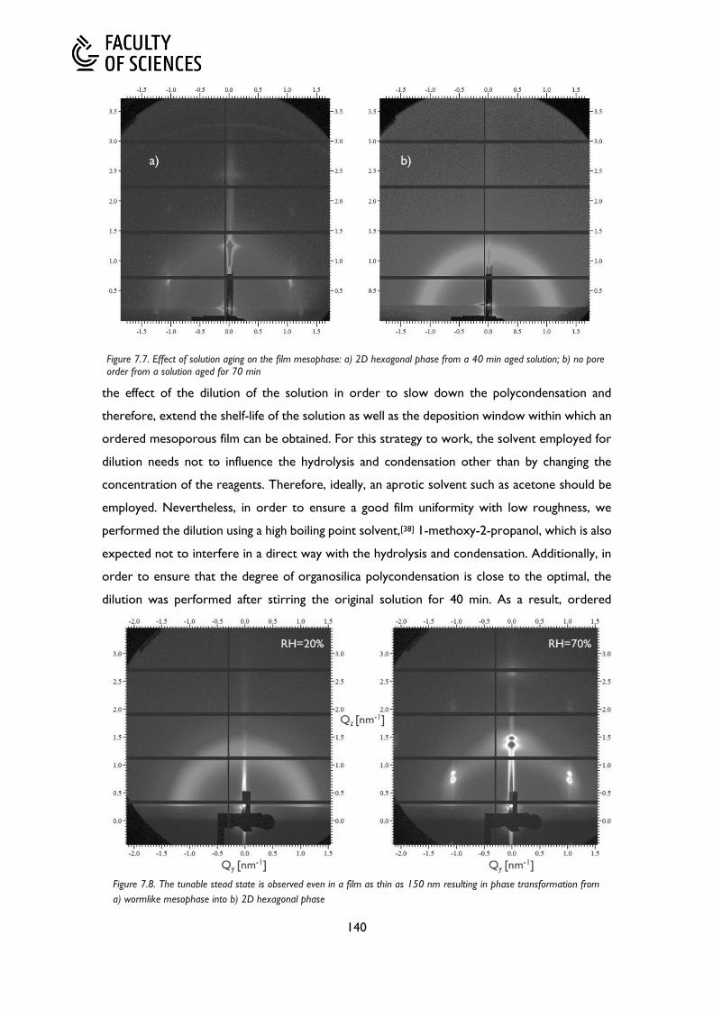
140
the effect of the dilution of the solution in order to slow down the polycondensation and
therefore, extend the shelf-life of the solution as well as the deposition window within which an
ordered mesoporous film can be obtained. For this strategy to work, the solvent employed for
dilution needs not to influence the hydrolysis and condensation other than by changing the
concentration of the reagents. Therefore, ideally, an aprotic solvent such as acetone should be
employed. Nevertheless, in order to ensure a good film uniformity with low roughness, we
performed the dilution using a high boiling point solvent,[38] 1-methoxy-2-propanol, which is also
expected not to interfere in a direct way with the hydrolysis and condensation. Additionally, in
order to ensure that the degree of organosilica polycondensation is close to the optimal, the
dilution was performed after stirring the original solution for 40 min. As a result, ordered
Figure 7.8. The tunable stead state is observed even in a film as thin as 150 nm resulting in phase transformation from
a) wormlike mesophase into b) 2D hexagonal phase
Figure 7.7. Effect of solution aging on the film mesophase: a) 2D hexagonal phase from a 40 min aged solution; b) no pore order from a solution aged for 70 min
a) b)

141
mesophase was observed for films as thin as 150 nm. Importantly, the tunable steady state (TSS)
exists in films as thin as 150 nm. The thinner the films the faster they are expected to dry during
spin-coating and therefore their matrices are expected to condense faster and probably shorten
the window of the TSS. Nevertheless, the phase transformation (Figure 7.8) observed for the
150 nm film shows that the polycondensation is not complete more than 5 min after the spinning
which is when the first GISAXS patterns are obtained. Also, the phase transformation shown at
Figure 7.8 occurred after about 120 min solution aging showing that the deposition window
which allows obtaining ordered PMO has been extended. Another deposition following 200 min
of solution aging also resulted in a GISAXS pattern indicative of a 2D hexagonal mesophase (not
shown). The dilution experiments were also performed on a 20 min aged solution but the
lamellar-to-3D-hexagonal phase transformation was not observed after the dilution. However,
the latter was not due to the dilution but rather due to an aged (probably, hydrolyzed) precursor
which is discussed next.
The organosilica precursor is sensitive to the ambient atmosphere. A freshly open bottle of
organosilica precursor was used to obtain the results reported here. However, the use of a
precursor from a bottle which was opened two months earlier did not allow us to reproduce
the reported results. At RH=70%, it resulted in a Debye ring indicating a disordered wormlike
phase rather than the 3D hexagonal phase demonstrated earlier. This observation implies a
precursor aging effect due to the precursor sensitivity to moisture which can cause hydrolysis,
as previously described for other alkoxysilicates.[18] No evidence of a hydrolysis was observed
for the organosilica precursor in the bottles opened within the three days’ timeframe of the
GISAXS experiments at ELETTRA.
Due to the use of CTAC in these syntheses, the films are not completely hydrophobic. The
hydrophilicity of the films is evident from the FTIR spectrum shown in Figure 7.9. The spectrum
contains a sharp peak at 3735 cm-1 indicating the presence of isolated silanol groups which need
to be silylated in order to obtain a hydrophobic film. Furthermore, a peak at 1360 cm-1 reveals
Figure 7.9. FTIR spectrum containing the characteristic bands observed for all
of the PMO films described in this chapter

142
the presence of intact methylene groups. Importantly, the peak around 1260 cm-1 is broader
than a typical Si-CH3 peak. Therefore, it can be peak-fitted by two Gaussian peaks centered at
1275 and 1265 cm-1. The peak at 1275 cm-1 corresponds to the C-H vibration in (R3SiO)3SiCH3
T groups while the one at 1265 cm-1 to a (R3SiO)2Si(CH3)2 D groups. Figure 7.10 shows the
sequence of self-hydrophobization reactions which result in the formation of D groups from
silicon atom bonded to two methylene groups as is the case in the ring precursor. The presence
of D groups reduces significantly the average connectivity number, which is the number of
network forming bonds per networked atom, of the organosilicate matrix.[39] A connectivity
number lower than 2.4 is below the percolation of rigidity which means that the mechanical
stability is compromised. It has been shown that if each Si atom had three network-forming
bonds and one bond to a methyl group, i.e. T groups, then a connectivity number of 2.4 would
be reached.[39] Therefore, in order to achieve optimal mechanical properties, the formation of
D groups should be avoided. Nevertheless, the peak-fitting of the band at ca. 1270 cm-1 reveals
that the concentration of the D groups is higher than the concentration of T groups. Therefore,
the ring precursor seems not to be a suitable precursor when an optimization of the low-k
mechanical properties is needed. However, a complication of this analysis is that since each
silicon atom is bonded to two methylene groups, upon a self-hydrophobization reaction, the
formed functionality is also a D group but one where the silicon is bonded to two siloxane, one
methylene and one methyl functionalities. Such D groups are equivalent to a T group in terms
of a contribution to the average connectivity number. Unfortunately, it is not clear whether the
two types of D groups can be distinguished by an FTIR analysis.
An evaluation of the Young’s moduli of the films described in this chapter (points in Figure 7.11)
reveals that the films possess inferior mechanical properties when compared to oxycarbosilane
films from literature in which no pore order was present (line in Figure 7.11).[40] These
oxycarbosilane films have been obtained from a methylene-bridged precursor but one that does
not allow the formation of D groups, i.e. the BTESM. Therefore, the lower YM observed for our
films might be due to a lower matrix connectivity as compared to those in literature. Another
factor which is very likely to contribute to the observed difference is the fact that Dubois et al.
annealed their films at 450°C while we annealed the PMOs at the more compatible with the
Figure 7.10. The self-hydrophobization sequence which results in the formation of D, (R3SiO)2Si(CH3)2, groups: a) Si atom bonded to two methylene groups with two silanols in proximity; b) one self-hydrophobizatoin results in a D group where the
Si is bonded to methylene and methyl group; c) second self-hydrophobization leads to a D group where the Si is bonded to
two methyl groups

143
BEOL processing temperature of 400°C. The higher anneal temperature of 450°C certainly
results in higher silanol condensation and consequently, potentially higher matrix connectivity.
However, the PMO films are expected to achieve higher YM values due to their ordered
pores.[10] While it is difficult to make a conclusion on the effect of the pore order on the YM
when comparing with results in literature due to experimental differences, when we compare
to films with disordered porosity obtained in our laboratory (to be presented in the next
chapter), we do not see a clear benefit to the YM from the ordered porosity. Nevertheless, the
latter is probably due to the limited pore order observed in our PMO films (Figure 7.4 and Figure
7.6). Therefore, further efforts to increase the size of the domains with ordered pores and
ultimately obtain a monocrystal-like PMO are necessary in order to be able to draw a more
reliable conclusion about the effect of the pore organization on the YM.
7.4. Conclusions
In summary, we have demonstrated, for the first time, the existence of a tunable steady state in
PMO spin-coated films. Therefore, we stressed the importance of the ambient relative humidity
at which an as-deposited film is aged. Controlling the aging conditions, we were able to obtain
films with 3D or 2D hexagonal phases depending on the surfactant to organosilica molar ratio.
Additionally, in the context of the charge density matching mechanism, we demonstrated the
competing effects of the adsorbed H2O molecules on the mesophase determination. The
interaction between the H2O and CTAC molecules leads to an increase of the micelle surface
curvature; in the meantime, the H2O molecules can cause depolymerization of the siloxane
bonds creating conditions which favor the decrease of the micelle surface curvature.
Furthermore, we emphasized the importance of the polycondensation degree of the organosilica
oligomers by demonstrating different mesophases as a function of the solution aging, i.e. 3D
hexagonal after 20 min, 2D hexagonal after 40 min aging and no ordered mesophase if the
solution is aged for longer than 70 min. Additionally, GISAXS patterns tentatively attributed to
cubic mesophases were observed when the water to organosilica molar ratio was reduced from
30 to 14. Notably, the TSS exists in spin-coated films as thin as 150 nm more than 5 min after
Figure 7.11. Comparison of the YM of the obtained PMO films (points)
to oxycarbosilane films[40](line) in which no pore order has been observed

144
the deposition. Finally, the deposition window which makes possible obtaining films with an
ordered mesophase can be extended by at least 160 min by diluting the solution with a suitable
solvent.
7.5. References
[1] Z. Chen, Y. Jiang, D. R. Dunphy, D. P. Adams, C. Hodges, N. Liu, N. Zhang, G. Xomeritakis,
X. Jin, N. R. Aluru, S. J. Gaik, H. W. Hillhouse, C. J. Brinker, Nat. Mater. 2010, 9, 667.
[2] M. Etienne, A. Quach, D. Grosso, L. Nicole, C. Sanchez, A. Walcarius, Chem. Mater. 2007,
19, 844.
[3] A. Walcarius, E. Sibottier, M. Etienne, J. Ghanbaja, Nat. Mater. 2007, 6, 602.
[4] T. C. Wei, H. W. Hillhouse, Langmuir 2007, 23, 5689.
[5] C. H. Ko, J. M. Kim, R. Ryoo, Microporous Mesoporous Mater. 1998, 21, 235.
[6] R. Ryoo, C. H. Ko, S. J. Cho, J. M. Kim, J. Phys. Chem. B 1997, 101, 10610.
[7] Y. Hu, A. Bouamrani, E. Tasciotti, L. Li, X. Liu, M. Ferrari, ACS Nano 2010, 4, 439.
[8] H. Lian, Y. Liang, Y. Yamauchi, K. C. Wu, J. Phys. Chem. 2011, 115, 6581.
[9] D. J. Michalak, J. M. Blackwell, J. M. Torres, A. Sengupta, L. E. Kreno, J. S. Clarke, D.
Pantuso, J. Mater. Res. 2015, 30, 3363.
[10] D. Jauffrès, R. Dendievel, M. Verdier, Thin Solid Films 2011, 520, 430.
[11] D. Grosso, F. Ribot, C. Boissiere, C. Sanchez, Chem. Soc. Rev. 2011, 40, 829.
[12] L. Nicole, C. Boissière, D. Grosso, A. Quach, C. Sanchez, J. Mater. Chem. 2005, 15, 3598.
[13] D. Grosso, F. Babonneau, P. Albouy, H. Amenitsch, A. R. Balkenende, A. Brunet-Bruneau,
J. Rivory, Chem. Mater. 2002, 14, 931.
[14] A. Gibaud, D. Grosso, B. Smarsly, A. Baptiste, J. F. Bardeau, F. Babonneau, D. A. Doshi, Z.
Chen, C. J. Brinker, C. Sanchez, J. Phys. Chem. B 2003, 107, 6114.
[15] F. Cagnol, D. Grosso, G. J. de A. A. Soler-Illia, E. L. Crepaldi, F. Babonneau, H. Amenitsch,
C. Sanchez, J. Mater. Chem. 2003, 13, 61.
[16] D. Grosso, F. Cagnol, G. J. de A. A. Soler-Illia, E. L. Crepaldi, H. Amenitsch, A. Brunet-
Bruneau, A. Bourgeois, C. Sanchez, Adv. Funct. Mater. 2004, 14, 309.
[17] D. Grosso, F. Babonneau, C. Sanchez, G. J. de A. A. Soler-Illia, E. L. Crepaldi, P. A. Albouy,
H. Amenitsch, A. R. Balkenende, A. Brunet-Bruneau, J. Sol-Gel Sci. Technol. 2003, 26, 561.
[18] M. P. Tate, V. N. Urade, S. J. Gaik, C. P. Muzzillo, H. W. Hillhouse, Langmuir 2010, 26,
4357.
[19] A. Grunenwald, A. Ayral, P.-A. Albouy, C. Licitra, P. Gergaud, D. Quemener, A. Deratani,
V. Rouessac, A. Zenasni, V. Jousseaume, Microporous Mesoporous Mater. 2012, 150, 64.
[20] J. Zhang, G. Zhang, Y. Gao, R. Sun, C. P. Wong, J. Mater. Sci. 2016, 51, 7966.

145
[21] T. Jiang, S. J. Ding, Z. Y. Fan, W. Zhang, Adv. Mater. Res. 2014, 887–888, 757.
[22] W. Wang, D. Grozea, S. Kohli, D. D. Perovic, G. A. Ozin, ACS Nano 2011, 5, 1267.
[23] M. Seino, W. Wang, J. E. Lofgreen, D. P. Puzzo, T. Manabe, G. A. Ozin, J. Am. Chem. Soc.
2011, 133, 18082.
[24] S. S. Park, M. Santha Moorthy, C.-S. Ha, NPG Asia Mater. 2014, 6, e96.
[25] P. Van der Voort, D. Esquivel, E. De Canck, F. Goethals, I. Van Driessche, F. J. Romero-
Salguero, Chem. Soc. Rev. 2013, 42, 3913.
[26] M. A. Wahab, J. N. Beltramini, RSC Adv. 2015, 5, 79129.
[27] M. Aliofkhazraei, Comprehensive guide for mesoporous materials, Volume 4: Application
and Commercialization; Aliofkhazraei, M., Ed.; Nova Science Publishers, Inc.: New York,
2015.
[28] J. G. Croissant, X. Cattoën, J.-O. Durand, M. Wong Chi Man, N. M. Khashab, Nanoscale
2016, 8, 19945.
[29] W. Wang, J. E. Lofgreen, G. A. Ozin, Small 2010, 6, 2634.
[30] K. Landskron, B. D. Hatton, D. D. Perovic, G. A. Ozin, Science 2003, 302, 266.
[31] M. P. Tate, V. N. Urade, J. D. Kowalski, T. C. Wei, B. D. Hamilton, B. W. Eggiman, H. W.
Hillhouse, J. Phys. Chem. B 2006, 110, 9882.
[32] M. Cypryk, Y. Apeloig, Organometallics 2002, 21, 2165.
[33] A. Monnier, F. Schüth, Q. Huo, D. Kumar, D. Margolese, R. S. Maxwell, G. D. Stucky, M.
Krishnamurty, P. Petroff, A. Firouzi, M. Janicke, B. F. Chmelka, Cooperative formation of
inorganic-organic interfaces in the synthesis of silicate mesostructures. Science 1993,
261, 1299–303.
[34] Q. Huo, D. I. Margolese, U. Ciesla, P. Feng, T. E. Gier, P. Sieger, R. Leon, P. M. Petroff, F.
Schüth, G. D. Stucky, Nature 1994, 368, 317.
[35] A. Firouzi, D. Kumar, L. Bull, T. Besier, P. Sieger, Q. Huo, S. Walker, J. Zasadzinski, C. Glinka,
J. Nicol, A. Et, Science (80-. ). 1995, 267, 1138.
[36] S. H. Tolbert, C. C. Landry, G. D. Stucky, B. F. Chmelka, P. Norby, J. C. Hanson, A. Monnier,
Chem. Mater. 2001, 13, 2247.
[37] C. J. Brinker, J. Non. Cryst. Solids 1988, 100, 31.
[38] H. Kozuka, Y. Ishikawa, N. Ashibe, J. Sol-Gel Sci. Technol. 2004, 31, 245.
[39] A. D. Ross, K. K. Gleason, J. Appl. Phys. 2005, 97, 113707.
[40] G. Dubois, W. Volksen, T. Magbitang, R. D. Miller, D. M. Gage, R. H. Dauskardt, Adv.
Mater. 2007, 19, 3989.

146

147
CHAPTER 8. PERIODIC MESOPOROUS ORGANOSILICA
FILMS FOR LOW-K APPLICATION: PROMISES AND
CHALLENGES
As we have shown in Chapter 7, the synthesis of 2D hexagonal PMO films using
cetyltrimethylammonium chloride (CTAC) is independent of the ambient conditions during
deposition. Therefore, it is the most compatible with IC manufacturing. Nevertheless, we show
that the PMO films with a 2D hexagonal pore organization have 1.7 GPa lower Young’s modulus
than a film with disordered porosity at a dielectric constant of 2.30. Furthermore, CTAC is an
ionic surfactant and ionic surfactants are considered detrimental to the low-k’s electrical
reliability. However, we demonstrate CTAC-templated PMO low-k films with low leakage
current of 1.6x10⁻⁹ A/cm2 at 1 MV/cm and a breakdown field of 5.5 MV/cm both of which are
comparable to low-k films reported in literature. Additionally, we discuss challenges depositing
the PMO films in 45 nm trenches. We demonstrate that the high surface energy of the substrate
is important in order to obtain ordered porosity.

148
8.1. Introduction
Periodic mesoporous organosilica (PMO) films are considered to be a promising low-k candidate
for future generation ultra-large scale integration. Compared to the traditional low-k films, one
of the main advantages of the PMOs is the control over the pore structure and the ability to
obtain an ordered porosity. The films with ordered porosity have been shown theoretically[1–3]
and experimentally[4] to possess an improved Young's modulus as compared to films with
disordered pores. An additional advantage of the PMO films is that porosity values higher than
50% without a pore collapse can be obtained.[5] Finally, PMOs have been shown to self-
hydrophobize at T>300°C[6] and we have shown that the process initiates at even lower
temperatures (Chapter 5). The self-hydrophobization can result in a hydrophobic film which is
stable against moisture adsorption[7,8] and therefore with stable dielectric properties against
atmospheric effects without the need for an additional hydrophobization treatment.
In order to deduce the effect of the pore organization on the film properties, it is beneficial to
be able to obtain films with ordered and disordered pore organizations from the same solution.
In contrast, films obtained as a result of differing processing conditions might result in a differing
hydrolysis and condensation kinetics leading to significantly different organosilicate oligomer
distribution affecting the observed film properties. For instance, it has been shown that the
abundance of small 3-memebred siloxane rings in the film would lead to a film with higher elastic
modulus as compared to a film with larger siloxane cyclic species.[4] Even less reliable and
challenging would be to attempt to deduce the role of the pore order between films obtained
via sol-gel and PECVD, for instance, because of the extensive bond rearrangement characteristic
of the PECVD method. Therefore, in this study, we compare films obtained from the same
solution but having different pore organization (mesophase).
Ionic surfactants are considered incompatible with microchip manufacturing.[9] Even though no
elaboration has been provided for why they are unsuitable, it is probably due to an expected
detrimental effect on the electrical reliability of the low-k films obtained using an ionic surfactant.
Nevertheless, it has been demonstrated that the addition of a salt as a catalyst, part of which
inevitably gets incorporated in the final film, results in low-k films with good electrical
reliability.[10] However, the amounts of catalyst in the solution were 30 wt ppm or lower which
is expected to be much lower than the remaining ions if an ionic surfactant is employed as a
structure-directing agent (SDA). Indeed, Ting et al.[11] have reported that the use of the ionic
surfactant cetyltrimethylammonium bromide (CTAB) leads to porous films with a leakage
current density so high that they could not quantify it with the available equipment. Additionally,
in contrast to the films templated by non-ionic surfactants, they showed a positive flat-band
voltage (VFB) for the low-k film templated by CTAB which was attributed to the abundance of
remaining Br- ions. Nevertheless, in that study, there are several observations which have not

149
been observed in the films prepared in our laboratory. For instance, the authors have reported
a very high refractive index of 1.428 for a film with a pore volume of 42% which they have
attributed to the ionic contribution to the dielectric function of the Br- ions in the film even if
an ionic response is usually not expected in the optical frequency range.[12] In comparison, we
have obtained films with a similar pore volume and their refractive index is ca. 1.255.
Additionally, in a previous study detailed in Chapter 4, we showed that the VFB of the low-k films
templated by an ionic surfactant was negative similar to the films templated by a non-ionic
surfactant indicating the lack of a significant contribution from the chlorine ions to the VFB. Given
that the ionic surfactants are the SDAs which result in the mesoporous films with the smallest
pore diameter of about 2 nm, it is important to clarify whether the ionic surfactants are indeed
incompatible with the back-end of line processing and whether they deteriorate the low-k
reliability. Therefore, we evaluated the electrical reliability of PMO films templated with an ionic
surfactant in comparison to a non-ionic surfactant and to a commercial k2.2 spin-on film by
performing current-voltage (I-V) measurements of a PMO low-k deposited in a 45 nm trench. In
order to achieve the latter, we took advantage of a low-k replacement integration scheme which
allows[13] avoiding the plasma-induced damage which is one of the biggest challenges for the
integration of porous low-k dielectrics and therefore, allows studying the intrinsic low-k
properties in technologically relevant structures and dimensions.
8.2. Experimental Section
The coating solution was synthesized using a modified synthesis procedure of Landskron et al.[14]
In a typical synthesis ethanol (1.44 ml), HCl (0.71 ml 10-3M), cetyltrimethylammonium chloride
(0.85 ml 25% aqueous solution), and 1,1,3,3,5,5-hexaethoxy-1,3,5-trisilacyclohexane (0.93 ml)
were mixed and stirred at room temperature. Following the stirring, the solution was spin-
coated at 2500 rpm for 60 s on a 100 Si substrate on which a native oxide had been grown. The
deposition was performed from the same solution following an aging at RT for 50 min and 100
min. The films were deposited at a lab humidity which was not actively controlled and is usually
in the range between 40 and 50%. Finally, the CTAC was thermally decomposed at 400°C in an
inert N2 atmosphere for 2 h.
Alternatively, PMO films were deposited on a patterned structure which was obtained following
the processing procedure shown schematically in Figure 8.1. The details of the processing steps
can be found elsewhere.[13,15] In short, instead of a low-k, a sacrificial “template” is deposited and
Figure 8.1. The template-replacement integration scheme

150
patterned which is followed by the copper electroplating and polishing. Thus far, these steps
describe the usual damascene integration processing. Next, the template is removed by a plasma
processing optimized not to oxidize the exposed metal and thin metal barrier. As a result,
“standing” metal lines are obtained with gaps which can be filled with the ultra-low-k film. Three
gap sizes are available – 45, 50, and 55 nm. The height of the metal lines is about 85 nm. The
effect of the surface energy of SiCN, the interface on which the PMO is deposited, on the PMO
film was investigated. The gap fill structures on which 6 nm SiCN had been deposited was
exposed to a short CO2 plasma in order to increase the surface energy of the SiCN. The
deposition on a hydrophilized SiCN mimics the deposition on the hydrophilic SiO2 reported in
the previous chapters, i.e. by creating similar surface energy conditions, the surfactant self-
assembly is ensured to be reproduced. Alternatively, the high surface energy SiCN was
additionally treated with the vapors of the silylation agent dimetilaminotrimethylsilane
(DMATMS) at 250°C in order to obtain a low surface energy SiCN.
To compare the stress-induced leakage current (SILC) density between PMO low-k films
templated by an ionic and a non-ionic surfactant, we deposited a CTAC-templated and a BrijS10-
templated PMO films in the gap-fill structures. Instead of 2 hours, the as-deposited films were
annealed for only 20 min in order to avoid potential oxidation of the Cu lines with the longer
annealing at 400°C. The films were additionally silylated by a vapor phase exposure to DMATMS
at 250°C in order to exclude the detrimental effect on the leakage current of the Si-OH groups
present in the PMO film templated by the ionic surfactant.
8.3. Results and Discussion
8.3.1. Effect of pore order on Young’s modulus
As shown in Chapter 7, the synthesis procedure described in the experimental section results
in a 2D hexagonal film if the solution is aged for longer than 40 min but shorter than 70 min.
Also, the pore organization is relatively independent of ambient humidity which for these
experiments could not be controlled precisely. On the other hand, if the solution is aged for 70
min or longer then a film with a disordered worm-like pore organization is obtained. The
difference in pore organization was established by XRD and GISAXS (Figure 8.2). Additionally,
a TEM investigation of the film with ordered porosity revealed a long range order (Figure 8.3a)
which is punctuated by relatively small disordered regions which separate domains of ordered
pores with different orientations (Figure 8.3b). Both of the domains with ordered channels in
Figure 8.3b) seem to belong to the p6mm space group oriented parallel to the substrate but
they are oriented perpendicular to each other. The disordered pore organization in the film
aged for 100 min can be deduced from the GISAXS pattern shown in Figure 8.2 b) where no

151
diffraction spots are observed but only a Debye ring indicating the wormlike pore structure
characterized by a narrow pore size distribution similar to the films with ordered porosity.
Due to the similar synthesis conditions, the films being compared have a very similar pore size
with a diameter centered on 2 nm calculated from the toluene adsorption isotherms (not
shown). Importantly, comparing films obtained from the same solution ensures that there are
no significant differences in the size distribution of the siloxane oligomers. Therefore, the films
are expected to have similar to each other matrix connectivity which is known to affect the
Young’s modulus.[16] Admittedly, the fact that following a 50 min solution aging, a film with
ordered pores is obtained while a longer aging results in wormlike pores indicates that there
are differences in the siloxane oligomer size. Nevertheless, in both cases, the shared pH of ca.
3.0 favors the formation of weakly branched oligomers which grow longer with the solution
aging time.[17] Furthermore, the annealing at 400°C following the deposition removes any
differences in the siloxane population in the final ordered and disordered films. This conclusion
Figure 8.3. TEM micrographs showing a) the well-ordered 2D hexagonal pore organization in the film obtained from a
solution aged for 50 min and b) the ordered pores are organized in domains as a result of which some channels are
perpendicular to others
Figure 8.2. GISAXS patterns showing the a) 2D hexagonal organization in the film obtained from a solution aged for 50
min and b) the wormlike pore organization in the film obtained from the same solution aged for 100 min

152
is based on the films’ FTIR spectra (Figure 8.4) in the region between 900 and 1250 cm-1 which
contains information about the distribution of siloxane bond angles and lengths which vary
among the various cyclic siloxane units. In this region, the spectra overlap showing that the
organosilica matrices of the films are composed to a large extent of the same bond
configurations.
A drawback of the current experimental design is that the porous films have different densities
due to the lower surfactant incorporation in a more polycondensed gel. Indeed, compared to
the film with ordered porosity, the disordered porosity film has 0.05 g/cm3 higher density,
deduced form XRR measurements, and 3.5 percentage points lower open porosity, calculated
from toluene EP measurements (Figure 8.5a). As a result, the observed difference in Young’s
modulus is partly explained by the difference in density. In particular, the film with a 2D
hexagonal pore organization, which is also the more porous film, has a YM 1.7 GPa lower than
the film with wormlike pores. When compared with literature where systematic syntheses and
characterization of YM as a function of density were performed,[18,19] the density difference
seems to explain about half of the difference in YM that we observe. In order to explain the
remaining difference, we take into account the anisotropy characteristic of films with a pore
organization belonging to a wallpaper space group such as the p6mm. In films with p6mm pore
order in which the pores are parallel to the substrate, it is well-known that the axis normal to
the substrate is the weakest mechanically.[5] Furthermore, the nanoindentation, employed to
Figure 8.4. FTIR spectra of the films obtained following 50 and 100 min
solution aging.
Figure 8.5. A comparison of low-k properties as a function of pore organization

153
obtain the elastic modulus, provides information mainly about the mechanical properties normal
to the substrate.[20] On the other hand, the film with disordered pores is expected to have
largely isotropic mechanical properties. Therefore, effectively, we are comparing the weakest
YM component of the film with the ordered pores to the average elastic response of the film
with disordered pores. Consequently, for the same density, we would expect a higher YM for
the film with disordered pores than for the film with 2D hexagonal pores. Employing FEM
calculations, Michalak et al.[5] have shown (FIG. 13 in ref.[5]) that a film with random spheroid
pores would have a higher YM than the transverse YM components of the ordered porosity
film. At a porosity of ca. 55%, the disordered porosity film has about 2 GPa higher YM than the
YM component normal to the substrate. Nevertheless, the YM component parallel to the
channels can be three times higher than each of the transverse components, 15 vs 5 GPa (FIG.
13 in ref.[5]). Therefore, the lower YM for the ordered film as compared to the disordered seems
reasonable even if on average the YM of the ordered porosity film is expected to be higher than
that of a disordered porosity film. However, these results seem to contradict a previous report
where employing nanoindentation, films with hexagonally ordered pores were reported to have
a significantly higher YM as compared to a film with a disordered porosity.[4]
The small difference in density between the films obtained from a 50 min and a 100 min aged
solution results in a small difference in the dielectric constant. When the capacitance of a metal-
insulator-semiconductor (MIS) structure is measured at room temperature at 100 kHz,[21] a k
value of 2.30 is calculated for both of the films. When the capacitance measurement is performed
at 200°C at 100 kHz, ensuring the evaporation of any physisorbed water, k-values of 2.27 and
2.29 are calculated for the films obtained from a 50 and 100 min aged solution, respectively. The
difference with the value obtained at room temperature is not statistically significant indicating
that the hydrophilicity of the films, reported in Chapter 7, has not led to a significant
physisorption of moisture within the one week storage duration in a clean room environment.
8.3.2. PMO film deposition in 45 nm trenches
A PMO film with larger ordered domains is obtained when the film is deposited on a hydrophilic
SiCN rather than a hydrophobic SiCN. The latter was deduced from an XRD study of the PMO
film deposited on a hydrophilic and a hydrophobic SiCN (Figure 8.6). The diffraction peak from
the film deposited on the hydrophilic SiCN is about 10 times more intense than if the coating
solution is spun on a hydrophobic SiCN. Additionally, the full-width-at-half-maxima (FWHM) are
0.21° and 0.10° when the SiCN is hydrophobic and hydrophilic, respectively. According to
Scherrer’s formula,[22] the smaller FWHM indicates the larger ordered domains in the film
deposited on the hydrophilic SiCN. The difference in pore organization can also be seen in the
TEM images in Figure 8.7. The higher quality of the PMO on the hydrophilic SiCN can clearly be
seen. Nevertheless, the pore order is disrupted in the space between the metal lines where no

154
clear pore organization is observed (Figure 8.7 a). Additionally, since the hydrophobized SiCN
does not have any anchoring chemical functionalities to which the PMO can adhere, the film
shrinkage during the thermal template removal causes delamination of the PMO from both the
side-walls and the bottom of the trench (Figure 8.7 b). Therefore, it is important to ensure the
presence of –OH groups on the substrate when the PMO is deposited in terms of both adhesion
and pore organization.
To understand why the pore order is disrupted between the metal lines we examined wider
gaps on the gap-fill structure. The hydrophilic SiCN is beneficial for the pore order since both
on the Cu lines and between the Cu lines in the 450 nm gap, the pores immediately on top of
the SiCN are not disrupted (Figure 8.8). On the other hand, next to the sidewalls of the metal
lines, no pore order is observed. Therefore, the surface energy of the sidewalls seems to be
disrupting the pore order and as a result, disordered pore regions of at least 25 nm to the left
and the right of the metal lines are created (Figure 8.8b). This is why no ordered porosity is
observed in the narrow 45 nm trenches. Two possible explanations are considered. First, the
disordered pores next to the sidewalls might be due to a different surface energy at the sidewall
as compared to the surface of the trenches. The differing surface energy might be due to a non-
Figure 8.7. TEM micrographs showing the gap-fill structures deposited with PMO on a) hydrophilic SiCN and b) hydrophobic
SiCN
Figure 8.6. XRD diffractograms showing the better ordered PMO film
on the hydrophilic SiCN as compared to the hydrophobic SiCN

155
conformal SiCN deposition which does not cover fully the sidewalls.[15] As a result, the sidewalls
consist of an oxidized TaN. Second, the disordered porosity might be the result of the topology.
In particular, the sidewalls might promote the tubular micelles to grow perpendicular to the
silicon substrate, i.e. parallel to the walls. However, no such alignment is observed, probably,
due to the conflicting driving force for the micelle to align parallel to the substrate. As a result,
the conflicting driving forces lead to disordered porosity.
8.3.3. Effect of the template on the electrical reliability of PMO films
The current-voltage (I-V) curves shown in Figure 8.9 reveal that following the thermal template
removal, in the PMO film, there are numerous leakage paths which lead to a wide distribution
of breakdown fields (EBD) from 2.8 to 5.7 MV/cm. The shown I-V curves are those observed for
the BrijS10-templated film but the CTAC-templated film display a similar response. However, a
consequent silylation improves the I-V behavior by eliciting a more consistent leakage current
density as a function of the applied electric field. Therefore, the leakage paths before the silylation
are attributed to the presence of Si-OH groups. According to the Poole-Frenkel emission
mechanism,[23] under an applied electric field, the Coulomb potential energy of the proton from
the silanol groups is reduced increasing the probability that the bound proton will become free
Figure 8.8. Comparison of the pore order in gaps of a) 45 and b) 450 nm
Figure 8.9. Stress-induced leakage current for a PMO a) annealed at 400°C for 20 min and b) additionally silylated by DMATMS.
The inset in a) shows schematically the metal lines and the contact pads. The inset in b) shows the trimethylsilane functionality
which gets incorporated into the films as a result of the silylation treatment

156
and contribute to the leakage current. The leakage current has been further shown to increase
with the higher amount of adsorbed water[24] which is facilitated by the presence of the Si-OH
groups. The silylation replaces the O-H groups with C-H-terminating functionalities. In spite of
the fact that the C-H bond has a smaller dissociation energy as compared to the O-H, the methyl
functionalities prevent the water adsorption which has a major role in the proton conduction
contributing to the leakage current.[24] Similarly, the EBD distribution becomes narrower, i.e.
between 5.1 and 7.0 MV/cm as compared to the EBD before the silylation and its average value
increases from 4.2 to 6.3 MV/cm. Therefore, the next comparisons between the films templated
by the ionic and non-ionic surfactants are for silylated films.
Following the hydrophobization treatment, the CTAC-templated film has a lower breakdown
field of 5.7 MV/cm than the BrijS10-templated film which has an EBD of 6.3 MV/cm (Figure 8.10).
At a high electric field, E=4 MV/cm, the leakage current is about two times larger, 1.8x10⁻³ A/cm2,
for the film templated by the ionic surfactant as compared to the film templated by the non-
ionic template. Nevertheless, it is comparable to the leakage current observed in the commercial
spin-on SOG2.2 low-k. On the other hand, the leakage current measured for the CTAC-
templated PMO at 1 MV/cm of 1.6x10⁻⁹ A/cm2 is close to the tool’s sensitivity level and an order
lower than that of the BrijS10-templated film. These observations differ from a previous report
where the use of an ionic surfactant, CTAB, resulted in films with very high leakage current.[11]
The high leakage was attributed to the presence of excessive amount of bromine ions following
the template removal. Therefore, we compared the chlorine content in the BrijS10- and CTAC-
templated films. Indeed, there is on average about 3 to 4 times more chlorine in the CTAC-
templated film as compared to the BrijS10-templated (Figure 8.10 b). The source of chlorine
ions in the BrijS10-templated film is the HCl acid catalyst. Consequently, while we have
ascertained the presence of chlorine ions in the CTAC-templated film, the observed I-V curves
demonstrate that the ions do not deteriorate significantly the electrical reliability. Therefore, in
terms of dielectric reliability, the ionic surfactants are a suitable templating agent for PMO films
intended for a low-k application.
Figure 8.10. Films templated by ionic and non-ionic surfactants: a) comparison of the SILC; b) ToF-SIMS results showing the
difference in Cl- content in the CTAC and BrijS10-templated films
a) b)

157
8.4. Conclusions
A PMO film with a 2D hexagonal pore order has been shown to possess 1.7 GPa lower Young’s
modulus than a film with a disordered porosity. This has been explained by a small difference in
density and by the anisotropy of the PMO with a 2D hexagonal mesophase. A comparison of
the electrical reliability of PMO films templated by an ionic surfactant, CTAC and a non-ionic
surfactant, BrijS10, demonstrates that the CTAC is a suitable templating agent for low-k films.
The use of CTAC does not result in a significantly higher leakage current density or lower
breakdown field when compared to the film with a non-ionic surfactant. In particular, the leakage
current density of the CTAC-templated film at 1MV/cm is 1.6x10⁻⁹ A/cm2 while the breakdown
field is 5.7 MV/cm. At the same time, CTAC-templated PMO films have a small pore size of
about 2 nm and a narrow pore size distribution both of which are very important for a low-k
application. High surface energy of the substrate is shown to be required in order to obtain a
well-ordered PMO and reduce the size and number of domains with disordered porosity. The
latter is not expected to affect the electrical properties, e.g. permittivity and reliability, but it will
result in variability in the mechanical properties, to the extent that they are determined by the
pore organization.
8.5. References
[1] H. Miyoshi, H. Matsuo, Y. Oku, H. Tanaka, K. Yamada, N. Mikami, S. Takada, N. Hata, T.
Kikkawa, Jpn. J. Appl. Phys. 2004, 43, 498.
[2] H. Miyoshi, K. Yamada, K. Kohmura, N. Fujii, H. Matsuo, H. Tanaka, Y. Oku, Y. Seino, N.
Hata, T. Kikkawa, Japanese J. Appl. Physics, Part 1 Regul. Pap. Short Notes Rev. Pap. 2005,
44, 5982.
[3] D. Jauffrès, R. Dendievel, M. Verdier, Thin Solid Films 2011, 520, 430.
[4] H. Fan, C. Hartshorn, T. Buchheit, D. Tallant, R. Assink, R. Simpson, D. J. Kissel, D. J. Lacks,
S. Torquato, C. J. Brinker, Nat. Mater. 2007, 6, 418.
[5] D. J. Michalak, J. M. Blackwell, J. M. Torres, A. Sengupta, L. E. Kreno, J. S. Clarke, D.
Pantuso, J. Mater. Res. 2015, 30, 3363.
[6] T. Asefa, M. J. MacLachlan, H. Grondey, N. Coombs, G. A. Ozin, Angew. Chemie Int. Ed.
2000, 39, 1808.
[7] F. Goethals, I. Ciofi, O. Madia, K. Vanstreels, M. R. Baklanov, C. Detavernier, P. Van Der
Voort, I. Van Driessche, J. Mater. Chem. 2012, 22, 8281.
[8] W. Wang, D. Grozea, S. Kohli, D. D. Perovic, G. A. Ozin, ACS Nano 2011, 5, 1267.
[9] G. Dubois, W. Volksen, In Advanced Interconnects for ULSI Technology; John Wiley &
Sons, Ltd: Chichester, UK, 2012; pp. 1–33.

158
[10] T. Kikkawa, Y. Kayaba, K. Kohmura, S. Chikaki, IEEE Int. Reliab. Phys. Symp. Proc. 2011,
130.
[11] C.-Y. Ting, H.-S. Sheu, W.-F. Wu, B.-Z. Wan, J. Electrochem. Soc. 2007, 154, G1.
[12] P. S. Ho, J. Leu, W. W. Lee, Low Dielectric Constant Materials for IC Applications; Ho, P.
S.; Leu, J.; Lee, W. W., Eds.; Springer-Verlag Berlin Heidelberg 2003, 2003.
[13] L. Zhang, J.-F. de Marneffe, N. Heylen, G. Murdoch, Z. Tokei, J. Boemmels, S. De Gendt,
M. R. Baklanov, Appl. Phys. Lett. 2015, 107, 92901.
[14] K. Landskron, B. D. Hatton, D. D. Perovic, G. A. Ozin, Science 2003, 302, 266.
[15] L. Zhang, J.-F. de Marneffe, A. Lesniewska, P. Verdonck, N. Heylen, G. Murdoch, K. Croes,
J. Boemmels, Z. Tokei, S. De Gendt, M. R. Baklanov, Appl. Phys. Lett. 2016, 109, 232901.
[16] D. D. Burkey, K. K. Gleason, J. Appl. Phys. 2003, 93, 5143.
[17] C. J. Brinker, G. W. Scherer, Sol-Gel Sci. 1990, 96.
[18] G. Dubois, W. Volksen, T. Magbitang, M. H. Sherwood, R. D. Miller, D. M. Gage, R. H.
Dauskardt, J. Sol-Gel Sci. Technol. 2008, 48, 187.
[19] G. Dubois, W. Volksen, T. Magbitang, R. D. Miller, D. M. Gage, R. H. Dauskardt, Adv.
Mater. 2007, 19, 3989.
[20] A. Delafargue, F. J. Ulm, Int. J. Solids Struct. 2004, 41, 7351.
[21] I. Ciofi, M. R. Baklanov, Z. Tokei, G. P. Beyer, Microelectron. Eng. 2010, 87, 2391.
[22] S. Förster, A. Timmann, M. Konrad, C. Schellbach, A. Meyer, S. S. Funari, P. Mulvaney, R.
Knott, J. Phys. Chem. B 2005, 109, 1347.
[23] F.-C. Chiu, Adv. Mater. Sci. Eng. 2014, 2014, 1.
[24] Y. Kayaba, K. Kohmura, T. Kikkawa, Jpn. J. Appl. Phys. 2008, 47, 8364.

159
CHAPTER 9. GENERAL CONCLUSIONS AND OUTLOOK
9.1. General conclusions
9.1.1. Conclusions on electromagnetic activation of the C-bridged low-k
In oxycarbosilanes films, the UV and VUV irradiation has a more detrimental effect on the
ethylene bridges as compared to the methylene groups. Photons with energy lower than 6.2 eV
(e.g. λ =222 nm) do not have a detrimental effect on the bridging methylene groups. In contrast,
the concentration of the bridging ethylene groups is reduced by the 222 nm light. When the
films are exposed to 172 nm light, the ethylene groups are depleted by more than 75% while
methylene loss is limited to only 40%. The experimental results are qualitatively supported by
DFT quantum chemical calculations.
After 1 min 172 nm and 20 min 222 nm irradiations, comparable dielectric constant and Young’s
modulus values (k≤2.3, YM ≥ 7.5 GPa) are observed, but the latter produces superior low-k
films because of a better template removal and higher hydrophobicity. The longer UV cure
densifies the film, while making the matrix less dense. This is due to the self-hydrophobization
reaction. If the 20 min of 222 nm UV cure is applied on a film with a larger template content, a
dielectric film with an YM of 5.5 GPa and a k of 2.07 is obtained.
Laser anneal increases the Young’s modulus as a result of the high activation energy achieved
due to the high temperatures around and in excess of 1000°C which ensures the condensation
of the silanol groups and the densification of the matrix. High laser power corresponding to a
surface temperature of ca. 1000°C is required in order to achieve complete template removal.
To obtain an -OH-free low-k film, the laser anneal needs to be performed in an inert
atmosphere. Around 1000°C, there exists a processing window which allows for a 13% higher
Young’s modulus value as compared to the reference films annealed in a furnace at 400°C, with
no impact on the dielectric constant calculated to be 2.25. However, extensive bond
rearrangements, mostly related to the removal or reorganization of the organic content of the
organosilicate matrix, make this approach rather unattractive.
9.1.2. Conclusions on the replacement of siloxane bonds by alkylene groups
The replacement of some of the Si-O-Si by Si-CH2-Si functionalities in a self-assembly-based
porous organosilica film results in a smaller improvement of the YM than previously thought.
For instance, at a density of ~0.87 g cm-3, the film containing methylene groups has an YM of 6.6
GPa, while the one without – 5.3 GPa. Concurrently, a higher dielectric constant is measured
for the films containing methylene groups – 2.27 with and 2.12 without the Si-CH2-Si groups at
the same density since replacing Si-O-Si by Si-CH2-Si groups leads to a denser matrix. Therefore,

160
in an integration scheme where the processing damage to the low-k can be avoided, low carbon
content dielectrics are more suitable for microchip production since lower porosity is required
to achieve ultra-low dielectric constant.
9.1.3. Conclusions on PMO hydrophobicity
The self-hydrophobization reaction in which a bridging methylene group is transformed into a
methyl group can occur at a temperature as low as 200°C, significantly lower than previously
reported in literature. Additionally, the self-hydrophobization reaction is sterically hindered in
the presence of a template requiring higher activation energy than in a porous material.
Furthermore, in methylene-bridged organosilica films, the degree of self-hydrophobization
depends on the employed template since surfactants containing polyethylene oxide chains block
the silanol condensation making the Si-OH groups available for self-hydrophobization reactions.
The films templated by cetyltrimethylammonium chloride (CTAC) are more hydrophilic when
compared to films templated by BrijL4 and BrijS10.
9.1.4. Conclusions on Gemini-templated PMO
An ethane-PMO film templated with the ionic Gemini 16-12-16 surfactant has been shown to
meet the material specifications for low-k dielectrics. Following a thermal template removal, the
PMO film has a distorted 2D hexagonal pore organization with a pore size distribution centred
at 2 nm. The Gemini surfactants are an exciting class of templating molecules because their
packing parameter can be relatively easily controlled, opening the possibility for a systematic
engineering of the mesopore structure of PMO films with a small pore size.
9.1.5. Conclusions on PMO for low-k
In spin-coated PMO films, there exists a tunable steady state in which the surfactant self-assembly
can be directed by the ambient conditions, such as humidity and temperature, resulting in a
desired mesopore structure. For instance, at a relative humidity of 70%, films with 3D or 2D
hexagonal phases depending on the surfactant to organosilica molar ratio have been obtained.
However, the high humidity has competing effects on the mesophase formation. On the one
hand, the water adsorption increases the micelle surface curvature, while on the other hand, the
H2O molecules cause hydrolysis of the siloxane bonds favoring the decrease of the micelle
surface curvature. The surfactant self-assembly is also affected by the degree of polycondensation
of the organosilica oligomers. For instance, 3D hexagonal phase is favored after 20 min solution
aging, 2D hexagonal after 40 min aging and no ordered mesophase is obtained if the solution is
aged for longer than 70 min. When the water to organosilica molar ratio is reduced from 30 to
14 affecting the kinetics of hydrolysis, cubic mesophases are observed. A PMO film with a 2D
hexagonal pore order possesses 1.7 GPa lower Young’s modulus than a film with a disordered

161
porosity while both have the same dielectric constant of 2.30. High surface energy surface is
required in order to obtain a well-ordered PMO film in 45 nm trenches.
9.1.6. Conclusions on the suitability of ionic surfactants as a low-k template
Contrary to expectations, the ionic surfactant CTAC is a suitable templating agent for low-k
films. When compared to a film templated by a non-ionic surfactant, the use of CTAC results in
a comparable leakage current density and breakdown field. In particular, the leakage current
density of the CTAC-templated film at 1MV/cm is 1.6x10⁻⁹ A/cm2 while the breakdown field is
5.7 MV/cm. At the same time, CTAC is an interesting templating molecule for low-k application
since it results in films with small pore size of ca. 2 nm and narrow pore size distribution.
9.2. Outlook
9.2.1. Concerning PMO for low-k application
When PMOs are considered for low-k application, one of the main concerns is the uniformity
of the pore order across the 300 mm wafer, i.e. the PMO film needs to have the same well-
ordered pore structure in every structure. Such a good and consistent pore organization is not
always observed in self-assembly based glasses. This issue can be approached in two somewhat
distinct ways – kinetic and thermodynamic. The kinetic approach relies on control of the self-
assembly during the whole extent of the tuneable steady state up to the moment when the
mesophase is completely fixed. Ideally, this approach would employ a chamber with very well
controlled ambient conditions (humidity, relative solvent pressure, temperature) as well as
appropriate methods for in-situ monitoring of the self-assembly, e.g. GISAXS. However, since
any gradients of the controlled parameters can affect the self-assembly adversely, the
thermodynamic approach might be more suitable for a technological application. In a
thermodynamic control over the mesopore structure, the synthesis conditions which favour the
formation of a particular mesophase need to be identified. In particular, the surfactant packing
parameter needs to be engineered for the desired surfactant assembly. Concurrently, the degree
of organosilica polycondensation favouring the wanted mesophase needs to be controlled.
Ideally, with this approach, very limited kinetic control will result in PMO films with long range
and uniform pore order. An example of such a PMO synthesis which is relatively independent
of deposition conditions is described in Chapter 7 of this thesis. However, that synthesis results
in a PMO film with the anisotropic 2D hexagonal pore structure while isotropic cubic or 3D
hexagonal mesostructures are preferred.
For the applicability of the kinetic approach in the microchip manufacturing, the effect of the
high relative humidity on the metallization structures needs to be evaluated. The metal lines will
need to be well-capped by a material which is thick enough not to allow for metal corrosion.
This might be challenging given the trend for miniaturization.

162
Even if a suitable thermodynamic approach is identified, the surface energy of the material on
which the PMO is deposited will still have a profound effect. As shown in Chapter 8, even if the
synthesis conditions strongly favour the formation of long-range well-ordered PMO, the
inappropriate surface energy can result in a PMO film with significantly disrupted pore
organization. Therefore, when considering the technological relevance of a PMO material, it is
important to take into account the surface energy of the substrate on which the PMO is grown.
Alternatively, the PMO formation needs to be investigated on the capping layers established in
the IC industry.
Due to the attractive small pore size and size distribution resulting from the use of ionic
surfactants, it is important to ensure the hydrophobicity of the resulting films. The latter can be
accomplished by the incorporation of a methyl-containing precursor, such as MTES, as shown in
Chapter 4. However, a different synthesis approach will need to be employed if the pore order
is to be maintained following the inclusion of MTES. As explained in the introduction to Chapter
4, such an approach is the late addition of MTES to the solution just before deposition.
In spite of their small size, one significant drawback of one-tailed ionic surfactants like CTAC is
the fact that they have small head area which favours high surfactant packing parameter (g)
values. In contrast, low g values of <1/3 are required in order to obtain spherical micelles which
can form cubical or 3D hexagonal phases. Surfactants with high g values of higher than ½ can
also result in cubical mesophase but those belong to bicontinuous phases with high network
connectivity which is to be avoided in low-k films. The bicontinuous phases might be suitable in
a low-k integration scheme in which the damage to the low-k is completely avoided. Therefore,
surfactants with larger head size are required. Two broad classes of surfactants can be
considered – Gemini surfactants and non-ionic surfactants. In Gemini surfactants, the head size
can be easily controlled by the length of the hydrocarbon chain between the two N-atoms.
However, such control is limited since it has been shown that a hydrocarbon chain longer than
6 carbon atoms does not lead to larger head size.[1] On the other hand, the non-ionic surfactants
seem to offer larger flexibility since their head size can be controlled by the length of the
polyethylene oxide chain. In Chapter 4, we showed that BrijL4 results in films with a small pore
size comparable to that of CTAC-templated film. Therefore, surfactants with a hydrocarbon
chain similar to that of BrijL4 but larger head seem interesting for further investigation.

163
9.2.2. Area-selective deposition of low-k
9.2.2.1. Introduction
With the downscaling of interconnect dimensions, the prospect of multiple patterning and
etching steps in the standard top-down integration approach entails a tremendous increase in
complexity and cost.[2,3] As a result, bottom-up approaches are more intensively researched.[4,5]
In one such approach,[6,7] following a copper CMP and a copper clean step, a thiol-functionalized
self-assembled monolayer (SAM) is deposited exclusively on the exposed metal lines while
avoiding a deposition on the dielectric surface. Next, a metal oxide dielectric is deposited via an
atomic layer deposition (ALD) exclusively on the exposed dielectric while the nucleation on the
SAM-functionalized copper surface is delayed sufficiently to avoid a deposition of the dielectric.
Finally, the SAM layer is removed and a dielectric barrier, e.g. SiCN, is deposited (Figure 9.1).
There are several challenges with the proposed method. First, the SAM needs to be dense
enough in order to prevent effectively the ALD nucleation of the dielectric. In comparison to a
liquid-phase SAM deposition, the vapor phase SAM deposition produces an organic monolayer
which is more efficient in blocking the growth of the ALD dielectric layers.[7] Second, the ALD
conditions are not necessarily compatible with the SAMs thermal and/or oxidative stability.[6]
The SAM molecules can be thermally decomposed at the high temperatures required for the
ALD or they can be oxidized by the oxidizing conditions employed in the ALD cycles. One of
the options to reduce the deposition temperature of the ALD, the plasma-enhanced ALD, can
also be incompatible with the stability of the SAMs due to an increased reactivity of the oxidizing
reagents.[8]
Therefore, we propose an alternative approach which reduces the number of integration steps
necessary to obtain the required pattern and avoids the mentioned issues. In this scheme, if
necessary, the Cu clean is followed by a surface engineering which ensures different surface
energies on the metal and the dielectric. Next, a low-k film is spin-coated resulting in a deposition
Figure 9.1. Integration scheme taking advantage of a selective SAM deposition followed by a selective ALD of a metal oxide

164
only on the underlying dielectric avoiding a deposition on the metal surface (Figure 9.2). After a
deposition of a dielectric barrier, the processing can continue with the metal deposition.
9.2.2.2. Experimental Section
Various synthesis conditions have been investigated in order to optimize the parameters leading
to the best area-selective deposition. Acid-catalyzed (organo)silica polycondensation conditions
have been employed. The investigated (organo)silica precursors have been tetraethoxysilane
(TEOS) and methyltriethoxysilane (MTES). The most extensively investigated surfactant has been
the 25wt% aqueous solution of cetyltrimethylammonium chloride (CTAC). The investigated
parameters include 1) the surfactant to precursor molar ratio; 2) the acid concentration; 3) the
synthesis temperature; 4) the solvent boiling point; 5) the solvent to precursor molar ratio; 6)
the deposition spin speed. A synthesis procedure which resulted in one of the best selectivity
results consists of preparing a matrix solution by mixing 2 ml ethanol, 0.56 ml 0.02M HCl and
1.2 ml MTES in a 100 ml round-bottom flask and stirring and refluxing the solution for 1 h at
60°C. After removing the flask from the heating plate, the mixture is transferred into a
polyethylene bottle following a 5 min cooling in ambient conditions. In parallel, a template
solution is prepared by mixing 0.5 ml CTAC aqueous solution with 7.6 ml 1-methoxy-2-propanol
and stirring at room temperature for 50 min. Finally, the template solution is added to the matrix
solution and stirred at RT for 15 min. The solutions are dispensed and spun on a native SiO2
layer grown on a silicon substrate and a Si substrate from which the SiO2 layer has been etched
away by dipping in 5 wt% HF for 5 min which results in a surface terminated by Si-H bonds. The
SiO2 surface is hydrophilic with water contact angle (WCA) of ca. 20° while the Si-H terminated
is more hydrophobic with a WCA of ≈80°. Additionally, the solution was spun on polished
copper samples with and without a citric acid dip for 5 min which is a standard copper clean
following the CMP intended to remove organics and restore the hydrophilicity of the Cu surface.
9.2.2.3. Results and Discussion
When an optimized low-k solution is spun on a hydrophilic SiO2 surface at 1000 rpm for 60 s,
no deposition of a film is observed. Alternatively, if the solution is spun on a Si-H-terminated
surface then a film is present on the substrate following the spinning. The presence or absence
of a film on the substrate can be ascertained visually and it can be demonstrated by FTIR and SE
measurements (Figure 9.3). The FTIR spectra shown on Figure 9.3a are obtained following a
Figure 9.2. A selective spin-coating of low-k takes advantage of the different surface energies

165
subtraction of the absorption observed for a silicon substrate on which no low-k solution had
been spun. This is why the spectrum of the sample with an oxide surface does not have any
absorption peaks. On the other hand, the spectrum of the sample with the Si-H surface contains
the peaks characteristic of a low-k film obtained from the MTES precursor. Furthermore, the
dispersions of the ellipsometric angles shown on Figure 9.3b demonstrate the lack of a film
deposited on the oxide surface since the Psi and Delta dispersions obtained before and after the
spinning of the low-k solution overlap. In contrast, the Si-H-terminated sample has a clearly
different optical response after the spinning of the solution as compared to before it. Modelling
of the raw data with a Cauchy function reveals that a 400 nm low-k has been deposited on the
Si-H terminated substrate.
The selective deposition is observed within a selectivity window which is determined by the
deposition spin speed. In general, the lower the spin speed, the better is the selectivity. At spin
speeds higher than a critical speed, films are deposited on both the SiO2 and the Si-H surface
(Figure 9.4). Nevertheless, often, the films observed on the SiO2 surface de-wet within 5 minutes
leaving behind “droplets” of organosilica. The remaining “droplets” clearly consist of organosilica
molecules since upon an anneal at 400°C, they are not removed which would be expected if
they were surfactant molecules. The “droplets” were not investigated further. Importantly, the
de-wetting behavior is observed only if the spun solution contains MTES, i.e. no de-wetting is
observed when a surfactant solution is spun. The surfactant solution contained all components
Figure 9.3. Spectroscopic evidence showing the presence of a low-k film on a Si-H terminated substrate while no film is
present on the SiO2 surface: a) FTIR spectra and b) dispersion of the raw ellipsometric angles
Figure 9.4. The selectivity window is limited up to a spin speed of a) 1000 rpm when organosilica precursor is present;
and b) 1500 rpm when a surfactant solution is spun
a) b)

166
of a low-k solution but the organosilica precursor. Employing the surfactant solution, the largest
selectivity window extending to a spin speed of at least 1500 rpm was observed (Figure 9.4 b).
The best results for solutions containing organosilica precursors have been observed up to a
spin speed of 1000 rpm.
The results described so far have been observed for solutions containing CTAC which is
employed as the templating molecule. A single test which consisted of replacing the CTAC with
other surfactants did not result in a selective deposition. The solution contained
methoxypropanol, HCl, ethanol, and a surfactant in the same molar ratios as in the low-k coating
solution. When the CTAC was replaced by Gemini 16-12-16, ammonium lauryl sulphate, or
BrijS10, films were observed both on Si-H surface and on SiO2 surface, i.e. no selective
deposition was evident. On the other hand, replacing the CTAC by BrijL4, poly(ethylene glycol)
(12) tridecyl ether, or poly(ethylene glycol) (18) tridecyl ether did not result in a film on either
of the surfaces. However, further experiments are required before these surfactants can be
considered unsuitable for the purposes of an area-selective deposition. This is because no
selectivity to the surface energy was also observed for the 25 wt% aqueous CTAC solution
which independent of the spinning speed formed a film on both the oxide surface as well as the
Si-H-terminated surface. Therefore, the observed selective deposition on a Si-H-terminated
surface with respect to an oxide surface is the result of an interplay between the solution
components rather than determined solely by the surfactant. Deeper understanding of the role
of each solution component is required.
Selective deposition on a low-energy surface with respect to a high-energy surface has been
observed when MTES is employed as the organosilica source. In contrast, when the MTES is
replaced by equimolar amount of TEOS, no selectivity of the resulting solution with respect to
the surface energy of the substrate has been observed. The solution is deposited on the low-
and high-energy surfaces independent of spinning speed. The solution pH of 1.95 and the TEOS-
to-H2O molar ratio of 1-to-5 entail complete hydrolysis of the TEOS while the polycondensation
is promoted by the one hour treatment at 60°C. However, the degree of polycondensation, i.e.
the molecular size of the polymers might play an important role for the area-selective deposition
of the solution. Therefore, other degrees of polycondensation of TEOS need to be investigated
before TEOS can be considered unsuitable for the purpose of area-selective spin-coating.
9.2.2.4. Selectivity mechanism
In the pursuit of identifying the underlying mechanism of the observed area-selective spin-
coating, several factors have been recognized to be critical. First, the presence of a surfactant,
CTAC, is essential but not sufficient. Second, the presence of MTES is not critical for selectivity
but its presence results in de-wetting of already deposited films on high-energy surfaces, a
phenomenon which is not observed on low energy surface. Since the latter does not result in a

167
completely material-free surface, it is not considered suitable for the purpose of area-selective
deposition but it provides insight into the interaction between the organosilica precursor, the
surfactant molecules and the high-energy surface. Third, the area-selective deposition is favored
at lower deposition speeds. Based on these observation, the area-selective deposition is
postulated to be based on the wetting properties of the coating solutions. Given that the high-
energy surface “repels” the coating solution, taken as a whole, the solution seems to be
hydrophobic. The hydrophobicity of the solution is reduced when the organic solvents are
removed, i.e. when the aqueous CTAC solution is spin-coated, explaining the lack of selectivity
towards the surface energy. Furthermore, in contrast to the TEOS, the higher hydrophobicity
of the oligomers formed by the MTES explains the de-wetting of the deposited films. On the
other hand, the deposition speed dependence indicates that the conditions which favor the slow
solvent evaporation and the solution flow are those that lead to selectivity to the substrate
surface energy. The high spin speeds lead to fast solvent evaporation which results in a solution
enriched in the organosilica oligomers whose flow is strongly impeded leading to the formation
of a film. This explanation predicts that apart from the hydrophobicity of the solvent, its boiling
point and its viscosity are important properties which will determine the deposition speed to
which the area-selective deposition will be observed.
9.2.2.5. Conclusions and outlook
The area-selective spin-coating of low-k films on a low-surface energy silicon substrate,
WCA>80°, with respect to a high-surface energy, WCA<20°, has been demonstrated. While
the mechanism of selectivity has not been entirely clarified, several important factors have been
recognized such as the spin-speed, the presence of the surfactant CTAC, and the hydrophobicity
of the organosilica oligomers at the time of deposition. The wetting interaction between the
coating solution and the substrate is the main candidate to explain the observed area-selective
deposition.
However, the area-selective spin-coating of low-k needs considerable amount of further
investigation. While surfactants are supposed to be surface active molecules which enable the
wetting of surfaces with different surface energy, instead, the CTAC seems to enable selectivity
which is not otherwise observed. To aid fundamental understanding, molecular dynamics
simulations might provide a better insight into the synergistic effects between the various
components of the solutions for which the area-selective deposition has been observed.
At the same time, deeper insight can be gained from additional experiments. For instance, the
better selectivity observed with the lower spin speed suggests that dip coating or blade coating
might be even more suitable for area-selective deposition of organosilica films. More importantly,
identifying other surfactants for which the effect is observed should provide insight into the
molecular characteristics of CTAC which enable the area-selective coating. Given that the

168
(organo)silica precursor also plays a role in the de-wetting of as-deposited films, its role needs
to be understood. The degree of polycondensation and the type of oligomers, branched or
linear, together with the hydrophobicity of the precursor can be varied. The properties of the
solvents are also postulated to play an important role for the selectivity. Higher boiling point
solvents which are more hydrophobic are expected to increase the selectivity window.
9.3. References
[1] H. I. Lee, C. Pak, S. H. Yi, J. K. Shon, S. S. Kim, B. G. So, H. Chang, J. E. Yie, Y.-U. Kwon, J. M.
Kim, J. Mater. Chem. 2005, 15, 4711.
[2] K. Mistry, Leading at the edge 10 nm technology leadership 2017.
[3] R. Kim, J. Ryckaert, P. Raghavan, Y. Sherazi, P. Debacker, D. Trivkovic, W. Gillijns, L. E. Tan,
Y. Drissi, V. Blanco, J. Bekaert, M. Mao, S. Larivière, G. McIntyre, 2017, 10148, 101480V.
[4] R. Gronheid, J. Doise, J. Bekaert, B. T. Chan, I. Karageorgos, J. Ryckaert, G. Vandenberghe,
Y. Cao, G. Lin, M. Somervell, G. Fenger, D. Fuchimoto, Proc. SPIE 2015, 9423, 942305.
[5] Y. Badr, P. Gupta, J. Micro/Nanolithography, MEMS, MOEMS 2017, 16, 13505.
[6] F. S. M. Hashemi, S. F. Bent, Adv. Mater. Interfaces 2016, 3.
[7] F. S. Minaye Hashemi, B. R. Birchansky, S. F. Bent, ACS Appl. Mater. Interfaces 2016, 8,
33264.
[8] R. W. Johnson, A. Hultqvist, S. F. Bent, Mater. Today 2014, 17, 236.

169
APPENDIX A. METHODOLOGY
A1. Spectroscopic Ellipsometry (SE)
The polarization state of a light wave is modified by the reflection from a planar surface.
Reflection ellipsometry determines the state of polarization of a reflected wave with suitably
prepared polarization state of an incident wave. A general elliptic polarization of the incident
and reflected waves can be resolved into the two basic linear polarizations, parallel (rp) and
perpendicular (rs) to the plane of incidence. The ratio of the amplitude reflectivities (𝜌) is the
basis for the interpretation of reflection ellipsometry measurements. The fundamental
ellipsometric equation is usually written in the form:
tan𝛹 𝑒𝑖𝛥 =�̃�𝑝
�̃�𝑠= 𝜌[1]
In this work, the film thickness and refractive index (RI) values were obtained by modelling the
experimentally measured dispersion of the ellipsometric angles Ψ and Δ using the Cauchy
dispersion relation given by:
𝑅𝐼 = 𝐴 +𝐵
𝜆2+
𝐶
𝜆4,
where A, B and C are constants fitted during the modelling. The measurements were carried
out using a spectroscopic ellipsometer SENTECH801 (350–800 nm). The RI values are reported
at λ =632.8 nm.
A2. Ellipsometric Porosimetry (EP)
In-situ ellipsometric measurements during exposure of a porous material to the vapours of an
adsorbate, toluene or water, results in an isotherm which is a function of the accessible pore
volume and the pore size distribution of the porous material. Toluene is a suitable adsorbate for
the hydrophobic low-k materials while water is useful in determining the degree of
hydrophilicity, i.e. damage, as a result of the processing steps to which the low-k is exposed
during integration. Open (accessible) pore volume (V) is calculated according to:
𝑉 = (𝑛𝑒𝑓𝑓2 −1
𝑛𝑒𝑓𝑓2 +2
−𝑛𝑝2−1
𝑛𝑝2+2
) (𝑛𝑎𝑑𝑠2 −1
𝑛𝑎𝑑𝑠2 +2
)⁄ , [2,3]
where 𝑛𝑒𝑓𝑓 is the refractive index of the film filled with the adsorbate, 𝑛𝑝 is the refractive index
of the porous film, and 𝑛𝑎𝑑𝑠 is the refractive index of the adsorbate. The pore size distribution
in the mesopore size range is calculated according to the Kelvin equation:
ln (𝑃
𝑃0) = −
𝑓𝛾𝑉𝐿 cos𝜃
𝑟𝑘𝑅𝑇, [2–4]
where (P/P0) is the relative pressure, 𝛾 and VL are surface tension and molar volume of the liquid
adsorptive, respectively. θ is the wetting angle of the adsorptive, f=1 for slit-shaped pores and
f=2 for cylindrical pores. The pore size distribution is obtained by plotting adsorbed volume as

170
a function of pore size. The adsorbed volume is calculated based on the change in RI. If the radius
of a cylindrical pore is r, then r=rk+t where t is the thickness of the layer adsorbed on the pore
walls. In the micropore size range, i.e. below 2 nm, a method based on a theory developed by
Dubinin and Radushkevich (DR) is used. According to DR, the adsorption potential A and
characteristic adsorption energy E0 are a function of the micropore size and the amount of
adsorption W at the relative pressure P/P0:
𝑊 = 𝑊0𝑒−(
𝐴
𝐸)2
,
where 𝐸 = 𝛽𝐸0 and 𝐴 = 𝑅𝑇𝑙𝑛(𝑃
𝑃0), W0 is the micropore volume, 𝛽 is the affinity coefficient and
the E0 gives the average pore width.[4]
The adsorption isotherms are divided into six main types (Figure A.1).[5] Of these, two have
been observed for the materials investigated in this work. Type I isotherms are given by
microporous materials. Type I(a) isotherms are given by microporous materials having narrow
micropores (<∼1 nm) while Type I(b) isotherms are observed for materials with pore size
distributions over a broader range including wider micropores and possibly narrow mesopores
( < ∼ 2.5 nm). On the other hand, Type IV isotherms are given by mesoporous adsorbents. In
the case of a Type IVa isotherm, capillary condensation is accompanied by hysteresis. This occurs
Figure A. 1. Classification of physisorption isotherms

171
when the pore width exceeds a certain critical width, which is dependent on the adsorption
system and temperature. Type IVb isotherms have not been observed for our materials.
Hysteresis loops appear as a result of adsorption metastability and/or network effects. In an
open-ended pore, delayed condensation is the result of metastability of the adsorbed multilayer.
In more complex pore structures, the desorption path is often dependent on pore blocking.
These phenomena occur if wide pores have access to the external surface only through narrow
necks (e.g., ink-bottle pore shape). If the neck diameters are not too small, the network may
empty at a relative pressure corresponding to a characteristic percolation threshold providing
information about the neck size. On the other hand, if the neck diameter is smaller than a critical
size, the mechanism of desorption from the larger pores involves cavitation in which case no
quantitative information about the neck size can be obtained. The two types of hysteresis loops
observed in this work are H1 and H2(a) (Figure A.2). The Type H1 loop is found in materials
which exhibit a narrow range of uniform mesopores. Usually, network effects are minimal and
the steep, narrow loop is a sign of delayed condensation on the adsorption branch. Hysteresis
loops of Type H2 are given by more complex pore structures in which network effects are
important. The very steep desorption branch, which is a characteristic feature of H2(a) loops, is
attributed either to pore-blocking/percolation in a narrow range of pore necks or to cavitation-
induced evaporation.
A3. Fourier-Transform Infra-Red Spectroscopy (FTIR)
The interactions of infra-red radiation with matter may be understood in terms of changes in
molecular dipoles associated with vibrations and rotations. In a basic model, a molecule can be
considered as a system of masses joined by bonds with spring-like properties. The stiffness of a
bond can be characterized by a proportionality constant termed the force constant, k. On the
Figure A. 2. Classification of hysteresis loops

172
other hand, the reduced mass, µ, combines the individual atomic masses, and may be expressed
as follows:
𝜇 =𝑚1𝑚2
𝑚1+𝑚2,
Where m1 and m2 are the masses of the atoms at the ends of the bond. Thus, the equation
relating the force constant, the reduced mass and the frequency of absorption is:
𝜗 =1
2𝜋√𝑘
𝜇.
A molecule can only absorb radiation when the incoming infra-red radiation is of the same
frequency as one of the fundamental modes of vibration of the molecule. For a vibration to give
rise to the absorption of infra-red radiation, it must cause a change in the dipole moment of the
molecule. Therefore, infra-red spectroscopy allows the determination of the chemical structure
of a material. In our experiments, the FTIR analysis (Thermo Scientific, Nicolet 6700) was
performed on spectra collected in the region 400–4000 cm− 1 with a resolution of 2 cm− 1 and
averaged over 100 scans. The experimental spectra were treated by base-line correction and
normalised to the thickness deduced from SE.
A4. Nanoindentation (NI)
During a nanoindentation test, the indentation probe is driven into a sample and then withdrawn.
The applied load [P] and depth of penetration [h] into the sample are continuously monitored.
A load-displacement curve is generated from the collected data. In our experiments, a nano-
indenter (Nanoindenter XP) with a dynamic contact module and a continuous stiffness
measurement option under the constant strain rate condition (0.05 s− 1) was employed. A
standard three-sided pyramid diamond indenter tip (Berkovich) was used. Based on the load-
displacement curves the reduced elastic modulus (Er) can be calculated. The reduced modulus
is related to the modulus of elasticity (E), i.e. Young’s modulus (YM), through:
1
𝐸𝑟= (
1−𝜗2
𝐸)𝑠𝑎𝑚𝑝𝑙𝑒 + (
1−𝜗2
𝐸)𝑖𝑛𝑑𝑒𝑛𝑡𝑒𝑟,
where 𝜗 is the Poisson ratio. The Poisson ratio of the low-k films was assumed to be 0.25. In
order to reduce the substrate effect,[6] which leads to overestimation of the YM of the low-k
film, the elasticity was calculated at an indentation depth of less than 10% of the film thickness.
Using a wedge indenter, when the indentation depth reaches 50% or more of the film thickness,
a pop-up event appears in the load-displacement curve, i.e., the indentation depth increases
suddenly at approximately a constant load. This feature of the curve has been associated with
an interfacial delamination allowing the quantification of the interfacial adhesive energy.[7] The
indentations were conducted using a TI950 triboindenter (Hysitron).

173
A5. Impedance Spectroscopy
The dielectric constant (k) of the films at 100 kHz was calculated from the measured capacitance
using the formula of the parallel plate capacitance:
𝐶 =𝐴𝑘𝜀0
𝑑,
where C is the measured capacitance, A is the gate area, d is the film thickness, and 𝜀0 is the
permittivity of free space (8.85x10⁻¹² F/m). The capacitance was measured by impedance analysis
(HP4284A-LCRmeter) of a metal–insulator-semiconductor-type capacitor obtained by e-beam
evaporation of Pt through a contact mask to form Pt dots on the low-k film. Additionally, the
samples were provided with an ohmic back contact, realised by Ga–In alloy paste.[8]
A6. Grazing-Incidence Small-Angle X-Ray Scattering (GISAXS)
X-ray scattering allows probing nanostructures by exploring the so-called reciprocal space, or
the Fourier space. Since the interaction of hard X-rays with matter is weak, the kinematical
approximation of single scattering, the so-called Born approximation (BA), or its application for
grazing incidence geometry, the Distorted Wave Born Approximation (DWBA), are valid in
most cases. In DWBA, the refraction and reflection effects, which become significant in grazing
incidence geometry, are handled by first-order perturbation theory. In essence, the scattering
at the film interfaces is treated dynamically while the scattering from the internal structure of
the sample is treated kinematically (single scattering).
In SAXS, the scattering intensity from N identical particles is given by:[9]
𝐼(𝒒) =1
𝑁𝑝|∑𝐹𝑙(𝒒)𝑒
−𝑗𝒒𝒓𝑙
𝑁𝑝
𝑙=1
|
2
where q is the scattering vector, 𝐹𝑙(𝒒) and 𝑟𝑙 are the form factor amplitude and position of
particle l, respectively. The exponential term 𝑒−𝑗𝑞𝑟𝑙 is called the phase factor. The form factor
amplitude F(q) of a geometric object is given by:
𝐹(𝒒) = ∫ ∆𝜌(𝒓)𝑒−𝑖𝒒𝒓𝑑𝒓𝑉
,
where ∆𝜌(𝒓) = 𝜌(𝒓) − �̃�, and 𝜌(𝒓) and �̃� are the scattering length density at position r and the
mean scattering length density, respectively. In turn, the form factor is 𝑃(𝒒) = |𝐹(𝒒)|2.
Therefore,
𝐼(𝒒) =1
𝑁𝑃(𝒒) |∑𝑒−𝑗𝒒𝒓𝑙
𝑁
𝑙=1
|
2
The absolute square of the sum of the phase factor is referred to as the structure factor S(q).
Finally, for identical particles, i.e. monodisperse approximation (MA) with spherical symmetry:
𝐼(𝑞) = 𝑃(𝑞)𝑆(𝑞)

174
When particles are neither identical nor spherical, however, it is not possible to split the
intensity into a product of the form factor and the structure factor without employing
approximations. The two most popular approximations ,the decoupling approximation
(DA)[10,11] and the local monodisperse approximation (LMA),[12] assume decoupling of position
and individual particle properties, such as shape and size. The DA assumes that particles’ intrinsic
properties are not correlated with their positions while the LMA assumes that all particles are
identical at short distances. In our work, the MA and the LMA were found to model well the
scattering patterns observed from the porous low-k films.
The GISAXS characterization was performed at the Austrian SAXS beamline at ELETTRA, Italy.
The wavelength of the incident beam was 0.154 nm (8 keV), and the sample to detector distance
was set to 1.99m. The GISAXS patterns were recorded with a 2D Pilatus 1M detector.
The position of each pixel on the SAXS image is converted into the scattering vector q. This
conversion is accomplished using experimental parameters that include the sample-to-detector
distance (SDD) and the pixel size of the detector. The conversion can be performed by using
Fit2D or DPDAK.[13] The modelling of the SAXS images in which no diffraction spots were
observed was accomplished by utilizing the FitGISAXS software package.[14] To model the
obtained scattering patterns, the form factor was calculated within the DWBA applied to a 3D
assembly of scatterers homogeneously distributed between the depths zj and zj+1 of a semi-
infinite medium (option Buried layer in FitGISAXS).
|𝐹(𝒒)|2 = |𝑡0,1(𝛼𝑖)|2|𝑡0,1(𝛼𝑓)|
2 𝑧+𝑡𝑗[𝑒
−𝑧𝑗𝑧+ − 𝑒
−𝑧𝑗+1𝑧+ ]|𝐹(�̃�)|2
The geometrical shape for which the form factor was calculated was spheroid (fits in-plane
diameter Dy and height H), random spheroid (fits in-plane diameter Dy and height H with random
orientation), ellipsoid (fits in-plane diameters Dx and Dy and height H) or cylinder (fits in-plane
diameter Dy and height H). On the other hand, the structure factor was calculated in the BA
within the Percus-Yevick approximation for hard spheres with 3D short-range order (option
Percus-Yevick 3D in FitGISAXS). The hard-sphere diameter, Dhs, is assumed to be proportional
to Dy with a constant factor C (Dhs = C x Dy) and the hard-sphere volume fraction is η hs.
𝑆(𝑞) = [1 + 24𝜂ℎ𝑠𝐺(𝑞𝐷ℎ𝑠)
𝑞𝐷ℎ𝑠]−1,
where
𝐺(𝐴) = 𝛼sin𝐴−𝐴cos𝐴
𝐴2+ 𝛽
2𝐴 sin𝐴+(2−𝐴2) cos𝐴−2
𝐴3+ 𝛾
−𝐴4cos𝐴+4[(3𝐴2−6)cos𝐴+(𝐴3−6𝐴)sin𝐴+6]
𝐴5,

175
and
𝛼 =(1 + 2𝜂ℎ𝑠)
2
(1 − 𝜂ℎ𝑠)4
𝛽 = −6𝜂ℎ𝑠(1 + 𝜂ℎ𝑠 2⁄ )2
(1 − 𝜂ℎ𝑠)4
𝛾 =𝜂ℎ𝑠𝛼
2
Within the LMA, the Gaussian distribution function was employed to model the pore size
distribution.
Figure A. 3. Screenshot from the fitting procedure performed using FitGISAXS. Experimental and simulated patterns are shown
on the right side. The shown pattern is the one observed for MSQL4.
Figure A. 4. Screenshot from the fitting procedure performed using FitGISAXS. Experimental and simulated patterns are shown
on the right side. The shown pattern is the one observed for MSQS10.

176
On the other hand, the scattering patterns containing diffraction spots were modelled using
NANOCELL.[15] NANOCELL enables the simulation of the scattering pattern in both the BA
and the DWBA. This is important since in GISAXS, at incidence angles close to the critical angle,
reflection and refraction effects result in additional peaks which are not real features of the
reciprocal space.[15] These peaks can also be identified during the data collection session by
increasing the incidence angle which leads to the peaks being observed at a higher qz with no
change of their qx coordinates.
A7. X-Ray Photoelectron Spectroscopy (XPS)
In an XPS experiment, an X-ray beam illuminates a sample from which electrons are ejected by
the photoelectric effect. The kinetic energy of the ejected electrons is then determined. As the
energy of the X-ray and of the ejected electron are known, the binding energy of the electron
is determined. Knowing the binding energy allows for the identification of the elements from
which the electron originates. Furthermore, chemical analysis is possible as a result of small
variations of the binding energy. XPS is a surface sensitive technique. As the mean free path of
the electron in the XPS-kinetic energy range is typically on the order of 2-3 nm, most of the
information arises from the first 2-3 nm of the sample. The effective depth of analysis depends
on the exit angle of measurement. A depth profile of the whole sample can be obtained by
repeating cycles of sputtering by Ar+ ions (0.5-2.0 keV) and analysis. In our work, depth-resolved
XPS measurements were performed using an Al Kα X-ray source (1486.6 eV) with a spot size
of 400 µm.
A8. Time-of-Flight Secondary Ion Mass Spectroscopy (TOF-SIMS)
The ion or molecule impact with a few keV of kinetic energy produces the emission of a variety
of particles: photons, secondary electrons, radicals, neutral particles (atoms and molecules),
secondary ions (positive and negative). These entire particles are characteristic of the sample.
Secondary ions are extracted and mass analyzed. They only represent a minor part of the
emitted particles. The neutral particles can be studied by postionization techniques. The required
primary ion energy is on the order of a few keV (0.1 keV to 50 keV). The incidents primary ions
produce a collision cascade on a few nanometers. This implantation depth fluctuates from 4 nm
to more than 15 nm depending to the substrate and the primary ion nature. The collision cascade
forwards the desorption of the secondary particles from the first atomic or molecular layer of
the surface. So the SIMS is one of the most sensitive techniques at the outermost surface (1 nm).
ToF-SIMS analyses were performed with a TOFSIMS IV instrument from ION-TOF GmbH.
Negative ion profiles were measured in a dual beam configuration using a Bi (25 keV) gun for
analysis and a Cs (500 eV) gun for sputtering.

177
A9. Chemical stability
Chemical stability tests were performed by immersion in an aqueous 0.5 wt.% HF solution. After
the dipping, the samples were abundantly rinsed with deionized water and consequently, dried
with N2 flow.
A10. References
[1] Handbook of Ellipsometry; Tompkins, H. G.; Irene, E. A., Eds.; Springer New York, 2005.
[2] M. R. Baklanov, K. P. Mogilnikov, V. G. Polovinkin, F. N. Dultsev, J. Vac. Sci. Technol. B
Microelectron. Nanom. Struct. 2000, 18, 1385.
[3] M. Baklanov, K. Maex, M. Green, Dielectric Films for Advanced Microelectronics; Baklanov,
M. R.; Green, M. L.; Maex, K., Eds.; John Wiley & Sons, Ltd: Chichester, UK, 2007.
[4] M. R. Baklanov, K. P. Mogilnikov, Microelectron. Eng. 2002, 64, 335.
[5] M. Thommes, K. Kaneko, A. V. Neimark, J. P. Olivier, F. Rodriguez-Reinoso, J.
Rouquerol, K. S. W. Sing, Pure Appl. Chem. 2015, 87, 1051.
[6] O. O. Okudur, K. Vanstreels, I. De Wolf, U. Hangen, J. Appl. Phys. 2016, 119, 25302.
[7] K. B. Yeap, K. Zeng, H. Jiang, L. Shen, D. Chi, J. Appl. Phys. 2007, 101, 123531.
[8] I. Ciofi, M. R. Baklanov, Z. Tokei, G. P. Beyer, Microelectron. Eng. 2010, 87, 2391.
[9] T. Li, A. J. Senesi, B. Lee, Chem. Rev. 2016, 116, 11128.
[10] A. Guinier, G. Fournet, Small-angle scattering of X-rays; Wiley, 1955.
[11] M. Kotlarchyk, S.-H. Chen, J. Chem. Phys. 1983, 79, 2461.
[12] J. S. Pedersen, J. Appl. Crystallogr. 1994, 27, 595.
[13] G. Benecke, W. Wagermaier, C. Li, M. Schwartzkopf, G. Flucke, R. Hoerth, I. Zizak, M.
Burghammer, E. Metwalli, P. Müller-Buschbaum, M. Trebbin, S. Förster, O. Paris, S. V. Roth, P.
Fratzl, J. Appl. Crystallogr. 2014, 47, 1797.
[14] D. Babonneau, J. Appl. Crystallogr. 2010, 43, 929.
[15] M. P. Tate, V. N. Urade, J. D. Kowalski, T. C. Wei, B. D. Hamilton, B. W. Eggiman, H.
W. Hillhouse, J. Phys. Chem. B 2006, 110, 9882.