Synergistic Modeling & Optimization for Physical and Electrical DFM
48
1 Synergistic Modeling & Optimization for Physical and Electrical DFM David Z. Pan Dept. of Electrical and Computer Engineering The University of Texas at Austin [email protected] http://www.cerc.utexas.edu/utda Sponsored by NSF, SRC, Fujitsu, IBM, Intel, Qualcomm, Sun, KLA-Tencor
-
Upload
truongtuong -
Category
Documents
-
view
219 -
download
0
Transcript of Synergistic Modeling & Optimization for Physical and Electrical DFM

1
Synergistic Modeling & Optimization for Physical and
Electrical DFM
David Z. PanDept. of Electrical and Computer Engineering
The University of Texas at [email protected]
http://www.cerc.utexas.edu/utda
Sponsored by NSF, SRC, Fujitsu, IBM, Intel, Qualcomm, Sun, KLA-Tencor

2
OutlineBackground & Motivation DFM Modeling, OPC and Characterizations
› Design-oriented, PV-aware lithography modeling/OPC› Variational characterization & electrical analysis
DFM Optimizations› DFM aware routing› Variation-tolerant design
Conclusions

3
Litho: WYS != WYG
227nm @ 0.85NA 136nm 114nm 91nm 68nm
Resolution Enhancement Techniques (RET)….
OAIbetter OAI+ PSMAdd biasingAdd
scatter bars“Full” OPC68nm
(Source: ASML)OPC: optical proximity correction; OAI: Off-axis illuminationPSM: phase shift mask

4
Lithography State of the Art
Industry stuck with 193nm lithography (in the next 5 years, 45nm, 32nm, likely 22nm)
› Push the limit of RET and immersion lithography, …› NGL still many challenges [SPIE’07]
» EUVL, E-Beam, nano-imprint…» 157nm declared dead
Very deep sub-wavelength (VDSW) + very deep sub-micron (VDSM)
[EE Times 2/23/07]

5
Other Manufacturing Challenges
Litho CMP Random defects

6
Call for Synergistic DFM
Modeling, extraction and characterizationInsert proper metrics into the main design flow
Higher Level Opt.
DFM Clock Syn.
DFM P & R
OPC/RET
Var. Si-image Model Var. Electrical Model
Shape/Electrical Optimization
Shape/Electrical Analysis(litho, CMP, etc)

7
OutlineBackground & Motivation DFM Modeling, OPC and Characterizations
› Design-oriented, PV-aware lithography simulation› Variational characterization & electrical analysis
DFM Optimizations› DFM aware routing› Variation-tolerant design
Conclusions

8
Lithography ModelTo guide lithography aware physical design, fast yet high-fidelity lithography modeling/metrics are essentialProcess-oriented vs. Design-orientedTwo key stages in litho-model (in a simplified view)
› Optical system: will generate aerial image from mask› Resist system: photoresist and patterning inside the wafer

9
Aerial Image Simulation
Hopkins image equation is generic for optical system› UI: Image complex amplitude› F: mask transmission function› K: optical system transmission function
1 1 0 0 1 0 1 0 0 0( ) ( ) ( )IU x y F x y K x x y y dx dy+∞ +∞
−∞ −∞
, = , − , −∫ ∫
' ' ' '1 1 0 0 0 0 0 0 0 0 0
' ' ' '1 0 1 0 1 0 1 0 0 0 0 0
( ) ( ) ( ) ( )
( ) ( )II x y J x x y y F x y F x y
K x x y y K x x y y dx dy dx dy
∗
∗
, = − , − , ,
× − , − − , −∫∫ ∫∫
› Image intensity function for partial coherent system

10
Aerial Image Simulation
Directly using Hopkins equation can be extremely slowKernel decomposition into the sum of a small number of fully coherent systems (SOCS) [Cobb 98, Mitra et al 2005]
( )
12
10
( ) ( )( )x y
P
j ii j A
I x y F K x y,
−
= ∈
, = | ∗ , |∑ ∑
(a) (b)

11
Fast Lookup Table Technique
Store convolution table for rectangles w.r.t the top-right reference pointSupport region is pretty small Design-oriented fast simulationby pattern-matching/caching
R3R
R1 R2
R4

12
Simple Threshold Resist Model
From the aerial image => printed image (resist model)Example: simple threshold model (e.g., 0.3Imax) to decide where to etch based on image intensity distribution
› And many more accurate models

13
Variational Lithography Modeling
The printed image is subject to process variations › Dosage, focus, mask, …› Lithography simulation shall be variational aware› Extensive process-window sampling TOO SLOW
defocus

14
Variational Lithography Model (VLIM) [Yu et al, DAC’06]Focus variation: defocus aerial image expansion
› I0 and I2 through kernel decomposition and table lookup
Dosage variation: equivalent threshold variation in the threshold bias resist Model
Threshold Bias Resist Model
15
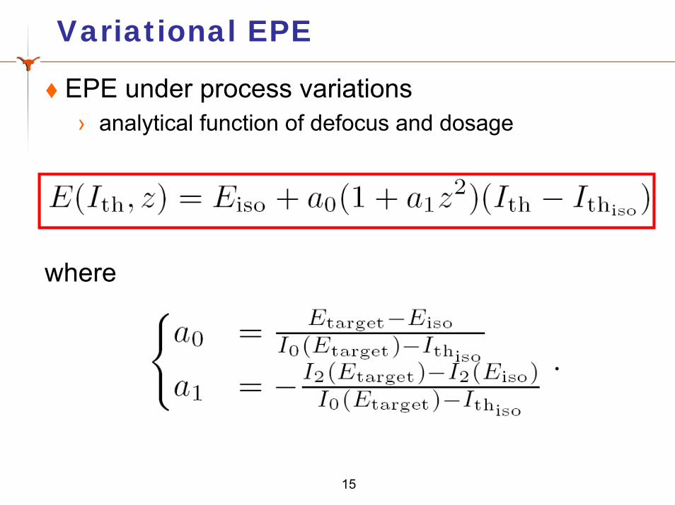
Variational EPE
EPE under process variations› analytical function of defocus and dosage
where

16
Given certain focus and dosage variations, e.g.
=> Analytical V-EPE metrics, e.g., first moment
Variational EPE Example
Concepts are generic to other “raw” distributions of focus/dosage or variational EPE metrics

17
Applications: PV-OPC and Beyond
Key Idea: Derive/Extract variational EPE from “raw” variations: focus and dosage, etc.Run time only 2-3x compared to nominal process, but explicitly consider process variationsCan be used to guide true PV aware OPC (PV-OPC) or litho-aware routing
[Yu et al, DAC’06]US Patent Pending (supported by SRC)

18
Geometry => Electrical
I-V curves with Vgs = 0.4, 0.8, 1.2V NMOS Leakage with Vds = 1.2V
Electrical characterizations of a 65nm inverterPV-OPC is able to meet design intent under process variations
3x difference in leakage!
PV-OPCIdeal mask
Conventional OPC

19
Variational Electrical Analysis
Layout-dependent non-rectangular gate characterization [Shi+, ICCAD’06]
=> more accurate static/statistical circuit analysisA novel sparse-matrix formulation for SSTA [Ramalingam+, ICCAD’06]
› Model path-based SSTA using sparse matrix multiplication (fast Monte-Carlo in one-short)
› Handle arbitrary correlations› Handle slope propagation › Very accurate and fast!› Can use block-based SSTA for path-pruning

20
Path Enumeration
½ adder example:a
b
c
d
e
f
g
a b c1 c2 d1 d2 e1 e2 f1 f2
1
1
1
1
1
1
g
1
1
1
1 1
1
1 1
All i/p – o/p, latch-latchpaths are represented
Each column is an input pin
Each row is a complete path
A 1 means input pin is on
this path
Incidence matrix is quite
sparse!
Path delays can be written in p = A d.

21
Delay Modeling
By linear regression, express gate delay as a polynomial in:
› Operating environment, e.g., CLoad
› Technology variables, e.g. L, VT
Linear regression (≠ Linear models), e.g.:› d = c0 + c1 CLoad L2 + c2 L VT
½ – …
Collect all regression terms into one vector z› d = cT z
Regression term z1 Regression term z2

22
Gate delay VectorDelay for gate k: dk = ck
T zk› dc1 denotes the delay from
gate c’s pin 1 to o/pExpanding for all gates/arcs:
da = caT za
db = cbT zb
dc1 = cc1T zc1
dc2 = cc2T zc2
dd1 = cd1T zd1
dd2 = cd2T zd2
…
=> d = C z
a
b
c
d
e
f
g

23
Path Delays using Monte-Carlo
Equation for all path delays given by:› p = A d = A C z
Values of z determined by technology settings such as VT, L, VDD etc.
› Given an arbitrary distribution of z, we can generate n samples Z = [z1 … zn]
Path delays corresponding to these n samples:› [p1 … pn] = A C [z1 … zn]
Fast Monte-Carlo SSTA in sparse-matrix form:› P = A C Z
Handle slope propagation nicely (a new C’ matrix)Method implemented/used by industry.

24
OutlineBackground & Motivation DFM Modeling, OPC and Characterizations
› Design-oriented, PV-aware lithography simulation› Variational characterization & electrical analysis
DFM Optimizations› DFM aware routing› Variation-tolerant design
Conclusions

25
Blockage
Routing in VLSI Physical Design
Global Routing
Track Routing
Detailed Routing
Placement
Routing
Manufacturing
Routing
a
a
a
a
b
bc
c
c
d
d

26
Yield Loss Mechanisms
[Courtesy IBS]
Critical Area
CMP
Lithography

27
Which Stage to Tackle What?
CMP variation optimization› Minimum effective window (20x20μm2) and global effect› Global routing plans approximate routing density
Critical area optimization › Adjacent parallel wires contribute majority of critical area.› Track router has good flexibility with wire ordering/spacing/sizing.
Lithography optimization› Effective windows (1-2μm2 ) are small › Detailed router performs localized connection between pins/wires.
Global Routing
Track Routing
Detailed Routing
CMP variation optimization
Critical area minimization
Lithography enhancement

28
Litho-Aware RoutingMore & more metal layers need RETsRule vs. model based approachRules -
› Exploding number of rules › Very complicated rules › Too conservative or not accurate rules› No smooth tradeoffs (either follow or break rules)
How about directly link litho-models with routing?› Lithography simulations could be extremely slow !› A full-chip OPC could take a week › Accuracy vs. Fidelity (Elmore-like)› Design-oriented vs. process-oriented

29
RET-Aware Detailed Routing (RADAR) [Mitra et al, DAC’05]
First work to truly link lithography modeling with design implementation levelIntroduce the concept of Litho- Hotspot Maps Fast lithography simulation to generate LHM
› Guided by our design-oriented fast litho simulationsPost-routing optimizations to reduce hotspots
› Wire spreading› Ripup-Reroute (RR) with blockages (protect “good”
regions)

30
RET-aware Routing on a 65nm Design
Initial routing (afterdesign closure)
40% EPE reduction(much less litho hot spots)
[Mitra et al, DAC’05]

31
More on Litho-Aware Routing
Lithography hotspot is a generic conceptOther metrics may be used: Not just EPE
› Possibly under process variations, such as variational EPE (V-EPE) metric [Yu+, DAC’06]
› Other Predictive OPC modeling [SPIE’07]We are developing a new correct-by-construction litho-aware router

32
CMP-Aware Routing
Lithography interact with CMP› CMP => defocus
CMP-Aware Routing› Need scalable yet high-fidelity CMP model› Best attacked at the global routing stage

33
Wire Density Driven Paradigm[Cho et al, ICCAD’06]
In general, more uniform wire density › Better CMP topography variations
Wire density will affect timing too› Lower wire density => less resistance (higher thickness)› Lower wire density => less capacitance
Wire density: a unified metric for CMP and Timing optimization (one stone, two birds!)Wire density vs. congestion driven GR
› Though correlated, indeed different during global routing› Density: wires inside global routing cells› Congestion: wires crossing the boundaries of global routing
cells

34
BoxRouter [DAC’06, ICCAD’07]
Incremental Box Expansion
› From most congested regions
Progressive ILPAdaptive maze routingPostRouting
› Negotiation-based approach
DAC’06 BPA Candidate2nd place (in 3D) ISPD07 Routing Contest US Patent filed by SRCOpen Source Released
Global routing cell (G-cell)

35
Predictive Copper CMP Model
Global Routing
Predictive
CMP Model
Wire Density
Cu Thickness
Verified by physics-based simulations

36
Predictive Copper CMP Model
Density vs Thickness
0.8
0.85
0.9
0.95
1
24%28%32%36%40%44%48%52%56%60%64%68%72%76%80%Metal Density
Nor
mal
ized
Thi
ckne
ss
Average Dummy Density Distribution (TILE=20um)
0%
10%
20%
30%
40%
0% 10% 20% 30% 40% 50% 60% 70% 80% 90% 100%Wire Density
Dum
my
Fill
Den
sity
Calculate Wire Density
Required Dummy Density(From Lookup Table)
Metal Density = Wire Density + Dummy Density
Thickness = A*(1- Metal Density2/B)
[Cho et al, ICCAD’06]

37
Global Routing Flow With Predictive CMP Model
Global Routing
Wire Density
Cu Thickness
Dummy Fill DensityFrom Lookup Table
Metal Density= Wire Density+
Dummy Fill Density
Cu Thickness
Predictive CMP Model for Global Routing
Predictive CMP Model guides global router› More uniform wire distribution› Consider metal blockages (power/ground rail, IPs)
BoxRouter

38
Experimental Results
0.840.860.880.9
0.920.940.960.98
1
Nor
mal
ized
Var
iatio
n
ibm01 ibm02 ibm03 ibm04 ibm05 ibm06 ibm07 ibm08 ibm09 ibm10
BoxRouter Wire density
On average 7.5% reductionUp to 10.1% reduction
0.840.860.880.9
0.920.940.960.98
1
Nor
mal
ized
tim
ing
ibm01 ibm03 ibm05 ibm07 ibm09
BoxRouter Wire density
CMP variation
On average 7% reductionUp to 10% reduction
Timing
[Cho et al, ICCAD’06]

39
Critical Area For Yield
Random defect can cause open/short defect› Wire planning for critical area reduction
Defect size distribution› Chance of getting larger defect decreases rapidly [TCAD85]
Concurrent optimization for open/short defect› Larger wire width for open, but larger spacing for short defect› Limited chip area
B
A
C Critical area due to open defect› Reduce defect size› Increase wire width
Critical area due to short defect› Reduce defect size› Increase wire spacing

40
Track Routing for Yield (TROY) [Cho et al, DAC’07]
TROY is the first yield-driven track router› Wire ordering to minimize overlapped wirelength
between neighbors» Preference-aware Minimum Hamiltonian Path
› Wire sizing/spacing to minimize critical areas» Second-order conic programming (SOCP)» global optimal in nearly linear time
Result is very promising› 18% reduction in yield loss due to random defects› TROY is very scalable

41
Math 101 for Critical Area
Defect size distribution r =3
Critical are due to open defect
Critical are due to short defect
Probability of failure (POF) for open/short defects
Approximated POF
POFs for open/shorts are convex functions› Global optimal can be found, but POF is complicated.› Approximated POF is also convex, but easy enough to enable SOCP.

42
TROY Brute-forth Formulation
Integer nonlinear programming› Extremely hard to solve› Integer variable for the wire order oij (above/below relationship)
POF for open
POF for short
Min/max width and spacing constraints,
and desired locations

43
TROY Strategy
Integer nonlinear programming
Wire ordering
Second order conic programming (SOCP)
Wire sizing/spacing
SOCP: Global optimal solution in nearly linear time
Solved by finding minimum Hamiltonian path

44
TROY Results
0200400600800
100012001400
Yiel
d lo
ss o
ut o
f 10K
ibm01 ibm02 ibm03 ibm04 ibm05 ibm06 ibm07 ibm08 ibm09 ibm10
TCAD01 TROY TROY.DGreedy algorithm [Tseng TCAD01]TROY: continuous wire width
[Cho et al, DAC’07]
Monte-Carlo simulation with 10K defectsOn average 18 % reduction in yield loss, up to 30%Discretization only loses 2%
TROY.D: discrete wire width

45
DFM-Aware Routing Wrap-up
The reality is of course, MORE COMPLICATEDNeed to consider the interactions between CMP, Litho, RV, CAA, etc.
Global Routing
Track Routing
Detailed Routing
CMP variation optimization
Critical area minimization
Lithography enhancement
Redundant via enhancement

46
Variation-Tolerant Clock SynthesisVariation reduction => variation toleranceTemperature aware clock opt. [ICCAD’05]Clock tree link insertion [Rajaram+, ISPD’05, ISQED’06, ISPD’06, ISQED’07]Meshworks: clock mesh planning/synthesis [ASPDAC 2008, BPA nominee]
Mesh -> remove links?CTS -> add links

47
Conclusions
193nm lithography will still be the dominant chip manufacturing workhorse, for next 5+ years
› Even EUV still has DFM problemsSynergistic modeling & optimization needed in a unified framework => Design + Mfg Closure
› DFM in context of DSMCurrent works just scratch the surfaceNeed much closer collaborations than ever
› Between academia and industry (e.g., SRC, IMPACT)› Between different camps: design, CAD, process, and
system!

48
Acknowledgment
Sponsorship by NSF, SRC (core + custom funding from AMD/Cadence/Freescale), IBM, Fujitsu, Qualcomm, Sun, Intel and KLA-TencorPhD students at UTDA: Minsik Cho, Joydeep Mitra, Anand Rajaram, Anand Ramalingam, Sean X. Shi, Peng YuCollaborations/discussions with Dr. Chris Mack, Dr. Ruchir Puri, Dr. Hua Xiang, Dr. Warren Grobman, Dr. Vassilios Gerousis, Dr. Riko Radojcic, et al.


![Guided drives DFM/DFM-B · Guided drives DFM/DFM-B Product range overview Function Version Type Piston Stroke Variable stroke [mm] [mm] [mm] Double-acting DFM basic version with recirculating](https://static.fdocuments.net/doc/165x107/60075e4355302d48df775d82/guided-drives-dfmdfm-b-guided-drives-dfmdfm-b-product-range-overview-function.jpg)