Synchroscalar: Evaluation of an Embedded, Multi-core Architecture
16
Synchroscalar: Evaluation of an Embedded, Multi-core Architecture for Media Applications John Oliver , Ravishankar Rao , Diana Franklin , Frederic T. Chong and Venkatesh Akella University of California, Davis University of California, Santa Barbara California Polytechnic State University, San Luis Obispo John Oliver: 2064 Kemper Hall Davis, CA 95616-5294 Tel: (530) 752-1417 Abstract We present an overview of the Synchroscalar single-chip, multi-core processor. Through the design of Synchroscalar,we find that high energy efficiency and low complexity can be attained through parallelization. The importance of adequate inter-core interconnect is also demonstrated. We discuss the impact of having multiple frequency and voltage domains on chip to reduce the power consumption where parallelization fails. Finally, we investigate how the ad-hoc selection of tile size that is currently used in most single-chip multi-core processors impacts the power consumption of these architectures. Keywords: Embedded Processing, Media Processing, Multicore Processor, Low-Power 1
Transcript of Synchroscalar: Evaluation of an Embedded, Multi-core Architecture

Synchroscalar: Evaluation of an Embedded, Multi-core Architecture for Media
Applications
John Oliver�
, Ravishankar Rao�
,
Diana Franklin�
, Frederic T. Chong�
and Venkatesh Akella�
University of California, Davis�
University of California, Santa Barbara�
California Polytechnic State University, San Luis Obispo�
John Oliver: 2064 Kemper Hall
Davis, CA 95616-5294
Tel: (530) 752-1417
Abstract
We present an overview of the Synchroscalar single-chip, multi-core processor. Through the design of Synchroscalar, we
find that high energy efficiency and low complexity can be attained through parallelization. The importance of adequate
inter-core interconnect is also demonstrated. We discuss the impact of having multiple frequency and voltage domains on
chip to reduce the power consumption where parallelization fails. Finally, we investigate how the ad-hoc selection of tile size
that is currently used in most single-chip multi-core processors impacts the power consumption of these architectures.
Keywords: Embedded Processing, Media Processing, Multicore Processor, Low-Power
1
1 Introduction
In this article, we present some design-space lessons learned from the refinements of the design of the Synchroscalar archi-
tecture. Synchroscalar is a single-chip, multiple core low-power computer architecture which is intended to support media
applications. In particular, there are four architectural features that impact the power consumption of single-chip, multi-core
architectures that we investigate using the Synchroscalar architecture as a basis. First, we exhibit the amount of power that can
be saved by utilizing an appropriate amount of computational parallelism for a given application. Next, the power consump-
tion impact of inter-core interconnect is demonstrated. Thirdly, we look at how voltage scaling can be used to cost-effectively
reduce the power consumption of multi-core architectures. Finally, we demonstrate that through the careful selection of the
amount of computational parallelism within a tile, we find we can reduce the power consumption of the architecture.
The rest of this article is structured as follows. First, we will begin with a brief description of the Synchroscalar architec-
ture. Next, we will talk about the algorithms and applications used to test this architecture’s performance and the methodology
used to find power results for Synchroscalar. We will then see the power consumption of the Synchroscalar architecture of a
few end-to-end applications and discuss how our four few key design features impact power consumption. Finally, we will
finish up with some directions for future work and conclude.
2 The Synchroscalar Architecture
The high-level observation that led to the Synchroscalar design was that if an application can be efficiently mapped on a
multi-core architecture, then the clock and voltage can be scaled down on each core in order to reduce power consumption.
Synchroscalar tiles are based upon the Blackfin [16] Digital Signal Processor, which can be thought of as 2-way VLIW
processor. These tiles are organized in columns, where each column consists of four Blackfin-like tiles running in SIMD
mode and at a statically programmable voltage and frequency. The column nature of Synchroscalar allows us to greatly reduce
the complexity of control, communication, clock distribution and voltage domains. Each column has a SIMD controller that
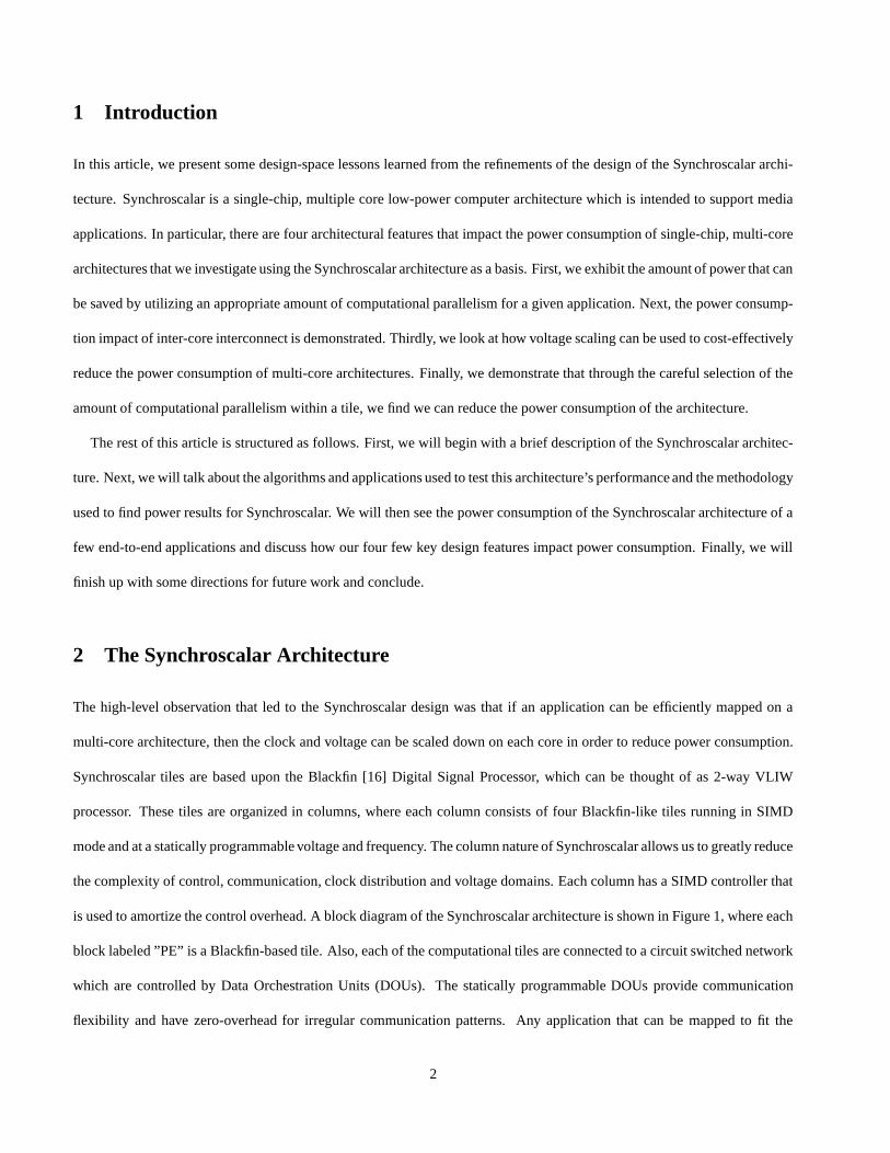
is used to amortize the control overhead. A block diagram of the Synchroscalar architecture is shown in Figure 1, where each
block labeled ”PE” is a Blackfin-based tile. Also, each of the computational tiles are connected to a circuit switched network
which are controlled by Data Orchestration Units (DOUs). The statically programmable DOUs provide communication
flexibility and have zero-overhead for irregular communication patterns. Any application that can be mapped to fit the
2
Synchronous Dataflow (SDF) model of computation can be supported by the Synchroscalar architecture. SDF models of
computation have been supported in many other implementations [8, 9, 10]. The rest of this section gives a brief overview of
the Synchroscalar architecture. More specifics on the Synchroscalar architecture can be found in [21].
Parallelism is critical to the low-power operation of Synchroscalar, for it is through parallelism that we can reduce
the clock frequency, and thus voltage, while continuing to meet performance targets. In this we are greatly aided by the
statically-predictable, highly data-parallel nature of signal processing. For this study, our applications are all iteratively
hand-parallelized until the lowest power consumption for a given application is attained.
Inter-tile Interconnect is critical to the performance of multi-core processors. Like other multi-core processors, Syn-
chroscalar exploits parallelism to increase efficiency rather than performance. However, these gains must not be lost to the
communication overhead. Latency-critical communication must not be allowed to increase the idle time of power-hungry
processor tiles, especially when idle times are too small to shut down tiles. Therefore, we invested considerable area to
inter-tile interconnect on the Synchroscalar architecture.
Synchroscalar buses are 256 bits wide, grouped into 8 32-bit separable vertical buses that are segmented in between each
of the tiles. Given our design goal of low system clock rates, we find that we can approximate the specialized interconnects of
ASICs through a combination of segmented buses and a decoupled communication controller called the Data Orchestration
Unit (DOU). Refer back to Figure 1 to see these buses and the DOUs (both marked in gray) arranged in each column.
By suitably configuring the segment controllers, the bus can perform several parallel communications. For instance, if
all the controllers are turned on, the bus becomes a low-latency broadcast bus, and all tiles able to receive the same data in
a single cycle. Alternatively, two messages can pass between neighboring tiles using the same wires in different segments,
achieving the bandwidth of a mesh.
The DOU provides zero-overhead data movement between producer and consumer tiles. A producer writes to a special
register and at a deterministic statically-scheduled time a consumer can read that value from a receive register. The DOUs
provide separate, cycle-by-cycle control of data motion and interconnect configuration. This flexibility facilitates irregular
data motion and allows our applications to be efficiently scheduled in SIMD tile computations. More details about the
operation of the DOU can be found in [21].
A centralized SIMD Controller performs all control instructions for each column of tiles, only forwarding computation
instructions to the individual tiles. To communicate data for conditional branches, the SIMD controller is connected to the
3
segmented bus with the tiles. Utilizing a SIMD controller makes sense for the data-parallel nature of signal processing
applications as it allows a reduction in the cost of instruction fetch and decode.
Clock and voltage Domains can be configured for each column of tiles so that the tiles operate at the lowest frequency
that meets the application constraints and the corresponding voltage. A voltage and frequency floor of 0.7 V and 100 MHz is
ensured for reliability.
3 Methodology
We now present an overview of the evaluation framework for Synchroscalar as presented in [21]. Due to space constraints,
we only include a few of the highlights of the Synchroscalar design in this paper. The design of Synchroscalar included the
an application mapping methodology, tile and interconnect power models, VHDL synthesis, and cycle-accurate simulation.
Implementing Applications on Synchroscalar
The following is an enumeration of the steps needed to efficiently map an application to Synchroscalar:1. Start with the description of the application on a single tile (typically C or Blackfin assembly).2. Partition the application into N tiles and insert data transfer operations to model the inter-tile communications.3. Assume every data transfer takes one clock cycle. Statically schedule all the data transfers.4. NOPS are introduced appropriately to avoid structural hazards due to bus conflicts.5. Use the cycle-accurate simulator to determine the number of clock cycles required per input data sample. Code and data
are in local tile memories when computing the clock cycle count.6. Given the input data rate and number of cycles required by each tile compute the operation frequency and voltage required.7. Compute the total power using the Synchroscalar power model8. Reiterate with a new N, until the lowest power is attained.
Tile Model
The power consumption of our Blackfin-based tile was estimated by using a combination of published power results for
micro-architectural structures and VHDL synthesized using the Synopsys Design compiler in 130nm process technology.
See [21] for full details of the power estimation of our tiles. Through this estimate, we find that the Blackfin-based tiles
operate at 0.1 mW/MHz at a 1V supply, which is reasonable since a similar core from NEC, the SPXK5 [25], consumes
0.07mW/MHz. The area estimate of the Blackfin core is 1.82 ����.
Interconnect Model
The interconnect model is largely based on the data from ”The Future of Wires” paper [14]. The projected value of wire
capacitance for a semi-global wire in 0.13 � technology is per unit length is 387fF/mm. Assuming length of the chip is
4

about 10mm (that corresponds to the length of the bus) the wire capacitance is about 3870fF. If the bus drivers and repeaters
are 10-times the minimum size, their capacitance contribution is about 20fF. If there are 8 drivers for each bus, it adds only
160fF to the wire capacitance which is much smaller than the wire capacitance. Thus the interconnect is modeled by the wire
capacitance to a first order approximation. The cycle delay of the interconnect model is simulated by a custom interconnect
simulator.
Leakage Power Estimation
We calculate the leakage current, ������� as 830 pA per transistor for a minimum sized transistor. This leakage correlates well
with the number published by Intel on their 130 nm process where leakage current varies from 0.65 nA per transistor to 32.5
nA per transistor depending if the threshold voltage of the transistor [31]. We estimate 1.8 million transistors per tile, so we
assume that the leakage power to be around 1.5 mA per tile assuming 830 pA of leakage per transistor.
Cycle-Accurate Simulation
To obtain cycle-accurate performance measurements, we adapted an object-oriented variant of SimpleScalar [11] to model
the Synchroscalar architecture. The instruction set was re-targeted to the Blackfin ISA [16] and communication mechanisms
were added. This simulator was validated against the cycle-accurate Blackfin Simulator called VisualDSP over several key
DSP assembly kernels, such as FFT, FIR filters and IIR filters. The applications were compiled, and the inner-loops were
hand-optimized in Blackfin assembly. Inter-tile communication were hand-scheduled, and nops were inserted as specified by
our interconnect simulations.
Applications
To drive the design of Synchroscalar, we selected four signal-processing applications, each of considerable complexity in-
volving several computational subcomponents. Digital Down Conversion (DDC) is an integral component of many software
radios and communication systems. This particular DDC was configured to support GSM cellular requirements of up to
64M samples per second. Stereo Vision (SV), was used in the Mars Rover[18]. Each frame processed is 256 by 256 pixels
in monochrome and is processed at a rate of 10 frames per second. An 802.11a receiver is an IEEE standard for wireless
communications and supports data rates up to 54 Mbps. The dominant computations within 802.11a are an inverse FFT, FIR
filter and Viterbi error correction. Finally, MPEG-4 is a compression application and was implemented for both CIF and
QCIF at 30 frames per second.
5

4 Results and Discussion
Since all of our applications have set performance targets, our metric is the system power required to achieve those targets.
Table 1 summarizes the primary success of Synchroscalar: software implementation of challenging signal processing ap-
plications with energy efficiency generally within 8-30X of ASIC solutions and 10-60X better than DSPs performing even
reduced data rate versions of the applications.
The remainder of this section has four subsections. First we look at architectural features of Synchroscalar that were
successful in reducing overall system power, namely the ability to apply parallelism to computationally intensive tasks. Then
the impact of inter-tile interconnect on power consumption will be discussed. Next, we look at how distinct voltage domains
improve power consumption and how the impact of voltage domains may be improved. Finally, we will re-investigate the
design choice of using Blackfin-based tiles as the elemental tile of the Synchroscalar computational array.
4.1 Impact of Parallelism
Because we can statically allocate the amount of parallelism that is efficient for the execution of an application, parallelism
becomes the main weapon in the Synchroscalar arsenal to reduce power consumption. However, parallelism is not without
it’s cost.
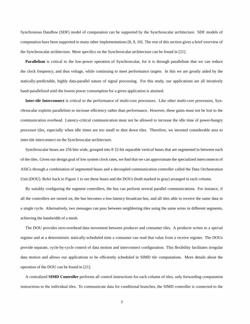
Figure 2 shows how much power is consumed for different levels of parallelization of the our applications on the Syn-
chroscalar architecture. From Figure 2, we can clearly see that having ample parallelism is one method of attaining low-power
operation. The MPEG-4 application is a good example of how parallelism can be used to reduce the system power. By allo-
cating more parallel resources we are able to run the applications at a lower frequency and a lower voltage, thereby saving
power.
However, there are diminishing returns for further parallelization in terms of increased inter-tile communications and
leakage current. In the 802.11a parallel implementations shown in Figure 2 the communications overhead negatively impacts
our power efficiency and is represented by the black portions of the bars. Another source of diminishing returns from further
parallelization is a supply voltage floor. By parallelizing an algorithm that is already running at the minimum supply voltage,
we would not yield further power savings. Finally, we should note that area constraints (limited numbers of Synchroscalar
tiles) also may limit the amount of parallelism that can be efficiently allocated.
6

4.2 Impact of Interconnect
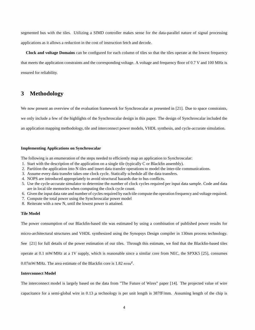
In Figure 3 we have mapped how the power-area efficiency of the Synchroscalar architecture scales for the Viterbi Add-
Compare-Select (ACS) with different sets of bus widths and different numbers of tiles. The Viterbi ACS is used here as
the Viterbi decoder has the most demanding communications requirements of any of the individual algorithms tested on the
Synchroscalar architecture. The three curves on Figure 3 each represent a Viterbi ACS trellis being completed on 8, 16
and 32 tiles. Each of the curves are comprised of power results for a few different bus widths (32b, 64b, 128b, etc...). We
can see from this figure that increasing the bus width from 128 to 256 bits significantly improves the power efficiency of
Synchroscalar on the Viterbi Decoder for all three implementations. The lesson here is that investing in inter-tile interconnect
can help reduce power consumption greatly, but it comes at the cost of added area. Nevertheless, a multi-core processor that
is constrained by the inter-tile interconnect will not efficiently consume power.
4.3 Impact of Voltage Domains
The Synchroscalar architecture has the ability to support multiple frequency and voltage domains on a per-column basis.
These frequency and voltage domains are configurable at start-up. Different portions of applications can be mapped to
different processors, and the frequency of these processors can be fine-tuned to each portion’s needs. By reducing the
frequency of the tiles to their required rates, we can also reduce the voltage of those tiles as well. Thus, allowing for multiple
voltage domains saves the Synchroscalar architecture power.
Figure 4 shows the power consumption of four applications. The total height each bar is the power consumed if the
Synchroscalar architecture did not support different voltage domains while the height of only the white portion of each bar is
the power consumption for Synchroscalar with multiple voltage domains. From this figure we find that the impact of having
different voltage domains is significant in some cases, such as Stereo Vision and Digital Down Conversion.
As signal chains get longer, like when AES (a encryption/decryption algorithm) is added to the 802.11a signal chain, we
find that having multiple voltage domains is more important.
In many highly-parallel media codes, we acknowledge that it is possible to reduce the power consumption by using more
tiles because this brings down the frequency and therefore the voltage of the entire chip. However, more tiles means more
area whereas having multiple voltage domains would be a more area-sensitive manner in which to reduce system power.
Therefore, support of multiple voltage domains is a lighter-weight method of reducing overall power consumption. This is
7

demonstrated in Figure 5 where we see significant power reduction for some of our applications without significant area
growth simply by supporting multiple voltage domains.
Also, applications that have a high data rate portion which cannot be easily or efficiently parallelized benefit the most from
having multiple voltage domains. This can be seen in the SV application in Figure 5. The black squares represent SV at three
different levels of parallelization with multiple voltage domains enabled, while the white squares (the white square at 27.81
����
overlaps with middle black square at 27.81 � ��) represent SV at the same parallelization levels without multiple
voltage domains. We can see without voltage scaling, further parallelization from 27.81 � ��
to 52.53 � ��
yields only
about a 4% reduction in power, while with multiple voltage domains, we can get a 35% reduction in power. Thus, having
multiple voltage domains in some cases may enable us to utilize additional parallelism to further reduce system power.
Future work includes studying the impact of having multiple voltage domains on a multi-core processor where the cores
have more computational power. Since cores with more computational power are typically larger, we suspect voltage scaling
will play a more important role here as well.
4.4 Optimizing Tile Compute Width
Choosing a tile size for many single chip multiprocessors has typically been an ad-hoc, qualitative process. Indeed, in the
design of Synchroscalar, we chose to use the Blackfin DSP because of the performance and power consumption properties of
this DSP core, making the assumption that efficient tiles make for an efficient multi-core architecture. However, we find that
cores with more computational power which use more energy per operation improves the power consumption of a range of
signal processing benchmarks.
We define larger tiles to have more computational parallelism than smaller tiles, but larger cores are also more highly
interconnected within the tile than a smaller tile. Thus the average switching capacitance per computation of a larger tile
higher is than a smaller tile. However, there is a trade-off. An array of many small cores will expose more data-movement
to an inter-tile interconnect network, and thus have higher latency for data sharing. This latency, for fixed-rate applications,
translates into higher operational frequencies which impacts power consumption.
In order to investigate this trade-off on a multi-core processor, we first need a tile model with different computational
widths and therefore power consumptions. In this section, we will hold the aggregate amount of computational parallelism
constant to 32 parallel computations in any given cycle. We will only be changing the distribution or granularity of the
8
computational parallelism. Thus, we could have a single large core with a computational width of 32, or use 32 single-width
cores. Then, we partition and map algorithms onto these different sized cores. Finally, we run simulations to find the perfor-
mance of these algorithms on arrays with different granularities need to be performed.
Processor Tile Model
We define the computational width of a tile as the maximum number of arithmetic operations that can be completed per
clock cycle, where the operands are in the local register file. The smallest tile we consider in this study can compute a single
operation in every cycle, while the largest tile we consider can compute 32 operations in parallel every cycle. We assume a
VLIW-based architecture, similar to the Blackfin DSP which has a computational width of two.
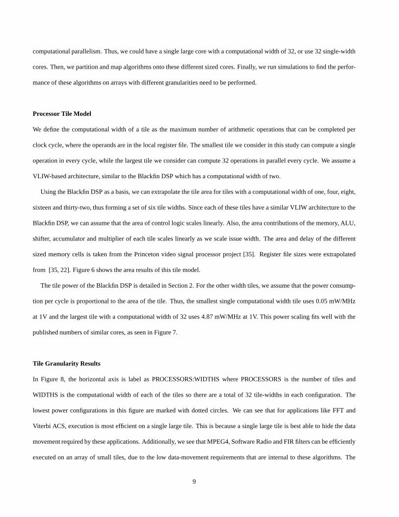
Using the Blackfin DSP as a basis, we can extrapolate the tile area for tiles with a computational width of one, four, eight,
sixteen and thirty-two, thus forming a set of six tile widths. Since each of these tiles have a similar VLIW architecture to the
Blackfin DSP, we can assume that the area of control logic scales linearly. Also, the area contributions of the memory, ALU,
shifter, accumulator and multiplier of each tile scales linearly as we scale issue width. The area and delay of the different
sized memory cells is taken from the Princeton video signal processor project [35]. Register file sizes were extrapolated
from [35, 22]. Figure 6 shows the area results of this tile model.
The tile power of the Blackfin DSP is detailed in Section 2. For the other width tiles, we assume that the power consump-
tion per cycle is proportional to the area of the tile. Thus, the smallest single computational width tile uses 0.05 mW/MHz
at 1V and the largest tile with a computational width of 32 uses 4.87 mW/MHz at 1V. This power scaling fits well with the
published numbers of similar cores, as seen in Figure 7.
Tile Granularity Results
In Figure 8, the horizontal axis is label as PROCESSORS:WIDTHS where PROCESSORS is the number of tiles and
WIDTHS is the computational width of each of the tiles so there are a total of 32 tile-widths in each configuration. The
lowest power configurations in this figure are marked with dotted circles. We can see that for applications like FFT and
Viterbi ACS, execution is most efficient on a single large tile. This is because a single large tile is best able to hide the data
movement required by these applications. Additionally, we see that MPEG4, Software Radio and FIR filters can be efficiently
executed on an array of small tiles, due to the low data-movement requirements that are internal to these algorithms. The
9

802.11a application, which consists of FFT, FIR, Viterbi ACS and Viterbi traceback (a mix of algorithms with high and low
data movement requirements), shows the best power consumption with two tiles each with a computational width of 16.
From Figure 8, we can clearly see that the optimal granularity of tile depends upon the data-movement requirements
internal to the algorithm. We also see that the impact of choosing the incorrect granularity of tile can be large. In fact, the
power differential between worst-case and best-case granularity of tiles for the Software Radio application can be as large as
four times!
In many ways, Synchroscalar was designed to efficiently support the 802.11a application. As we can see from Figure 8,
choosing tiles with a computation width of two was a sub-optimal choice. In the next revision of the Synchroscalar design,
larger tile sizes will be considered and weighed against the area cost of larger tiles. Another possible future direction includes
finding the best granularity for a set of embedded benchmarks, such as EEMBC or MediaBench.
5 Related Work
Two primary influences on the design of Synchroscalar are MIT’s Raw architecture [26] and the Stanford’s Imagine Proces-
sor [23]. While all single chip, multi-core architectures share a few commonalities, Synchroscalar has a few features that sets
it apart from both the Raw and Imagine architectures. First, low-power operation is the focus of the Synchroscalar processor,
not performance. Additionally, the frequency and voltage domains of Synchroscalar differentiate Synchroscalar from Raw
and Imagine. Finally, Synchroscalar exploits static data flow through the use of Data Orchestration Units to reduce power
consumption.
6 Conclusion
The design principles of Synchroscalar – high parallelism, efficient interconnect, low control overhead, and custom frequency
domains – will lead to a new set of embedded architectures with efficiency approaching ASICs and with the programmability
of DSPs. We find that supporting multiple voltage domains on chip can be a lighter weight method of reducing system power
rather than simply using parallelism alone. Adequate inter-tile interconnect is critical to low-power operation. Finally, we
find that the power consumption of embedded multi-processor chips is greatly impacted by not only the total amount of
parallelism available, but the distribution of this parallelism as well.
10
References
[1] Amphion. Amphion CS6701 Hybrid MPEG-4 Video Encoder. http://www.amphion.com/cs6701.html.
[2] Analog Devices Press Release: Blackfin. http://www. electronicstalk.com/ news/anc/anc199.html, March 2003.
[3] ADSP-2191 Processor Data Sheet. 2002.
[4] TS-101 Data Sheet. August 2002.
[5] H. Arakida, M. Takahashi, Y. T. 1, T. Nishikawa, , H. Yamamoto, T. Fujiyoshi, Y. Kitasho, Y. Ueda, M. Watanabe, T. Fujita, T. Terazawa, K. Ohmori,
M. Koana, H. Nakamura, E. Watanabe, H. Ando, T. Aikawa, and T. Furuyama. A 160mW, 80nA standby, MPEG-4 audiovisual LSI with 160mb
embedded DRAM and a 50GOPS adaptive post filter. In International Solid-State Circuits Conference, Digest of Technical Papers, Feb. 2003.
[6] B. M. Baas. A parallel programmable energy-efficient architecture for computationally intensive DSP systems. In Conference Record of the Thirty-
Seventh Asilomar Conference on Signals, Systems, and Computers, nov 2003.
[7] A. Benedetti. Personal communication, 2003.
[8] S. Bhattacharya, P. Murthy, and E. Lee. Software synthesis from dataflow graphs, 1996.
[9] S. Bhattacharya, P. Murthy, and E. Lee. Synthesis of embedded software from synchronous dataflow specifications. Journal of VLSI Signal Processing,
(21):151–166, June 1999.
[10] J. Buck et al. Ptolemy: A framework for simulating and prototyping heterogenous systems. Int. Journal in Computer Simulation, 4(2), 1994.
[11] D. C. Burger and T. M. Austin. The simplescalar tool set, version 2.0. Technical Report CS-TR-1997-1342, University of Wisconsin, Madison, June
1997.
[12] David Su and Masoud Zargari and Patrick Yue and Shahriar Rabii and David Weber and Brian Kaczynski and Srenik Mehta and Kalwant Singh and
Sunetra Mendis and Bruce Wooley. A 5ghz cmos transceiver for ieee 802.11a wireless lan. In International Solid State Circuits Conference, 2002.
[13] S. A. et. al. A 600MHz VLIW DSP. February 2002.
[14] R. Ho, K. Mai, and M. Horowitz. The future of wires. In Proceedings of the IEEE, volume 89, pages 490–504, April 2001.
[15] Intel xeon processor 2.8 ghz datasheet. http://www. intel.com/design/xeon/datashts/298642.htm, March 2003.
[16] R. Kolagotla, J. Fridman, B. Aldrich, M. Hoffman, W. Anderson, M. Allen, D. Witt, R. Dunton, and L. Booth. High Performance Dual-MAC DSP
Architecture. IEEE Signal Processing Magazine, July 2002.
[17] R. P. Llopis, R. Sethuraman, C. A. P. H. Peters, S.Maul, and M. Oosterhuis. A low-cost and low-power multi-standard video encoder. In First
IEEE/ACM/IFIP International Conference on Hardware/Software Codesign and System Synthesis, 2003.
[18] L. Matthies, B. Chen, and J. Petrescu. Stereo vision, residual image processing and mars rover localization, 1997.
[19] H. Mizuno, N. Irie, K. Uchiyama, Y. Yanagisawa, S. Yoshioka, I. Kawasaki, and T. Hattori. SH-Mobile3: Application Processor for 3G Cellular
Phones on a Low-Power SoC Design Platform. Hot Chips 16, August 2004.
[20] E. Norden, P. Leteinturier, J. Barrenscheen, K. Scheibert, and F. Hellwig. A Fast Powertrain Microcontroller. August 2004.
11

[21] J. Oliver, R. Rao, P. Sultatna, J. Crandall, E. Czernikowski, L. W. Jones, D. Franklin, V. Akella, and F. T. Chong. Synchroscalar: A multiple clock
domain, power-aware, tile-based embedded processor. In 31th Annual International Symposium on Computer Architecture (31th ISCA-2004) Computer
Architecture News. ACM SIGARCH / IEEE, June 2004. http://www.ece.ucdavis.edu/ jyoliver.
[22] S. Rixner, W. Dally, B. Khailany, P. Mattson, U. Kapasi, and J. Owens. Register Organization for Media Processing. In International Symposium on
High Performance Computer Architecture (HPCA), Toulouse, France, January 2000.
[23] S. Rixner, W. J. Dally, U. J. Kapasi, B. Khailany, A. Lopez-Lagunas, P. R. Mattson, and J. D. Owens. A bandwidth-efficient architecture for media
processing. In International Symposium on Microarchitecture, pages 3–13, 1998.
[24] P. Ryan, T. Arivoli, L. de Souza, G. Foyster, R. Keaney, T. McDermott, A. Moini, S. Al-Sarawi, J. O’Sullivan, U. Parker, G. Smith, N. Weste, , and
G. Zyner. A single chip PHY COFDM modem for IEEE 802.11a with integrated ADCs and DACs. In International Solid State Circuits Conference,
2002.
[25] M. Y. T. Kumura, M. Ikekawa and I. Kuroda. VLIW DSP for Mobile Applications. IEEE Signal Processing Magazine, July 2002.
[26] M. B. Taylor, W. Lee, J. Miller, D. Wentzlaff, I. Bratt, B. Greenwald, H. Hoffmann, P. Johnson, J. Kim, J. Psota, A. Saraf, N. Shnidman, V. Strumpen,
M. Frank, S. P. Amarasinghe, and A. Agarwal. Evaluation of the raw microprocessor: An exposed-wire-delay architecture for ilp and streams. In
ISCA, pages 2–13, 2004.
[27] Texas Instruments GC4014 quad receiver chip datasheet. http://www-s.ti.com/sc/psheets/ slws132/slws132.pdf, April 1999.
[28] TMS320C28x Processor Manual. July 2001.
[29] TMS320C62x Processor Manual. July 2001.
[30] TMS320DM642 Data Sheet. 2005.
[31] S. Thompson, M. Alavi, M. Hussein, P. Jacob, C. Kenyon, P. Moon, M. Prince, S. Sivakumar, S. Tyagi, and M. Bohr. 130nm logic technology featuring
60nm transistors, low-k dielectrics, and cu interconnects. Intel Technology Journal, 6(2):5–13, May 2002.
[32] Transmeta Crusoe TM5700/5900 Processors. 2003.
[33] Transmeta Crusoe TM8300/8600 Processors. 2004.
[34] W. Eberle and V. Derudder and L. Van der Perre and G. Vanwijnsberghe and M. Vergara and L. Deneire and B. Gyselinckx and M. Engels and I.
Bolsens and and H. De Man. A digital 72Mb/s 64-QAM OFDM transceiver for 5GHz wireless LAN in 0.18um CMOS. In International Solid State
Circuits Conference, 2002.
[35] A. Wolfe, J. Fritts, S. Dutta, and E. S. T. Fernandes. Datapath design for a vliw video signal processor. In HPCA, pages 24–, 1997.
12

DOU
Clock Divider0
Clock Divider1
Clock Divider2
Clock Divider3
DOU DOU
PE
PE
PE
PE
PE
PE
PE
PE
PE
PE
PE
PE
PE
PE
PE
PE
I N D
A T
A
O U
T D
A T
A
PLL
SIMD Controller
SIMD Controller
SIMD Controller
SIMD Controller
Figure 1. The Synchroscalar Architecture
0
1
2
3
4
5
6
DDC 14 T
iles
DDC 26 T
iles
DDC 50 T
iles
SV 5 Tile
s
SV 9 Tile
s
SV 17 T
iles
802.1
1a 12
Tile
s
802.1
1a 20
Tile
s
802.1
1a 36
Tile
s
MPEG4 8 T
iles
MPEG4 12 T
iles
MPEG4 20 T
iles
MPEG4 36 T
iles
Po
wer
(W)
Interconnect + Leakage
Compute Power
Figure 2. Power Consumption of Applications with varying parallelization
0
1
2
3
4
5
6
7
8
9
10
0 20 40 60 80 100 120 140 160
Area (mm2)
Pow
er (
W)
32 Tiles 16 Tiles 8 Tiles
1024512
256
128
64
64
32
Figure 3. Power Consumption of Viterbi ACS with varying bus widths and parallelization
13

0.0
500.0
1000.0
1500.0
2000.0
2500.0
3000.0
3500.0
4000.0
4500.0
5000.0
DDC SV 80211.a MPEG4 -CIF
MPEG4 -QCIF
80211.a+ AES
Pow
er(m
W)
AdditionalPower w/ NoVoltage Scaling
Power, VoltageScaling
Figure 4. The Impact of Voltage Scaling on Power Consumption.
Figure 5. Area-Power Scatter Chart for Applications with and without Voltage Domains.
14
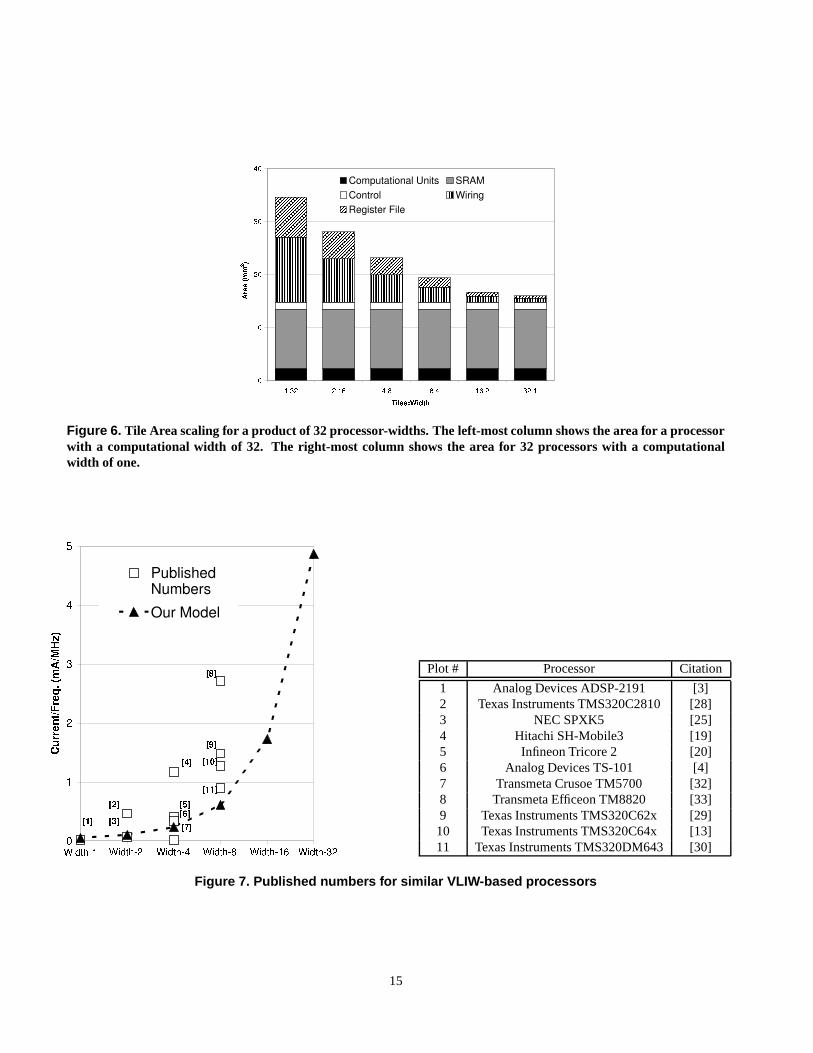
Figure 6. Tile Area scaling for a product of 32 processor-widths. The left-most column shows the area for a processorwith a computational width of 32. The right-most column shows the area for 32 processors with a computationalwidth of one.
Plot # Processor Citation
1 Analog Devices ADSP-2191 [3]2 Texas Instruments TMS320C2810 [28]3 NEC SPXK5 [25]4 Hitachi SH-Mobile3 [19]5 Infineon Tricore 2 [20]6 Analog Devices TS-101 [4]7 Transmeta Crusoe TM5700 [32]8 Transmeta Efficeon TM8820 [33]9 Texas Instruments TMS320C62x [29]
10 Texas Instruments TMS320C64x [13]11 Texas Instruments TMS320DM643 [30]
Figure 7. Published numbers for similar VLIW-based processors
15

Figure 8. Power Consumption of different algorithms for different tile granularities.
Process Area Power VoltageApp. Platform ( � )m ���
�(mW) (V) Notes
DDC Synchroscalar (50 Tiles) 0.13 139.88 2427.23 .7-1.3 Programmable, 64 MS/sIntel Xeon 2.8 GHz [15] 0.13 146 71000 1.45 Programmable, 19.0 MS/s, 1/3 req. rateBlackfin 600 MHz [2] 0.13 2.5 280 1.2 Programmable, 112.6 kS/s, 1/500 req. rateGraychip [27] UNK UNK 250 3.3V ASIC, 64 MS/s
Stereo Synchroscalar (17 Tiles) 0.13 52.89 857.40 1.2-1.5 Programmable, 10 f/s 256x256, stereoVision Intel Xeon 2.8 GHz [15] 0.13 146 71000 1.45 4.96 f/s, 1/3 required rate
Blackfin 600 MHz [2] 0.13 2.5 280 1.2 Programmable, 1.46 f/s, 1/7 required rateFPGA [7] UNK UNK 15K-25K UNK 30f/s 320x240,not stereo,no SVD, 1.75x rate
802.11a Synchroscalar (20 Tiles) 0.13 74.05 3930.53 0.7-1.7 Programmable, 54 Mbps RX onlyAtheros [6] 0.25 34.68 203 2.5 ASICIcefyre [24] 0.18 UNK 720 UNK ASIC Chipset, including ADCIMEC [34] 0.18 20.8 146 1.8 ASIC, area includes ADC/DACNEC [25] 0.18 119 474 1.5 ASIC, MAC+PHY layer, Core Power onlyD. Su [12] 0.25 22 121.5 2.7 PHY Layer onlyBlackfin 600 MHz [2] 0.13 UNK 280 1.2 Programmable, only 556 Kbps
MPEG4 Synchroscalar (10 Tiles) 0.13 32.32 47.24 0.7 QCIF @ 30 f/sQCIF Amphion [1] 0.18 110k gates 15 UNK Application-Specific Core, QCIF @ 15 f/s
Philips [17] 0.18 20 30 1.8 ASIP, QCIF @ 15 f/sBlackfin 600 MHz [2] 0.13 2.5 280 1.2 Programmable, QCIF @ 15f/s
MPEG4 Synchroscalar (16 Tiles) 0.13 31.74 370.03 1.1, 0.7 CIF @ 30 f/sCIF Toshiba [5] 0.13 43 160 1.5 SOC, CIF @ 15 f/s
Table 1. Power Comparison of Synchroscalar with other platforms.
16