Syllabus - · PDF filep-n junction diode, Characteristics and Parameters, ... Unit-IV: OTHER...
182
Basic Electronics 10ELN15 Dept. of ECE, SJBIT Page 1 Syllabus PART – A Unit I: SEMICONDUCTOR DIODES AND APPLICATIONS: 07 Hours p-n junction diode, Characteristics and Parameters, Diode approximations, DC load line, Temperature dependence of p-n characteristics, AC equivalent circuits, Zener diodes Half-wave diode rectifier, Ripple factor, Full-wave diode rectifier, Other full-wave circuits, Shunt capacitor - Approximate analysis of capacitor filters, Power supply performance, Zener diode voltage regulators, Numerical examples as applicable (T1-2.1,2.2,2.3,2.4:2.5,2.6,2.9,R1- 20.1, 20.2, 20.3, 20.4, 20.8; T1- 3.5, 3.6). Recommended readings: (T1) Electronic Devices and Circuits: David. A. Bell; PHI, New Delhi, 2004 Unit II: TRANSISTORS 06 Hours Bipolar Junction transistor, Transistor Voltages and currents, amplification, Common Base, Common Emitter and Common Collector Characteristics, DC Load line and Bias Point Unit-III: BIASING METHODS 06 Hours Base Bias, Collector to Base Bias, Voltage divider Bias, Comparison of basic bias circuits, Bias circuit design, Thermal Stability of Bias Circuits (Qualitative discussions only). (For Units II & III: T1- 4.1,4.2,4.3,4.4,4.5,4.6,5.1,5.2,5.3,5.4,5.5,5.7,5.9). Recommended readings: (T1) Electronic Devices and Circuits: David. A. Bell; PHI, New Delhi, 2004 Unit-IV: OTHER DEVICES 07 Hours Silicon Controlled Rectifier (S.C.R), SCR Control Circuits, More S.C.R applications; Uni-junction transistor, UJT applications, Junction Field effect Transistors(Exclude Fabrication and Packaging), JFET Characteristics, FET Amplifications, Numerical examples as applicable (T1 -19.1, 19.2, 19.3, 19.7, 9.1, 9.2, 9.4) Recommended readings: (T1) Electronic Devices and Circuits: David. A. Bell; PHI, New Delhi, 2004 Unit-V: AMPLIFIERS & OSCILLATORS 06 Hours Decibels and Half power points, Single Stage CE Amplifier and Capacitor coupled two stage CE amplifier(Qualitative discussions only), Series voltage negative feedback and Additional effects of
Transcript of Syllabus - · PDF filep-n junction diode, Characteristics and Parameters, ... Unit-IV: OTHER...
Basic Electronics 10ELN15
Dept. of ECE, SJBIT Page 1
Syllabus
PART – A
Unit I: SEMICONDUCTOR DIODES AND APPLICATIONS: 07 Hours
p-n junction diode, Characteristics and Parameters, Diode approximations, DC load line, Temperature
dependence of p-n characteristics, AC equivalent circuits, Zener diodes Half-wave diode rectifier, Ripple
factor, Full-wave diode rectifier, Other full-wave circuits, Shunt capacitor - Approximate analysis of
capacitor filters, Power supply performance, Zener diode voltage regulators, Numerical examples as
applicable (T1-2.1,2.2,2.3,2.4:2.5,2.6,2.9,R1- 20.1, 20.2, 20.3, 20.4, 20.8; T1- 3.5, 3.6).
Recommended readings:
(T1) Electronic Devices and Circuits: David. A. Bell; PHI, New Delhi, 2004
Unit II: TRANSISTORS 06 Hours
Bipolar Junction transistor, Transistor Voltages and currents, amplification, Common Base, Common
Emitter and Common Collector Characteristics, DC Load line and Bias Point
Unit-III: BIASING METHODS 06 Hours
Base Bias, Collector to Base Bias, Voltage divider Bias, Comparison of basic bias circuits, Bias circuit
design, Thermal Stability of Bias Circuits (Qualitative discussions
only).
(For Units II & III: T1- 4.1,4.2,4.3,4.4,4.5,4.6,5.1,5.2,5.3,5.4,5.5,5.7,5.9).
Recommended readings:
(T1) Electronic Devices and Circuits: David. A. Bell; PHI, New Delhi, 2004
Unit-IV: OTHER DEVICES 07 Hours
Silicon Controlled Rectifier (S.C.R), SCR Control Circuits, More S.C.R applications; Uni-junction
transistor, UJT applications, Junction Field effect Transistors(Exclude Fabrication and Packaging), JFET
Characteristics, FET Amplifications, Numerical examples as applicable (T1 -19.1, 19.2, 19.3, 19.7, 9.1,
9.2, 9.4)
Recommended readings:
(T1) Electronic Devices and Circuits: David. A. Bell; PHI, New Delhi, 2004
Unit-V: AMPLIFIERS & OSCILLATORS 06 Hours
Decibels and Half power points, Single Stage CE Amplifier and Capacitor coupled two stage CE
amplifier(Qualitative discussions only), Series voltage negative feedback and Additional effects of

Basic Electronics 10ELN15
Dept. of ECE, SJBIT Page 2
Negative feed back(Qualitative discussions only), The Barkhausen Criterion for Oscillations, BJT RC
phase shift oscillator, Hartley ,Colpitts and crystal oscillator
( Qualitative iscussions only) Numerical problems as applicable.
(T1 - 8.2, 12.1, 12.3, 13.1, 13.7; R1-17.15, 17.16, 17.17, 17.18, 17.19)
Recommended readings:
(T1) Electronic Devices and Circuits: David. A. Bell; PHI, New Delhi, 2004
Unit-VI: INTRODUCTION TO OPERATIONAL AMPLIFIERS 06 Hours
Ideal OPAMP, Saturable property of an OP AMP inverting and non inverting OPAMP circuits, need for
OPAMP, Characteristics and applications - voltage follower, addition, subtraction, integration,
differentiation; Numerical examples as applicable Cathode Ray Oscilloscope (CRO)
(T2 -11.1-11.8, 9.6)
Recommended readings:
(T2) Electrical and Electronics & Computer Engineering for Scientists and Engineers Second Edition -
K.A. Krishnamurthy & M.R. Raghuveer- New Age International Publishers (Willey Eastern) 2001
Unit-VII: COMMUNICATION SYSTEMS 07 Hours
Block diagram, Modulation, Radio Systems, Superhetrodyne Receivers, Numerical examples as
applicable
(T2 - 13.1, 13.2, 13.4, 13.5)
NUMBER SYSTEMS: Introduction, decimal system, Binary, Octal and Hexadecimal number systems,
addition and subtraction, fractional number, Binary Coded Decimal numbers.
Recommended readings:
(T2) Electrical and Electronics & Computer Engineering for Scientists and Engineers Second Edition -
K.A. Krishnamurthy & M.R. Raghuveer- New Age International Publishers (Willey Eastern) 2001
Unit-VIII: DIGITAL LOGIC 06 Hours
Boolean algebra, Logic gates, Half-adder, Full-adder, Parallel Binary adder.(For Number Systems &
Digital Logic: T2:.14.1 to 14.14)
Recommended readings:
(T2) Electrical and Electronics & Computer Engineering for Scientists andEngineers Second Edition -
K.A. Krishnamurthy & M.R. Raghuveer- NewAge International Publishers (Willey Eastern) 2001

Basic Electronics 10ELN15
Dept. of ECE, SJBIT Page 3
REFERENCEBOOKS:
1. (R1). Electronic Devices and Circuits: Jacob Millman, Christos C. Halkias TMH, 1991 Reprint 2001
2. (R2) Electronic Communication Systems, George Kennedy, TMH 4th Edition
3. (R3) Digital Logic and Computer Design, Morris Mano, PHI, EEE
Question Paper Pattern: Student should answer FIVE full questions out of 8 questions to be set each
carrying 20 marks, selecting at least TWO questions from each part.
------------------------------ 0 ----------------------------------

Basic Electronics 10ELN15
Dept. of ECE, SJBIT Page 4
INDEX SHEET
SL.NO TOPIC PAGE NUMBER
1 University syllabus 1 to 3
UNIT – 1: Semiconductor Diodes and Application 6 to 39
01 VI-characteristics
02 Diode approximation
03 DC load line
04 Zener diode
05 Half wave rectifier
06 Full wave rectifier
07 Filters
08 Zener voltage regulator
UNIT - 2: Transistors 40 to 54
01 Transistors basics
02 Operating regions
03 Transistor configuration
04 CB , CE and CC configurations
05 Comparision
UNIT3: Biasing Methods 55 to 63
01 Base bias
02 Collector to base bias
03 Voltage divider bias
UNIT4:Other Devices 64 to 86
01 Silicon controlled rectifiers
02 SCR characteristics and parameters
03 SCR control circuits
04 JFET
05 UJT
UNIT5:Amplifiers and Oscillators 87 to 101
01 Decibel notation
02 Single stage CE amplifier
03 Two stage CE amplifier
04 Oscillator
08 Oscillator tank circuit
09 Colpitts Oscillator
10 Hartely Oscillator
11 Crystal Oscillator
UNIT-6:Operational Amplifier 102 to 113
01 Ideal characteristics
02 Inverting amplifier

Basic Electronics 10ELN15
Dept. of ECE, SJBIT Page 5
03 Non-inverting amplifier
04 Voltage follower
05 Adder
06 Integrator
07 Differentiator
UNIT-7:Communication Systems and Number
Systems
114 to 153
01 Block diagram
02 Need for modulation
03 Types of modulation
04 AM analysis
05 FM analysis
06 Super Heterodyne receiver
07 CRO
08 CRT
09 Controls
10 Number System
11 Conversions
12 Complement method
13 BCD
UNIT-8:Logic Circuits 154 to 180
01 Properties
02 Logic gates
03 Universal gates
04 Half adder
05 Full adder
06 Logic families
------------------------- 0 --------------------------

Basic Electronics 10ELN15
Dept. of ECE, SJBIT Page 6
UNIT-1 : SEMICONDUCTOR DIODES AND APPLICATIONS
Introduction :
The conductivity is proportional to the concentration of free electron ‗n‘. For a good conductor n
should be very large of the order of 1028
electrons /cubic meter, for insulators it is 107electrons/cu. meter
and for semiconductors it is in between these limits.
We know that Germanium and Silicon are the most important semiconductor semi-conductor
material, used in the fabrication of electronic devices. An insight into these material is essential for
proper understanding of device functioning. The crystalline structure of these materials consists of
tetrahedron form, and regularly repeated through out the material having atoms on the vertex of each
tetrahedron. In two dimensions this can be written as shown in the figure below.
Silicon or Germanium
Valence electron
Covalent bond
We notice here that the valence electrons are bound to the atom in the form of a covalent bond,
leaving no electrons for conduction and hence the material has poor conductivity. In order to establish
the conduction this situation has to be disturbed. by the addition of impurities into the material.
Donor and acceptor impurities.
When impurity atoms are added, these atoms will displace some of the semiconductor atoms in the
crystal lattice. The covalent bond gets disturbed and a new distribution of the crystalline structure takes
place depending on the valence electron contained in the impurity atom.
Donor impurity
The donor impurity contains 5 valence electrons, hence when added as impurity, one electron
will become free to move around with other four forming covalent bond with the neighboring atoms.
This material is called donor as it donates one electron. It is also called pentavalent impurity because it
contains 5 valence electrons.
The examples for pentavalent impurities are Antimony, Phosphorous and Arsenic.
Addition of donor impurity increases the free electron concentration.The excess electron further
nullifies the holes, which are less in number by recombining and hence the semiconductor after doping
with donor impurity is called n-type semiconductor.

Basic Electronics 10ELN15
Dept. of ECE, SJBIT Page 7
Acceptor impurities
A similar situation happens when an impurity atom with three valence electrons are added but
yielding a different situation. The impurity atoms get distributed throughout the lattice structure altering
the covalent bond as shown in figure below.The absence of electrons in one of the covalent bond
contributes a hole and becomes a positive charge carrier. So the hole formation is the result of adding
impurities having three valence electrons and are called trivalent impurity. The trivalent impurity is also
called acceptor because it accepts electrons from the crystal lattice. These impurities are consequently
known as acceptor or p-type impurities as they result in excess holes. Hence when acceptor impurities
are added to the semiconductor it becomes p-type, and have holes as majority carriers for conduction.
These holes dominate electrons which are minority. The acceptor impurities are Boron, Gallium and
indium. The effect of adding impurity can be realized by noting the fact that when one atom of impurity
is added to every 108 atoms of Germanium, the conductivity changes by 12 times.
n-type semiconductor
In n-type semiconductor the conduction is due to electrons, hence electrons are called majority
carriers and holes are called minority carriers. Since the donor atom donates an electron it becomes
positive ion. This is shown in figure 1.1 below.
Fig1.1 : n-type semiconductor
The n-type has mobile free electrons indicated by small filled circles and the same number of donor ions
indicated by a circled positive charge.
p-type semiconductor
In p-type semiconductor, current conduction is due to excess holes and holes are called majority
carriers and electrons are called minority carriers and is shown in figure 1.2.
. Since an acceptor impurity has accepted an electron it becomes negative ion. The p-type has mobile
holes, and is indicated by unfilled circles and the same number of fixed negative acceptor ions indicated
by an encircled negative ion The p-type has mobile holes, and is indicated by unfilled circles and the
same number of fixed negative acceptor ions indicated by an encircled negative ion.
Fig 1.2 : p-type semiconductor
PN- junction
Semiconductor pn-junction is formed when a single crystal of semiconductor is added with an
acceptor impurity on one side and donor impurity on the other side and is shown in figure1.3 below.In
actual practice a small quantity of trivalent impurity is placed on n-type silicon material and then it is

Basic Electronics 10ELN15
Dept. of ECE, SJBIT Page 8
heated to a high temperature in a quartz pipe to allow diffusion of the impurity atoms into silicon. This
process is known as diffusion. The other method of forming a junction is grown junction and alloying
(used for Germanium semiconductor).
Fig1.3 : PN- junction
The figure below shows a pn junction. The left side material is a p-type semiconductor having acceptor
ions and positively charged holes, the right material is n-type having positive donor ions and free
electrons. Since n-type has high concentration of electrons and p-type has high concentration of holes
and there exists a concentration gradient across the junction. Due to this, charge carriers move from high
concentration area towards low concentration area to achieve uniform distribution of charge.This is
shown in figure 1.4.
Fig 1.4: Charge distribution in PN- junction
In p-type excess holes move towards n-side similarly electrons from n-side move towards p-side, this
process is called diffusion and diffusion of charge carriers take place on either side of the junction.This
diffusion of charge carriers takes place in neibhouor hood of the junction immediately after the junction
is formed, and the rest of the material will be at equilibrium under no bias condition. This is shown in
figure 1.5.
Fig 1.5.: Depletion region formation
When the migrating electrons diffuse into p-type and recombines with the acceptor atoms on p-
side, the acceptor ions accepts this additional electrons and becomes negatively charged immobile ions,
and the hole disappears and free electron becomes valence electron. Similarly when hole diffuses into n-
side they recombine with donor atom, this donor atom accepts additional hole and they become
positively charged immobile ion and electron disappears. These ions are covalent bonded and hence
cannot move around freely.
After diffusion, negative ions are formed on the p-side and positive ions are formed on the n-side
closer to the junction as shown in figure below. If the doping density is same on both sides then large
positive charge gets accumulated on n-side and large negative charge gets accumulated on p-side of the
Basic Electronics 10ELN15
Dept. of ECE, SJBIT Page 9
junction, thus these charges at junction repel and do not allow further migration of carriers from one side
to the other side of the junction.
Fig1.6: Depletion region
Thus the uncovered ion in the neighborhood of the junction is depleted of mobile charges and is
called depletion region, the space charge region or the transition region. The thickness of this region
is of the order of 1micron (one millionth of a meter).
Study of pn-junction under following conditions:
a) No bias, b) Forward bias, c) Reverse bias
Biasing: Biasing is connecting a p-n junction to an external d.c. voltage.
a) No bias condition
no bias condition is already explained above and the other conditions are discussed below.
Fig1.7: A pn junction under no-bias condition.
Under no bias condition, the positive charge on n-side repel the holes to cross from p ton side,
negative charge on p-side repel free electrons to enter from n to p side. Thus, a barrier is setup against
further movement of charge carriers, this is called potential barrier or junction barrier. The potential
barrier is of the order ofO.6V for silicon and O.2V for germanium. The form of the potential energy
barrier against flow of electrons from the n-side across the junction is shown in fig, since the potential

Basic Electronics 10ELN15
Dept. of ECE, SJBIT Page 10
barrier of electron' is inverted compared to potential barrier of holes in fig. this is due to the charge on an
electron is negative. Similarly the potential barrier against flow of holes from p-side across the junction
is as shown in figure 6c, and the potential is positivedue to charge on hole is positive.
Since the electrostatic potential is the negative integral ofthe function 'E:' (electric field intensity),
this variation constitute the potential barrier against further diffusion of holes and electrons. Due to the
presence of potential barrier (cut-in voltage) which in turn prevents further movement ofmajority carriers
across the junction. But the barrier promotes the minority carriers in n-type (holes) that finds a path to
pass directly into p-type material, due to negative potential in the p-type near the junction. Similarly the
minority carriers (electrons) in p-side pass directly
into n-type due to positive potential in n-type. Thus in the absence of an applied bias the net flow of
charge in anyone direction for a semiconductor is zero.
b) Forward bias: The forward bias condition is shown in figure 1.8 .The condition under forward bias is
explained below.
Fig.1.8 Forward biasing of p-n junction
When an external voltage is applied to the junction, is in such a direction that it cancels the
potential barrier, thus permitting current flow, is called forward biasing
To apply forward bias, connect +ve terminal of the battery to p-type and –ve terminal to n-type as
shown in fig1.8 below.
The applied forward potential establishes the electric field which acts against the field due to
potential barrier. Therefore the resultant field is weakened and the barrier height is reduced at the
junction as shown in fig1.8.
Since the potential barrier voltage is very small, a small forward voltage is sufficient to
completely eliminate the barrier. Once the potential barrier is eliminated by the forward voltage,
junction resistance becomes almost zero and a low resistance path is established for the entire
circuit. Therefore current flows in the circuit. This is called forward current.
c) Reverse biasing : The reverse bias condition is shown in figure 1.9.The condition under reverse bias
is explained below.

Basic Electronics 10ELN15
Dept. of ECE, SJBIT Page 11
Fig.1.9: Reverse biasing of p-n junction
When the external voltage applied to the junction is in such a direction, that the potential barrier
is increased, then it is called reverse biasing.
To apply reverse bias, connect –ve terminal of the battery to p-type and +ve terminal to n-type as
shown in figure below.
The applied reverse voltage establishes an electric field which acts in the same direction as the
field due to potential barrier. Therefore the resultant field at the junction is strengthened and the
barrier height is increased as shown in fig1.9.
The increased potential barrier prevents the flow of charge carriers across the junction. Thus a
high resistance path is established for the entire circuit and hence current does not flow.
Volt- Ampere characteristics(V-I) of a pn junction diode
The volt-ampere characteristics of the diode are indicated in the figure below.
Fig. V-I characteristics of p-n junction diode.
(i) Circuit diagram
(ii) Characteristics
The V-I characteristics of a semiconductor diode can be obtained with the help of the circuit
shown in fig.
The supply voltage V is a regulated power supply, the diode is forward biased in the circuit
shown. The resistor R is a current limiting resistor. The voltage across the diode is measured
with the help of voltmeter and the current is recorded using an ammeter.
By varying the supply voltage different sets of voltage and currents are obtained. By plotting these
values on a graph, the forward characteristics can be obtained.
It can be noted from the graph the current remains zero till the diode voltage attains the barrier
potential.

Basic Electronics 10ELN15
Dept. of ECE, SJBIT Page 12
For silicon diode, the barrier potential is 0.7 V and for Germanium diode, it is 0.3 V. The barrier
potential is also called as knee voltage or cur-in voltage.
The reverse characteristics can be obtained by reverse biasing the diode. It can be noted that at a
particular reverse voltage, the reverse current increases rapidly. This voltage is called breakdown
voltage.
Therefore the value of forward drop of the voltage for silicon diode is typically 0.7V and that for
silicon is 0.3V.Because the diode reverse current (IR) is very much smaller than the forward current
hence the reverse characteristics are plotted with expanded current scales. For a Si diode IR is normally
less than 100na. and it is almost independent of the reverse bias voltage.Ir is largely a minority charge
carrier reverse saturation current. The increase in I due to increase in reverse voltage is very small and is
largely due to some minority carriers leaking along the junction surface. For a diode the reverse current
is typically less than 1/10,000 of the lowest normal forward current. This quite negligible and may
treated as negligible and hence the diode is regarded as open circuit in this condition and hence is an
open switch. When the reverse bias on the diode is increased then the device enters into reverse
breakdown. This can destroy the diode unless limited by an external resistance connected in series. This
phenomenon is best made use of in Zener diodes discussed later.
Diode current equation
The current in a diode is given by the diode current equation
I = I0( e V/ηVT –1)
Where, I------ diode current
I0------ reverse saturation current
V------ diode voltage
η------- semiconductor constan=1 for Ge, 2 for Si.
VT------ Voltage equivalent of temperature= T/11,600 (Temperature T is in Kelvin)
Note:- If the temperature is given in 0C then it can be converted to Kelvin by the help of following
relation, 0C+273 = K
Comparision of Si and Ge diodes: The characteristic of the Si diode is similar to those of Ge diode,
with some differences as depicted in the figure below.

Basic Electronics 10ELN15
Dept. of ECE, SJBIT Page 13
Fig 1.10 : Comparison of characteristics of Silicon and Germanium diodes
The forward voltage drop of a Ge diode is typically 0.3V, compared to 0.7V for Si. For a Ge device the
reverse saturation current at 250
C may be around 1μA which is much larger than the reverse saturation
current for a Si diode which is around 50 nA. The temperature dependence of the IR for Ge is more as
compared to Si diode.
Finally the reveres breakdown voltage for Ge is lower than that for Si devices.
The lower forward voltage drop for Ge diodes compared to Si diodes can be a distinct advantage.
However ,the lower reverse current and higher reverse breakdown voltage of Si diodes make them
preferable to Germanium devices for most applications.
The values of these quantities are normally listed on the diode data sheets provided by device
manufacturers. Some of the parameters can be determined directly from the diode characteristics.
The forward resistance calculated in the above example is static quantity and hence is called Static
Resistance and is represented by RF. It is a constant resistance of the diode at a particular constant
forward current. On the contrary the dynamic resistance is change in levels of current and voltage.
Static Resistance : The static resistance of a diode is the resistance offered by a forward biased diode at
a particular point on its V-I characteristics.
Dynamic resistance of the diode is the resistance offered to changing levels of forward current. The
dynamic resistance is also known as the incremental resistance or ac resistance and is the reciprocal of
the slope of the forward characteristics beyond the knee as shown in the figure.

Basic Electronics 10ELN15
Dept. of ECE, SJBIT Page 14
Fig1.11:Determination of diode dynamic resistance from the forward characteristics
Referring to the figure,
Where is the dynamic resistance
The dynamic resistance can also be calculated from the equation
DIODE APPROXIMATIONS
Ideal diode characteristics
We know that a diode is one way device, offering low resistance when forward biased and a high
resistance when reverse biased. On the other hand an ideal diode (a perfect diode) would, zero forward
drop and infinite reverse resistance and thus behave electrically open circuit. Figure below shows the
characteristics of ideal diode.
Fig1.12 : ideal diode characteristics
Although an ideal diode does not exist, some situations demand such assumptions where diodes can be
assumed to be near ideal devices. In situations, for example, when supply voltages much larger than the

Basic Electronics 10ELN15
Dept. of ECE, SJBIT Page 15
diode forward drop VF is used then the diode forward can be ignored without introducing any serious
error.
Also, the diode reverse current is normally so much smaller than the forward current that the reverse
current can be ignored. These assumptions lead to the near-ideal, or approximate characteristics for Si
and Ge diodes as shown in figure 6(b) and 6(c) below.
Example 1: A silicon diode is used in the circuit shown in Fig. 12. Calculate the diode current.
Fig.1.13 : Figure for example 1
Piecewise Linear Characteristic
When the forward characteristic of a diode is not available. A traight-line approximation, called the
piecewise linear characteristic, may be employed. To construct the piecewise linear characteristic, VF is
first. marked on the horizontal axis, as shown in Fig. 13. Then, starting at VF, a straight line is drawn
with a slope equal to the diode dynamic resistance. Ex.2 demonstrates the process.
Fig.1.14 : Piecewise Linear Characteristic of a diode
Example 2: Construct the piecewise-linear characteristic for a silicon diode that has a 0.25Ω
Dynamic resistance and a 200 mA maximum forward current.

Basic Electronics 10ELN15
Dept. of ECE, SJBIT Page 16
Plot point B (on Fig. 13)at: IF = 200 mAand VF = (0.7V+ 0.05V) Draw the
characteristic through points A and B.
Diode equivalent circuit
The equivalent circuit for a device is a circuit representing its internal behavior.
In case of a diode the circuit is made up of a number of components, such as resistors and voltage cells.
Figure 1.15 : Diode equivalent circuit
An accurate equivalent circuit for the diode includes the dynamic resistance (rd) in series with diode
forward drop VF as shown in the fig. above. This takes into account of the small variations in VF that
occur with change in forward current. With rd included the equivalent circuit represents a diode with the
type of piecewise characteristics. Consequently, the circuit is known as piecewise linear equivalent
circuit. This equivalent circuit when used in traditional circuit analysis gives accurate results.
DC Load line
It is a graphical analysis of a diode circuit, giving precise levels of diode current and voltage. It is a
straight line that illustrates all dc conditions that could exists within the diode circuit.
Figure 1.16 : Diode circuit and fig.15b calculating dc load line and Q point
Explanation of a DC load line:
Consider the diode circuit shown in figure below. Applying the KVL we get,
V = IF R1 + VF ------------------------------------------- 1
When IF=0, in eqn.1 we get V= VF and

Basic Electronics 10ELN15
Dept. of ECE, SJBIT Page 17
When VF =0 in eqn.1 we get V= IFR or IF =V/R
Plotting these two conditions as shown in fig.1.16 , that is identifying point A equal to V/R and point B
equal to VF and drawing line AB which represents the dc load line and represents all dc conditions that
could exist within the circuit.
The Q point: It is the point of intersection of the diode forward characteristics with the load line
The dc load line is explained in the figure above. There is only one point on the dc load line where the
diode voltage and current are compatible with the circuit conditions.
Dc load line analysis
Figure 1.16 shows graphical representations of dc load line drawn on the diode forward characteristics.
This is a straight line that illustrates all dc conditions that could exist within the circuit.
The analysis can best be made by taking a practical example.
Example 3 : Draw the dc load line for the circuit in Fig. 1.16(a). The diode forward characteristic is
given in Fig. 1.16(b).
Solution :
Substitute IF = 0 into Eq. 1,
Now substitute Vr = 0 into Eq. 1,
The power dissipation
The power dissipated in a diode is simply calculated as the product of terminal voltage of the
diode multiplied by the current flowing through the diode
PD=VFIF, where PD is the power dissipated in the diode
Device manufacturer specify maximum power dissipation for each type of diode. If the specified value
of power is exceeded at higher temperature, the diode will get destroyed either by becoming open or
short due to overheating.
De-rating of diodes
The power dissipation in a diode is calculated as the product of voltage across the device and the
current through the device.
i.e. PD=VF IF in watts

Basic Electronics 10ELN15
Dept. of ECE, SJBIT Page 18
The diode manufacturer specifies in the data sheet, the maximum power that can be dissipated by the
device under normal operation. If the specified level is exceeds, then device is over heated and may get
damaged.A typical derating graph is shown in figure 16.
Fig 1.17: typical diode de-rating graph.
The maximum power that can be dissipated is specified for an ambient temperature of 25 C, if the
temperature of the device exceeds maximum power dissipation then it must be derated.The maximum
power dissipation for any temperature can be read from the graph provided by the manufacturer,and is
shown in figure below.The derating factor defines the slope of power dissipation versus temperature and
is shown in figure 16. The derated power at P2 can be calculated as follows:
Diode ac equivalent circuit
We have studied earlier the dc equivalent circuit of a diode; the behavior of the diode for ac voltage is
discussed below.
Junction capacitance
The depletion region of a pn-junction is a layer which is depleted of charge carriers situated between two
blocks of low resistance material and results in a capacitor. This capacitance is referred to as the
depletion layer capacitance (Cd).This can be calculated from the equation of a parallel plate capacitor if
the junction dimensions are known. Typically its value is around 4to 10pF.
There are two types of capacitances exists in the diode when it is subjected to alternating voltage. They
are:
Fig1.18:
a) Diffusion capacitance –Cd ; (capacitance of the forward biased junction)
b) Depletion capacitance- Cj (capacitance of the reverse biased junction)
a) Diffusion capacitance:
When a pn-junction is forward biased, the majority carriers on p-side which is holes diffuse into n-
side. Similarly, from n-side the majority carriers which are electrons diffuse into p-side. resulting in
decrease of depletion region. If the applied voltage increases then the concentration of carriers
increases, resulting in capacitance.

Basic Electronics 10ELN15
Dept. of ECE, SJBIT Page 19
Fig 1.18(a):Diode capacitances,fig.1.18(b) shows capacitance under forward bias.
Therefore the diffusion capacitance is defined as the rate of change of carriers with external applied
ac voltage.
i.e. Cd=dQ/dV
The diffusion capacitance is proportional to forward current IF and the practical value varies from nF to
pF.
b)Depletion capacitance
This is the capacitance of the reverse biased junction. When pn-junction is reverse biased, the majority
carriers move away from the junction resulting in wider depletion region. The p-region and the n- region
acts as the metal plates of capacitor with the depletion layer acting as dielectric material resulting in
capacitance. and this capacitance is called’ Depletion capacitance’. If the reverse voltage, increases, the
width of the depletion layer also increases, hence capacitance decreases. This capacitance is also called
junction capacitance or transition capacitance.
Fig 1.19:Diode capacitances,fig.1.19(a) shows capacitance under reverse bias.
AC equivalent circuit of a diode
The ac equivalent circuit is the modification of the dc equivalent circuit discussed earlier and is
shown in the figure 18a,b,c, below.
Fig 1.20:Diode capacitance equivalent circuits
When the pn-junction is reverse biased, the equivalent circuit consists of a voltage cell representing
cut-in voltage in series with dynamic resistance rd. The whole circuit is a combination of the above
parameters connected in parallel with diffusion capacitance and is shown in figure below. Similarly
the equivalent circuit of a pn-junction under reverse bias is represented by the reverse bias resistance
Rr in parallel combination with depletion capacitances shown in figure.

Basic Electronics 10ELN15
Dept. of ECE, SJBIT Page 20
Reverse recovery time
The presence of the junction capacitances, affects the switching characteristics of the diode. Most diodes
switch quickly into forward biased condition, however, there is longer turn off time due to junction
diffusion capacitance.
Figure 1.21below illustrates the effect of a pulse on the diode forward current. When the pulse switches
from positive to negative, the diode conducts in the reverse direction instead of switching off. The
reverse current (Ir) initially equals the forward current (IF), then it gradually decreases towards zero. The
high level of reverse current occurs because, at the instant of reverse bias there are charge carriers
crossing the junction depletion region and these must be removed.
Fig 1.21:Diode reverse recovery time
Typical values of reverse recovery time for switching diodes ranges from 4ns to 50ns. Figure below
shows that, to keep the diode current to a minimum, the fall time (tf) of the applied voltage pulse to the
must be much larger than the diode reverse recovery time.
The reverse recovery time (trr),is the time required for the current to decrease to the reverse saturation
level.
Typically
tf (min)=10 trr.
Breakdown mechanism in diode :
Generally there are two types of mechanisms which give rise to the breakdown of a pn-junction when
operated under reverse bias. One is called the avalanche breakdown and the other is called zener
breakdown
Avalanche breakdown
Consider a situation in which a thermally generated carrier (part of reverse saturation current) falls
down the junction barrier and acquires energy from the applied potential. This carrier collides with
the crystal ion and imparts sufficient energy to disrupt a covalent bond. In addition to the original
carrier, a new electron-hole pair has now been generated. These carriers may also pick up sufficient
energy from the applied field, collide with another crystal ion, and create still another electron-hole
pair. Thus each new carrier may, in turn, produce additional carriers through collision and the action
of disrupting the bonds. This cumulative process is referred to as avalanche multiplication It results
in large reverse currents, and the diode is said to be in the region of avalanche breakdown. A lightly
Basic Electronics 10ELN15
Dept. of ECE, SJBIT Page 21
doped pn junction has a tendency to widen the depletion region under reverse bias, and enter into
avalanche breakdown.
Zener breakdown
In this kind of breakdown it is possible to initiate breakdown through a direct rupture of the bonds.
The field intensity increases as the impurity concentration increases, for a fixed applied voltage
Because of the existence of the electric field at the junction, sufficiently strong force may be exerted
on a bound electron by the field to tear it out of its covalent bond. The new hole electron pair which
is created increases the reverse current. This process is called Zener breakdown. Note this process
does not involve collision of carriers with the crystal ions as does in avalanche multiplication.
Zener diode is heavily doped and is designed to operate under reverse bias condition. Under this
condition it found that the zener breakdown occurs at a field of approximately 2*107V/m.This value
is reached at voltages below about 6V for heavily doped diodes.
For lightly doped diodes the breakdown voltage is higher, and avalanche multiplication is the
predominant effect.
Due to heavy doping of p and n regions, the depletion width is very small and for an applied reverse
bias of 6V or less, the electric field across the depletion region becomes very high in the order of
2*107V/m,resulting breakdown is in the range of 5 to 8V
Key point :For a zener diode the p and n layers of the diode is heavily doped and hence the
mechanism of breakdown is zener breakdown.
For a regular diode the p and n layers of the diode is lightly doped and hence the mechanism of
breakdown is avalanche breakdown.
Zener diode
The zener diode is a pn-junction silicon diode which is heavily doped and designed to operate under
reverse bias condition, these diodes for their operation depends on the reverse breakdown. When
once the diode breaks down the voltage across the diode remains constant, converting the excess
voltage into current and thus maintaining the voltage across it constant, hence these diodes are very
useful as voltage reference or constant voltage devices.
Fig 1.22 :Zener diode symbol
Diodes designed to operate under reverse breakdown are found to be extremely stable over wide
range of current levels, but maintaining voltage across the device constant. The popular voltage
range for use in electronic circuits is from 2.4V to 15V, with currents less than 100mA.The desired
Basic Electronics 10ELN15
Dept. of ECE, SJBIT Page 22
amount of zener breakdown VZ can be achieved by controlling the doping during the manufacture of
diodes.
The zener diode when operated under forward bias has the characteristics similar to ordinary diodes.
In the zener diode symbol the direction of the arrow continues to indicate the conventional current
direction under forward bias condition
2.9 Zener Diode characteristics
The reverse voltage characteristics of a semiconductor diode including the breakdown region is shown
below.
Fig.1.23: Zener diode characteristics
Zener diodes are the diodes which are designed to operate in the breakdown region. They are also called
as Breakdown diode or Avalanche diodes.

Basic Electronics 10ELN15
Dept. of ECE, SJBIT Page 23
Half wave diode rectifiers RECTIFIERS
“Rectifiers are the circuit which converts ac to dc”
Rectifiers are grouped into two categories depending on the period of conductions.
1. Half-wave rectifier
2. Full- wave rectifier.
Half-wave rectifier
The circuit diagram of a half-wave rectifier is shown in fig. 22 below along with the I/P and O/P
waveforms.
Fig. 1.24 Half wave rectifier, fig-a half wave rectifier circuit, fig-b when diode is conducting
and, fig-c, when diode is not conducting.
The transformer is employed in order to step-down the supply voltage and also to prevent from
shocks.
The diode is used to rectify the a.c. signal while , the pulsating d.c. is taken across the load
resistor RL.
During the +ve half cycle, the end X of the secondary is +ve and end Y is -ve . Thus , forward
biasing the diode. As the diode is forward biased, the current flows through the load RL and a
voltage is developed across it.
During the –ve half-cycle the end Y is +ve and end X is –ve thus, reverse biasing the diode. As
the diode is reverse biased there is no flow of current through RL thereby the output voltage is
zero.
The waveforms of a half wave rectifier is shown in figure 1.25 when diode is conducting and diode is
not conducting.

Basic Electronics 10ELN15
Dept. of ECE, SJBIT Page 24
Fig. 1.25: Waveforms of a half wave rectifier
From the circuit it is clear that
Basic Electronics 10ELN15
Dept. of ECE, SJBIT Page 25

Basic Electronics 10ELN15
Dept. of ECE, SJBIT Page 26

Basic Electronics 10ELN15
Dept. of ECE, SJBIT Page 27

Basic Electronics 10ELN15
Dept. of ECE, SJBIT Page 28
We get,
The efficiency of rectification is the ratio of the output power to the input power, but in rectifiers it is
defined as ratio of output DC power to the input AC power.
Basic Electronics 10ELN15
Dept. of ECE, SJBIT Page 29

Basic Electronics 10ELN15
Dept. of ECE, SJBIT Page 30
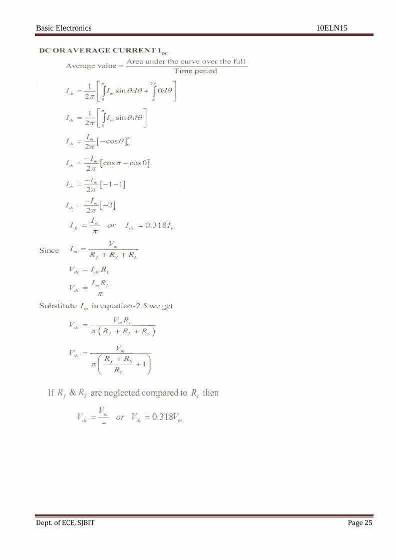
It is defined as the ratio of the RMS voltage across output to the average dc component.

Basic Electronics 10ELN15
Dept. of ECE, SJBIT Page 31
The PIV rating of the diode is given by manufacturer and the diode should be operated below its PIV.If
the max. voltage across the secondary of the transformer exceeds PIV of the diode then the diode will
get damaged.
For HWR the PIV under reverse bias condition is Vm.
Advantage and disadvantages of HWR.
Advantage: 1.The circuit is simpler and requires only one diode.
2. PIV of the diode is only Vm.
Disadvantages: 1. The ripple is more and hence the ripple factor is also more(12%)
2 Efficiency is very low.(40.6%)
Low TUF (28.7%
Basic Electronics 10ELN15
Dept. of ECE, SJBIT Page 32
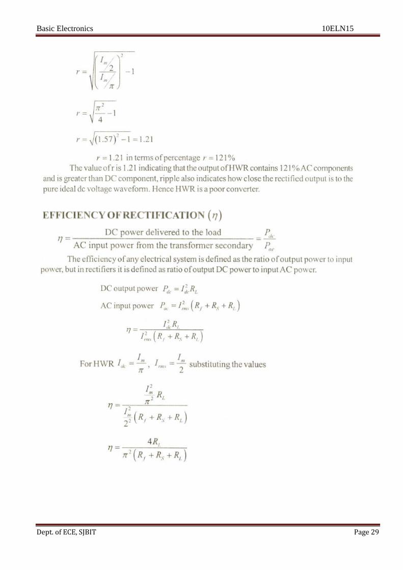
Full-wave rectifier
Full-wave rectifier is of two types
1. Centre tapped full-wave rectifier
2. Bridge rectifier
Centre tapped full –wave rectifier
Fig. 1.26 Centre tapped full-wave rectifier
Fig. 1.27 Full wave rectifier, fig-a full wave rectifier circuit, fig-b when diodes are conducting and, fig-c, when
diode s are not conducting.
The circuit diagram of a center tapped full wave rectifier is shown in fig. 1.26 above. It employs
two diodes and a center tap transformer. The a.c. signal to be rectified is applied to the primary
of the transformer and the d.c. output is taken across the load RL.
Basic Electronics 10ELN15
Dept. of ECE, SJBIT Page 33
During the +ve half-cycle end X is +ve and end Y is –ve this makes diode D1 forward biased
and thus a current i1 flows through it and load resistor RL.Diode D2 is reverse biased and the
current i2 is zero.
During the –ve half-cycle end Y is +Ve and end X is –Ve. Now diode D2 is forward biased and
thus a current i2 flows through it and load resistor RL. Diode D1 is reversed and the current i1 = 0.
Advantages
Efficiency is high, (81.2%).
Low ripple, ripple factor is 48.2%.
Requires only two diodes.
Disadvantages
Since, each diode uses only one-half of the transformer secondary voltage the d.c. output is
comparatively small.
The diodes used must have high Peak-inverse voltage, PIV=2Vm.
Requirement of a special-centre tapped- transformer
Bridge rectifier
(i)
Vout
D1D3 D2D4 D1D3
t
Fig.1.28 Full wave bridge wave rectifier (i) Circuit diagram (ii) waveforms.
The circuit diagram of a bridge rectifer is shown above. It uses four diodes and a transformer.
During the +ve half-cycle, end A is +ve and end B is –ve thus diodes D1 and D3 are forward bias
while diodes D2 and D4 are reverse biased thus a current flows through diode D1, load RL ( C to D)
and diode D3.

Basic Electronics 10ELN15
Dept. of ECE, SJBIT Page 34
During the –ve half-cycle, end B is +ve and end A is –ve thus diodes D2 and D4 are forward
biased while the diodes D1 and D3 are reverse biased. Now the flow of current is through diode
D4 load RL ( D to C) and diode D2. Thus, the waveform is same as in the case of center-tapped
full wave rectifier.
Advantages
The need for center-taped transformer is eliminated.
The output is twice when compared to center-tapped full wave rectifier.
for the same secondary voltage.
The peak inverse voltage is one-half(1/2) compared to center-tapped full wave rectifier.
Can be used where large amount of power is required.
Disadvantages
It requires four diodes.
The use of two extra diodes cause an additional voltage drop thereby reducing the output voltage.
Analysis of Full Wave Rectifier (FWR)
The analysis of FWR‘s –center tap construction or bridge construction- is same except for minor
changes.
The full wave rectifier (FWR), will have 48.2% ripple. Comparing this with that of HWR which is
121%, we find that the ripple factor is better for FWR.
Efficiency of Full-wave rectifier
Let V = Vmsinθ be the voltage across the secondary winding
I = Imsinθ be the current flowing in secondary circuit
rf = diode resistance
RL = load resistance
dc power output
LdcRIPdc 2 -----------------------------(1)
0
.2
12 diII avdc
0
.Im2
12 dSinI av
m
av
II
2 -------------------------------------------------------- (2)
Efficiency of Full-wave rectifier

Basic Electronics 10ELN15
Dept. of ECE, SJBIT Page 35
Let V = Vmsinθ be the voltage across the secondary winding
I = Imsinθ be the current flowing in secondary circuit
rf = diode resistance
RL = load resistance
Efficiency=dc power output/acpower input=Pdc/Pac
dc power output
LdcRIPdc 2 -----------------------------(1)
0
.2
12 diII avdc
0
.Im2
12 dSinI av
m
av
II
2 -------------------------------------------------------- (2)
L
m
dc RI
P
22
------------------------------------------ (3)
input ac power
Lfrmsac RrIP 2
---------------------------------------- (4)
diI rms 0
2
2
12
Squaring both sides we get
diI rms 0
22 1
2
2
2 m
rms
II
2
m
rms
II ------------------------------------------------ ----- (5)
Lf
m
ac RrI
P
2
2 --------------------------------------------(6)
Lf
L
m
m
ac
dc
Rr
R
I
I
P
P
*
2
22
2
0
22 )(Im1
dSinI rms

Basic Electronics 10ELN15
Dept. of ECE, SJBIT Page 36
η =
L
f
R
r1
812.0 -------------------------------------------------(7)
The efficiency will be maximum if rf is negligible as compared to RL.
Maximum efficiency = 81.2 %
This is the double the efficiency due to half wave rectifier. Therefore a Full-wave rectifier is twice as
effective as a half-wave rectifier
Comparision of Rectifiers
Particulars Half wave rectifier Centre-tapped Full
wave rectifier
Bridge rectifier
1. No. of diodes
2. Idc
3. Vdc
4.Irms
5.Efficiency
6.PIV
7.Ripple factor
1
Im / Π
Vm / Π
Im / 2
40.6 %
Vm
1.21
2
2Im /Π
2Vm / Π
Im /√ 2
81.2 %
2Vm
0.48
4
2Im /Π
2Vm / Π
Im /√ 2
81.2 %
Vm
0.48
Note:
The relation between turns ratio and voltages of primary and secondary of the transformer is
given by
o N1 / N2 = Vp / Vs
RMS value of voltage and Max. value of voltage is related by the equation.
Vrms = Vm / √2 ( for full-cycle of ac)
If the type of diode is not specified then assume the diode to be of silicon type.
For an ideal diode, forward resistance rf = 0 and cut-in voltage , Vγ = 0.
The Transformer Utilization Factor (TUF) for full wave rectifier is 81.2%,which is better compared to
HWR,for which it is only28.7%.

Basic Electronics 10ELN15
Dept. of ECE, SJBIT Page 37
Peak Inverse Voltage(PIV): For the center tapped transformer if any one diode is conducting the
voltage across it is the entire secondary voltage of the transformer which is Vm.+ Vm.=2Vm.Therefore the
diodes used in the center tap design should have a PIV of 2Vm.
Whereas in the bridge configuration the PIV of each diode is only Vm
Note:
The relation between turns ratio and voltages of primary and secondary of the transformer is given by
N1 / N2 = Vp / Vs
RMS value of voltage and Max. value of voltage is related by the equation.
Vrms = Vm / √2 ( for full-cycle of ac)
If the type of diode is not specified then assume the diode to be of silicon type.
For an ideal diode, forward resistance rf = 0 and cut-in voltage , Vγ = 0.
Questions
1. Explain the quantitative theory of p-n junction. ----------------------------------------Feb.
2006,7Marks
2. With the help of the diode equation, explain the V-I characteristics of p-n junction—Aug.8Marks
3. Explain the V-I characteristics with respect to the current equation---------Aug. 2004, 6Marks
4. Draw and explain V-I characteristics of p-n junction diode –Feb.2004,5 Marks
5. write the current equation of a p-n junction and explain the V-I characteristics. What is the effect
of temperature on cut-in voltage and reverse saturation current?-----Aug 2003,8 Marks
6. Differentiate between Zener breakdown and Avalanche breakdown—Aug. 2002, 5 Marks.
7. Draw and explain V-I characteristics of a p-n junction diode.--------- Aug. 2001, 5 Marks
8. Draw the volt- ampere characteristics of a silicon diode marking the cut-in voltage. Briefly
explain the V-I characteristics with respect to the diode current equation.-------------March 2001,
5 Marks.
9. Draw and explain the V-I characteristics of silicon and germanium diodes.----Aug. 2000,5Marks.
10. Write the diode equation and explain the significance of the terms.—March 2000,5Marks
DIODE APPLICATIONS
1. Define ripple factor show from first principles R.F.of a H.W.R.is1.21--------Feb.2006,7Marks
2. Draw and explain the working of bridge type F.W.R with necessary waveforms. Derive the
expression for Idc and η.----------------------------------Aug. 2004,10Marks
Basic Electronics 10ELN15
Dept. of ECE, SJBIT Page 38
3. Design the zener regulator for the following specifications----------------------Feb. 2004,5
NMarks
4. Output voltage = 5V
Load current = 20Ma
Zener wattage = 500mW
Input voltage = 125± 3V
5. Draw the bridge rectifier circuit and explain its operation with wave form-Feb 2004,5Marks
6. Explain the working of a full wave bridge rectifier with the help of circuit diagram and wave
forms:Also derive the expression for Vdc. ---------------Aug 2003, 9 Marks
============= 0 =============
Example 1 :In a bridge type FWR, the transformer secondary voltage is 100sinώt.The forward
resistance of each diode is 25Ω and the load resistance is 950Ω.Calculate
i)dc output voltage,ii)ripple factor,iii)efficiency of rectification,iv)PIV of diodes.
-----Jan/Feb-2005
Given, v=100sinώt=Vm sinώt
Hence Vm.=100Volts
.
FILTERS
We know that the output of the rectifier is pulsating d.c. ie the output obtained by the rectifier is not pure
d.c. but it contains some ac components along with the dc o/p. These ac components are called as
Ripples, which are undesirable or unwanted. To minimize the ripples in the rectifier output filter circuits
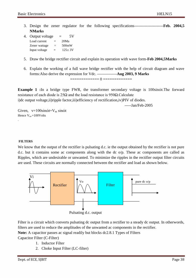
are used. These circuits are normally connected between the rectifier and load as shown below.
Vi
Vo pure dc o/p
Pulsating d.c. output
Filter is a circuit which converts pulsating dc output from a rectifier to a steady dc output. In otherwords,
filters are used to reduce the amplitudes of the unwanted ac components in the rectifier.
Note: A capacitor passes ac signal readily but blocks dc2.8.1 Types of Filters
Capacitor Filter (C-Filter)
1. Inductor Filter
2. Choke Input Filter (LC-filter)
Rectifier
Filter

Basic Electronics 10ELN15
Dept. of ECE, SJBIT Page 39
3. Capacitor Input Filter (Π-filter)
Capacitor Filter( C-filter)
Vin
a f
e
t
b d
c
V1
with filter a
e
t
Fig.1.29 Capacitor filter ( C-filter) (i) Circuit diagram (ii) waveforms
When the Input signal rises from o to a the diode is forward biased therefore it starts conducting
since the capacitor acts as a short circuit for ac signal it gets charged up to the peak of the input
signal and the dc component flows through the load RL.
When the input signal fall from a to b the diode gets reverse biased . This is mainly because of
the voltage across the capacitor obtained during the period o to a is more when comapared to Vi.
Therefore there is no conduction of current through the diode.
Now the charged capacitor acts as a battery and it starts discharging through the load RL. Mean
while the input signal passes through b,c,d section. When the signal reaches the point d the diode
is still reverse biased since the capacitor voltage is more than the input voltage.
When the signal reaches point e, the input voltage can be expected to be more than the capacitor
voltage. When the input signal moves from e to f the capacitor gets charged to its peak value
again. The diode gets reverse biased and the capacitorstarts discharging. The final output across
RL is shown in Fig. 2.

Basic Electronics 10ELN15
Dept. of ECE, SJBIT Page 40
The ripple factor for a Half-wave rectifier with C-filer is given by
r= 1/2√3fCRL
f-----the line frequency ( Hz); C-----capacitance ( F);RL------- Load resistance (Ω);
Ripple factor for full-wave rectifier with C-filter is given by r = 1/ 4 √3 f C RL
Advantages of C-Filter
low cost, small size and good characteristics.
It is preferred for small load currents ( upto 50 mA)
It is commonly used in transistor radio, batteries eliminator etc.
Zener voltage regulator.
The zener diode: The circuit diagram of Zener voltage regulator is shown below
Fig. 1.30 Zener voltage regulator
The zener diode of breakdown voltage VZ is connected in reverse biased condition across the load RL
such that it operates in breakdown region. Any fluctuations in the current are absorbed by the series
resistance Rs. The Zener will maintain a constant voltage VZ
( equal to Vo) across the load unless the input voltage does not fall below the zener breakdown voltage
VZ.
Case(i): When input voltage Vin varies and RL is constant
If the input voltage increases, the Zener diode which is in the breakdown region is equivalent to
a battery VZ as shown in figure. The output voltage remains constant at VZ (equal to Vo) and the excess
voltage is dropped across the series resistance RS. We know that for a zener diode under breakdown
region large change in current produces very small change in voltage, thereby the output voltage remains
constant.
Case (ii):When Vin is constant and RL varies.

Basic Electronics 10ELN15
Dept. of ECE, SJBIT Page 41
If there is a decrease in the load resistance RL and the input voltage remains constant then there is an
increase in load current.
Since Vin is constant the current cannot come from the source. This addition load current is driven from
the battery VZ and we know that even for a large decrease in current the Zener output voltage Vz remains
same. Hence the output voltage across the load is also constant..
Hence for the zener circuit to work as a regulator,the following condition must be satisfied :
Zener must be reverse biased.
Input voltage must be greater than the zener voltage.(to ensure zener breakdown)
The load current must be less than maximum zener current, Iz(max)---this is due to the fact that
when the load is removed this much current flows through zener,therefore it should not exceed
zener max. current.
The current limiting resistance Rs shall be selected such that Iz should be within the limits of Iz max and
Izmin.That is Izmin<Iz<Izmax
Working:
Case 1: When input voltage increases i.e.Vi≥Vz, then the zener is in the breakdown region and voltage
across it remains constant.The current through it increases.This increases the current through the
resulting more voltage drop across it (i.e.Is*Rs).Thus compensating increase in Vi.
Case 2: if load increases (i.e RL decreases ).This extra current cannot be supplied by the input (since Vi
is constant).This is by decreasing zener current level.The current through Rs is constant.Therefore the
output remains constant.
Designing of Rs: Since the current through the zener varies with the change in input voltage.The value of
Rs to limit this current has to be chosen such that,the zener max. and min. current are limited.
Iz max. is decided by Pz (power dissipation of zener) of zenerand Rsmin.≤Rs≤Rz max.
Iz min is decided by min. current required for breakdown.
Recommended questions:
1. Explain the VI- characteristics of a pn-junction diode.
2.Sketch the typical V-I characteristics of PN junction diode and identify the important points.
3.Draw and explain the V-I characteristics of Si and Ge diodes.
4.Derive an expression for the ripple factor and efficiency of half wave rectifier (HWR).
------------------ 0 -----------------

Basic Electronics 10ELN15
Dept. of ECE, SJBIT Page 42
Unit -2 TRANSISTORS
A transistor is a sandwich of one type of semiconductor (P-type or n-type) between two layers of other
types.
Transistors are classified into two types;
1. pnp transistor
pnp transistor is obtained when a n-type layer of silicon is sandwiched between two p-type
silicon material.
2. npn transisitor
npn transistor is obtained when a p-type layer of silicon is sandwiched between two n-type
silicon materials.
Figure2.1 below shows the schematic representations of a transistor which is equivalent of two
diodes connected back to back.
JE JC JE JC
E C E C
B B
Fig 2.1: Symbolic representation
pnp npn
Fig 2.2: Schematic representation
The three portions of transistors are named as emitter, base and collector. The junction between
emitter and base is called emitter-base junction while the junction between the collector and base is
called collector-base junction.
The base is thin and tightly doped, the emitter is heavily doped and it is wider when compared to
base, the width of the collector is more when compared to both base and emitter.
n n
p
p p
n

Basic Electronics 10ELN15
Dept. of ECE, SJBIT Page 43
In order to distinguish the emitter and collector an arrow is included in the emitter. The direction of
the arrow depends on the conventional flow of current when emitter base junction is forward biased.
In a pnp transistor when the emitter junction is forward biased the flow of current is from emitter to
base hence, the arrow in the emitter of pnp points towards the base.
Operating regions of a transistor
A transistor can be operated in three different regions as
a) active region
b) saturation region
c) cut-off region
Active region
E JE B JC C
VEB VCB
Fig 2.3: pnp transistor operated in active region
The transistor is said to be operated in active region when the emitter-base junction is
forward biased and collector –base junction is reverse biased. The collector current is said to have two
current components one is due to the forward biasing of EB junction and the other is due to reverse
biasing of CB junction. The collector current component due to the reverse biasing of the collector
junction is called reverse saturation current (ICO or ICBO) and it is very small in magnitude.
Saturation region
E JE B JC C
VEB VCB
Fig 2.4: pnp transistor operated in Saturation region
Transistor is said to be operated in saturation region when both EB junction and CB junction are forward
biased as shown. When transistor is operated in saturation region IC increases rapidly for a very small
change in VC.
p p
n
p p
n

Basic Electronics 10ELN15
Dept. of ECE, SJBIT Page 44
Cut-off region
E JE B JC C
VEB VCB
Fig 2.5: pnp transistor operated in Cut-off region
When both EB junction and CB junction are reverse biased, the transistor is said to be operated in cut-off
region. In this region, the current in the transistor is very small and thus when a transistor in this region it
is assumed to be in off state.
Working of a transistor (pnp)
E JE B JC C
IE IC
IB
VEB VCB
Fig 2.6 Transistor in active region
Consider a pnp transistor operated in active region as shown in Figure 2.6
Since the EB junction is forward biased large number of holes present in the emitter as
majority carriers are repelled by the +ve potential of the supply voltage VEB and they move
towards the base region causing emitter current IE.
Since the base is thin and lightly doped very few of the holes coming from the emitter
recombine with the electrons causing base current IB and all the remaining holes move
towards the collector. Since the CB junction is reverse biased all the holes are immediately
attracted by the –ve potential of the supply VCB. Thereby giving rise to collector current IC.
Thus we see that IE = IB + IC -----------------(1) (By KVL)
Since the CB junction is reverse biased a small minority carrier current ICO flows from base
to collector.
p p
n
IE IC
p p ICO
n

Basic Electronics 10ELN15
Dept. of ECE, SJBIT Page 45
Current components of a transistor
JE JC
IE
IC
IB
VEB VCB
Fig 2.7: Current components of a transistor
Fig 2.7 above shows a transistor operated in active region. It can be noted from the diagram the battery
VEB forward biases the EB junction while the battery VCB reverse biases the CB junction.
As the EB junction is forward biased the holes from emitter region flow towards the base causing a hole
current IPE. At the same time, the electrons from base region flow towards the emitter causing an
electron current INE. Sum of these two currents constitute an emitter current IE = IPE +INE.
The ratio of hole current IPE to electron current INE is directly proportional to the ratio of the conductivity
of the p-type material to that of n-type material. Since, emitter is highly doped when compared to base;
the emitter current consists almost entirely of holes.
Not all the holes, crossing EB junction reach the CB junction because some of the them combine with
the electrons in the n-type base. If IPC is the hole current at (Jc) CB junction. There will be a
recombination current IPE - IPC leaving the base as shown in figure 3.7.
If emitter is open circuited, no charge carriers are injected from emitter into the base and hence emitter
current IE =o. Under this condition CB junction acts a a reverse biased diode and therefore the collector
current ( IC = ICO) will be equal to te reverse saturation current. Therefore when EB junction is forward
biased and collector base junction is reverse biased the total collector current IC = IPC +ICO.
Transistor configuration
We know that, transistor can be used as an amplifier. For an amplifier, two terminals are required to
supply the weak signal and two terminals to collect the amplified signal. Thus four terminals are
required but a transistor is said to have only three terminals Therefore, one terminal is used common for
both input and output.
IPE IPC
(hole current) (hole current)
INE (e- current) ICO
IPB

Basic Electronics 10ELN15
Dept. of ECE, SJBIT Page 46
This gives rise to three different combinations.
1. Common base configuration (CB)
2. Common emitter configuration (CE)
3. Common collector configuration (CC)
1. CB configuration
A simple circuit arrangement of CB configuration for pnp transistor is shown below.
IE IC
Vi IB RL Vout
VEB VCB
Fig 2.8:CB configuration
In this configuration, base is used as common to both input and output. It can be noted that the i/p
section has an a.c. source Vi along with the d.c. source VEB. The purpose of including VEB is to keep EB
junction always forward biased (because if there is no VEB then the EB junction is forward biased only
during the +ve half-cycle of the i/p and reverse biased during the –ve half cycle). In CB configuration, IE
–i/p current, IC –o/p current.
Current relations
1.current amplification factor (α)
It is defined as the ratio of d.c. collector current to d.c. emitter current
α = E
O
I
I
2. Total o/p current
We know that CB junction is reverse biased and because of minority charge carriers a small reverse
saturation current ICO flows from base to collector.
IC = IE + ICO
Since a portion of emitter current IE flows through the base ,let remaining emitter current be αIE .
IC = αIE + ICo
Characteristics
1. Input characteristics
Basic Electronics 10ELN15
Dept. of ECE, SJBIT Page 47
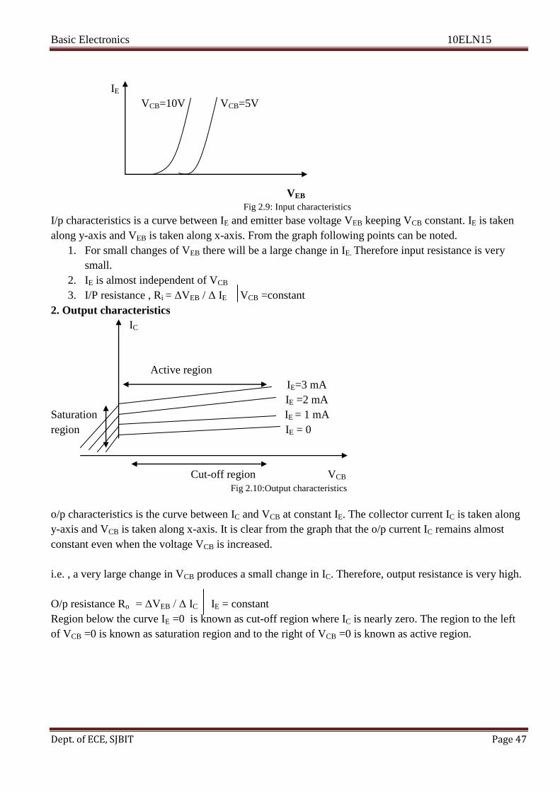
IE
VCB=10V VCB=5V
VEB
Fig 2.9: Input characteristics
I/p characteristics is a curve between IE and emitter base voltage VEB keeping VCB constant. IE is taken
along y-axis and VEB is taken along x-axis. From the graph following points can be noted.
1. For small changes of VEB there will be a large change in IE. Therefore input resistance is very
small.
2. IE is almost independent of VCB
3. I/P resistance , Ri = ΔVEB / Δ IE VCB =constant
2. Output characteristics
IC
Active region
IE=3 mA
IE =2 mA
Saturation IE = 1 mA
region IE = 0
Cut-off region VCB
Fig 2.10:Output characteristics
o/p characteristics is the curve between IC and VCB at constant IE. The collector current IC is taken along
y-axis and VCB is taken along x-axis. It is clear from the graph that the o/p current IC remains almost
constant even when the voltage VCB is increased.
i.e. , a very large change in VCB produces a small change in IC. Therefore, output resistance is very high.
O/p resistance Ro = ΔVEB / Δ IC IE = constant
Region below the curve IE =0 is known as cut-off region where IC is nearly zero. The region to the left
of VCB =0 is known as saturation region and to the right of VCB =0 is known as active region.
Basic Electronics 10ELN15
Dept. of ECE, SJBIT Page 48
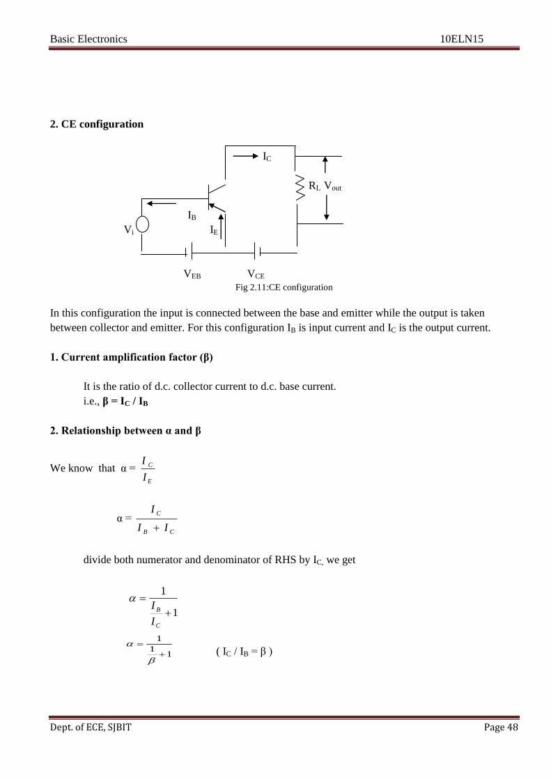
2. CE configuration
IC
RL Vout
IB
Vi IE
VEB VCE
Fig 2.11:CE configuration
In this configuration the input is connected between the base and emitter while the output is taken
between collector and emitter. For this configuration IB is input current and IC is the output current.
1. Current amplification factor (β)
It is the ratio of d.c. collector current to d.c. base current.
i.e., β = IC / IB
2. Relationship between α and β
We know that α = E
C
I
I
α = CB
C
II
I
divide both numerator and denominator of RHS by IC, we get
1
1
C
B
I
I
( IC / IB = β )
11
1

Basic Electronics 10ELN15
Dept. of ECE, SJBIT Page 49
1
Also we have
1
)1(
)1(
Derivation of Total output current IC
We have CBOEC III
1
)1(
1
CBOEC
CBOEC
III
IIB
I
Ic = CBOB II )1(
Transistor Characteristics
1. i/p characteristics
IB
VCE=10V VCE=5V
VEB
Fig 2.11: i/p characteristics
Input characteristics is a curve between EB voltage (VEB ) and base current (IB ) at constant VCE. From
the graph following can be noted.
1. The input characteristic resembles the forward characteristics of a p-n junction diode.
2. For small changes of VEB there will be a large change in base current IB. i.e., input resistance is
very small.
3. The base current is almost independent of VCE.
4. Input resistance , Ri = ΔVEB / Δ IB V CE = constant
2. Output characteristics

Basic Electronics 10ELN15
Dept. of ECE, SJBIT Page 50
IC
(mA)
Active region
30 μA
20 μA
10 μA
IB =0μA
Cut-off region
V CE(volts)
Fig 2.12: Output characteristics
It is the curve between VCE and IC at constant IB. From the graph we can see that,
1. Very large changes of VCE produces a small change in IC i.e output resistance is very high.
2. output resistance Ro = ΔVCE / ΔIC IB = constant
Region between the curve IB =0 is called cut-off region where IB is nearly zero. Similarly the active
region and saturation region is shown on the graph.
3. CC configuration
IE
RL Vout
IB
Vi IC
VCB VCE
Fig 2.13: CC configuration
In this configuration the input is connected between the base and collector while the output is taken
between emitter and collector.
Here IB is the input current and IE is the output current.
Current relations
1. Current amplification factor (γ)
2. Relationship between α β and γ
γ = B
E
I
I

Basic Electronics 10ELN15
Dept. of ECE, SJBIT Page 51
γ = B
CB
I
II
divide both Numerator and denominator by IB
1
1B
C
II
1 ( β = IC / IB)
11
1
1
Derivation of total output current IE
We know that IC = CBOE II
IE = IB + IC
IE = IB + αIE + ICBO
IE(1-α ) = IB + ICBO
IE =
11
CBOB II
IE = γIB + γICBO
IE = γ (IB + ICBO)

Basic Electronics 10ELN15
Dept. of ECE, SJBIT Page 52
Comparison between CB, CC and CE configuration
Characteristics CB CE CC
1. Input reistance (Ri)
2. Output resistance (Ro)
3. Current amplification
factor
4. Total output current
5. Phase relationship
between input and output
6. Applications
7. Current gain
8. Voltage gain
low
high
1
CBOEC III
In-phase
For high frequency
applications
Less than unity
Very high
low
high
1
Ic = CBOB II )1(
Out-of phase
For audio frequency
applications
Greater than unity
Grater than unity
high
low
1
1
IE = γIB + γICBO
in-phase
For impedance
matching
Very high
Less than unity
Transistor as an amplifier
IC
RL Vout
IB
Vi ` IE
VEB VCB
Fig 2.14: Transistor as an amplifier

Basic Electronics 10ELN15
Dept. of ECE, SJBIT Page 53
Consider a npn transistor in CE configuration as shown above along with its input characteristics.
A transistor raises the strength of a weak input signal and thus acts as an amplifier. The weak signal to
be amplified is applied between emitter and base and the output is taken across the load resistor RC
connected in the collector circuit.
In order to use a transistor as an amplifier it should be operated in active region i.e. emitter junction
should be always FB and collector junction should be RB. Therefore in addition to the a.c. input source
Vi two d.c. voltages VEB and VCE are applied as shown. This d.c. voltage is called bias voltage.
As the input circuit has low resistance, a small change in te signal voltage Vi causes a large change in the
base current thereby causing the same change in collector current (because IC = βIB).
The collector current flowing through a high load resistance RC produces a large voltage across it. Thus a
weak signal applied at the input circuit appears in the amplified form at the output. In this way transistor
acts as an amplifier.
Example: Let RC = 5KΩ, Vin =1V, IC =1mA then output V=ICRC =5V
mass system illustrates some important and universal principles of osc2. CE configuration
IC
RL Vout
IB
Vi IE
VEB VCE
Fig 2.15:CE configuration
In this configuration the input is connected between the base and emitter while the output is taken
between collector and emitter. For this configuration IB is input current and IC is the output current.
1. Current amplification factor (β)
It is the ratio of d.c. collector current to d.c. base current.
i.e., β = IC / IB
2. Relationship between α and β
We know that α = E
C
I
I

Basic Electronics 10ELN15
Dept. of ECE, SJBIT Page 54
α = CB
C
II
I
divide both numerator and denominator of RHS by IC, we get
1
1
C
B
I
I
( IC / IB = β )
1
Also we have
1
)1(
)1(
Derivation of Total output current IC
We have CBOEC III
1
)1(
1
CBOEC
CBOEC
III
IIB
I
Ic = CBOB II )1(
11
1

Basic Electronics 10ELN15
Dept. of ECE, SJBIT Page 55
Transistor Characteristics
1. i/p characteristics
IB
VCE=10V VCE=5V
VEB
Fig 2.16: i/p characteristics
Input characteristics is a curve between EB voltage (VEB ) and base current (IB ) at constant VCE. From
the graph following can be noted.
The input characteristic resembles the forward characteristics of a p-n junction diode.
For small changes of VEB there will be a large change in base current IB. i.e., input
resistance is very small.
The base current is almost independent of VCE.
Input resistance , Ri = ΔVEB / Δ IB V CE = constant
2. Output characteristics
IC
(mA)
Active region
30 μA
20 μA
10 μA
IB =0μA
Cut-off region
V CE(volts)
Fig 2.17: Output characteristics
It is the curve between VCE and IC at constant IB. From the graph we can see that,
Very large changes of VCE produces a small change in IC i.e output resistance is very high.
output resistance Ro = ΔVCE / ΔIC IB = constant
Region between the curve IB =0 is called cut-off region where IB is nearly zero. Similarly the active
region and saturation region is shown on the graph.
3. A) Define alpha and beta of a transistor and derive the relationship between them
B) Sketch the input characteristics of transistor in CC configuration.

Basic Electronics 10ELN15
Dept. of ECE, SJBIT Page 56
Ans:A)
Relationship between α and β
We know that α = E
C
I
I
α = CB
C
II
I
divide both numerator and denominator of RHS by IC, we get
1
1
C
B
I
I
( IC / IB = β )
1
Also we have
1
)1(
)1(
B)the input characteristics of common collector stage is driven by the equation
VCE = VBE + VCB.
In order to draw the input characteristics the output voltage in this case vce is held constant and vbe is
also constant the forward diode drop the input voltage is nothing but vce-vbe, if this condition is violated
zero current flows through the transistor.
UNIT-3
BIASING METHODS
Biasing:
11
1

Basic Electronics 10ELN15
Dept. of ECE, SJBIT Page 57
Transistor biasing is the establishment of suitable dc values such as Ic, VCE, IB etc. by using a
single dc source... When BJT is properly biased, faithful amplification of signals take place. For example
applying forward bias to EB- junction and reverse bias to the CB-junction makes the transistor to operate
in the active region. Hence Biasing is applying dc voltages to the junctions of the transistor to make it
operate in the desired region. Biasing eliminates the need for separate dc sources in the emitter and
collector circuits.
Types of biasing.
There are mainly three types of biasing circuits used for biasing a transistor, they are:
a) Base bias or fixed bias
b) Collector to base bias
c) Voltage divider bias
The three biasing circuits are shown in figure 3.1
Fig3.1 : The three basic biasing circuits.
a) Base bias or fixed bias:
For this configuration the biasing arrangement is as shown in figure3.2 below. A base resistance RB is
used between Vcc and base to establish the base current IB Thus the base current is the constant quantity
determined by Vcc and IB. Because Vcc and RB are fixed quantities, IB remains fixed and hence it is also
called fixed bias.

Basic Electronics 10ELN15
Dept. of ECE, SJBIT Page 58
Fig 3.2: Base bias circuit.
Applyingh Kirchoff‘s voltage law to the base circuirt. (The base circuit consists of Vcc, RB,EB- junction
of the transistor and ground)
IB RB +VBE=Vcc
IB =(Vcc- VBE)/ RB
VBE is 0.7V for Silicon and 0.3V for Germanium transistor.
The collector current is calculated as
Ic= β IB.
Applying the KVL to collector circuit (The collector circuit consists of Vcc, Rc, VCE, and ground
Vcc= VCE +IcRc
VCE =Vcc –IcRc
Example: The base bias circuit is shown in fig 3.3.For the values indicated calculate IB, Ic and VCE.
Example1:
Fig-3.3

Basic Electronics 10ELN15
Dept. of ECE, SJBIT Page 59
Effect of hFE(max) and hPE(mifl)
When the transistor de current gain is known. it is quite easy to determine the circuit bias conditions
exactly as in However.in practise the precise current gain of each transistor is normallynot known. The
transistor is usually identified by its type number. and then the maximum and minimum values of current
gain can be obtained from the manufacturer's data sheet. In circuit analysis it is sometimes convenient to
use a typical Hfe value. However. as demonstrated in Example 5-4. hFElmaxl and hpElf11il11must be
used to calculate the range of possible levels of Ic
and VCE'
Example2:
Figure 3:
Note that the typichFE value of 100 used in Ex. 5-3 gives Ic =3.68 mA and VCE = 9.9 V. But. applying
the hFElf11inl and hFElmaxl values in Example 4-4 results in an Ic range of 1.84 mA to 7.36 mAl and
VCE ranging from 1.8 V to 13.95 V. The different Ic and VCE levels determined in Examples 3.1 and3.

Basic Electronics 10ELN15
Dept. of ECE, SJBIT Page 60
2 are illustrated by the three Q points in Fig. 3.4 Transistors of a given type number always have a wide
range of hFE values (the hFE spread). So
hFE(maxand hFE(minshould always be used for practical circuit analysis.
The base bias Circuit is rarely employed because of the uncertainty of the Q point. More predictable
results can be obtained with other types of bias circuit.
Fig 3.4: The transistor hFE value has a major effect on the Q p0int for a base bias circuit.
Base bias using pnp transistor:
All of the base bias circuit discussed for npn is also applicable for pnp transistor except for polarities
of voltage and currents. The figure shows the pnp transistor biasing circuit. Note that the voltage
polarities and current directions are reversed compared to npn transistor base bias circuit. The KVL
equations can be applied for analyzing the pnp transistors base bias circuit in exactly the same way as
for npn circuits discussed above.
Fig 3.5: Base bias circuits using pnp transistors.
b)Collector to base bias circuit:
Circuit operation and analysis:
The collector-to-base bias circuit shown in Fig.5-17(a) has the base resistor RB connected between the
transistor collector and base terminals. As will be demonstrated. this circuit has significantly

Basic Electronics 10ELN15
Dept. of ECE, SJBIT Page 61
improvedbias stability for hpE changes compared to base bias. Refer to Fig. 5-17(b) and note that the
voltage across RB is dependent on VeE•
Fig 3.6: Collector-to-base bias circuits. Any change in VCE changes IB The IB change causes IC to
change, and this tends to return IC toward its original level.
Note that the voltage across RB. is dependent on VCE and VCE is independent of the level of Ic and IB.
If Ic increases above the design level there is an increased voltage drop across Rc, resulting in a
reduction in VCE..The reduced Vce level causes IB to be lower than its design level and because Ic= β Ib,
the collector current is also reduced. Thus, an increase in Ic produces a feedback effect that tends to
return Ic toward its original level. Similarly, reduction in Ic produces an increase in Vce which increase
IB, thus tending to increase Ic back to the original level.
Analysis of this circuit is a little more complicated than base bias analysis. To simplify the process an
equation is first derived for the base current IB.. Equating equations 1 and 2,
Hence, VCE = Vcc-Rc (IB +Ic) = VBE + IB RB
IB (Rc + RB ) + Ic Rc = Vcc- VBE
Substituting Ic = β IB into the above equation
IB (Rc + RB ) + β IBRc = Vcc- VBE
This gives
Vcc- VBE
IB = ------------- ------------------- 3
(β + 1) Rc + RB

Basic Electronics 10ELN15
Dept. of ECE, SJBIT Page 62
Effect of β (max) and β (min) in collector to base bias circuit
In the collector to base bias circuit, the feed back from the collector from the collector to base reduces
the effects of β spread values, due to transistor replacement etc. Thus collector to base bias has greater
stability than base bias for a given range of β values. This is illustrated in the following example.
It is important to note that, unlike the situation in a base bias circuit, the base current in a
collector to base bias circuit does not remain constant, rather IB compensates for IC increase due to
negative feed back provided by the base bias resistor RB, even when the transistor β value is changed as
illustrated in the following example.
Comparing the base bias and the collector to base bias circuits for Q point stabilization against β
variations, it is seen that the Q points for the collector to bias circuit is clearly has greater stability
against β spread value than base bias circuit.
Collector to base bias circuit using pnp transistor.
Collector to base bias circuit using pnp transistor. is illustrated in fig. below. Note that the voltage
polarities and current directions are reversed compared to npn transistor collector to base bias circuit.
This circuit can be analyzed in exactly the same way as the npn transistor circuit.
Voltage divider bias circuit
Circuit operation
Voltage divider bias also known as emitter current bias, is the most stable of the three basic transistor
biasing circuits. A voltage divider bias circuit is shown in fig. below, and the current and voltage
conditions through out the discussions are illustrated in fig.8. It is seen that there is an emitter resistor RE
connected in series with emitter, so that the total dc load in series with the transistor is (Rc+ RE) and this
resistance must be used when drawing the dc load line for the circuit. Resistor R1 and R2 constitute a
voltage divider that divides the supply voltage to produce the base bias voltage IB.
Voltage divider bias circuits are normally designed to have the voltage divider current (I2) very much
larger than the transistor base current (IB).In this circumstance, VBE is largely affected by IB so VBE can
be assumed to remain constant.

Basic Electronics 10ELN15
Dept. of ECE, SJBIT Page 63
Fig.-3.7 : Voltage divider bias circuit.
Referring to above figure 8, with VB constant, the voltage across the emitter resistor is also a constant
quantity; this means that the emitter current is constant,
The collector current is approximately equal to the emitter current, so Ic is held at constant level. Again
referring to the figure, the transistor collector to emitter voltage is,
VCE = Vcc- (IC + IB) RC
Clearly, with Ic and IE constant, the transistor collector- emitter voltage remains at a constant level.
It should be noted that the transistor β value is not involved in any of the above equations.
The effect of max. and min. β in voltage divider bias circuit
The following example will demonstrate the variation of β with transistor replacements. The variations
of β on the operating point Q is much less than the C-B bias. Hence this biasing technique is more
reliable and stable. This makes it the most popular and preferred biasing technique used in circuits.
Comparison of varies biasing techniques.
a) Base bias circuit: The stability of this circuit is less. No feed back is used. Used only where
stability is not important like switching circuits.
b) Collector to base bias: Moderately used, has moderate stability.Negetive feedback is used. It is
used in switching applications where moderate stability is essential.
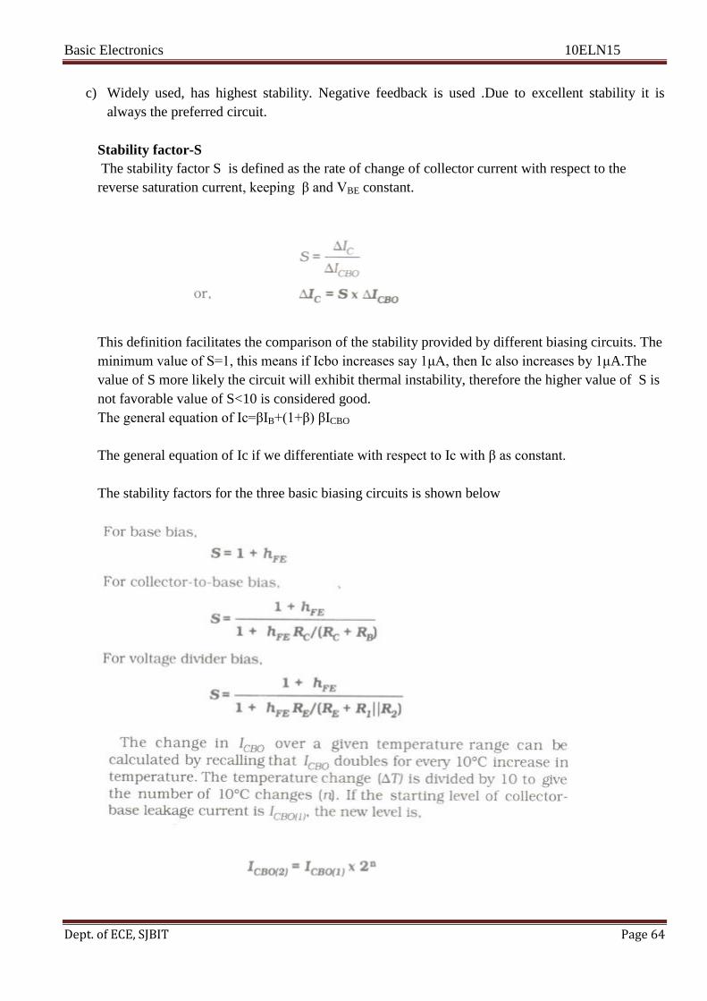
Basic Electronics 10ELN15
Dept. of ECE, SJBIT Page 64
c) Widely used, has highest stability. Negative feedback is used .Due to excellent stability it is
always the preferred circuit.
Stability factor-S
The stability factor S is defined as the rate of change of collector current with respect to the
reverse saturation current, keeping β and VBE constant.
This definition facilitates the comparison of the stability provided by different biasing circuits. The
minimum value of S=1, this means if Icbo increases say 1μA, then Ic also increases by 1μA.The
value of S more likely the circuit will exhibit thermal instability, therefore the higher value of S is
not favorable value of S<10 is considered good.
The general equation of Ic=βIB+(1+β) βICBO
The general equation of Ic if we differentiate with respect to Ic with β as constant.
The stability factors for the three basic biasing circuits is shown below

Basic Electronics 10ELN15
Dept. of ECE, SJBIT Page 65

Basic Electronics 10ELN15
Dept. of ECE, SJBIT Page 66
UNIT 4:OTHER DEVICES
4.1 Silicon Controlled Rectifier (SCR)
a) Introduction: The SCR is a rectifier constructed of silicon material with a third terminal for control
purposes. Silicon is chosen because of its high temperature and power capabilities. The current to the
control element, called the gate, determines the anode to cathode voltage at which the device commences
to conduct. The gate bias may thus either keep the device off or it may allow conduction to start.
b) Principle of Operation: As shown in Fig. 4.1(a) the SCR is a 4-1ayer device, consisting of P-type and
N-type semiconductor materials, situated alternately. The layers are called PI' N 1 ' P2 and N2' There are
three junctions : J 1 ' J2 and J3 and three terminals - anode (A), cathode (K) and gate (G).
A detailed examination of the basic operation of the SCR is effected by imagining the splitting up of
layers N1 and P2 into N1_1, N1•Z' PZ-1 and P2-2, as shown in Fig.4.1(b).

Basic Electronics 10ELN15
Dept. of ECE, SJBIT Page 67
The situation is unchanged as N1_1 is connected to NI_2 ' and P 2-1 is connectedtoP2_2' So, now we can
consider PI ' N1_1 and P2-1 as a P-N-P transistor and NI_2, P2-2 and N2 as an N-P-N transistor. The
transistor block diagram of Fig. 4.1 (b) can now be replaced by the equivalent circuit of Fig.4.2. It is
apparent that T2 collector is connected to T1 base, and the T1 collector to the T2 base. The T1 emitter is
the SCR anode terminal, and T2 emitter is the cathode and the gate is the junction of the T1 collector and
T2 base.
If a positive voltage is applied to the anode (A) and a negative voltage to the cathode (K), the SCR is
forward biased. When there is no connection given to the gate, small leakage currents flow, and both the
transistors remain cut-off. Such leakage currents are due to the junction 12 being reverse biased. When
A is positive and K is negative (as shown in Fig. 4.4).
If a negative gate-cathode voltage is applied, .the- T2 base emitter junction is reverse-biased, and there is
a flow of only small leakage currents, keeping both the transistors off.
Next, if a positive gate-cathode voltage is applied, as in Fig. 4.5, it forward biases the T2 base emitter
junction and results in the flow of base current /82'consequently producing collector current Ic2. As Ic2
and 1B1 are one and the same, T1 also switches on and Ic1 flows, providing base current 1B2' Each
collector current provides much more base current than is needed by the transistors, and even when the
gate current 1G is cut-off, the transistors remain on, conducting heavily with just a small SCR anode to
cathode drop. The phenomenon of the SCR remaining on even after the removal of its triggering current
is called latching.

Basic Electronics 10ELN15
Dept. of ECE, SJBIT Page 68
A short pulse of gate current is sufficient to switch on the SCR. Once switched on, the gate has no
further control and the device remains on until the anode-cathode voltage is reduced to near zero. If the
anode to cathode voltage is made sufficiently large, the SCR can be triggered on even though the gate is
open-circuited. Also, referring back to the earlier Fig. 4.1 (a), where a positive voltage is applied to
anode A and a negative voltage to cathode K, junctions 11 and J3 are forward biased while Jz is reverse
biased. When VF is made large enough, Jz will break down due to avalanche effect. Collector currents
flowing each of the transistors T1 and T2, Each collector current again feeds the base current and both
the transistors are switched on.
4.2 SCR Characteristics and Parameters (Fig. 4.6)
We shall first deal with the reverse characteristics.

Basic Electronics 10ELN15
Dept. of ECE, SJBIT Page 69
If a negative voltage is applied to anode A and a positive voltage is applied to cathode K, to the SCR of
Fig. 4.1 (a), the junction J2 is forward biased, while the junction J) and J3 are reverse biased. When the
reverse voltage -VAK is small, a small leakage current (of about 80 to 100 microamperes) flows, which
is called the reverse blocking current. If the reverse voltage is now increased, IRX (Reverse Blocking
Current) practically remains constant until -VAK becomes large enough to cause JI and J3 to break down
in the Zener or Avalanche mode. As is indicated in Fig. 4.6 the reverse current increases very rapidly
when the reverse breakdown voltage is reached and if I is not limited, the SCR could be damaged or
destroyed. The region of the reverse characteristics before reverse breakdown is called Reverse Blocking
Region.
4.2.1 Pulse Control of an SCR
The pulse control circuit of an SCR is given in Fig. 4.7(a). If the SCR had been an ordinary rectifier, it
would have produced a half-wave rectified voltage across the load Rc However, in this case, the SCR
will no conduct even during the positive half-cycle of the input a.c. voltage unless G is given positive
voltage to forward bias its centre most junction. By applying a trigger pulse at any time during the
positive input half-cycle, the device can be fired into conduction.
The SCR continues to conduct for the remaining part of the half cycle and switches OFF the moment the
supply voltage reaches zero. The waveform across the load is a part of the positive half-cycle, which is
shaded in Fig. 4.7(b).
The load waveforms that result from the SCR being switched on at different points in the positive half-
cycle, depending on the trigger pulse, are depicted in Fig. 4.7(b).
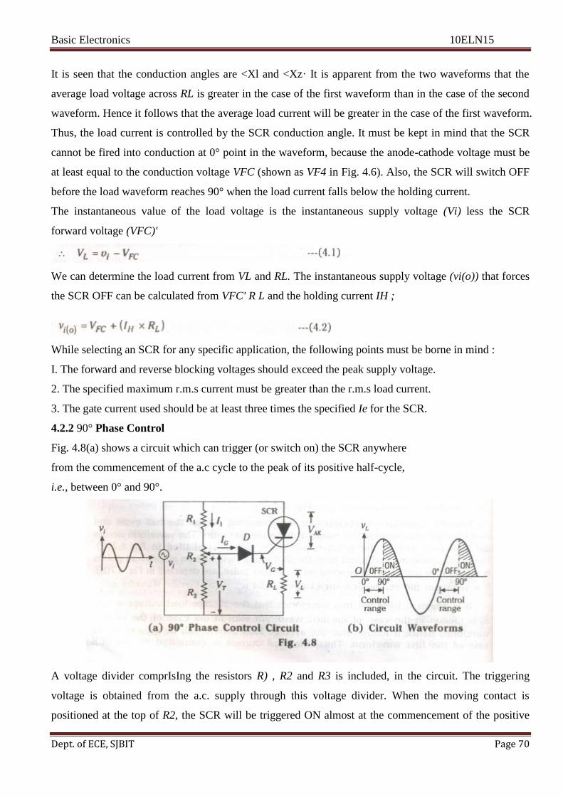
Basic Electronics 10ELN15
Dept. of ECE, SJBIT Page 70
It is seen that the conduction angles are <Xl and <Xz· It is apparent from the two waveforms that the
average load voltage across RL is greater in the case of the first waveform than in the case of the second
waveform. Hence it follows that the average load current will be greater in the case of the first waveform.
Thus, the load current is controlled by the SCR conduction angle. It must be kept in mind that the SCR
cannot be fired into conduction at 0° point in the waveform, because the anode-cathode voltage must be
at least equal to the conduction voltage VFC (shown as VF4 in Fig. 4.6). Also, the SCR will switch OFF
before the load waveform reaches 90° when the load current falls below the holding current.
The instantaneous value of the load voltage is the instantaneous supply voltage (Vi) less the SCR
forward voltage (VFC)'
We can determine the load current from VL and RL. The instantaneous supply voltage (vi(o)) that forces
the SCR OFF can be calculated from VFC' R L and the holding current IH ;
While selecting an SCR for any specific application, the following points must be borne in mind :
I. The forward and reverse blocking voltages should exceed the peak supply voltage.
2. The specified maximum r.m.s current must be greater than the r.m.s load current.
3. The gate current used should be at least three times the specified Ie for the SCR.
4.2.2 90° Phase Control
Fig. 4.8(a) shows a circuit which can trigger (or switch on) the SCR anywhere
from the commencement of the a.c cycle to the peak of its positive half-cycle,
i.e., between 0° and 90°.
A voltage divider comprIsIng the resistors R) , R2 and R3 is included, in the circuit. The triggering
voltage is obtained from the a.c. supply through this voltage divider. When the moving contact is
positioned at the top of R2, the SCR will be triggered ON almost at the commencement of the positive

Basic Electronics 10ELN15
Dept. of ECE, SJBIT Page 71
half-cycle of the a.c. input. On the other hand, if the moving contact is set at the bottom of R2, the SCR
may not switch ON until the peak of the positive half-cycle. In between these two extremes, the SCR can
be triggered ON somewhere between the zero level and the peak of the positive half-cycle, i.e., between
00 and 90°. If the triggering voltage Vr is not large enough even at the peak of the positive half-cycle
(i.e., at 90°), then the SCR will not trigger ON at all because Vr is at its maximum value at the peak of
the a.c voltage source and falls OFF past the peak. The purpose of the diode D is to protect the SCR gate
from negative voltage during the negative input half-cycle. The circuit is so designed that the voltage
divider current I) is much greater than the SCR gate current IG' The instantaneous triggering voltage at
switch ON is
The above method is also known as the amplitude firing of an SCR.
4.2.3 180 Phase Control
The circuit of Fig. 4.9 can trigger the SCR from 0° to 180° of the a.c input waveform. A second diode
Dz is incorporated in the circuit. We shall start our analysis with the negative half cycle. During the
negative half-cycle of the input, C is charged immediately (with the polarity as shown)
to the peak of the input voltage because D2 is forward-biased. When the peak of the negative half-cycle
passes over, D2 becomes reverse biased because its anode (connected to C) becomes more negative than
its cathode (connected to the supply). Hence, C starts to discharge through R. Depending on the time
constant (= CR), C may almost be completely discharged at the commencement of the oncoming positive
half-cycle or may retain partial charge until almost 1800 of the positive half-cycle has passed. So long as
C remains negatively charged, D1 is reverse-biased and the gate cannot become positive to trigger the
SCR into conduction. Hence R can be adjusted to trigger the SCR into conduction anywhere between 00
and 1800 of the input a.c cycle.

Basic Electronics 10ELN15
Dept. of ECE, SJBIT Page 72
4.3 More SCR Applications
4.3.1 SCR Circuit Stability
The stability of an SCR circuit depends upon its correct operation; the device should switch ON and
OFF at the desired instants. However, false triggering can be produced by noise voltages at the gate,
transient voltages at the anode or by rapidly changing voltages at the anode (known as dv/dt triggering).
Gate noise voltages could be large enough to forward bias the gate-cathode junction, resulting in false
triggering. Anode voltage transients, which could 'be due to other devices connected to the same a.c
source and/or due to high speed switching, could exceed the SCR breakover voltage, and thus trigger the
device into conduction. The dv/dt effect takes place when the anode voltage changes instantaneously,
such as when the supply is switched ON at its peak voltage level.
The SCR capacitance charges rapidly, and the charging current is enough to trigger the device.
Noise voltages at the gate can be restricted by using short gate connecting leads, and by connecting a
gate bias resistor RG (see Fig. 4.10 (a)). This should be kept as near as possible to the SCR gate-
cathode >terminals, because noise could be picked up by the conductors connected between RG and the
device; such noise could cause false triggering.
Noise could be effectively countered by biasing the gate negative with respect to the cathode. Capacitor
C in Fig. 4.10 (b) could be used to short circuit gate noise voltages. C also operates along with the
anode-gate capacitance as a voltage divider that limits the possibility of dv/dt triggering.
4.3.2 Zero Point Triggering
Th eNeed: If the SCR is fired into conduction while the instantaneous level of the supply voltage is more
than zero, surge currents are generated which cause· electromagnetic interference (EMf). This EM! can
adversely affect the operation of other nearby circuits and equipment, and the switching transients can
interfere with the proper control of the SCR. Hence the necessity is felt of designing circuits

Basic Electronics 10ELN15
Dept. of ECE, SJBIT Page 73
Which ensure that the SCR is triggered ON at the instant the a.c supply is crossing The zero voltage
point from the negative half-cycle to the positive half-cycle. This is known as zero-point triggering and
it effectively eliminates the EMf and the switching transients.
Fig. 4.12 shows the Zero point triggering circuit.
Two SCRs are connected in an inverse-parallel configuration. SCRI has an RC triggering circuit
comprising C1 and RI ' while SCR2 has another RC triggering circuit made up of C2 and R2. When
switch 5 I is closed, there is no current to its gate; hence it is OFF. SCR2 too remains OFF as SCR is
uncharged.
4.3.3 Crowbar Circuit
If anything happens inside a power supply to cause its output voltage to go excessively high, the results
can be devastating, because some loads such as expensive digital ICs cannot withstand too much supply
voltage without being destroyed. One of the most important applications of the SCR is to protect delicate
and expensive loads against over voltages from a power supply. Fig. 4.13 shows a power supply of Vcc
applied to a protected load. Under normal conditions, Vcc is less than the breakdown voltage of the
Zener diode.

Basic Electronics 10ELN15
Dept. of ECE, SJBIT Page 74
Hence the diode does not conduct and there is no current through the gate bias register R; in this case
there is no voltage across R. The gate voltage Va remains equal to zero and SCR remains open. The load
receives a voltage of Vcc and all is well.
Now, if the supply voltage increases for any reason and exceeds Vz' the zener diode breaks down, current
flows through R and a voltage appears across R. If this voltage is greater than the gate trigger voltage of
the SCR, the SCR fires and becomes a closed latch; the power supply is shorted by the SCR. This action
is similar to throwing a crowbar across the load terminals. Because the SCR turnon is very fast (I Ils for
a 2N444I), the load is quickly protected against the damaging effects of a large overvoltage. The
overvoltage that fires the SCR is
Crowbarring, though a drastic form of protection, is necessary with many digital ICs because they can't
take much overvoltage. Rather than destroy expensive ICs, therefore, we can use an SCR crowbar to
short the load terminals at the first sign of overvoltage. With an SCR crowbar, a fuse or current limiter is
needed to prevent damage to the power supply.
4.3.4 Heater Control Circuit
The SCR heater control circuit is shown in Fig. 4.14.
The circuit of Fig.4.14 uses a temperature sensitive control element (Rz). When the temperature rises, the
resistance of Rz decreases; when the temperature falls, the resistance of Rz increases. Diode D keeps the
capacitor C charged to the supply voltage peak. C, along with resistor R I ' functions as a constant
current source for R2.
When the temperature rises to the predetermined level, the resistance of R2 decreases, dropping VG to a
level which keeps the SCR from triggering; consequently the power is turned OFF to the' heater load.
When the temperature drops to a specified level, the resistance of Rz increases, causing VG to increase to
the SCR triggering level, as a result of which the power is turned ON to the heater load. The rectifier D2

Basic Electronics 10ELN15
Dept. of ECE, SJBIT Page 75
could be inserted in the circuit, as shown, to pass the negative half cycle of the supply waveform to the
heater
load.
4.4 Unijunction Transistor (UJT)
Introduction
Though the Unijunction Transistor is a 3-terminal device, it is quite different from the bipolar and field
effect transistors as far as operation is concerned. The device input, called the Emitter, has a resistance
which rapidly decreases when the input voltage reaches a certain level. This is called a
negative ."esistance characteristic, and it is this characteristic which makes the UJT useful in a
numberof applications.
UJT Operation
The basic construction, the symbol and the equivalent circuit of a WT are
given in Figs. 4.15 (a), (b) and (c).
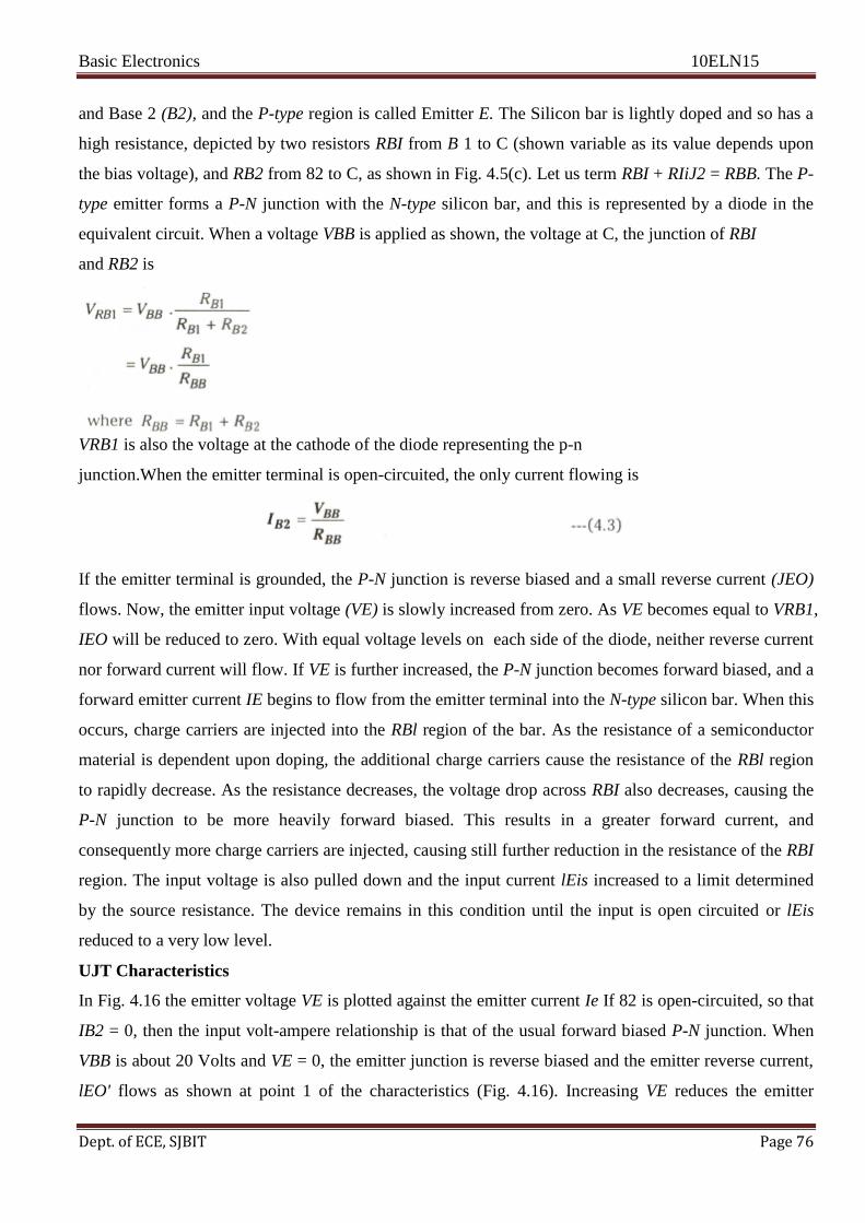
Basic Electronics 10ELN15
Dept. of ECE, SJBIT Page 76
and Base 2 (B2), and the P-type region is called Emitter E. The Silicon bar is lightly doped and so has a
high resistance, depicted by two resistors RBI from B 1 to C (shown variable as its value depends upon
the bias voltage), and RB2 from 82 to C, as shown in Fig. 4.5(c). Let us term RBI + RIiJ2 = RBB. The P-
type emitter forms a P-N junction with the N-type silicon bar, and this is represented by a diode in the
equivalent circuit. When a voltage VBB is applied as shown, the voltage at C, the junction of RBI
and RB2 is
VRB1 is also the voltage at the cathode of the diode representing the p-n
junction.When the emitter terminal is open-circuited, the only current flowing is
If the emitter terminal is grounded, the P-N junction is reverse biased and a small reverse current (JEO)
flows. Now, the emitter input voltage (VE) is slowly increased from zero. As VE becomes equal to VRB1,
IEO will be reduced to zero. With equal voltage levels on each side of the diode, neither reverse current
nor forward current will flow. If VE is further increased, the P-N junction becomes forward biased, and a
forward emitter current IE begins to flow from the emitter terminal into the N-type silicon bar. When this
occurs, charge carriers are injected into the RBl region of the bar. As the resistance of a semiconductor
material is dependent upon doping, the additional charge carriers cause the resistance of the RBl region
to rapidly decrease. As the resistance decreases, the voltage drop across RBI also decreases, causing the
P-N junction to be more heavily forward biased. This results in a greater forward current, and
consequently more charge carriers are injected, causing still further reduction in the resistance of the RBI
region. The input voltage is also pulled down and the input current lEis increased to a limit determined
by the source resistance. The device remains in this condition until the input is open circuited or lEis
reduced to a very low level.
UJT Characteristics
In Fig. 4.16 the emitter voltage VE is plotted against the emitter current Ie If 82 is open-circuited, so that
IB2 = 0, then the input volt-ampere relationship is that of the usual forward biased P-N junction. When
VBB is about 20 Volts and VE = 0, the emitter junction is reverse biased and the emitter reverse current,
lEO' flows as shown at point 1 of the characteristics (Fig. 4.16). Increasing VE reduces the emitter

Basic Electronics 10ELN15
Dept. of ECE, SJBIT Page 77
junction reverse bias. When VE = VRB1 , (refer Fig.4.15(c)), there is no reverse or forward bias and IE =
0. This happens to take place at the value of VE= 12 volts as given by point 2. Increasing beyond this
point begins to forward bias the emitter junction, reaching a peak point V . At this peak point, the
junction p is a little forward biased and a very small forward emitter current flows, which is called the
Peak Current I . Upto this point, the UJT is said to be operating in the p cut-off region. After that,
increase of VE results in a sudden increase in emitter current IE and VE falls to the Valley Voltage VV'
At this point, IE equals the Valley Current Iv' The region of the characteristics between Peak Point and
Valley Point is the Negative Resistance Region of the characteristics. A further increase incurrent causes
the device to enter the saturation region.
When Vss is reduced below 20 Volts, VE is also reduced and the UJT will switch on at a lower value of
voltage. Thus, using the different values of VSS'a family of V E -IE characteristics for a given UJT can
be plotted as shown.
UJT Parameters
1. Interbase Resistance (RBB) :
This is equal to the sum of RBI and RS2' i.e., Rss = RBI + RB2 when theemitter is open circuited (IE = 0).
The value of Rss' along with themaximum power dissipation PD(max)' determine the maximum value of
Vss' With IE = 0,
As in the case of other devices PD(max) of the UJT has to be to derated for 6. 11

Basic Electronics 10ELN15
Dept. of ECE, SJBIT Page 78
higher temperatures.
2. Intrinsic Standoff Ratio (11) The intrinsic stand off ratio is
The peak-point voltage is calculated from 11. the supply voltage and the diode
voltage drop;
3. Emitter Saturation Voltage (VE(sat)): This is the emitter voltage when the UJT is operating in the
saturation region of its characteristics (refer to Fig. 4.16). As it is affected by the emitter current and
supply voltage, VE(sat) is specified for given IE and VBB levels.
4. Peak Point Emitter Current (,pI ): This current is the minimum emitter
current, corresponding to the start of the negative resistance region as shown
in Fig.4.16. The UJT will be triggered into conduction only of IE> I .
The maximum emitter source resistance is
5. Valley Point Current (/)v: This is of significance in some circuits, as it is the maximum current in the
negative resistance region of the characteristics. If the emitter voltage source resistance is so low that IE
is equal to or greater than Iv, the UJT will remain ON when triggered and will not switch OFF. Hence,
the minimum emitter voltage source resistance is
4.4.1Areas of Application of UJT
The negative resistance characteristics of the UJT makes it useful in timing & oscillator circuits
(especially as a Relaxation Oscillator, whose frequency may be varied to provide an excellent method of
motor speed control).
One rather common application of the UJT is the triggering of other devices like the SCR and thyristors.
3. It is used in pulse and voltage sending circuits.
4. It finds application in sawtooth generator and pulse generator.
5. It is used in switching applications.
6. It is used in Over-voltage Detector circuits.

Basic Electronics 10ELN15
Dept. of ECE, SJBIT Page 79
4.4.2 UJT Relaxation Oscillator
The Relaxation oscillator circuit is given in Fig. 4.17.
The circuit of a UJT Relaxation Oscillator is given in Fig. 4.17(a). Capacitor e is charged through RE.
When the capacitor voltage Vc reaches the value Vp in time ts' the UJT fires and rapidly discharges e till
the voltage falls to the minimum value Vv. The device then cuts OFF and the capacitor starts charging
again.
The cycle is repeated continuously, generating a sawtooth waveform across e, as shown in Fig.4.17(b).
The inclusion of external resistances R1 and R4 provide spike waveforms. When the UJT fires, the
sudden surge of current through B I causes a drop across R4 which produces positive-going voltage
spikes, and at the same time negative - going voltage spikes are produced across R I (both are shown in
Fig.4.17(b). Condition for Turn-ON and Turn-OFF For satisfactory operation of the above oscillator, the
following two conditions for the turn-on anrl 11!rn-off of the UJT must be met. To ensure turn-on, RE
must not limit /E at peak point to a value less than /p' It means that
To ensure turn-off of the UJT at the valley point, RE must be large enough to permit IE (at valley point)
to decrease below the specified value of Iv. In other words, drop across RE at valley point must be less
than Iv RE. Hence, condition for turn-off is

Basic Electronics 10ELN15
Dept. of ECE, SJBIT Page 80
Hence, for reliable turn-on and turn-off of the UJT, RE must be in the range
The charging time constant of the capacitor for voltage VBB is T = CRE, whereas the discharging time
constant is Td = CR8l. The time required to charge upto V (called ramp rise time) is
Similarly, time required by the capacitor to discharge from Vp 10 Vv is
The frequency of oscillation is given by
4.4.3 UJT Control of an SCR
Unijunction transistors are often used in SCR control circuits. Referring to the circuit of Fig. 4.18(a), the
diode D, resistor Rl and the zener diode Z provide a low-voltage d.c. supply to the UJT circuit, obtained
from the positive half-cycle of the a.c.supply. The function of the diode D is to pass only the positive
half cycle and blocking the negative half-cycle of the a.c .supply. The capacitor C is charged through
resistor R2 to the UJT firing voltage (The rising capacitor waveform ab of Fig.4.18(b), and the SCR is
triggered into conductionby voltage spike produced across the resistor R3.

Basic Electronics 10ELN15
Dept. of ECE, SJBIT Page 81
By adjusting R2, the charging rate of C and the UJT firing time can be chosen. The falling part of the
capacitor waveform, bc, shows the capacitor discharge.
From the waveforms of Fig. 4.18, it is obvious that 1800 of SCR phase control is possible.
4.5 Field Effect Transistor (FET)
Introduction :
A field effect transistor (FET) is a semiconductor device. While a BJT is a current-controlled device, a
FET is a voltage-controlled device. A FET requires very little current, hence its input resistance is very
high, which is its most important advantage over a BJT. There are two types of FET : the Junction FET
and the Metal Oxide Field Effect Transistor (MOSFET). However, we shall discuss only the Junction
Field Effect Transistors (JFET), which are further subdivided into N-channel and P-channel devices.
4.5.1 Junction Field Effect Transistors
i) N-channel JFET
For fabricating an N-channel JFET, first a narrow bar of N-type semiconductor
material, called the channel, is taken and then two smaller P-type pieces
(the gates) are diffused on opposite sides of its middle part (Fig.4.19(a».

Basic Electronics 10ELN15
Dept. of ECE, SJBIT Page 82
The ends of the channel are called the Drain (D) and the Source (5). The two pieces of P-type material
are interconnected and a single lead is brought out which is called the gate terminal.
When the gate is left open, a drain-source voltage (VD) is applied, positive at the drain and negative at
the source, so that a drain current (ID) flows as shown in Fig. 4.19(a). When a gate-source voltage (Vas)
is applied, with the gate negative with respect to the source (Fig. 4.19(b)), the gate-channel PN-junctions
are reverse biased.
The block diagram of a P-channel JFET is shown in Fig. 4.20. In this case, the channel is a narrow bar of
P-type semiconductor material, to which two N-type pieces (the gates) are diffused. The drain-source
voltage (VD) is applied, negative to the drain, positive to the source, as shown and the drain current ID
flows from the source to the drain.
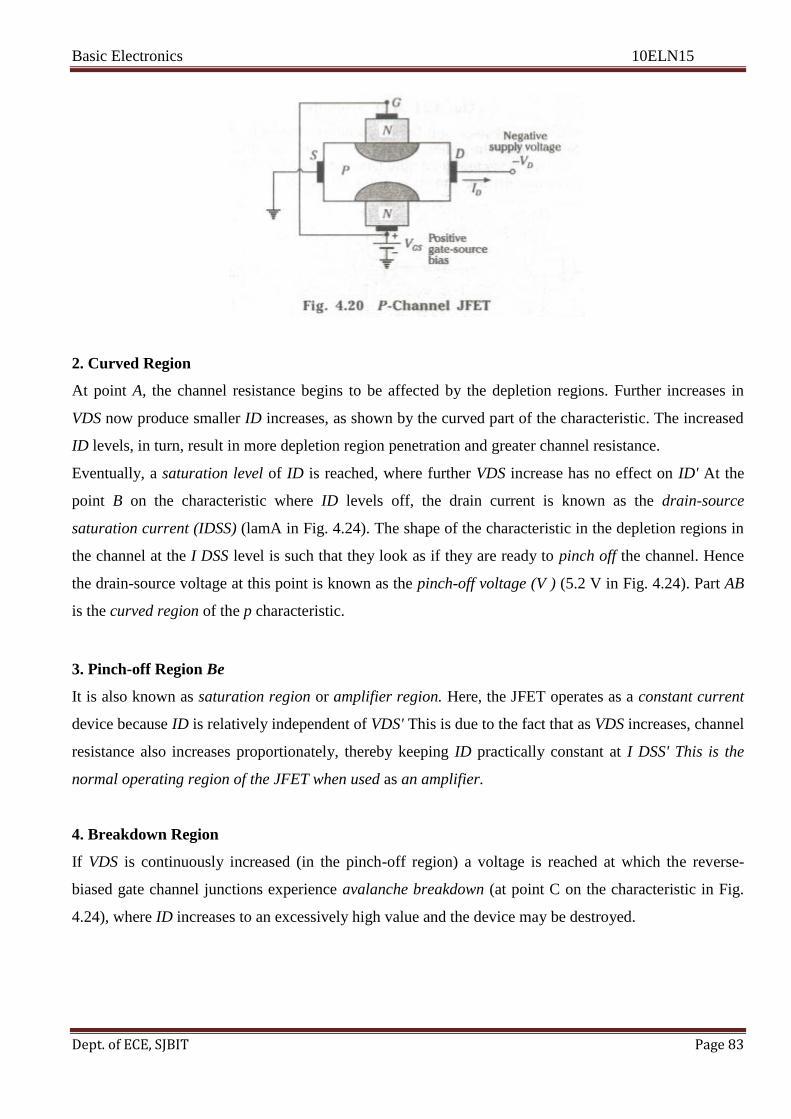
Basic Electronics 10ELN15
Dept. of ECE, SJBIT Page 83
2. Curved Region
At point A, the channel resistance begins to be affected by the depletion regions. Further increases in
VDS now produce smaller ID increases, as shown by the curved part of the characteristic. The increased
ID levels, in turn, result in more depletion region penetration and greater channel resistance.
Eventually, a saturation level of ID is reached, where further VDS increase has no effect on ID' At the
point B on the characteristic where ID levels off, the drain current is known as the drain-source
saturation current (IDSS) (lamA in Fig. 4.24). The shape of the characteristic in the depletion regions in
the channel at the I DSS level is such that they look as if they are ready to pinch off the channel. Hence
the drain-source voltage at this point is known as the pinch-off voltage (V ) (5.2 V in Fig. 4.24). Part AB
is the curved region of the p characteristic.
3. Pinch-off Region Be
It is also known as saturation region or amplifier region. Here, the JFET operates as a constant current
device because ID is relatively independent of VDS' This is due to the fact that as VDS increases, channel
resistance also increases proportionately, thereby keeping ID practically constant at I DSS' This is the
normal operating region of the JFET when used as an amplifier.
4. Breakdown Region
If VDS is continuously increased (in the pinch-off region) a voltage is reached at which the reverse-
biased gate channel junctions experience avalanche breakdown (at point C on the characteristic in Fig.
4.24), where ID increases to an excessively high value and the device may be destroyed.

Basic Electronics 10ELN15
Dept. of ECE, SJBIT Page 84

Basic Electronics 10ELN15
Dept. of ECE, SJBIT Page 85
Example 4.1
Plot the ID/ VDS characteristics for an N-channel JFET from the following table of current and voltage
levels obtained with VGS = O. Determine IDSS and Vp from the characteristics.
Transfer Characteristics (Fig. 4.27)
The circuit of Fig. 4.23 is used to experimentally obtain the various values for plotting the transfer
characteristic of a given JFET. The drain source voltage is held constant, VGS is adjusted in steps using
the variable resistor R, and the corresponding levels of VGS and ID are recorded. From the characteristic
it is seen that, as -V GS is increased, ID is successively reduced from IDSS at VGS = 0, to ID = ° at Ves =
-Vp' The transfer characteristic of the JFET can be derived from the drain characteristics. A line AB is
drawn vertically on the drain characteristic (Fig. 4.25), signifying a constant VDS level. The
corresponding IDand VGS values are recorded and then the transfer characteristic is drawn. This process
is shown in Fig. 4.25.

Basic Electronics 10ELN15
Dept. of ECE, SJBIT Page 86
P·channel JFET Characteristics
Fig. 4.28 shows a circuit for obtaining the characteristics of a P-channel JFET.
The drain terminal is negative with respect to the base, and the gate terminal is positive with respect to
the source. For plotting the drain characteristic, VGS is kept constant and -VDS is increased in
convenient steps, as shown in Fig. 4.29, The JFET transfer characteristics too have been shown
alongside. It may be noted that these characteristics resemble the characteristics of an N-channel JFET,
except that the voltage polarities are the opposite.

Basic Electronics 10ELN15
Dept. of ECE, SJBIT Page 87
Referring to the P-channel JFET characteristics of Fig. 4.29, when VGS = 0, IDSS = 12 mA. Now, when
more positive value of VGS are applied, the more is the level of ID reduced till it is cut off at Vp = +4.5
V. If VGS = -0.5 V is used, higher levels of ID are obtained than when V GS = O. As it was in the case
of the N-channel JFET, forward bias at the gate-channel junction should be avoided, Hence, as a rule,
negative values of VGS are avoided with a P-channel JFET. The transfer characteristic of the P-channel
JFET are obtained experimentally, Alternatively, it can be derived from the drain characteristic, as
shown in Fig. 4.29, just as it was done in the case of an N-channel JFET.
Example 4.2 The following table of plots of ID and VDS for a FET were obtained with
VGS = O. Draw the drain characteristic and find the values of IDSS and Vp-

Basic Electronics 10ELN15
Dept. of ECE, SJBIT Page 88
IDSS = 5.5 mA and Vp = 6.25 V from the drain characteristic drawn in Fig. 4.30.

Basic Electronics 10ELN15
Dept. of ECE, SJBIT Page 89
UNIT 5:AMPLIFIERS & OSCILLATORS
Amplifier is an electronic circuit which is used to amplify ac or dc signals, resulting in increasing
the amplitude from low level to high level. Active devices such as transistor, op-amp, FET,etc. are used
to do the amplification. The amplifier is versatile and essential device particularly in communication
systems where signals are transmitted over long distances and are weak when received, requiring
amplification.
Usually the gain, defined as the ratio of output voltage to the input voltage is very high, and requires
faithful reproduction of input at the output. In the above case the amplifier is referred to as voltage
amplifier. Similarly, if the current, or power, of the signal need to be amplified, then accordingly, it is
called current or power amplifier.
Generally, a portion of the output is fed back to the input for stabilization. The feed back can be used to
aid or oppose the input. If the output feedback at the input opposes the input or applied in phase
opposition with the input then the amplifier is called negative feedback amplifier. If the output feedback
at the input aid the input or applied in phase with the input then the amplifier is called positive feedback
amplifier. The positive feedback is used for oscillators (a circuit produces oscillation using dc supply).
The amplifiers with negative feedback is discussed below.
Classification of the amplifiers:
Amplifiers are classified according to frequency of operation, mode of operation, biasing condition,
configuration used, methods of feed back, etc. as follows:
1.Based on its input:
a. Small signal amplifiers.
b. Large signal amplifiers
2.Based on its output;
a. Voltage amplifiers
b. Current amplifiers
c. Power amplifiers
3 Based on its frequency;
a. Audio frequency amplifiers
b. Radio frequency amplifiers
c. Inter-mediate frequency amplifiers.
d. Ultra high frequency amplifiers.
4.Based on biasing conditions:
a.Class ‗A‘amplifiers
b.Class ‗B‘amplifiers
c.Class ‗C‘amplifiers
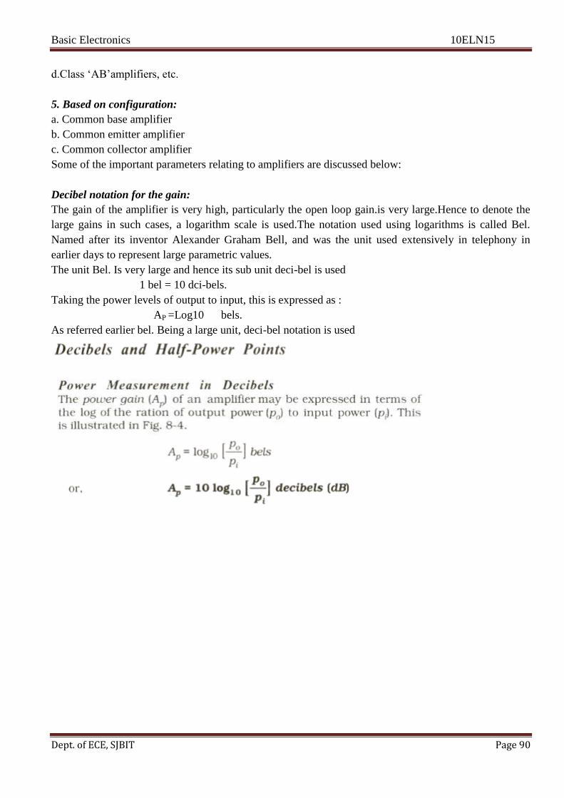
Basic Electronics 10ELN15
Dept. of ECE, SJBIT Page 90
d.Class ‗AB‘amplifiers, etc.
5. Based on configuration:
a. Common base amplifier
b. Common emitter amplifier
c. Common collector amplifier
Some of the important parameters relating to amplifiers are discussed below:
Decibel notation for the gain:
The gain of the amplifier is very high, particularly the open loop gain.is very large.Hence to denote the
large gains in such cases, a logarithm scale is used.The notation used using logarithms is called Bel.
Named after its inventor Alexander Graham Bell, and was the unit used extensively in telephony in
earlier days to represent large parametric values.
The unit Bel. Is very large and hence its sub unit deci-bel is used
1 bel = 10 dci-bels.
Taking the power levels of output to input, this is expressed as :
AP =Log10 bels.
As referred earlier bel. Being a large unit, deci-bel notation is used

Basic Electronics 10ELN15
Dept. of ECE, SJBIT Page 91
Fig : Amplifier power gain is measured in decibels(db)
Advantages of representing in db.
We have seen that the overall gain of the multistage amplifier is the product of individual gains.Instead
of multiplying the individual gains and representing,the log scale permits us to add individual gains in
db.The deci-bel notation allows us to represent a very small like 10-6
Volts or a very large values like
10+6
using deci-bels.
The hearing effects perceived by the ear is logarithmic hence use of db. notation will become very
usefull while representing figures in audio frequency amplifiers.
Oscillators
An oscillator is a circuit that produces an output waveform with only a dc power supply input.
The range of frequencies required by electronic devices may range from a few hertz into the megahertz
region, and these signals are generally produced by oscillators. In this chapter we focus on sine-wave
oscillators.
Oscillators are circuits that produce an output waveform without an external signal source. The key to
oscillator operation is positive feedback. A positive feedback network produces a feedback voltage ( )
that is in phase with the input signal ( ) as shown in Figure 1. The amplifier shown in the figure
produces a 180° voltage phase shift, and the feedback network introduces another 180° voltage shift.
This results in a combined 360° voltage phase shift, which is the same as a 0° shift. Therefore, is in
phase with . (Positive feedback can also be achieved by using an amplifier and a feedback network
that both generate a 0° phase shift.)
Figure 5.1 illustrates the basic principle of how the oscillator produces an output waveform without any
input signal. In Figure 5.1 , the switch is momentarily closed, applying an input signal to the circuit.

Basic Electronics 10ELN15
Dept. of ECE, SJBIT Page 92
This results in a signal at the output from the amplifier, a portion of which is fed back to the input by the
feedback network.
In Figure 5.1(b) -, the switch is now open, but the circuit continues to oscillate because the feedback
network is supplying the input to the amplifier. The feedback network delivers an input to the amplifier,
which in turn generates an input for the feedback network. This circuit action is referred to as
regenerative feedback and is the basis for all oscillators.
. FIGURE 5.1 Regenerative feedback
There is one other requirement for oscillator operation. The circuit must fulfill a condition referred to as
the Barkhausen criterion.
We know that the active component in a feedback amplifier produces a voltage gain (Av ) while the
feedback network introduces a loss or attenuation (αv). In order for an oscillator to work properly, the
following relationship must be met:
Av αv = 1 Av
This relationship is called the Barkhausen criterion. If this criterion is not met, one of the following
occurs:
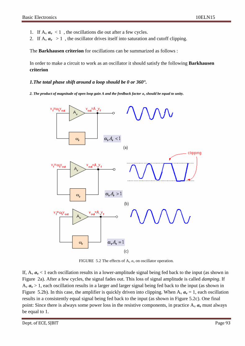
Basic Electronics 10ELN15
Dept. of ECE, SJBIT Page 93
1. If Av αv < 1 , the oscillations die out after a few cycles.
2. If Av αv > 1 , the oscillator drives itself into saturation and cutoff clipping.
The Barkhausen criterion for oscillations can be summarized as follows :
In order to make a circuit to work as an oscillator it should satisfy the following Barkhausen
criterion
1.The total phase shift around a loop should be 0 or 360°.
2. The product of magnitude of open loop gain A and the feedback factor αv should be equal to unity.
FIGURE 5.2 The effects of Av αv on oscillator operation.
If, Av αv < 1 each oscillation results in a lower-amplitude signal being fed back to the input (as shown in
Figure 2a). After a few cycles, the signal fades out. This loss of signal amplitude is called damping. If
Av αv > 1, each oscillation results in a larger and larger signal being fed back to the input (as shown in
Figure 5.2b). In this case, the amplifier is quickly driven into clipping. When Av αv = 1, each oscillation
results in a consistently equal signal being fed back to the input (as shown in Figure 5.2c). One final
point: Since there is always some power loss in the resistive components, in practice Av αv must always
be equal to 1.

Basic Electronics 10ELN15
Dept. of ECE, SJBIT Page 94
Positive feedback Amplifier-Oscillator
1. A transistor amplifier with proper +ve feedback can act as an oscillator.
S
Vout
Vin Vf
t t t
2. The circuit needs only a quick trigger signal to start the oscillations. Once the oscillations have
started, no external signal source is necessary.
3. In order to get continuous undamped output from the circuit, the following condition must be met;
Av αv =1
where AV = voltage gain of amplifier without feedback.
αv = feedback fraction.
This relation is also called Barkhausen criterion
Essentials of Transistor Oscillator
Fig. below shows the block diagram of an oscillator. Its essential components are:
1. Tank Circuit: It consists of inductance coil (L) connected in parallel with capacitor(C ). The
frequency of oscillations in the circuit depends upon the values of inductance of the coil and
capacitance of the capacitor.
2. Transistor Amplifier: The transistor amplifier receives d.c. power from the battery and changes
it into a.c. power for supplying to the tank circuit. The oscillations occurring in the tank circuit
are applied to the input the transistor amplifier. The output of the transistor can be supplied to the
tank circuit to meet the losses.
3. Feedback circuit: The feedback circuit supplies a part of collector energy to the tank circuit in
correct phase to aid the oscillations. I e. To provide positive feedback.
Amplifier
Feedback
network

Basic Electronics 10ELN15
Dept. of ECE, SJBIT Page 95
Fig. 5.3 Block diagram of Transistor Oscillator
Types of Transistor Oscillators
1. Colpitt’s Oscillator
2. Hartley Oscillator
3. Phase Shift Oscillator
4. Crystal Oscillator
Colpitt’s Oscillator
The Colpitt‘s and Hartly oscillators depends for their operation on the principle of tank circuit explained
below.
Oscillatory circuit using LC tank circuit :
A circuit, which produces electrical oscillations of any desired frequency, is known as an oscillatory
circuit or tank circuit.
A simple oscillatory circuit consists of a capacitor C and inductance coil L in parallel as shown in figure
below. This electrical system can produce electrical oscillations of frequency determined by the values
of L and C.
― An electronic device that generates sinusoidal oscillations of desired frequency is known as sinusoidal
oscillator‖
S
++ ++
L C _ _ _ _
Transistor
Amplifier
Feedback
circuit

Basic Electronics 10ELN15
Dept. of ECE, SJBIT Page 96
Fig.1 Fig. 2
_ _
+ +
Fig. 5.4 Fig. 5.5
Circuit operations- Assume capacitor is charged from a d. c. source with a polarity as shown in
fig.
When switch S is closed as shown in fig2, the capacitor will discharges through inductance, and
the electron flow will be in the direction indicated by the arrow. This current flow sets up
magnetic field around the coil. Due to the inductive effect, the current builds up slowly towards a
maximum value. The circuit current will be maximum when the capacitor is fully discharged.
Hence the electrostatic energy across the capacitor is completely converted into magnetic field
energy, around the coil.
Once the capacitor is discharged, the magnetic field will begin to collapse and produce a counter
emf. According to Lenz‘s law the counter emf will keep the current flowing in the same direction.
The result is that the capacitor is now charged with opposite polarity making upper plate of
capacitor –ve and lower plate +ve as shown in fig. 3.
After the collapsing field has recharged the capacitor, the capacitor now begins to discharge and
current now flows in the opposite direction as shown in fig.4.
The sequence of charge and discharge results in alternating motion of electrons or an oscillating
current. The energy is alternately stored in the electric field of the capacitor C and the magnetic
field of the inductance coil L . This interchange of energy between L and C is repeated over and
again resulting in the production of Oscillations.
Waveform- In practical tank circuit, there are resistive and radiation losses in the coil and dielectric
losses in the capacitor. During each cycle a small part of the originally imparted energy is used up, to
overcome these losses. The result is that the amplitude of oscillating current decreases gradually and
eventually it become zero. Therefore tank circuit produces damped oscillations.
Frequency of oscillations- The expression for frequency of oscillation is given by,
LCf r
2
1 -------------------------------(1)

Basic Electronics 10ELN15
Dept. of ECE, SJBIT Page 97
Undamped Oscillations from Tank Circuit
A tank circuit produces damped oscillations. In practice we need continuous un-damped oscillations for
the successful operation of electronics equipment. In order to make the oscillations in the tank circuit un-
damped it is necessary to supply correct amount of energy to the tank circuit at the proper time intervals
to meet the losses.
The following conditions must be fulfilled;
1. The amount of energy supplied be such so as to meet the losses in the tank and the a.c. energy
removed from the circuit by the load. For example if losses in LC circuit amount ot 5 mW and
a.c. output being taken is 100 mW, then power of 105mW should be continuously supplied to the
circuit.
2. The applied energy should have the same frequency as that of the oscillations in the tank circuit.
3. The applied energy should be in phase with the oscillations set up in the tank circuit.
The Colpitts Oscillator
The Colpitts oscillator is a discrete LC oscillator that uses the tank circuit described above.A pair of
tapped capacitors and an inductor is used to produce regenerative feedback. A Colpitts oscillator is
shown in Figure -5.5. The operating frequency is determined by the tank circuit. By the formula:
T
FIG -5.5 Colpitts oscillator.
The key to understanding this circuit is knowing how the feedback circuit produces its 180° phase shift
and the other 180° is produced from the inverting action of the CE amplifier. The feedback circuit
produces a 180° voltage phase shift as follows:
1. The amplifier output voltage is developed across .
2. The feedback voltage is developed across .

Basic Electronics 10ELN15
Dept. of ECE, SJBIT Page 98
3. As each capacitor causes a 90° phase shift, the voltage at the top of (the output voltage) must
be 180° out of phase with the voltage at the bottom of (the feedback voltage).
The first two points are fairly easy to see. is between the collector and ground. This is where the
output is measured.
is between the transistor base and ground, or in other words, where the input is measured. Point three
is explained using the circuit in Fig -5.6.
FIG -5.6
Fig 5. 6 is the equivalent representation of the tank circuit in the Colpitts oscillator. Let‘s assume that the
inductor is the voltage source and it induces a current in the circuit. With the polarity shown across the
inductor, the current causes potentials to be developed across the capacitors with the polarities shown in
the figure. Note that the capacitor voltages are 180° out of phase with each other. When the polarity of
the inductor voltage reverses, the current reverses, as does the resulting polarity of the voltage across
each capacitor (keeping the capacitor voltages 180° out of phase).
The value of the feedback voltage is determined (in part) by the of the circuit. For the Colpitts
oscillator, is defined by the ratio of . By formula:
Av = XC2/X C1 or C 1/C 2
As with any oscillator, the product of A β must be slightly greater than 1. As mentioned earlier
and . Therefore:
Av = Vout/Vf = C2/C1
As with any tank circuit, this one will be affected by a load. To avoid loading effects (the circuit loses
some efficiency), the output from a Colpitts oscillator is usually transformer-coupled to the load, as .
Capacitive coupling is also acceptable so long as:
where is the total capacitance in the feedback network

Basic Electronics 10ELN15
Dept. of ECE, SJBIT Page 99
Hartley oscillator:
The Hartley oscillator is similar to the Colpitts except that it uses a pair of tapped coils instead of two
tapped capacitors. For the circuit in Fig -5.7, the output voltage is developed across and the feedback
voltage is developed across . The attenuation caused by the feedback network ( ) is found as:
= XL2/X L1 or L 2/L 1
The tank circuit, just like in the Colpitts, determines the operating frequency of the Hartley oscillator. As
the tapped inductors are in series, the sum of must be used when calculating the value of .
FIG 5.7 Hartley oscillator.
Demerits of Oscillator using Tank Circuit
1. They suffer for frequency instability and poor waveform
2. They cannot be used to generate low frequencies, since they become too-much bulky and
expensive too.
RC Phase Shift Oscillator
Fig5.8: Circuit diagram of RC phase shift Oscillator
Basic Electronics 10ELN15
Dept. of ECE, SJBIT Page 100
It consists of a conventional single transistor amplifier and a RC phase shift circuit. The RC
phase shift circuit consists of three sections R1C1, R2C2, and R3C3.At some particular frequency f0
the phase shift in each RC section is 600 so that the total phase shift produced by the RC network
is 1800. The frequency of oscillation is given by
62
1
RCfo
---------------------------(6)
When the circuit is switched ON it produces oscillations of frequency determined by equation 1.
The output EO of the amplifier is feedback to RC feedback network. This network produces a
phase shift of 1800 and the transistor gives another 180
0 shift. Thereby total phase shift of the
output signal when fed back is 3600
Merits-
1. They do not require any transformer or inductor thereby reduce the cost.
2. They are quite useful in the low frequency range where tank circuit oscillators cannot be
used.
3. They provide constant output and good frequency stability.
Demerits –
1. It is difficult to start oscillations.
2. The circuit requires a large number of components.
3. They cannot generate high frequencies and are unstable as variable frequency generators.
Crystal Oscillator
Crystal-Controlled Oscillators :
In applications where extremely stable operating frequencies are required, the oscillators that we have
studied so far come up short. They can experience variations in both frequency and amplitude for several
reasons:
If the transistor is replaced, it may have slightly different gain characteristics.
If the inductor or capacitor is changed, the operating frequency may change.
If circuit temperature changes, the resistive components will change, which can cause a change in
both frequency and amplitude.
In any system where stability is paramount, crystal-controlled oscillators are used. Crystal-controlled
oscillators use a quartz crystal to control the operating frequency.
The key to the operation of a crystal-controlled oscillator is the piezoelectric effect, which means that
the crystal vibrates at a constant rate when it is exposed to an electric field. The physical dimensions of
the crystal determine the frequency of vibration. Thus, by cutting the crystal to specific dimensions, we

Basic Electronics 10ELN15
Dept. of ECE, SJBIT Page 101
can produce crystals that have very exact frequency ratings. There are three commonly used crystals that
exhibit piezoelectric properties. They are Rochelle salt, quartz, and tourmaline. Rochelle salt has the best
piezoelectric properties but is very fragile. Tourmaline is very tough, but its vibration rate is not as
stable. Quartz crystals fall between the two extremes and are the most commonly used.
Quartz crystals are made from silicon dioxide ( ). When used in electronic components, a thin slice
of crystal is placed between two conductive plates, like those of a capacitor. Remember that its physical
dimensions determine the frequency at which the crystal vibrates.
FIG 5.9 Crystal symbol, equivalent circuit, and frequency response.
The electrical operation of the crystal is a function of its physical properties, but it can still be
represented by an equivalent circuit. Following arte the components in the equivalent circuit which
represents specific crystal characteristics:
= the capacitance of the crystal itself
= the mounting capacitance, or the capacitance between the crystal and the two conducting plates
L = the inductance of the crystal
R = the resistance of the crystal
The primary points are as follows:
1. At the crystal acts as a series resonant circuit.
2. At the crystal acts as a parallel resonant circuit.

Basic Electronics 10ELN15
Dept. of ECE, SJBIT Page 102
This means that a crystal can be used to replace either a series or a parallel resonant LC circuit. It should
also be noted that there is very little difference between and . The spacing between these frequencies
in the response curve (Figure 8) is exaggerated for illustrative purposes only.
A crystal can produce outputs at its resonant frequency and at harmonics of that resonant frequency.
This concept was introduced when we looked at tuned class C amplifiers. The resonant frequency is
often referred to as the fundamental frequency, and the harmonic frequencies as overtones. Crystals
are limited by their physical dimensions to frequencies of 10 MHz or below. If the circuit is tuned to one
of the harmonic frequencies of the crystal (overtones), then we can produce stable outputs much higher
than the 10 MHz limit of the crystal itself. This type of circuit is said to be operating in overtone mode.
A Colpitts oscillator can be modified into a crystal-controlled oscillator (CCO) as shown in Figure 9.
Note that the crystal is in series with the feedback path and is operating in series-resonant mode ( ). At
the impedance of the crystal is almost zero and allows the feedback signal to pass unhindered. As the
crystal has an extremely high Q, the circuit will only oscillate over a very narrow range of frequency. By
placing a crystal in the same relative position, Hartley and Clapp oscillators can be converted into CCOs.
Fig5.10: Circuit diagram of Transistor crystal oscillator
Figure shows the transistor crystal oscillator. The crystal will act as parallel –tuned circuit. At
parallel resonance, the impedance of the crystal is maximum. This means that there is a
maximum voltage drop across C2. This in turn will allow the maximum energy transfer through
the feedback network.
The feedback is +ve. A phase shift of 1800 is produced by the transistor. A further phase shift of
1800 is produced by the capacitor voltage divider. This oscillator will oscillate only at fp.
Basic Electronics 10ELN15
Dept. of ECE, SJBIT Page 103
Where fp = parallel resonant frequency ie the frequency at which the vibrating crystal behaves as
a parallel resonant circuit.
m
m
T
T
p
CC
CCCwhere
LCf
2
1
Advantages
1. Higher order of frequency stability
2. The Q-factor of the crystal is very high.
Disadvantages
1. Can be used in low power circuits.
2. The frequency of oscillations cannot be changed appreciably.

Basic Electronics 10ELN15
Dept. of ECE, SJBIT Page 104
UNIT -6
OPERATIONAL AMPLIFIER
INTRODUCTION
Op-Amp (operational amplifier) is basically an amplifier available in the IC form. The word
―operational‖ is used because the amplifier can be used to perform a variety of mathematical operations
such as addition, subtraction, integration, differentiation etc.
Fig6.1 below shows the symbol of an Op-Amp.
+VCC
V1
Inverting input
V2
Noninverting input
-VEE
Fig.6.1 Symbol of Op-Amp
It has two inputs and one output. The input marked ―-― is known as Inverting input and the input marked
―+‖ is known as Non-inverting input.
If a voltage Vi is applied at the inverting input ( keeping the non-inverting input at ground) as
shown below.
Vi
VO
t
t
Vi VO
Fig.6.2 Op-amp in inverting mode
The output voltage Vo= -AVi is amplified but is out of phase with respect to the input signal by 1800.

Basic Electronics 10ELN15
Dept. of ECE, SJBIT Page 105
If a voltage Vi is fed at the non-inverting input ( Keeping the inverting input at ground) as shown
below.
Vo
VO
t
Vi
t
Fig.6.3 Op-Amp in Non-inverting mode
The output voltage Vo= AVi is amplified and in-phase with the input signal.
If two different voltages V1 and V2 are applied to an ideal Op-Amp as shown below.
V1
VO
V2
Fig.6.4 Ideal Op-Amp
The output voltage will be Vo = A(V1 – V2)
i.e the difference of the tow volatages is amplified. Hence an Op-Amp is also called as a High gain
differential amplifier.

Basic Electronics 10ELN15
Dept. of ECE, SJBIT Page 106
Note: Op-Amp is 8 pin IC ( named as μA 741) with pin details as shown.
OFFSET NULL NO CONNECTION
+VCC
INVERTING I/P
OUTPUT
NON –INVERTING I/P
-VEE OFFSET NULL
Fig.6. 5 Pin details of Op-Amp
Block Diagram of an Op-AMP
An Op-Amp consists of four blocks cascaded as shown above
Fig. 6.6 Block diagram of an Op-Amp
Input stage: It consists of a dual input, balanced output differential amplifier. Its function is to amplify
the difference between the two input signals. It provides high differential gain, high input impedance and
low output impedance.
Intermediate stage: The overall gain requirement of an Op-Amp is very high. Since the input stage
alone cannot provide such a high gain. Intermediate stage is used to provide the required additional
voltage gain.
It consists of another differential amplifier with dual input, and unbalanced ( single ended) output
Buffer and Level shifting stage
As the Op-Amp amplifies D.C signals also, the small D.C. quiescent voltage level of previous stages
may get amplified and get applied as the input to the next stage causing distortion the final output.
1 8
2 7
μA 741
3 6
4 5

Basic Electronics 10ELN15
Dept. of ECE, SJBIT Page 107
Hence the level shifting stage is used to bring down the D.C. level to ground potential, when no signal is
applied at the input terminals. Buffer is usually an emitter follower used for impedance matching.
Output stage- It consists of a push-pull complementary amplifier which provides large A.C. output
voltage swing and high current sourcing and sinking along with low output impedance.
Concept of Virtual ground
We know that , an ideal Op-Amp has perfect balance (ie output will be zero when input voltages are
equal).
Hence when output voltage Vo = 0, we can say that both the input voltages are equal ie V1 = V2.
V1
Vo
Ri
V2
Fig. 6.7(a) Concept of Virtual ground
Since the input impedances of an ideal Op-Amp is infinite ( Ri = ). There is no current flow between the
two terminals.
Hence when one terminal ( say V2 ) is connected to ground (ie V2 = 0) as shown.
VCC
V1 =V2 =0
Ri VO
V2=0
VEE
Fig. 6.7(b) Concept of Virtual ground
Then because of virtual ground V1 will also be zero.

Basic Electronics 10ELN15
Dept. of ECE, SJBIT Page 108
Applications of Op-Amp
An Op-Amp can be used as
1. Inverting Amplifer
2. Non-Iverting Amplifer
3. Voltage follower
4. Adder ( Summer)
5. Integrator
6. Differentiator
Definitions
1. Slewrate(S): It is defined as ― The rate of change of output voltage per unit time‖
sec/ voltsdt
dVs O
Ideally slew rate should be as high as possible.But its typical value is s=0.5 V/μ-sec.
2. Common Mode Rejection Ratio(CMRR): It is defined as ― The ratio of differential voltage
gain to common-mode voltage gain‖.
CM
d
A
ACMRR
Ideally CMRR is infinite, but its typical value is CMRR = 90 dB
3. Open Loop Voltage Gain (AV): It is the ration of output voltage to input voltage in the absence
of feed back.
Its typical value is AV = 2x10⁵
4. Input Impedance (Ri):It is defined as ― The impedance seen by the input(source) applied to one
input terminal when the other input terminal is connected to ground.
Ri ≈ 2MΩ
5. Output Impedance (RO): It is defined as ― The impedance given by the output (load) for a
particular applied input‖.
Ro ≈ 75Ω

Basic Electronics 10ELN15
Dept. of ECE, SJBIT Page 109
Note: Typical values given above are for Op-Amp IC=μA741
Characteristics of an Ideal Op-Amp
An ideal Op-Amp has the following characteristics.
1. Infinite voltage gain ( ie AV =∞)
2. Infinite input impedance (Ri = ∞)
3. Zero output impedance(Ro =0)
4. Infinite Bandwidth (B.W. = C
5. Infinite Common mode rejection ratio (ie CMRR =∞)
6. Infinite slew rate (ie S=∞)
7. Zero power supply rejection ratio ( PSRR =0)ie output voltage is zero when power supply VCC
=0
8. Zero offset voltage(ie when the input voltages are zero, the output voltage will also be zero)
9. Perfect balance (ie the output voltage is zero when the input voltages at the two input terminals
are equal)
10. The characteristics are temperature independent.
Inverting Amplifier
An inverting amplifier is one whose output is amplified and is out of phase by 1800 with respect to
the input
Rf
i2
R1
V1 i1 G=0
VO
Fig.6.8 Inverting Amplifier
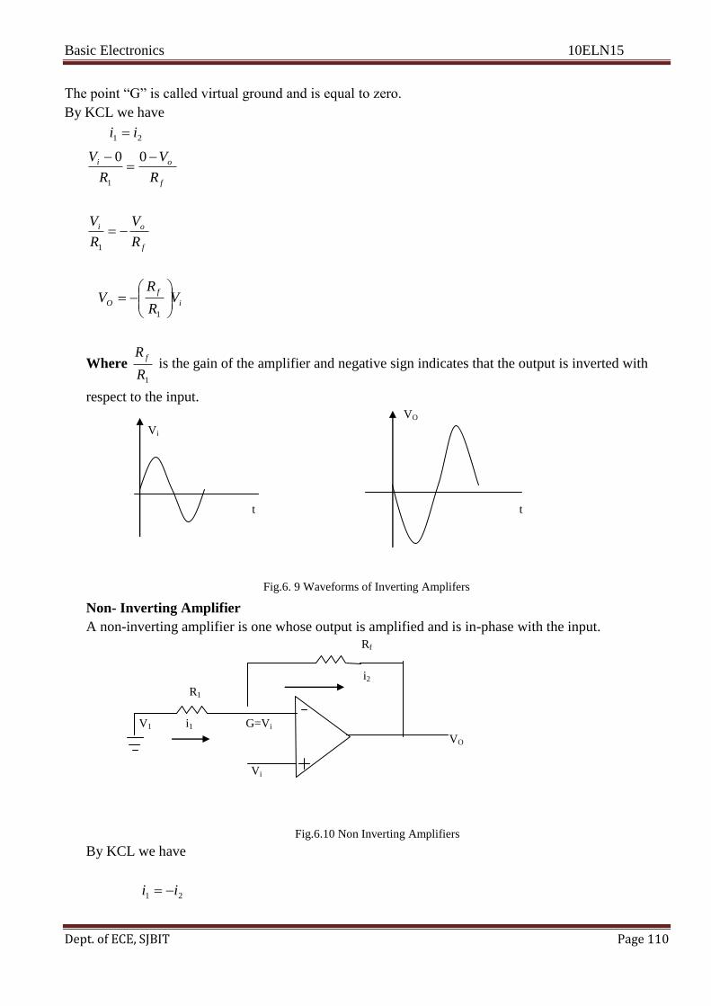
Basic Electronics 10ELN15
Dept. of ECE, SJBIT Page 110
The point ―G‖ is called virtual ground and is equal to zero.
By KCL we have
21 ii
f
oi
R
V
R
V
00
1
f
oi
R
V
R
V
1
i
f
O VR
RV
1
Where 1R
R f is the gain of the amplifier and negative sign indicates that the output is inverted with
respect to the input.
VO
Vi
t t
Fig.6. 9 Waveforms of Inverting Amplifers
Non- Inverting Amplifier
A non-inverting amplifier is one whose output is amplified and is in-phase with the input.
Rf
i2
R1
V1 i1 G=Vi
VO
Vi
Fig.6.10 Non Inverting Amplifiers
By KCL we have
21 ii

Basic Electronics 10ELN15
Dept. of ECE, SJBIT Page 111
f
Oii
R
VV
R
V
1
0
1
0
1
R
R
V
ViV
R
VV
R
V
f
i
f
iOi
1
1R
R
V
V f
i
O
i
f
i
O
R
R
V
V1
i
fV
R
RV
1
0 1
Where
1
1R
R fis the gain of the amplifier and + sign indicates that the output is in-phase
with the input.
Voltage follower
VO
Vi VO
Vi
t t
Fig. 6.11 Voltage follower
Voltage follower is one whose output is equal to the input.
The voltage follower configuration shown above is obtained by short circuiting ―Rf‖ and open circuiting
―R1‖ connected in the usual non-inverting amplifier.
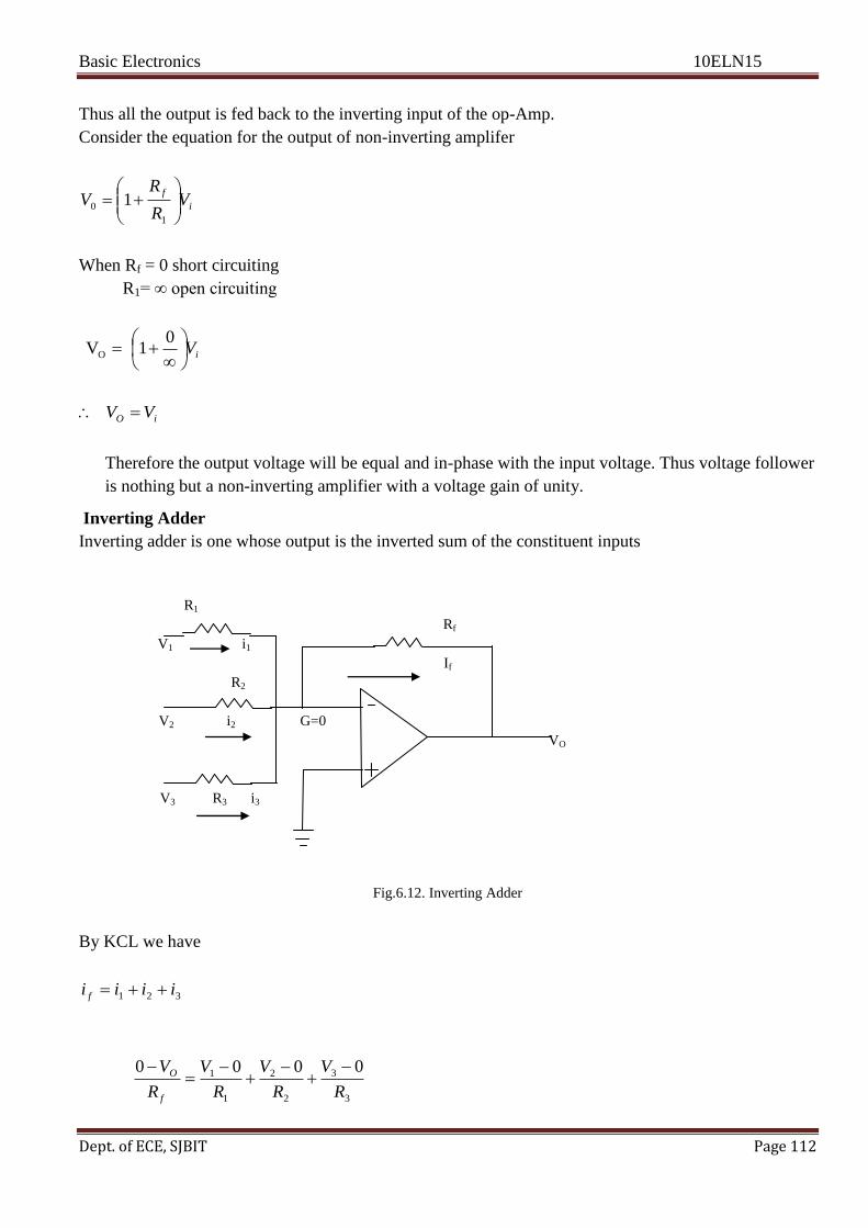
Basic Electronics 10ELN15
Dept. of ECE, SJBIT Page 112
Thus all the output is fed back to the inverting input of the op-Amp.
Consider the equation for the output of non-inverting amplifer
i
fV
R
RV
1
0 1
When Rf = 0 short circuiting
R1= ∞ open circuiting
iV
01V O
iO VV
Therefore the output voltage will be equal and in-phase with the input voltage. Thus voltage follower
is nothing but a non-inverting amplifier with a voltage gain of unity.
Inverting Adder
Inverting adder is one whose output is the inverted sum of the constituent inputs
R1
Rf
V1 i1
If
R2
V2 i2 G=0
VO
V3 R3 i3
Fig.6.12. Inverting Adder
By KCL we have
321 iiii f
3
3
2
2
1
1 0000
R
V
R
V
R
V
R
V
f
O

Basic Electronics 10ELN15
Dept. of ECE, SJBIT Page 113
3
3
2
2
1
1
R
V
R
V
R
V
R
V
f
O
3
3
2
2
1
1
R
V
R
V
R
VRV fO
If R1 = R2 = R3 =R then
321 VVVR
RV
f
O
If Rf = R then
VO = -[ V1 + V2 + V3 ]
Hence it can be observed that the output is equal to the inverted sum of the inputs.
Integrator
C
i2
R1
V1 i1 G=0
VO
Fig, 6.13 Integrator
An integrator is one whose output is the integration of the input.,
By KCL we have,
121 ii

Basic Electronics 10ELN15
Dept. of ECE, SJBIT Page 114
iO
Oi
O
O
O
O
ii
VRCdt
dV
dt
dVC
R
V
haveweinandgsubstituin
dt
dVCiei
iCdt
dV
dtiC
V
dtiC
V
havewesimilarlyand
R
V
R
Vi
havewefigureabovetheFrom
1
132
3..
1
1
10
20
2
2
2
2
1
dtVRC
V iO 1
Differentiator
A differentiator is one whose output is the differentiation of the input
R
i2
V1 i1 G=0
VO
By KCL we have

Basic Electronics 10ELN15
Dept. of ECE, SJBIT Page 115
R
V
dt
dVC
haveweinandngsubstituti
R
V
R
Vi
havewesimilarlyand
dt
dVCi
iCdt
dV
dtiC
V
havewefigureabovetheFrom
ii
Oi
OO
i
i
i
132
30
2.
1
1
1
2
1
1
1
21
dt
dVRCVO

Basic Electronics 10ELN15
Dept. of ECE, SJBIT Page 116
UNIT 7
COMMUNICATION SYSTEMS
Radio Broadcasting, Transmission and Reception
Radio communication means the radiation of radio waves by the transmitting station, the propagation of
these waves through space and their reception by the radio receiver.
Fig.7.1 below shows the general principle of radio broadcasting, transmission and reception. It
essentially consists of transmitter, transmission of radio waves and radio receiver.
Rxg antenna
Transmitting
Antenna
Fig7.1: Block diagram of Communication system
Transmitter-
It essentially consists of microphone, audio amplifiers, oscillator and modulator.
A microphone is a device which converts sound waves into electrical waves. The output of microphone
is fed to multistage audio amplifier for raising the strength of weak signal.The job of amplification is
performed by cascaded audio amplifiers. The amplified output from the last audio amplifier is fed to the
modulator for rendering the process of modulation.The function of the oscillation is to produce a high
frequency signal called a carrier wave. Usually crystal oscillator is used for the purpose.The amplified
audio signal and carrier waves are fed to the modulator. Here the audio signal is superimposed on the
carrier wave in suitable manner. The resultant waves are called modulated waves, and the process is
called modulation. The process of modulation permits the transmission of audio signal at the carrier
signal (frequency). As the carrier frequency is very high, therefore the audio signal can be transmitted to
large distances. The radio waves from the transmitter are fed to the transmitting antenna or aerial from
where these are radiated into space.
The transmitting antenna radiates the radio waves in space in all directions. These radio waves travel
with the velocity of light 3x10⁸m/sec. The radio waves are electromagnetic waves and possess the same
general properties.
Audio
Amplifiers
Oscillator Modulator
Radio
receiver

Basic Electronics 10ELN15
Dept. of ECE, SJBIT Page 117
Receiver-
On reaching the receiving antenna, the radio waves induce tiny emf in it. This small voltage is fed to the
radio receiver. Here the radio waves are first amplified and then signal is extracted from them by the
process of demodulation. The signal is amplified by audio amplifiers and then fed to the speaker for
reproduction into sound waves.
Need for modulation
The advantages of using modulation technique is given below :
Reduce the height of the antenna
Increase the range of communication
Avoids mixing of signals
Allows multiplexing of signals
Improves the signal to noise ratio.
Avoids interference of the bands by providing gaurd band
Improve quality of reception
Provide possibility for wireless transmission.
1. Practical Antenna length-theory shows that in order to transmit a wave effectively the length of the
transmitting antenna should be approximately equal to the wavelength of the wave.
metresHzfrequencyfrequency
Velocitywavelength
)(
103 8
As the audio frequencies range from 20 Hz to 20Khz, if they are transmitted directly into space, the
length of the transmitting antenna required would be extremely large. For example to radiate a frequency
of 20 KHz directly into space we would need an antenna length of 3x10⁸ /20x10
3 ≈ 15,000 meters. This
is too long to be constructed practically. But instead we operate at higher frequencies, say in MHz range,
the antenna dimension comes down.The operation at this frequencies is possible only with modulation
techniques.
2. Operating Range- The energy of a wave depends upon its frequency. The greater the frequency of
the wave, the greater the energy possessed by it. As the audio signal frequencies are small, therefore
these cannot be transmitted over large distances if radiated directly into space.
3. Avoids mixing of signals : The transmission band of 20Hz to 20KHz contains many signals
generated from different sources. These signals are translated to different portion of the
electromagnetic spectrum called channels, having different band widths, by providing different
carrier frequencies.These frequencies are separated at the receiver while receiving.
4. Allows multiplexing of signals; The modulation permits multiplexing of signals, meaning
simultaneous transmission of more signals on the same channel.Example MW and SW transmission
with frequencies allotted to different bands and transmitted on the same channel
5. Improves the signal to noise ratio.: The baes band signals which are in the audio frequency range
are susceptible to noise. The radio frequencies which are used for modulation are immune to noise.
Hence modulating the message signals with the carrier helps in improving the signal to noise ratio.

Basic Electronics 10ELN15
Dept. of ECE, SJBIT Page 118
6. Avoids interference of the bands by providing gaurd band : Special guard bandsare provided
between bands to guard the interference of adjacent band signals.This is usually around 25KHz.
7. Improve quality of reception : Different techniques of transmission like digital modulation
improves the quality of reception by reducing the noise in the system.
8. Wireless communication- Radio transmission should be carried out without wires.
Modulation- The process of changing some characteristics (example amplitude, frequency or phase) of
a carrier wave in accordance with the intensity of the signal is known as modulation.
Types of modulation-
1. Amplitude modulation
2. Frequency modulation
3. Phase modulation
1. Amplitude modulation
When the amplitude of high frequency carrier wave is changed in accordance with the intensity of the
signal, it is called amplitude modulation.
The following points are to be noted in amplitude modulation .
1. The amplitude of the carrier wave changes according to the intensity of the signal.
2. The amplitude variations of the carrier wave is at the signal frequency fS.
3. The frequency of the amplitude modulated wave remains the same ie.carrier frequency fC.
es
t
ec
t
e
t
Fig7.2: AM waveforms

Basic Electronics 10ELN15
Dept. of ECE, SJBIT Page 119
Modulation factor
The ratio of change of amplitude of carrier wave to the amplitude of normal carrier wave is called
modulation factor.
m=(amplitude change of carrier wave) / normal carrier wave(unchanged)
A + No Signal =
carrier m=0/A = 0%
2A
+ =
carrier signal
m=(2A-A)/A =1
Modulation factor is very important since it determines the strength and quality of the transmitted signal.
The greater the degree of modulation, the stronger and clearer will be the audio signal. It should be noted
that if the carrier is overmodulated (ie m>1) distortion will occur at reception.
Analysis of amplitude modulated wave
signal
mEc
EC Ec
Carrier
AM Wave
A carrier wave is represented by ec = Eccoswct-------------------(1)

Basic Electronics 10ELN15
Dept. of ECE, SJBIT Page 120
Where ec ------instantaneous voltage of carrier.
Ec -----amplitude of carrier.
In amplitude modulation, the amplitude EC of the carrier wave is varied in accordance with
intensity of the signal as shown in figure.
Suppose m=modulation index, then change in carrier amplitude =mEc.
Amplitude or Emax of the signal = mEc.
es =mEccoswst---------------------------------(2)
where mEc is the amplitude of the signal.
es ---------instantaneous voltage of the signal.
The amplitude of the carrier varies at signal frequency fs. Therefore the amplitude of AM wave is given
by,
Ec +mEccoswst = Ec(1+mcoswst)
The instantaneous voltage of AM wave is,
e = Amplitude x coswct
)3()cos(2
)cos(2
cos
])cos()[cos(2
cos
]coscos2[2
cos
coscoscos
cos)cos1(
twwmE
twwmE
twEe
twwtwwmE
twE
twtwmE
twE
twtwmEtwE
twtwmEe
scc
scc
cC
scscc
cC
csC
cC
csCcC
csC
The AM wave is equivalent ot thesummatoin of theree sinusoidal waves: aone having amplitude
EC and frequency fc, the second having amplitde mEc/2 and frequency (fc + fs) and the third
having amplitude mEc/2 and frequency fc – fs..
The AM wave consists three frequencies viz, fc, fc+fs . The first frequency is the carrier frequency.
Thus the process of modulation doesnot change the original carrier frequency but produces two
new frequencies fc+fs and fc – fs. which are called sideband frequencies.
In amplitude modulation the bandwidth is from fc – fs. to fc+fs ie 2fs ie twice the signal frequency.
Frequency spectrum of an amplitude modulated wave is shown in figure below
EC
mEC/2
fC-fS fC fC+fS frequency
Fig7.3: Frequency Spectrum of AM wave

Basic Electronics 10ELN15
Dept. of ECE, SJBIT Page 121
)7(2)6(
)5(
,
)6(2
2
2
21
242
)5(4
2222
)4(2
2
),3(
2
2
22
22222
22
22
2
2
m
m
equn
equn
P
P
sidebandsbycarriedpowertotaloffractionAlso
m
R
E
m
R
E
R
Em
R
E
PPPwaveAMofpowerTotal
R
Em
R
mE
R
mE
PsidebandsofpowerTotal
R
E
R
E
Ppowercarrier
equationfrom
T
S
C
CCC
SCT
C
CC
S
C
c
C
Limitations of Amplitude Modulation
1. Noisy Reception- In an AM wave, the signal is in the amplitude variations of the carrier.
Practically all the natural and man made noises consist of electrical amplitude disturbances. As a
radio receiver cannot distinguish between amplitude variations that represent noise and those that
contain the desired signal. Therefore reception is very noisy.
2. Low efficiency- In AM useful power is in the sidebands as they contain the signal. An AM wave
has low sideband power.
For example even if modulation is 100 % ie m=1.
33.012
1
2 2
2
m
m
p
P
T
S
PS=33% of PT
Sideband power is only one-third of the total power of AM wave. Hence efficiency of this type of
modulation is low.
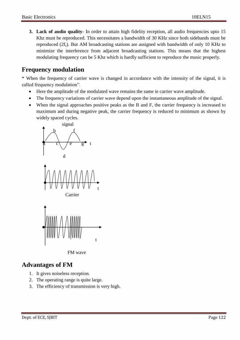
Basic Electronics 10ELN15
Dept. of ECE, SJBIT Page 122
3. Lack of audio quality- In order to attain high fidelity reception, all audio frequencies upto 15
Khz must be reproduced. This necessitates a bandwidth of 30 KHz since both sidebands must be
reproduced (2fs). But AM broadcasting stations are assigned with bandwidth of only 10 KHz to
minimize the interference from adjacent broadcasting stations. This means that the highest
modulating frequency can be 5 Khz which is hardly sufficient to reproduce the music properly.
Frequency modulation
“ When the frequency of carrier wave is changed in accordance with the intensity of the signal, it is
called frequency modulation‖.
Here the amplitude of the modulated wave remains the same ie carrier wave amplitude.
The frequency variations of carrier wave depend upon the instantaneous amplitude of the signal.
When the signal approaches positive peaks as the B and F, the carrier frequency is increased to
maximum and during negative peak, the carrier frequency is reduced to minimum as shown by
widely spaced cycles.
signal
b f
a c e g t
d
t
Carrier
t
FM wave
Advantages of FM
1. It gives noiseless reception.
2. The operating range is quite large.
3. The efficiency of transmission is very high.

Basic Electronics 10ELN15
Dept. of ECE, SJBIT Page 123
Comparision of AM and FM.
Amplitude Modulation Frequency Modulation
1) The amplitude of the carrier is varied The frequency of the carrier is varied
In accordance with the signal in accordance with the signal
2) The modulation index ‗m‘ is <1 The modulation index ‗β‘ is >1
3) Transmitted power is dependent Transmitted power is independent
on modulation index ‗m‘ on modulation index ‗β‘
4) The amplitude of the side bands are The amplitude of the side bands are
dependent on the modulation index‘m‘ vary with the modulating index and
and are always less than the carrier can be calculated using Bessel functions
5) Contains only two side bands Contains multiple side bands
6) Susceptible to noise due to Immune to noise as amplitudes are
The method of modulation used. Clipped
7) Less efficient as carrier contains More efficient as it contains more side
more power than side bands bands and hence more signal power.
8) De-modulation is simple De-modulation is more complex.
Demodulation
The process of recovering the audio signal from the modulated wave is known as demodulation or
detection.
At the broadcasting station, modulation is done to transmit the audio signal over larger distances.
When the modulated wave is picked up the receiver, it is necessary to recover the audio signal from
it. This process is accomplished in the radio receiver and is called demodulation.
AM diode detector
Fig. below shows a simple diode detector employing a diode and a filter circuit. A detector circuit
performs the following two functions.
1. It rectifies the modulated wave.
2. It separates the audio signal from the carrier.

Basic Electronics 10ELN15
Dept. of ECE, SJBIT Page 124
Speaker
Audio output
Rectified
Wave
AM Wave
Fig7.4: AM Diode detector
The modulated wave of desired frequency is selected by the parallel tuned circuit L1C1 and is
applied to the diode. During positive half cycles of the modulated wave the diode conducts, while
during negative half cycles it doesnot. The result is the output of diode consists of positive half
cycle of modulated wave as shown in figure.
The rectified output consists of r.f. component and the audio signal which cannot be fed to the
speaker for sound reproduction. The r.f. component is filtered by the capacitor ‗C‘ shunted
across the speaker. The value of ‗C‘ is large enough to present low reactance to the r.f.
component . fc+fs Therefore signal is passed to the speaker.
AM Radio Receiver
In order to reproduce the AM wave into sound waves, every radio receiver must perform the following
functions.
1. The receiving aerial must intercept a portion of the passing radio waves.
2. The radio receiver must select the desired radio from a number of radio waves intercepted
by the receiving aerial. For this purpose tuned parallel LC circuits must be used. These
circuits will select only that radio frequency which is resonant with them.
3. The selected radio wave must be amplified by the tuned frequency amplifiers.
4. The audio signal must be recovered from the amplified radio wave.
5. The audio signal must be amplified by suitable number of audio-amplifiers.
Types of AM radio receivers
1. Straight Radio receiver
2. Superhetrodyne radio receiver

Basic Electronics 10ELN15
Dept. of ECE, SJBIT Page 125
1. Straight Radio Receiver
Receiving antenna
RF amplifier
Fig7.5: Straight Radio Receiver
The Receiving antenna is receiving radio waves from different broadcasting stations. The desired
radio wave is selected by the tuned RF amplifer which employs tuned parallel circuit. The
selected radio wave is amplified by the rf amplifier.
The amplified radio wave is fed to the detector circuit. This circuit extracts the audio signal from
the radio wave. The output of the detector is the audio signal which is amplified by one or more
stages of audio-amplifications. The amplified audio signal is fed the speaker for sound
reproduction.
Limitations-
1. In straight radio receivers, tuned circuits are used. As it is necessary to change the value of a
variable capacitors (gang capacitors) for tuning to the desired station, there is a considerable
variation of Q between the closed and open positions of the variable capacitors. This changes the
sensitivity and selectivity of the radio receivers.
2. There is too much interference of adjacent stations.
Superhetrodyne Receiver
Here the selected radio frequency is converted to a fixed lower value called intermediate frequency (IF).
This is achieved by special electronic circuit called mixer circuit. The production of fixed intermediate
frequency (455 KHz) is an important feature of superhetrodyne circuit. At this fixed intermediate
frequency, the amplifier circuit operates with maximum stability, selectivity and sensitivity.
The block diagram of superhetrodyne receiver is a shown in fig7.6 below.
Receiving antenna
Detector
AF
amplifier

Basic Electronics 10ELN15
Dept. of ECE, SJBIT Page 126
C3 L3
c2
RF amplifier Mixer 455KHz
L2
Speaker
Local oscillator
Fig7.6: Superhetrodyne Receiver
1. RF amplifier stage- The RF amplifier stage uses a tuned parallel circuit L1C1 with a variable
capacitor C1. The radio waves from various broadcasting stations are intercepted by the receiving
aerial and are coupled to this stage. This stage selects the desired radio wave and raises the
strength of the wave to the desired level.
2. Mixer stage- The amplified output of RF amplifier is fed to the mixer stage where it is combined
with the output of a local oscillator. The two frequencies beat together and produce an
intermediate frequency (IF).
IF= Oscillator frequency –radio frequency
The IF is always 455 KHz regardless of the frequency to which the receiver is tuned. The reason why
the mixer will always produce 455KHz frequency above the radio frequency is that oscillator always
produces a frequency 455KHz above the selected frequency. In practice, capacitance of C3 is
designed to tune the oscillator to a frequency higher than radio frequency by 455KHz.
3. IF amplifier stage- The output of mixer is always 455KHz and is fed to fixed tuned IF
amplifiers. These amplifiers are tuned to one frequency (ie 455KHz).
4. Detector stage- The output from the last IF amplifier stage is coupled to the input of the detector
stage. Here the audio signal is extracted from the IF output. Usually diode detector circuit is used
because of its low distortion and excellent audio fidelity.
5. AF amplifier stage- The audio signal output of detector stage is fed to a multistage audio
amplifier. Here the signal is amplified until it is sufficiently strong to drive the speaker. The
speaker converts the audio signal into sound waves corresponding to the original sound at the
broadcasting station.
Detector
AF
amplifier
IF
Amplifier

Basic Electronics 10ELN15
Dept. of ECE, SJBIT Page 127
Advantages of Superhetrodyne Circuit –
1. High RF amplification
2. Improved selectivity-losses in the tuned circuits are lower at intermediate frequency. Therefore
the quality factor Q of the tuned circuits is increased. This makes amplifier circuits to operate
with maximum selectivity.
3. Lower cost.
CATHODE RAY OSCILLOSCOPE
The cathode ray oscilloscope [CRO] is an electronic device, which is capable of giving a visual
indication of a signal waveform. It is widely used for trouble shooting radio and television receivers as
well as laboratory work involving research and design. In addition the oscilloscope can also be used for
measuring voltage, frequency and phase shift.
Cathode Ray Tube
A cathode ray tube is the heart of the oscilloscope. It is a vacuum tube of special geometrical shape and
converts an electrical signal into visual one. A cathode ray tube makes available plenty of electrons.
These electrons are accelerated to high velocity and are brought to focus on a fluorescent screen. The
electron beam produces a spot of light wherever it strikes. The electron beam is deflected on its journey
in response to the electrical signal under study. The result is that electrical signal waveform is displayed
visually.
Fig7.7: Cathode Ray Tube
Electron Gun Assembly- The arrangement of electrodes which produce a focused beam of electrons
is called the electron gun. It essentially consists of an indirectly heated cathode, control grid, a
focusing anode, and an accelerating anode. The control grid is held at negative potential with respect
to cathode whereas the two anodes are maintained at high potential with respect to cathode.

Basic Electronics 10ELN15
Dept. of ECE, SJBIT Page 128
The cathode consists of a nickel cylinder coated with oxide coating and provides plenty of electrons.
The focusing anode focuses the electron beam into a sharp pin –point by controlling the positive
potential on it. The positive potential ( about 10,000 V) on the accelerating anode is much higher
than on the focusing anode. Therefore this anode accelerates the narrow beam to a high velocity.
Deflection plate assembly-
1. Vertical deflection plates
2. Horizontal deflection plates
The vertical deflection plates are mounted horizontally in the tube. By applying proper potential to these
plates, the electron beam can be made to move up and down vertically on the fluorescent screen. An
appropriate potential on horizontal plates can cause the electron beam to move right and left horizontally
on the screen.
Screen-The screen is the inside face of the tube and is coated with some fluorescent material such
as Zinc Orthosilicate, Zinc oxide etc. When high velocity electron beam strikes the screen, a spot of
light is produced at the point of impact.
Action of CRT
O1
+ + + + + +
_ _ _ _ _ _ O
O2
When the cathode is heated, it emits plenty of electrons. The control grid influences the amount
of current flow. As the electron beam leaves the control grid, it comes under the influence of
focusing and accelerating anode. As the two anodes are maintained at high potential, therefore
they produce a field which acts as an electrostatic lens to converge the electron beam at a point
on the screen.
As the electron beam leaves the accelerating anode, it comes under the influence of vertical and
horizontal deflection plates. If no voltage is applied to the deflection plates, the electron will
produce spot of light at the center (point O ) of the screen. If the voltage is applied to vertical
plates only, the electron beam and hence the spot of light will be deflected upwards (point O1 ).
The spot of light will be deflected downwards (O2) of the portential on the plate is reversed.
Similarly the spot of light can be moved horizontally by applying voltage across the horizontal
plates.

Basic Electronics 10ELN15
Dept. of ECE, SJBIT Page 129
Signal Pattern on Screen
CRO Screen
2
1 3 5
t
4
_ +
Sawtooth wave applied across horizontal plate
If the signal voltage is applied to the vertical plates and saw tooth wave to the horizontal plates,
we get the exact pattern of the signal as shown in figure.
When the signal is at instant 1, its amplitude is zero. But at this instant, maximum voltage is
applied to the horizontal plates. The result is that the beam is at the extreme left on the screen as
shown. When the signal is at instant 2, its amplitude is maximum. However the –ve voltage on he
horizontal plate is decreased. Therefore the beam is deflected upwards by the signal and towards
the right by the saw tooth wave. The result is that the beam now strikes the screen at point 2. On
similar reasoning, the beam strikes the screen at points 3,4 and 5. Therefore exact signal pattern
appears on the screen.
Various controls on CRO
In order to facilitate the proper functioning of CRO, various controls are provided on the front panel of
the CRO.
1. Intensity Control-The knob of intensity control regulates the bias on the control grid and affects
the electron beam intensity.If the negative bias on the grid is increased, the intensity of electron
beam is decreased, thus reducing the brightness of the spot.
2. Focus Contrl- It regulates the positive potential on the focusing anode. If the positive potential
on this anode is increased, the electron beam becomes quite narrow and the spot on the screen is
a pin-point.
2
1 3 5
4

Basic Electronics 10ELN15
Dept. of ECE, SJBIT Page 130
3. Vertical position control- The knob of vertical position control regulates the amplitude of d.c.
potential which is applied to the vertical deflection plates in addition to the signal. By adjusting
this control, the image can be moved up or down as required.
Measurement using CRO
The various characteristics of an input signal and the property of the signal such as voltage, current,
frequency, period, phase, amplitude,peak to peak values, duty cycle etc.can be measured using CRO.
Voltage Measurement
The CROM includes the amplitude measurement facilities such as constant gain amplifiers and the
calibrated shift controls.The waveform can be adjusted on the screen using shift controls so that the
measurement of divisions corresponding to the amplitude become easy.
The follwing steps are used for measurement of amplitude :
1) Apply the wave form to one of the inputs and adjust the controls on the oscilloscope until a still
waveform is obtained on the screen
2) Note down the Volts/Division readings from the front panel.
3) Note down the peak to peak divisions.
4) Use the following relation to obtain the peak to peak value.
Vpp= Number of divisions * (Volts/Division)
Now Vpeak=Vpp/2
And Vrms =Vpeak/1.414
Period and frequency measurement
Display the waveform on the screen such that one complete cycle is visible on the screen. Note the
time/division selected on the front panel.
Now, time period T =(no. of divisions o0n time base)*time/division
Frequency measurement
From the time period T , the frequency can be obtained as :
Frequency f = 1/T.
Phase measurement
The phase measurement is possible by time measurement by actually measuring the phaseshift
between the two signals
The steps followed are :
1) Display the two signals using dual channels of the oscilloscope
2) Using the ground position of the control switch AC GND DC align the time bases of both the
channels with the horizontal lines
3) Using AC position of the switches display both the signals
4) Now measure the phase difference between the signals interms of no. of divisions say ΘT
5) Measure the time period T of both the signals .
6) Now calculate ΘT as
ΘT =Θ *360/T
=
Applications of CRO
1. Examination of waveforms
2. Voltage measurements
3. Frequency measurementseries
Basic Electronics 10ELN15
Dept. of ECE, SJBIT Page 131
NUMBER SYSTEM
The human need to count things goes back to the dawn of civilization. To answer the questions like
―how much‖, or ―how many‖, people invented number system. A number system is any scheme used to
count things. The decimal number system succeeded because very large numbers can be expressed using
relatively short series of easily memorized numerals. Decimal or base 10 number system‘s origin: can be
traced to, counting on the fingers with digits. ―Digit‖ taken from the Latin word digitus meaning ―finger‖
In any number system, the important terms to be known are :
Base or radix, numerals, positional value, absolute value, radix point and the prevalent number systems
of interest for study.
Base: Base is the number of different digits or symbols or numerals used to represent the number system
including zero in the number system. It is also called the radix of the number system.
Numeral : Numeral is the symbols used to represent the number system
Each digit in the number system has two values:
a) Absolute value
b) Positional value
The absolute value is the value of the digit itself, representing the no. system. The positional value is
the value it possesses by virtue of its position in the no. system
The different number systems of interest for study, from the point of view of application to computers
are:
Examples of commonly used number systems :
decimal
binary
octal
hexadecimal.
Important properties of these systems need to be studied.
Polynomial Notation (Series Representation) :Any number system can be represented by the following
polynomial.
N = an-1 x rn-1 + an-2 x rn-2 + .. + a0 x r0 + a-1 x r-1 ... + a-m x r–m Where
r = radix or base
n = number of integer digits to the left of the radix point
m = number of fractional digits to the right of the radix point
an-1 = most significant digit (MSD)
a-m = least significant digit (LSD)
Example:
N = (251.41)10 = 2 x 10² + 5 x 101 + 1 x 100 + 4 x 10⁻¹ + 1 x 10⁻²
Decimal number system :
The decimal system is composed of 10 numerals or symbols. These 10 symbols are 0, 1, 2, 3, 4, 5, 6, 7, 8,
9. Using these symbols as digits of a number, we can express any quantity. The decimal system is also
called the base-10 system because it has 10 digits.

Basic Electronics 10ELN15
Dept. of ECE, SJBIT Page 132
In decimal system, the no. 1000.111 is represented as:
Integer part Fractional part
103 10
2 10
1 10
0 10
-1 10
-2 10
-3
=1000 =100 =10 =1 . =0.1 =0.01 =0.001
Most Significant Digit Decimal point
Least
Significant
Digit
Example : Multiply the value of the symbol by the value of the position, then add
In decimal, 1954.89means
1 times 1,000
plus 9 times 100
plus 5 times 10
plus 4 times 1
plus 8 times 1/10
plus 9 times 1/100 = The number is 1954.89 in decimal. and is represented by (1954.89)10. The digits
are separated by a point “.” called the radix point. In decimal system it is called ―decimal point‖.
Decimal Examples of decimal numbers
1410
5210
102410
6400010
Binary number system :
In the binary system, there are only two symbols or possible digit values, 0 and 1. This base-2 system
can be used to represent any quantity that can be represented in decimal or other base system.
Integer part Fractional part
23 2
2 2
1 2
0 2
-1 2
-2 2
-3
=8 =4 =2 =1 . =0.5 =0.25 =0.125
Most Significant Digit Binary point
Least
Significant
Digit
Binary Counting
The Binary counting sequence to represent decimal numbers is shown in the table below :
23 2
2 2
1 2
0 Decimal
0 0 0 0 0
0 0 0 1 1
0 0 1 0 2
0 0 1 1 3

Basic Electronics 10ELN15
Dept. of ECE, SJBIT Page 133
0 1 0 0 4
0 1 0 1 5
0 1 1 0 6
0 1 1 1 7
1 0 0 0 8
1 0 0 1 9
1 0 1 0 10
1 0 1 1 11
1 1 0 0 12
1 1 0 1 13
1 1 1 0 14
1 1 1 1 15
Representing Binary Quantities
In digital systems the information that is being processed is usually presented in binary form. Any device
that has only two operating states or possible conditions can represent binary quantities. E.g.. a switch
which can be either be only open or closed. We arbitrarily (as we define them) let an open switch
represent binary 1 and a closed switch represent binary 0. Thus we can represent any binary number by
using series of switches.
Typical Voltage Assignment
Binary 1: Any voltage between 2V to 5V
Binary 0: Any voltage between 0V to 0.8V
Not used: Voltage between 0.8V to 2V in 5 Volt CMOS and TTL Logic is not used as it may cause error
in a digital circuit.
We can see another significant difference between digital and analog systems. In digital systems, the
exact voltage value is not important; eg, a voltage of 3.6V means the same as a voltage of 4.3V. In
analog systems, the exact voltage value is important
Binary addition and subtraction: Examples of addition and subtraction in this number system is shown
below:
The addition of binary numbers is done as follows:
a) 1 + 1 = 0 with a carry of 1, and can be represented as (10)2 , with 0 taking LSD position and 1
taking MSD.
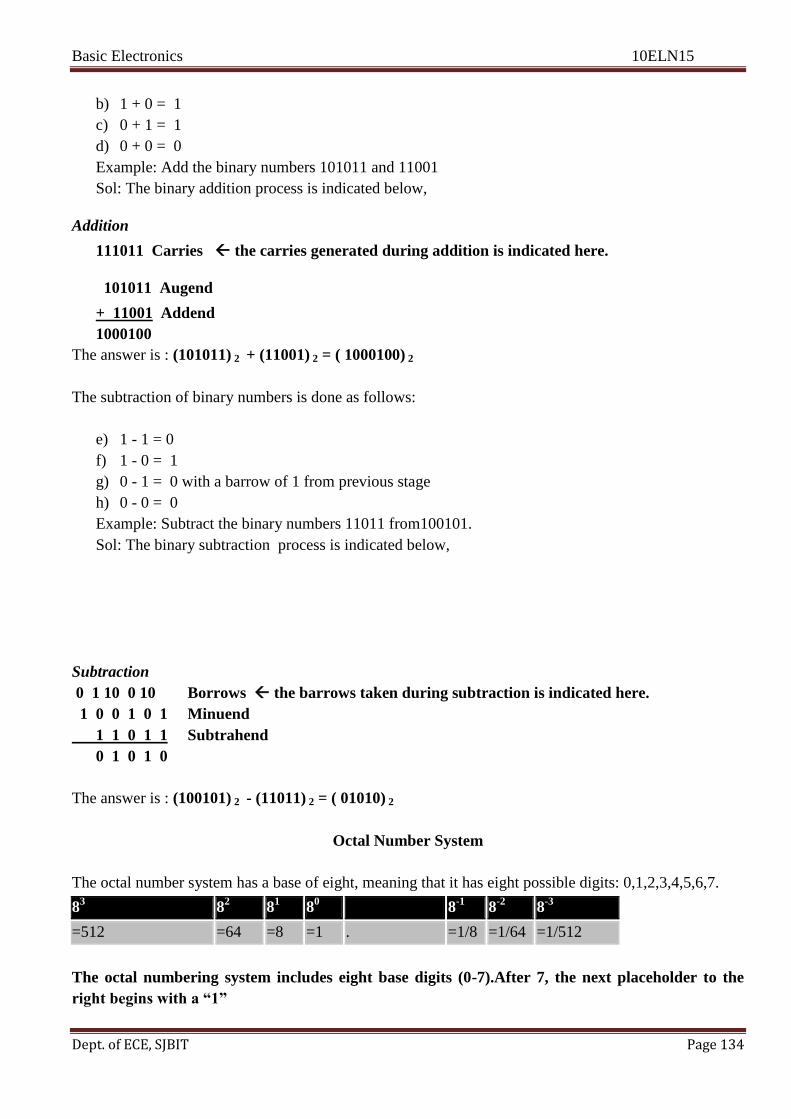
Basic Electronics 10ELN15
Dept. of ECE, SJBIT Page 134
b) 1 + 0 = 1
c) 0 + 1 = 1
d) 0 + 0 = 0
Example: Add the binary numbers 101011 and 11001
Sol: The binary addition process is indicated below,
Addition
111011 Carries the carries generated during addition is indicated here.
101011 Augend
+ 11001 Addend
1000100
The answer is : (101011) 2 + (11001) 2 = ( 1000100) 2
The subtraction of binary numbers is done as follows:
e) 1 - 1 = 0
f) 1 - 0 = 1
g) 0 - 1 = 0 with a barrow of 1 from previous stage
h) 0 - 0 = 0
Example: Subtract the binary numbers 11011 from100101.
Sol: The binary subtraction process is indicated below,
Subtraction
0 1 10 0 10 Borrows the barrows taken during subtraction is indicated here.
1 0 0 1 0 1 Minuend
1 1 0 1 1 Subtrahend
0 1 0 1 0
The answer is : (100101) 2 - (11011) 2 = ( 01010) 2
Octal Number System
The octal number system has a base of eight, meaning that it has eight possible digits: 0,1,2,3,4,5,6,7.
83 8
2 8
1 8
0 8
-1 8
-2 8
-3
=512 =64 =8 =1 . =1/8 =1/64 =1/512
The octal numbering system includes eight base digits (0-7).After 7, the next placeholder to the
right begins with a “1”

Basic Electronics 10ELN15
Dept. of ECE, SJBIT Page 135
0, 1, 2, 3, 4, 5, 6, 7, 10, 11, 12, 13 ...
Octal to Decimal Conversion
2378 = 2 x (82) + 3 x (8
1) + 7 x (8
0) = 15910
24.68 = 2 x (81) + 4 x (8
0) + 6 x (8
-1) = 20.7510
11.18 = 1 x (81) + 1 x (8
0) + 1 x (8
-1) = 9.12510
12.38 = 1 x (81) + 2 x (8
0) + 3 x (8
-1) = 10.37510
Octal addition and subtraction:
Examples of addition and subtraction in this number system is shown below:
Example: Add the octal numbers 5471 and 3754
Sol : The addition process with procedure is shown below :
Addition
1 1 1 Carries the carries generated during addition is indicated here.
5 4 7 1 Augend
+ 3 7 5 4 Addend
1 1 4 4 5 Sum
Procedure :
Addition of first column 1+4= 5
Addition of second column 7+5= 12 and 12-8 = 4, with a carry of 1 to left
Addition of third column 1+4+7= 12 and 12-8 = 4, with a carry of 1 to left
Addition of fourth column 1+5+3= 9 and 9-8 = 1, with a carry of 1 to left
The final carry forms the MSD.
The answer is : (5471) 8 + (3754) 8 = ( 11445) 8
Subtraction
Example: Subtract the octal numbers 7451 and 5643
Sol : The subtraction process with procedure is shown below :
6 10 4 10 Borrows the barrows taken during subtraction is indicated here.
7 4 5 1 Minuend
- 5 6 4 3 Subtrahend
1 6 0 6 Difference
Procedure :
Subtraction of first column 1-3= 6,by borrowing carry from previous stage
1+8= 9, hence 9-3=6
Subtraction of second column 4-4= 0,now after the barrow 5 becomes 4 in II column.
Subtraction of third column 4-6= 6, by borrowing from previous stage, 8+4=12,
Hence 12-6 = 6
Subtraction of fourth column 6-5= 1, 7 will become 6 after a barrow to the right.

Basic Electronics 10ELN15
Dept. of ECE, SJBIT Page 136
The answer is : (7451) 8 - (5643) 8 = ( 1606) 8
Hexadecimal number system
The hexadecimal system uses base 16. Thus, it has 16 possible digit symbols. It uses the digits 0 through
9 plus the letters A, B, C, D, E, and F ,to represent 10 through 16, as the 16 digit symbols
Digits = 0, 1, 2, 3, 4, 5, 6, 7, 8, 9, A, B, C, D, E, F
(B65F)16 = 11 x 163 + 6 x 162 + 5 x 161 + 15 x 160 = (46,687)10
Sometimes, it is necessary to use a numbering system that has more than ten base digits
One such numbering system is hexadecimal number system, useful in computer application.
Hexadecimal number, is widely used in micro processors and micro controllers
in assembly programming, and in embedded system development.
Hexadecimal addition and subtraction: Examples of addition and subtraction in this number system is
shown below:
Addition
1 0 1 1 Carries
5 B A 9 Augend
+ D 0 5 8 Addend
1 2 C 0 1 Sum
Subtraction
9 10 A 10 Borrows
A 5 B 9 Minuend
+ 5 8 0 D Subtrahend
1 D A C Difference

Basic Electronics 10ELN15
Dept. of ECE, SJBIT Page 137
Conversion of number systems.
Converting from one no. system to another is called conversion of no. system or code conversion, like
converting from binary to decimal or converting from hexadecimal to decimal etc.The possibilities of
conversions of above number system is shown below.
Conversion Among Bases
The possibilities:
The binary number system is the most important one in digital systems, but several others are also
important. The decimal system is important because it is universally used to represent quantities outside
a digital system. This means that there will be situations where decimal values have to be converted to
binary values before they are entered into the digital system.
The above diagram shows all the possibilities of conversions discussed below. However the possibilities
of conversions can be summarized in to the following three categories :
Case 1: Conversion from decimal to other number system.
Case 2: Conversion from other number system to decimal number system.
Case 3: Conversion from among number systems other than decimal number system.
Hexadec
imal
Decimal Octal
Binary

Basic Electronics 10ELN15
Dept. of ECE, SJBIT Page 138
Binary-To-Decimal Conversion
The binary number system is the most important one in digital systems, but several others are also
important. The decimal system is important because it is universally used to represent quantities outside
a digital system. This means that there will be situations where decimal values have to be converted to
binary values before they are entered into the digital system.
Any binary number can be converted to its decimal equivalent simply by summing together the weights
of the various positions in the binary number which contain a
together the weights of the various positions in the binary number which contain a 1.
Technique
Multiply each bit by 2n, where n is the “weight” of the bit
The weight is the position of the bit, starting from 0 on the right
Add the results
Example:
Binary Decimal
101101012
27+0
6+2
5+2
4+0
3+2
2+0
1+2
0 =128+0+32+16+0+4+0+1
Result 18110
You should have noticed that the method is to find the weights (i.e., powers of 2) for each bit position
that contains a 1, and then to add them up.
Binary to decimal Fractions:
Example :
10.1011 => 1 x 2-4 = 0.0625
1 x 2-3 = 0.125
0 x 2-2 = 0.0
1 x 2-1 = 0.5
0 x 20 = 0.0
1 x 21 = 2.0
=2.6875
Procedure: Same principles with following exception ;.
Use negative powers of the base to the right of the radix point. (Only call it a decimal point in the
decimal number system.)
Decimal-To-Binary Conversion
There are 2 methods:
Reverse of Binary-To-Decimal Method
Repeat Division
Reverse of Binary-To-Decimal Method

Basic Electronics 10ELN15
Dept. of ECE, SJBIT Page 139
Example :
Decimal Binary
4510 =32 + 0 + 8 + 4 +0 + 1
=25+0+2
3+2
2+0+2
0
Result =1011012
Repeat Division-Convert decimal to binary
This method uses repeated division by 2.
Example :
Conversion of 2710 to binary
Division Remainder Binary
25/2 = 12+ remainder of 1 1 (Least Significant Bit)
12/2 = 6 + remainder of 0 0
6/2 = 3 + remainder of 0 0
3/2 = 1 + remainder of 1 1
1/2 = 0 + remainder of 1 1 (Most Significant Bit)
Result 2510 = 110012
Procedure :
Divide by two, keep track of the remainder
Group the remainders in the following order
First remainder is bit LSB (least-significant bit)
Last remainder is bit MSB (Most-significant bit)
Binary-To-Octal / Octal-To-Binary Conversion
Octal Digit 0 1 2 3 4 5 6 7
Binary
Equivalent 000 001 010 011 100 101 110 111
Each Octal digit is represented by three binary digits.
Example: 100 111 0102 = (100) (111) (010)2 = 4 7 28
Octal to decimal
Procedure
Multiply each bit by 8n, where n is the “weight” of the bit

Basic Electronics 10ELN15
Dept. of ECE, SJBIT Page 140
The weight is the position of the bit, starting from 0 on the right
Add the results.
Example:
724.258 => 4 x 80 = 4
2 x 81 = 16
7 x 82 = 448
2 x 1/8 = 0.25
5 x 1/82 = 0.015625
Ans: 7248 =468.26562510
Decimal to octal
Repeat Division-Convert decimal to octal : This method uses repeated division by 8.
Example: Convert 17710 to octal and binary
Division Result Binary
177/8 = 22+ remainder of 1 1 (Least Significant Bit)
22/ 8 = 2 + remainder of 6 6
2 / 8 = 0 + remainder of 2 2 (Most Significant Bit)
Result 17710 = 2618
Binary = 0101100012
Hexadecimal to Decimal/Decimal to Hexadecimal Conversion
Example: 2AF16 = 2 x (162) + 10 x (16
1) + 15 x (16
0) = 68710
Hexadecimal to Decimal Conversion
Technique
Multiply each bit by 16n, where n is the “weight” of the bit
The weight is the position of the bit, starting from 0 on the right
Add the results
Example:
ABC.6D16 => C x 160 = 12 x 1 = 12
B x 161 = 11 x 16 = 176
A x 162 = 10 x 256 = 2560
6 x 1/16 = 6 x .0625
D x 1/162 = 13 x .0039

Basic Electronics 10ELN15
Dept. of ECE, SJBIT Page 141
= 2748.066410
Ans: ABC16 = 2748.066410
24.616 = 2 x (161) + 4 x (16
0) + 6 x (16
-1) = 36.37510
11.116 = 1 x (161) + 1 x (16
0) + 1 x (16
-1) = 17.062510
12.316 = 1 x (161) + 2 x (16
0) + 3 x (16
-1) = 18.187510
Decimal To Hexadecimal
Repeat Division- Convert decimal to hexadecimal - This method uses repeated division by 16.
Example: convert 37810 to hexadecimal and binary:
Division Result Hexadecimal
378/16 = 23+ remainder of 10 A (Least Significant Bit)23
23/16 = 1 + remainder of 7 7
1/16 = 0 + remainder of 1 1 (Most Significant Bit)
Result 37810 = 17A16
Binary = 0001 0111 10102
Binary-To-Hexadecimal /Hexadecimal-To-Binary Conversion
Hexadecimal Digit 0 1 2 3 4 5 6 7
Binary Equivalent 0000 0001 0010 0011 0100 0101 0110 0111
Hexadecimal Digit 8 9 A B C D E F
Binary Equivalent 1000 1001 1010 1011 1100 1101 1110 1111
Each Hexadecimal digit is represented by four bits of binary digit
Example: 1011 0010 11112 = (1011) (0010) (1111)2 = B 2 F16
Octal-To-Hexadecimal, Hexadecimal-To-Octal Conversion
Convert Octal (Hexadecimal) to Binary first.
Regroup the binary number by three bits per group starting from LSB if Octal is required.
Regroup the binary number by four bits per group starting from LSB if Hexadecimal is required
Example:
Convert 5A816 to Octal.
Hexadecimal Binary/Octal
5A816 = 0101 1010 1000 (Binary)
= 010 110 101 000 (Binary)

Basic Electronics 10ELN15
Dept. of ECE, SJBIT Page 142
Result = 2 6 5 0 (Octal)
Complement method of subtraction
The complement method of subtraction is the method used for subtraction of numbers in different
number systems. This method is useful as it can easily implemented in arithmetic logic circuits and
inverting circuits in computers.
The complement method used in various no. systems discussed above is indicated below:
For decimal system – 9‘s complement method
– 10‘s complement method
For binary system – 1‘s complement method
-- 2‘s complement method
For octal system – 7‘s complement method
– 8‘s complement method
For hexadecimal system – 15‘s complement method
– 16‘s complement method
For subtraction of two numbers we have two cases :
1 Subtraction of smaller number from larger number
2 Subtraction of larger number from smaller number
9’s or 10’s complement subtraction :
Subtraction of smaller no. from larger no.
when 9‘s or 10‘s complement of smaller number is added to the larger no., carry is generated. It is
necessary to add this carry to the result. This is called an end around carry..
Ex :
Regular subtraction subtraction in 9‘s subtraction in 10‘s
8 8 8
-2 7 9’s complement of 2 8 10’s complement of 2
--------- ---------- --------
6 1 5 16 –discard the carry
-----1end around carry
------ --------
6 6 Ans
----------------------------------------------------------------------
Ex : 2
Regular subtraction subtraction in 9‘s subtraction in 10‘s
9 9 9
-5 4 9’s complement of 5 5 10’s complement of 5
--------- ---------- --------
4 1 3 1 4 –discard the carry

Basic Electronics 10ELN15
Dept. of ECE, SJBIT Page 143
--------1 end around carry
------ --------
4 4 Ans
-----------------------------------------------------------------------------------
Subtraction larger no. from smaller no.
When larger no. is subtracted from smaller no.there is no carry, and hence the result is negative and is in
9‘s complement form, if it is 9‘s complement method of subtraction and is in 10‘s complement form, if it
is 10‘s complement method.
After taking the corresponding complement attach a negative sign to the result to get the answer.
Ex : 1
Regular subtraction subtraction in 9‘s subtraction in 10‘s
2 2 2
-8 1 9’s complement of 8 2 10’s complement of 2
--------- ---------- --------
-6 3 no carry, hence 4 – no carry, hence take
take 9’s complement of the 10’s complement of the
answer and attach –ve sign answer and attach –ve
i.e 9-3=6, the answer is -6 sign i.e 10-4=6,the ans
wer is –6.
----------------------------------------------------------------------
Ex : 2
Regular subtraction subtraction in 9‘s subtraction in 10‘s
4 4 4
-9 0 9’s complement of 9 1 10’s complement of 9
--------- ---------- --------
- 5 4 no carry, hence 5 no carry, hence take
take 9’s complement of the 10’s complement of the
answer and attach –ve sign answer and attach –ve
i.e 9-4=, the answer is -5 sign i.e 10-5=5,the ans
wer is –5.
-----------------------------------------------------------------------------------------------------------
Binary no. system
The 1‘s complement of a given binary no. is the new no. obtained by changing all the 0‘ to 1, and all 0‘s
to 1
Ex : 11010‘s 1‘s complement is 00101
The 2‘s complement of a given binary no. is the new no. obtained by changing all the 0‘ to 1, and all 0‘s
to 1 and then adding 1 to the least significant it
Ex : 11010‘s 2‘s complement is 1‘s complement 00101+1=00110
Subtraction of smaller number from larger number
Methd:
1. Determine the 1‘s complement of the smaller no.
2. Add the first complement to the larger no.
3. Remove the carry and add it to the result.

Basic Electronics 10ELN15
Dept. of ECE, SJBIT Page 144
This is called end-around carry.
Ex : Subtract 1010112 from 1110012 using the 1‘s complement method
Solution :
111001
-101011 - Take 1‘s complement of101011 = 010100
-------------
111001
+ 010100
-----------------
Carry 1) 001101
------- --+1 - end around carry
-------------------
1110 Final answer
Subtraction of larger number from smaller number
Method :
1. Determine the first complement of the larger no.
2. Add the first complement to the smaller no.
3. Answer is in the 1‘s complement form.To get the answer in true form take the 1‘s complement
and assign –ve sign to the answer.
Advantages of 1’s complement method
1. The first complement subtraction can be accomplished with a binary adder. There fore, this
method is useful in arithmetic logic circuits.
2. The first complement of a no. is easily obtained by inverting each bit in the no.
2’s complement method of subtraction
Subtraction of smaller number from larger number
Method:
1. Determine the 2‘s complement of a smaller no.
2 Add the 2‘s complement to the larger no.
3 Discard the carry.
Subtract 1010112 from 1110012 using the 1‘s complement method
Solution :
111001
-101011 - Take 2‘s complement of101011 = 1‘s complement+1=010100+1
------------- =010101
111001
+ 010101
-----------------
Carry 1) 001110-------discard the carry
-------------------
1110 Final answer

Basic Electronics 10ELN15
Dept. of ECE, SJBIT Page 145
Subtraction of larger number from smaller number
Method:
1. Determine the 2‘s complement of a larger no.
2 Add the 2‘s complement to the smaller no.
3 When there is no carry, answer is in the 2‘s complement form.To get the answer in the true form
take the 2‘s complement and assign –ve sign to the answer.
Ex :
Subtract 1110012 from1010112 using the 1‘s complement method
Solution :
101011
-111001 - Take 2‘s complement of111001 = 1‘s complement+1=000110+1
------------- =000111
101011
+ 000111
-----------------
110010-------no carry generated,hence take 2‘s complement of the result
------------------- and attach –ve sign to it.i.e 001101+1=001110
001110
Therefore the answer is -0011
Complement method of subtraction for octal number
7’s complement method of subtraction
The 7‘s complement of an octal no. is found by subtracting each digit from 7
Ex : Find 7‘s complement of 6128
Solution : 7 7 7
-6 1 2
-----------
1 6 58
Subtraction of smaller no. from larger no.
The procedure for subtraction using this method is given below.
Method :
Step1 :Find 7‘s complement of subtrahend
Step2: Add two octal numbers (first no. and 7‘s complement of the second no.)
Step3 : I f the carry is produced in addition, add the carry to the least significant bit of the sum,
otherwise find 7‘s complement of the sum and attach –ve sign to it.
This can be carried out with the following example :
Ex: Use 7‘s complement method of subtraction to compute 1768 - 1578
Step1: 7 7 7
-1 5 7
-------------------
6 2 0 7‘s complement of 1578

Basic Electronics 10ELN15
Dept. of ECE, SJBIT Page 146
Step2 :
1 1 ------- carry
1 7 6
+6 2 0
---------------------
Step3 1 0 1 6
------1-- ---- end around carry
---------------------
0 1 7
The answer is 1768 - 1578= 0178
Subtraction of larger number from smaller number
The procedure for subtraction, using this method is given below.
Method :
Step1 :Find 7‘s complement of subtrahend
Step2: Add two octal numbers (first no. and 7‘s complement of the second no.)
Step3 : I f the carry is not produced in addition then, find 7‘s complement of the sum as a result and
attach –ve sign to the result.
This can be carried out with the following example :
Ex: Use 7‘s complement method of subtraction to compute 1578 - 1768
Solution :
Step1: 7 7 7
-1 7 6
-------------------
6 0 1
Step2 :
1 5 7
+6 0 1
---------------------
Step3 7 6 0 No carry,hence take 7‘s complement of 760 and attach –ve sign to it.
7 7 7
7 6 0
---------------------
0 1 7
The answer is 1578 - 1768= -0178
8’s complement method of subtraction
The 8‘s complement of an octal number is found by adding a 1 to the least significant bit of the 7‘s
complement of an octal no.

Basic Electronics 10ELN15
Dept. of ECE, SJBIT Page 147
Ex : Find 8‘s complement of 346
7 7 7
3 4 6
-------------------
4 3 1 -------- 431+1=438,hence, 4318 is the 8’s complement of 3468
Subtraction of smaller no. from larger no.
The steps for octal subtraction using 8‘s complement method are as given below
Step 1. Find 8‘s complement of subtrahend
Step 2 : Add two octal numbers (first no. and 8‘s complement of second no.)
Step 3 : If carry is produced in the addition, it is discarded., otherwise find 8‘s complement of the sum as
the result with –ve sign.
Ex : Use 7‘s complement method of subtraction to compute 5168 - 4138
Solution :
Step1: 7 7 7
-4 1 3
-------------------
3 6 4 add 1 to it, i.e 364+1=365 is the 8‘s complement of 413
Step2 :
1 1 ------- carry
5 1 6
+3 6 5
---------------------
Step3 1 1 0 3 ignore the carry
The answer is 5168 - 4138=1038
Subtraction of larger number from smaller number
Ex : Use 7‘s complement method of subtraction to compute 4138 - 5168
Solution :
Step1: 7 7 7
-5 1 6
-------------------
2 6 1 add 1 to it, i.e 261+1=262 is the 8‘s complement of 516
Step2 :
413
+262
---------------------
Step3 675 no carry, hence take 8‘s complement of the result 675,i.e 777-675= 102,102+1=103
The answer is 5168 - 4138= -1038
Complement method of subtraction for Hexadecimal number
15’s complement method of subtraction

Basic Electronics 10ELN15
Dept. of ECE, SJBIT Page 148
The 15‘s complement of a hexadecimal no. is found by subtracting each digit from 15.
Ex: Find 15‘s complement of A9Bh (’h’ is used to denote hexadecimal numbers).
Solution : 15 15 15
A 9 B
----------------
5 6 4 h
Steps for Hexadecimal subtraction using 15‘s complement are as given below :
Subtraction of smaller no. from larger no.
Step 1 : Find 15‘s complement of subtrahend
Step 2 : Add two hexadecimal numbers (first no. and 15‘s complement of second no.)
Step 3 : If carry is produced in the addition, add carry to the least significant bit of the sum, otherwise
find 15‘s complement of the sum as a result with a –ve sign.
Ex: Use 15‘s complement method of subtraction to compute B0216 - 98F16
Solution :
Step1: 15 15 15
- 9 8 F
-------------------
6 7 0 -15‘s complement of 98F
Step2 :
B02
+670
---------------------
Step3 1 172
-------1-- ---- end around carry,add it to LSB
------------------------
173
The answer is B0216 - 98F16=17316
Subtraction of larger no. from smaller no.
Method :
Step 1 : Find 15‘s complement of subtrahend
Step 2 : Add two hexadecimal numbers (first no. and 15‘s complement of second no.)
Step 3 : If carry is produced in the addition, add carry to the least significant bit of the sum, otherwise
find 15‘s complement of the sum and attach –ve sign to it.
Ex : Use 15‘s complement method of subtraction to compute 69B16 - C1416
Solution :
Step1: 15 15 15
- C 1 4
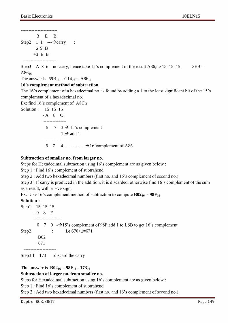
Basic Electronics 10ELN15
Dept. of ECE, SJBIT Page 149
------------------------
3 E B
Step2 1 1 ---carry :
6 9 B
+3 E B
---------------------
Step3 A 8 6 no carry, hence take 15‘s complement of the result A86,i.e 15 15 15- 3EB =
A8616
The answer is 69B16 - C1416= -A8616
16’s complement method of subtraction
The 16‘s complement of a hexadecimal no. is found by adding a 1 to the least significant bit of the 15‘s
complement of a hexadecimal no.
Ex: find 16‘s complement of A8Ch
Solution : 15 15 15
- A 8 C
---------------
5 7 3 15‘s complement
1 add 1
-----------------
5 7 4 -------------16‘complement of A86
Subtraction of smaller no. from larger no.
Steps for Hexadecimal subtraction using 16‘s complement are as given below :
Step 1 : Find 16‘s complement of subtrahend
Step 2 : Add two hexadecimal numbers (first no. and 16‘s complement of second no.)
Step 3 : If carry is produced in the addition, it is discarded, otherwise find 16‘s complement of the sum
as a result, with a –ve sign.
Ex: Use 16‘s complement method of subtraction to compute B0216 - 98F16
Solution :
Step1: 15 15 15
- 9 8 F
-------------------
6 7 0 -15‘s complement of 98F,add 1 to LSB to get 16‘s complement
Step2 : i.e 670+1=671
B02
+671
---------------------
Step3 1 173 discard the carry
The answer is B0216 - 98F16= 17316
Subtraction of larger no. from smaller no.
Steps for Hexadecimal subtraction using 16‘s complement are as given below :
Step 1 : Find 16‘s complement of subtrahend
Step 2 : Add two hexadecimal numbers (first no. and 16‘s complement of second no.)

Basic Electronics 10ELN15
Dept. of ECE, SJBIT Page 150
Step 3 : If carry is produced in the addition, it is discarded, otherwise find 16‘s complement of the sum
as a result, with a –ve sign.
Ex: Use 16‘s complement method of subtraction to compute 38716 - 85416
Solution :
Step1: 15 15 15
8 5 4 -Take15‘s complement of 854,add 1 to LSB to get 16‘s Step2 : --
------------- complement i.e 7AB+1=7AC
Step2
3 8 7
+7 A C
---------------------
Step3 1 B 6 3 no carry, hence take 16‘s complement of B63 and add –ve sign to
it.i.e15 15 15-B63=49C +1=49D
The answer is 16 38716 - 85416=-49D16
Binary Coded Decimal Numbers - BCD
BCD is an abbreviation for binary coded decimal. Bcd is a numeric code in which each digit of a
decimal number is represented by a separate group of bits. The most common BCD code is 8-4-2-1 BCD,
in which each decimal digit is represented by a 4 bit binary number. It is called 8-4-2-1 BCD because
the weights associated from right to left are 1-2-4-8.
The table below shows decimal digit and its corresponding code.
Decimal Number BCD
Number(8421)
0000
1 0001
2 0010
3 0011
4 0100
5 0101
6 0110
7 0111
8 1000
9 1001
In multidigit coding, each decimal digit is individually coded with 8-4-2-1 BCD code
Ex : 58 = 0101 1000
5 8

Basic Electronics 10ELN15
Dept. of ECE, SJBIT Page 151
The advantage of BCD is that it is easy to convert between it and decimal. The disadvantage is the
arithmetic operations are more complex when compared to binary.
BCD ADDITION
The addition of two BCD nos. can be best understood by considering the following three conditions :
Case1: The sum equals 9 or less with no carry
Case2: The sum equals greater than 9 with no carry
Case3: The sum equals 9 or less with a carry
--------------------------------------
Case1: The sum equals 9 or less with no carry
Take two numbers 6 and 3 in BCD and add
6 ----- 0110
3 ----- 0011
---------------------
9 ----- 1001
The addition is carried out as in normal binary addition and the sum is 1001 which is a BCD code for 9.
Case2: The sum equals greater than 9 with no carry
Let us consider addition of the numbers 6 and 8 in BCD
6 ----- 0110
8 ----- 1000
---------------------
14----- 1110 invalid BCD number. This has occurred because the sum of the two
digits exceeds 9. In this case to correct the situation add 6 in BCD i.e 0110 to the invalid
BCD no. as shown below.
6 ----- 0110
8 ----- 1000
---------------------
14----- 1110
0110
-----------------
0001 0100
Observe that after addition of 6 a carry is produced into the second decimal position.
Case3: The sum equals 9 or less with a carry
Let us consider addition of the numbers 8 and 9 in BCD
8 ----- 1000
9 ------1001
---------------------
17 0001 0001 In correct BCD No.
0110 Add 6 for correction
---------------------------
0001 0111 BCD for 17

Basic Electronics 10ELN15
Dept. of ECE, SJBIT Page 152
Going through the above cases we can write the following BCD addition procedure :
BCD Subtraction
A negative BCD no. can be expressed by taking 9‘s complement or 10‘s complement.
The9‘s complement of a decimal number is found by subtracting each digit in the number by 9.The 10‘s
complement is 9‘s complement +1
Decimal Number 9’s complement 10’s
complement
0 9 0
1 8 9
2 7 8
3 6 7
4 5 6
5 4 5
6 3 4
7 2 3
8 1 2
9 0 1
In 9‘s or 10‘s complement subtraction :
Subtraction of smaller no. from larger no.
when 9‘s or 10‘s complement of smaller number is added to the larger no., carry is generated. It is
necessary to add this carry to the result. This is called an end around carry..
Ex : 1
Regular subtraction subtraction in 9‘s subtraction in 10‘s
8 8 8
-2 7 9’s complement of 2 8 10’s complement of 2
--------- ---------- --------
6 1 5 16 –discard the carry
-----1end around carry
------ --------
6 6 Ans
----------------------------------------------------------------------
Ex : 2
Regular subtraction subtraction in 9‘s subtraction in 10‘s

Basic Electronics 10ELN15
Dept. of ECE, SJBIT Page 153
9 9 9
-5 4 9’s complement of 5 5 10’s complement of 5
--------- ---------- --------
4 1 3 1) 4 –discard the carry
--------1 end around carry
------ --------
4 4 Ans
-----------------------------------------------------------------------------------
Subtraction larger no. from smaller no.
When larger no. is subtracted from smaller no.there is no carry, and hence the result is
negative and is in 9‘s complement form, if it is 9‘s complement method of subtraction and is in 10‘s
complement form, if it is 10‘s complement method.
After taking the corresponding complement attach a negative sign to the result to get the answer.
Ex : 1
Regular subtraction subtraction in 9‘s subtraction in 10‘s
2 2 2
-8 9’s complement of 8 2 10’s complement of 2
--------- ---------- --------
-6 3 no carry, hence 4 – no carry, hence take
take 9’s complement of the 10’s complement of the
answer and attach –ve sign answer and attach –ve
i.e 9-3=6, the answer is -6 sign i.e 10-4=6,the ans
wer is –6.
----------------------------------------------------------------------
Ex : 2
Regular subtraction subtraction in 9‘s subtraction in 10‘s
4 4 4
-9 0 9’s complement of 9 1 10’s complement of 9
--------- ---------- --------
- 5 4 no carry, hence 5 no carry, hence take
take 9’s complement of the 10’s complement of the
answer and attach –ve sign answer and attach –ve
i.e 9-4=, the answer is -5 sign i.e 10-5=5,the ans
wer is –5.
From the above examples we can summarize steps for 9‘s and 10‘s complement of BCD subtraction as
follows :
Find the 9‘s or 10‘s complement of a negative no.
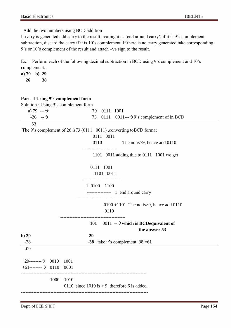
Basic Electronics 10ELN15
Dept. of ECE, SJBIT Page 154
Add the two numbers using BCD addition
If carry is generated add carry to the result treating it as ‗end around carry‘, if it is 9‘s complement
subtraction, discard the carry if it is 10‘s complement. If there is no carry generated take corresponding
9‘s or 10‘s complement of the result and attach –ve sign to the result.
Ex: Perform each of the following decimal subtraction in BCD using 9‘s complement and 10‘s
complement.
a) 79 b) 29
26 38
Part –I Using 9’s complement form
Solution : Using 9‘s complement form
a) 79 --- 79 0111 1001
-26 -- 73 0111 0011---9‘s complement of in BCD
53
The 9‘s complement of 26 is73 (0111 0011) ,converting toBCD format
0111 0011
0110 The no.is>9, hence add 0110
---------------------
1101 0011 adding this to 0111 1001 we get
0111 1001
1101 0011
------------------------
1 0100 1100
---------------- 1 end around carry
----------------------------------
0100 +1101 The no.is>9, hence add 0110
0110
------------------------------------------
101 0011 --which is BCDequivalent of
the answer 53
b) 29 29
-38 -38 take 9‘s complement 38 =61
-09
29-------- 0010 1001
+61-------- 0110 0001
---------------------------------------------------------------------------------
1000 1010
0110 since 1010 is > 9, therefore 6 is added.
----------------------------------------------------------------------------------

Basic Electronics 10ELN15
Dept. of ECE, SJBIT Page 155
1001 0000 ------after addition there is no carry generated, hence
take 9‘s complement of the result
-----------------------------------
0000 1001 ------- 9‘s complement of the result 1001 0000
The answer is –0000 1001 in BCD or –09 in decimal.
Part –II Using 10’s complement form
Solution : Using 10‘s complement form
a) 79 --- 0111 1001
-26 -- 0111 0100------- 10‘s complement of 26 is 74 (i.e 99-26=73+1=74)
53 1110 1101
0110 0110 the result exceeds 9, hence add 6 to the result
1 0101 0011 discard the carry
Hence the answer is 0101 0011 in BCD or 53 in decimal
b) 29 29
-38 -38 take 10‘s complement 38 ( 99-38=61+1=62)
-09
29-------- 0010 1001
+62-------- 0110 0010
---------------------------------------------------------------------------------
1000 1011
0110 since 1010 is > 9, therefore 6 is added.
----------------------------------------------------------------------------------
1001 0001 ------after addition there is no carry generated, hence
take 10‘s complement of the result
-----------------------------------
0000 1001 ------- 10‘s complement of the result
The answer is –0000 1001 in BCD or –09 in decimal.
---------------------------------------- 0 --------------------------------------------------------------

Basic Electronics 10ELN15
Dept. of ECE, SJBIT Page 156
UNIT 8
BOOLEAN ALGEBRA
Symbolic Logic
Boolean algebra derives its name from the mathematician George Boole. Symbolic Logic uses values,
variables and operations
True is represented by the value 1.
False is represented by the value 0.:
Variables are represented by letters and can have one of two values, either 0 or 1. Operations are
functions of one or more variables
AND is represented by X.Y
OR is represented by X + Y
NOT is represented by X' . Throughout this tutorial the X' form will be used and sometime !X
will be used.
These basic operations can be combined to give expressions
Example : X
X.Y
W.X.Y + Z
Precedence
As with any other branch of mathematics, these operators have an order of precedence. NOT operations
have the highest precedence, followed by AND operations, followed by OR operations. Brackets can be
used as with other forms of algebra. e.g.
X.Y + Z and X.(Y + Z) are not the same function
Function Definitions
The logic operations given previously are defined as follows :
Define f(X,Y) to be some function of the variables X and Y.
f(X,Y) = X.Y
f(X,Y) = X.Y
1 if X = 1 and Y = 1
0 Otherwise

Basic Electronics 10ELN15
Dept. of ECE, SJBIT Page 157
f(X,Y) = X + Y
1 if X = 1 or Y = 1
0 Otherwise
f(X) = X'
1 if X = 0
0 Otherwise
Truth Tables
Truth tables are a means of representing the results of a logic function using a table. They are
constructed by defining all possible combinations of the inputs to a function, and then calculating the
output for each combination in turn. For the three functions we have just defined, the truth tables are as
follows
AND
X Y F(X,Y)
0 0 0
0 1 0
1 0 0
1 1 1
OR
X Y F(X,Y)
0 0 0
0 1 1
1 0 1
1 1 1
NOT
X F(X)
0 1
1 0
Truth tables may contain as many input variables as desired

Basic Electronics 10ELN15
Dept. of ECE, SJBIT Page 158
F(X,Y,Z) = X.Y + Z
X Y Z F(X,Y,Z)
0 0 0 0
0 0 1 1
0 1 0 0
0 1 1 1
1 0 0 0
1 0 1 1
1 1 0 1
1 1 1 1
Boolean Switching Algebras
A Boolean Switching Algebra is one which deals only with two-valued variables. Boole's general theory
covers algebras which deal with variables which can hold n values.
Identity :- X + 0 = X, X . 1 = X
Commutative Laws : X + Y = Y + X, X . Y = Y . X
Distributive Laws : X.(Y + Z ) = X.Y + X.Z, X + Y.Z = (X + Y) . (X + Z)
Complement : X + X' = 1, X . X' = 0, The complement X' is unique.
Theorems: A number of theorems may be proved for switching algebras
Idempotent Law : X + X = X, X . X = X
DeMorgan's Law:
(X + Y)' = X' . Y', These can be proved by the use of truth tables.
Proof of (X + Y)' = X' . Y'
X Y X+Y (X+Y)'
0 0 0 1
0 1 1 0
1 0 1 0
1 1 1 0
X Y X' Y' X'.Y'
0 0 1 1 1

Basic Electronics 10ELN15
Dept. of ECE, SJBIT Page 159
0 1 1 0 0
1 0 0 1 0
1 1 0 0 0
The two truth tables are identical, and so the two expressions are identical
(X.Y) = X' + Y', These can be proved by the use of truth tables
Proof of (X.Y) = X' + Y'
X Y X.Y (X.Y)'
0 0 0 1
0 1 0 1
1 0 0 1
X Y X' Y' X'+Y'
0 0 1 1 1
0 1 1 0 1
1 0 0 1 1
1 1 0 0 0
Note : DeMorgans Laws are applicable for any number of variables
Boundedness Law: X + 1 = 1: X . 0 = 0
Absorption Law : X + (X . Y) = X: X . (X + Y ) = X
Elimination Law : X + (X' . Y) = X + Y, X.(X' + Y) = X.Y
Involution theorem : X'' = X
Associative Properties : X + (Y + Z) = (X + Y) + Z, X . ( Y . Z ) = ( X . Y ) . Z
Duality Principle : In Boolean algebras the duality Principle can be obtained by interchanging AND
and OR operators and replacing 0's by 1's and 1's by 0's. Compare the identities on the left side with the
identities on the right.
Example : X.Y+Z' = (X'+Y').Z
It states that for every Boolean expression there exists another expression such that the anding is
replaced by oring,and oring is replaced by anding, and all 0‘s are replaced by 1‘s and all 1‘s are replaced
by 0‘s in the original expression.
Consensus theorem : X.Y + X'.Z + Y.Z = X.Y + X'.Z

Basic Electronics 10ELN15
Dept. of ECE, SJBIT Page 160
or dual form as below, (X + Y).(X' + Z).(Y + Z) = (X + Y).(X' + Z)
Proof of X.Y + X'.Z + Y.Z = X.Y + X'.Z:
X.Y + X'.Z + Y.Z = X.Y + X'.Z
X.Y + X'.Z + (X+X').Y.Z = X.Y + X'.Z
X.Y.(1+Z) + X'.Z.(1+Y) = X.Y + X'.Z
X.Y + X'.Z = X.Y + X'.Z
X.Y'+Z).(X+Y).Z = X.Z+Y.Z instead of X.Z+Y'.Z
X.Y'Z+X.Z+Y.Z
(X.Y'+X+Y).Z
(X+Y).Z
X.Z+Y.Z
The term which is left out is called the consensus term
Given a pair of terms for which a variable appears in one term, and its complement in the other, then the
consensus term is formed by ANDing the original terms together, leaving out the selected variable and
its complement.
The consensus of X.Y and X'.Z is Y.Z
The consensus of X.Y.Z and Y'.Z'.W' is (X.Z).(Z.W')
Summary of Laws And Theorms
Identity Dual
Operations with 0 and 1
X + 0 = X (identity) X.1 = X
X + 1 = 1 (null element) X.0 = 0
Idempotency theorem
X + X = X X.X = X
Complementarity
X + X' = 1 X.X' = 0
Involution theorem
(X')' = X
Cummutative law
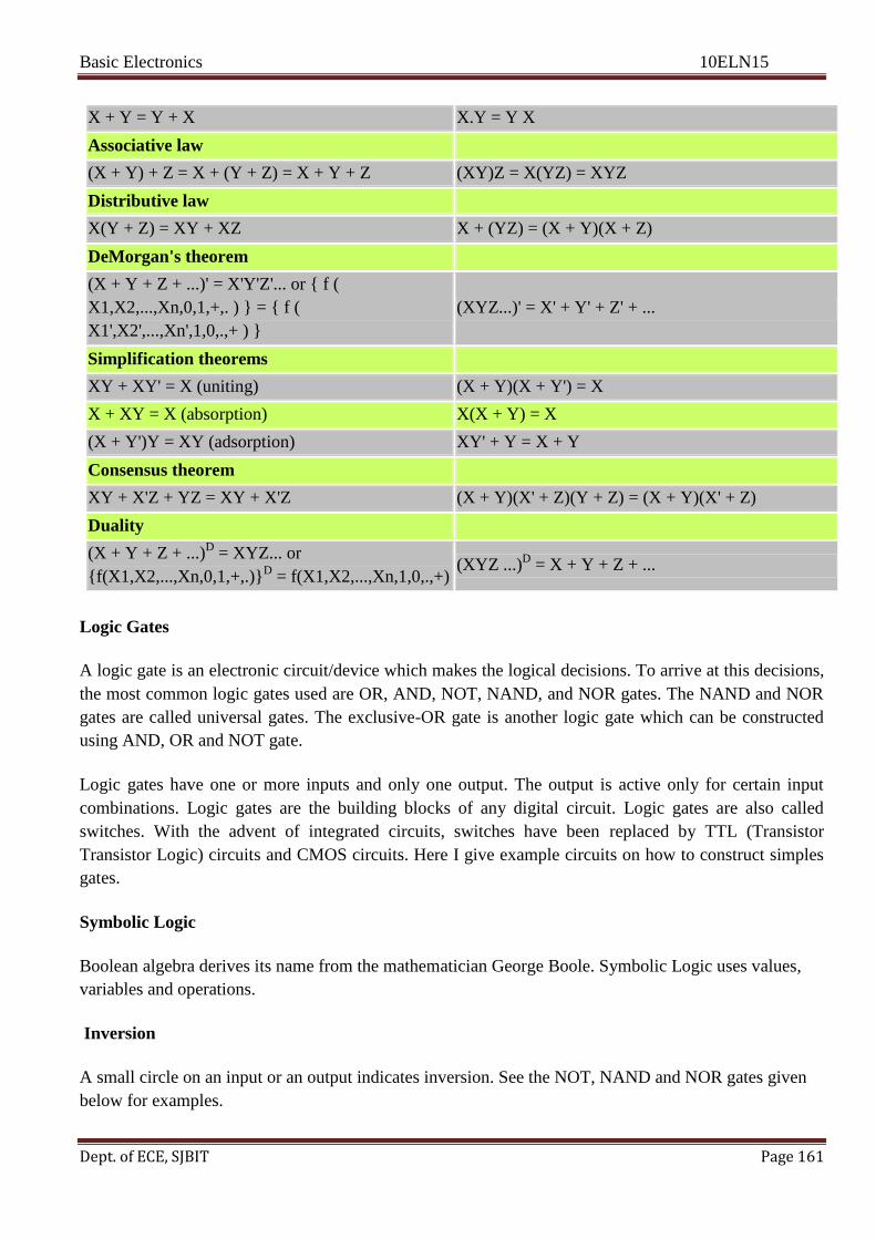
Basic Electronics 10ELN15
Dept. of ECE, SJBIT Page 161
X + Y = Y + X X.Y = Y X
Associative law
(X + Y) + Z = X + (Y + Z) = X + Y + Z (XY)Z = X(YZ) = XYZ
Distributive law
X(Y + Z) = XY + XZ X + (YZ) = (X + Y)(X + Z)
DeMorgan's theorem
(X + Y + Z + ...)' = X'Y'Z'... or f (
X1,X2,...,Xn,0,1,+,. ) = f (
X1',X2',...,Xn',1,0,.,+ )
(XYZ...)' = X' + Y' + Z' + ...
Simplification theorems
XY + XY' = X (uniting) (X + Y)(X + Y') = X
X + XY = X (absorption) X(X + Y) = X
(X + Y')Y = XY (adsorption) XY' + Y = X + Y
Consensus theorem
XY + X'Z + YZ = XY + X'Z (X + Y)(X' + Z)(Y + Z) = (X + Y)(X' + Z)
Duality
(X + Y + Z + ...)D = XYZ... or
f(X1,X2,...,Xn,0,1,+,.)D = f(X1,X2,...,Xn,1,0,.,+)
(XYZ ...)D = X + Y + Z + ...
Logic Gates
A logic gate is an electronic circuit/device which makes the logical decisions. To arrive at this decisions,
the most common logic gates used are OR, AND, NOT, NAND, and NOR gates. The NAND and NOR
gates are called universal gates. The exclusive-OR gate is another logic gate which can be constructed
using AND, OR and NOT gate.
Logic gates have one or more inputs and only one output. The output is active only for certain input
combinations. Logic gates are the building blocks of any digital circuit. Logic gates are also called
switches. With the advent of integrated circuits, switches have been replaced by TTL (Transistor
Transistor Logic) circuits and CMOS circuits. Here I give example circuits on how to construct simples
gates.
Symbolic Logic
Boolean algebra derives its name from the mathematician George Boole. Symbolic Logic uses values,
variables and operations.
Inversion
A small circle on an input or an output indicates inversion. See the NOT, NAND and NOR gates given
below for examples.

Basic Electronics 10ELN15
Dept. of ECE, SJBIT Page 162
Multiple Input Gates
Given commutative and associative laws, many logic gates can be implemented with more than two
inputs, and for reasons of space in circuits, usually multiple input, complex gates are made. You will
encounter such gates in real world (maybe you could analyze an ASIC lib to find this)
Gates Types
AND
OR
NOT
BUF
NAND
NOR
XOR
XNOR
AND Gate
The AND gate performs logical multiplication, commonly known as AND function. The AND gate has
two or more inputs and single output. The output of AND gate is HIGH only when all its inputs are
HIGH (i.e. even if one input is LOW, Output will be LOW).
If X and Y are two inputs, then output F can be represented mathematically as F = X.Y, Here dot (.)
denotes the AND operation. Truth table and symbol of the AND gate is shown in the figure below.
Symbol
Truth Table
X Y F=(X.Y)
0 0 0
0 1 0
1 0 0
1 1 1

Basic Electronics 10ELN15
Dept. of ECE, SJBIT Page 163
Two input AND gate using "diode-resistor" logic is shown in figure below, where X, Y are inputs and F
is the output.
If X = 0 and Y = 0, then both diodes D1 and D2 are forward biased and thus both diodes conduct and
pull F low.
If X = 0 and Y = 1, D2 is reverse biased, thus does not conduct. But D1 is forward biased, thus conducts
and thus pulls F low
If X = 1 and Y = 0, D1 is reverse biased, thus does not conduct. But D2 is forward biased, thus conducts
and thus pulls F low.
If X = 1 and Y = 1, then both diodes D1 and D2 are reverse biased and thus both the diodes are in cut-off
and thus there is no drop in voltage at F. Thus F is HIGH.
Switch Representation of AND Gate
In the figure below, X and Y are two switches which have been connected in series (or just cascaded)
with the load LED and source battery. When both switches are closed, current flows to LED.
OR Gate
The OR gate performs logical addition, commonly known as OR function. The OR gate has two or more
inputs and single output. The output of OR gate is HIGH only when any one of its inputs are HIGH (i.e.
even if one input is HIGH, Output will be HIGH)
If X and Y are two inputs, then output F can be represented mathematically as F = X+Y. Here plus sign
(+) denotes the OR operation. Truth table and symbol of the OR gate is shown in the figure below.

Basic Electronics 10ELN15
Dept. of ECE, SJBIT Page 164
Symbol
Truth Table
X Y F=(X+Y)
0 0 0
0 1 1
1 0 1
1 1 1
Truth Table
Two input OR gate using "diode-resistor" logic is shown in figure below, where X, Y are inputs and F is
the output
Circuit
If X = 0 and Y = 0, then both diodes D1 and D2 are reverse biased and thus both the diodes are in cut-off
and thus F is low
If X = 0 and Y = 1, D1 is reverse biased, thus does not conduct. But D2 is forward biased, thus conducts
and thus pulling F to HIGH.
If X = 1 and Y = 0, D2 is reverse biased, thus does not conduct. But D1 is forward biased, thus conducts
and thus pulling F to HIGH.
If X = 1 and Y = 1, then both diodes D1 and D2 are forward biased and thus both the diodes conduct and
thus F is HIGH.
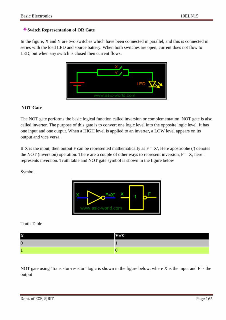
Basic Electronics 10ELN15
Dept. of ECE, SJBIT Page 165
Switch Representation of OR Gate
In the figure, X and Y are two switches which have been connected in parallel, and this is connected in
series with the load LED and source battery. When both switches are open, current does not flow to
LED, but when any switch is closed then current flows.
NOT Gate
The NOT gate performs the basic logical function called inversion or complementation. NOT gate is also
called inverter. The purpose of this gate is to convert one logic level into the opposite logic level. It has
one input and one output. When a HIGH level is applied to an inverter, a LOW level appears on its
output and vice versa.
If X is the input, then output F can be represented mathematically as F = X', Here apostrophe (') denotes
the NOT (inversion) operation. There are a couple of other ways to represent inversion, F= !X, here !
represents inversion. Truth table and NOT gate symbol is shown in the figure below
Symbol
Truth Table
X Y=X'
0 1
1 0
NOT gate using "transistor-resistor" logic is shown in the figure below, where X is the input and F is the
output
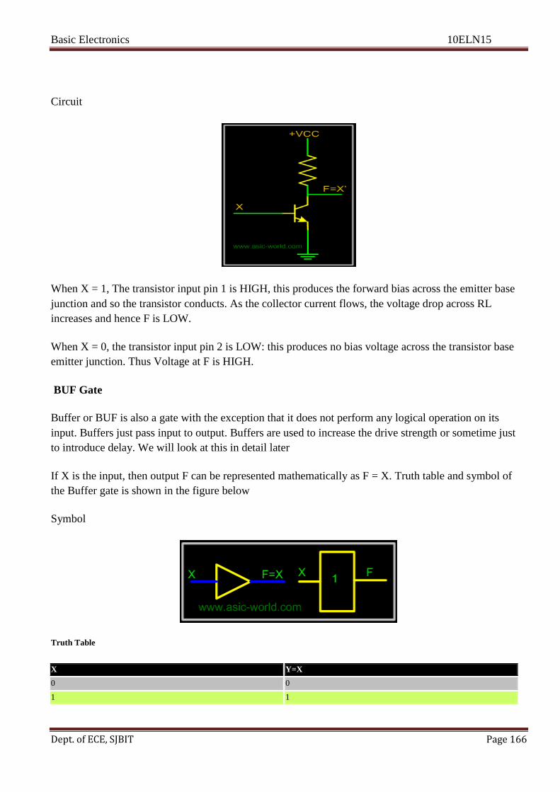
Basic Electronics 10ELN15
Dept. of ECE, SJBIT Page 166
Circuit
When X = 1, The transistor input pin 1 is HIGH, this produces the forward bias across the emitter base
junction and so the transistor conducts. As the collector current flows, the voltage drop across RL
increases and hence F is LOW.
When X = 0, the transistor input pin 2 is LOW: this produces no bias voltage across the transistor base
emitter junction. Thus Voltage at F is HIGH.
BUF Gate
Buffer or BUF is also a gate with the exception that it does not perform any logical operation on its
input. Buffers just pass input to output. Buffers are used to increase the drive strength or sometime just
to introduce delay. We will look at this in detail later
If X is the input, then output F can be represented mathematically as F = X. Truth table and symbol of
the Buffer gate is shown in the figure below
Symbol
Truth Table
X Y=X
0 0
1 1

Basic Electronics 10ELN15
Dept. of ECE, SJBIT Page 167
NAND Gate
NAND gate is a cascade of AND gate and NOT gate, as shown in the figure below. It has two or more
inputs and only one output. The output of NAND gate is HIGH when any one of its input is LOW (i.e.
even if one input is LOW, Output will be HIGH).
NAND From AND and NOT
If X and Y are two inputs, then output F can be represented mathematically as F = (X.Y)', Here dot (.)
denotes the AND operation and (') denotes inversion. Truth table and symbol of the N AND gate is
shown in the figure below. Symbol
Truth Table
X Y F=(X.Y)'
0 0 1
0 1 1
1 0 1
1 1 0
NOR Gate
NOR gate is a cascade of OR gate and NOT gate, as shown in the figure below. It has two or more inputs
and only one output. The output of NOR gate is HIGH when any all its inputs are LOW (i.e. even if one
input is HIGH, output will be LOW)
Symbol
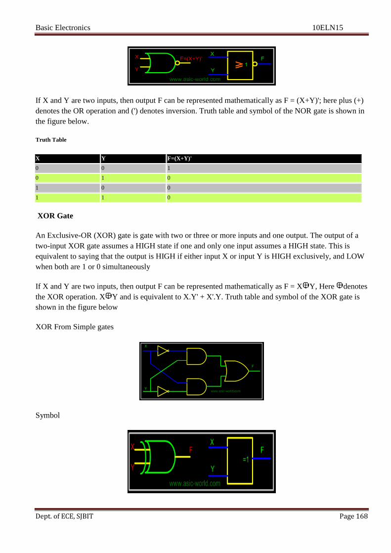
Basic Electronics 10ELN15
Dept. of ECE, SJBIT Page 168
If X and Y are two inputs, then output F can be represented mathematically as F = (X+Y)'; here plus (+)
denotes the OR operation and (') denotes inversion. Truth table and symbol of the NOR gate is shown in
the figure below.
Truth Table
X Y F=(X+Y)'
0 0 1
0 1 0
1 0 0
1 1 0
XOR Gate
An Exclusive-OR (XOR) gate is gate with two or three or more inputs and one output. The output of a
two-input XOR gate assumes a HIGH state if one and only one input assumes a HIGH state. This is
equivalent to saying that the output is HIGH if either input X or input Y is HIGH exclusively, and LOW
when both are 1 or 0 simultaneously
If X and Y are two inputs, then output F can be represented mathematically as F = X Y, Here denotes
the XOR operation. X Y and is equivalent to X.Y' + X'.Y. Truth table and symbol of the XOR gate is
shown in the figure below
XOR From Simple gates
Symbol

Basic Electronics 10ELN15
Dept. of ECE, SJBIT Page 169
Truth Table
X Y F=(X Y)
0 0 0
0 1 1
1 0 1
1 1 0
XNOR Gate
An Exclusive-NOR (XNOR) gate is gate with two or three or more inputs and one output. The output of
a two-input XNOR gate assumes a HIGH state if all the inputs assumes same state. This is equivalent to
saying that the output is HIGH if both input X and input Y is HIGH exclusively or same as input X and
input Y is LOW exclusively, and LOW when both are not same.
f X and Y are two inputs, then output F can be represented mathematically as F = X Y, Here
denotes the XNOR operation. X Y and is equivalent to X.Y + X'.Y'. Truth table and symbol of the
XNOR gate is shown in the figure below.
Symbol
Truth Table
X Y F=(X Y)'
0 0 1
0 1 0
1 0 0
1 1 1
Universal Gates

Basic Electronics 10ELN15
Dept. of ECE, SJBIT Page 170
Universal gates are the ones which can be used for implementing any gate like AND, OR and NOT, or
any combination of these basic gates; NAND and NOR gates are universal gates. But there are some
rules that need to be followed when implementing NAND or NOR based gate
To facilitate the conversion to NAND and NOR logic, we have two new graphic symbols for these gates
NAND Gate
NOR Gate
Realization of logic function using NAND gates
Any logic function can be implemented using NAND gates. To achieve this, first the logic function has
to be written in Sum of Product (SOP) form. Once logic function is converted to SOP, then is very easy
to implement using NAND gate. In other words any logic circuit with AND gates in first level and OR
gates in second level can be converted into a NAND-NAND gate circuit.
Consider the following SOP expression
F = W.X.Y + X.Y.Z + Y.Z.
The above expression can be implemented with three AND gates in first stage and one OR gate in
second stage as shown in figure
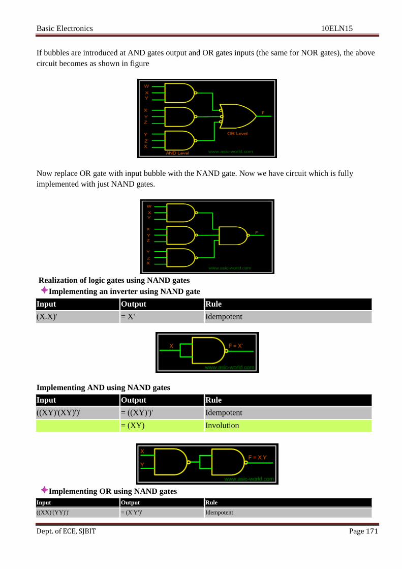
Basic Electronics 10ELN15
Dept. of ECE, SJBIT Page 171
If bubbles are introduced at AND gates output and OR gates inputs (the same for NOR gates), the above
circuit becomes as shown in figure
Now replace OR gate with input bubble with the NAND gate. Now we have circuit which is fully
implemented with just NAND gates.
Realization of logic gates using NAND gates
Implementing an inverter using NAND gate
Input Output Rule
(X.X)' = X' Idempotent
Implementing AND using NAND gates
Input Output Rule
((XY)'(XY)')' = ((XY)')' Idempotent
= (XY) Involution
Implementing OR using NAND gates
Input Output Rule
((XX)'(YY)')' = (X'Y')' Idempotent

Basic Electronics 10ELN15
Dept. of ECE, SJBIT Page 172
= X''+Y'' DeMorgan
= X+Y Involution
Implementing NOR using NAND gates
Input Output Rule
((XX)'(YY)')' =(X'Y')' Idempotent
=X''+Y'' DeMorgan
=X+Y Involution
=(X+Y)' Idempotent
Realization of logic function using NOR gates
Any logic function can be implemented using NOR gates. To achieve this, first the logic function has to
be written in Product of Sum (POS) form. Once it is converted to POS, then it's very easy to implement
using NOR gate. In other words any logic circuit with OR gates in first level and AND gates in second
level can be converted into a NOR-NOR gate circuit.
Consider the following POS expression
F = (X+Y) . (Y+Z)
The above expression can be implemented with three OR gates in first stage and one AND gate in
second stage as shown in figure.
If bubble are introduced at the output of the OR gates and the inputs of AND gate, the above circuit
becomes as shown in figure.

Basic Electronics 10ELN15
Dept. of ECE, SJBIT Page 173
Now replace AND gate with input bubble with the NOR gate. Now we have circuit which is fully
implemented with just NOR gates.
Realization of logic gates using NOR gates
Implementing an inverter using NOR gate
Input Output Rule
(X+X)' = X' Idempotent
Implementing AND using NOR gates
Input Output Rule
((X+X)'+(Y+Y)')' =(X'+Y')' Idempotent
= X''.Y'' DeMorgan
= (X.Y) Involution
Implementing OR using NOR gates
Input Output Rule
((X+Y)'+(X+Y)')' = ((X+Y)')' Idempotent
= X+Y Involution

Basic Electronics 10ELN15
Dept. of ECE, SJBIT Page 174
Implementing NAND using NOR gates
Input Output Rule
((X+Y)'+(X+Y)')' = ((X+Y)')' Idempotent
= X+Y Involution
= (X+Y)' Idempotent
Introduction
Arithmetic circuits are the ones which perform arithmetic operations like addition, subtraction,
multiplication, division, parity calculation. Most of the time, designing these circuits is the same as
designing muxers, encoders and decoders.
In the next few pages we will see few of these circuits in detail.
Adders
Adders are the basic building blocks of all arithmetic circuits; adders add two binary numbers and give
out sum and carry as output. Basically we have two types of adders
Half Adder.
Full Adder.
Half Adder
Adding two single-bit binary values X, Y produces a sum S bit and a carry out C-out bit. This operation
is called half addition and the circuit to realize it is called a half adder

Basic Electronics 10ELN15
Dept. of ECE, SJBIT Page 175
Truth Table
X Y SUM CARRY
0 0 0 0
0 1 1 0
1 0 1 0
1 1 0 1
Symbol
S (X,Y) = (1,2)
S = X'Y + XY'
S = X Y
CARRY(X,Y) = (3)
CARRY = XY
Circuit
Full Adder
Full adder takes a three-bits input. Adding two single-bit binary values X, Y with a carry input bit C-in
produces a sum bit S and a carry out C-out bit.
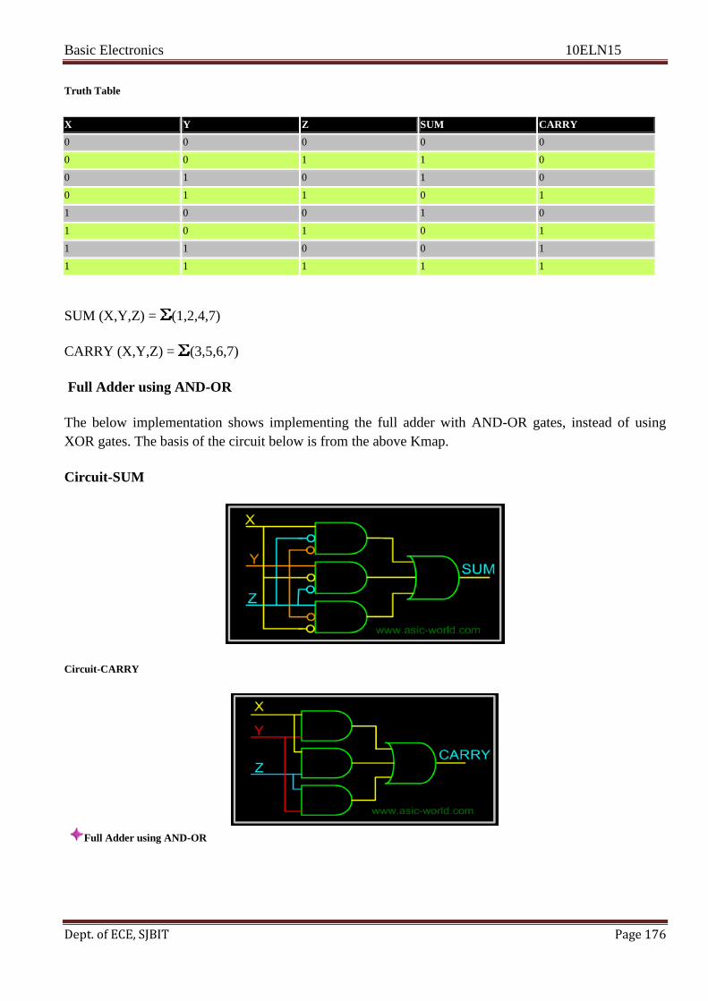
Basic Electronics 10ELN15
Dept. of ECE, SJBIT Page 176
Truth Table
X Y Z SUM CARRY
0 0 0 0 0
0 0 1 1 0
0 1 0 1 0
0 1 1 0 1
1 0 0 1 0
1 0 1 0 1
1 1 0 0 1
1 1 1 1 1
SUM (X,Y,Z) = (1,2,4,7)
CARRY (X,Y,Z) = (3,5,6,7)
Full Adder using AND-OR
The below implementation shows implementing the full adder with AND-OR gates, instead of using
XOR gates. The basis of the circuit below is from the above Kmap.
Circuit-SUM
Circuit-CARRY
Full Adder using AND-OR

Basic Electronics 10ELN15
Dept. of ECE, SJBIT Page 177
Circuit-SUM
Circuit-CARRY
Digital Logic Families.
Logic families can be classified broadly according to the technologies they are built with. In earlier days
we had vast number of these technologies, as you can see in the list below.
DL : Diode Logic.
RTL : Resistor Transistor Logic.
DTL : Diode Transistor Logic.
HTL : High threshold Logic.
TTL : Transistor Transistor Logic.
ECL : Emitter coupled logic.
MOS : Metal Oxide Semiconductor Logic (PMOS and NMOS).
CMOS : Complementary Metal Oxide Semiconductor Logic.
Among these, only CMOS is most widely used by the ASIC (Chip) designers; we will still try to
understand a few of the extinct / less used technologies. More in-depth explanation of CMOS will be
covered in the VLSI section
Basic Concepts
Before we start looking at the how gates are built using various technologies, we need to understand a
few basic concepts. These concepts will go long way i.e. if you become a ASIC designer or Board
designer, you may need to know these concepts very well.
Fan-in.
Fan-out.

Basic Electronics 10ELN15
Dept. of ECE, SJBIT Page 178
Noise Margin.
Power Dissipation.
Gate Delay.
Wire Delay.
Skew.
Voltage Threshold
Fan-in
Fan-in is the number of inputs a gate has, like a two input AND gate has fan-in of two, a three input
NAND gate as a fan-in of three. So a NOT gate always has a fan-in of one. The figure below shows the
effect of fan-in on the delay offered by a gate for a CMOS based gate. Normally delay increases
following a quadratic function of fan-in.
Fan-out
The number of gates that each gate can drive, while providing voltage levels in the guaranteed range, is
called the standard load or fan-out. The fan-out really depends on the amount of electric current a gate
can source or sink while driving other gates. The effects of loading a logic gate output with more than its
rated fan-out has the following effects
In the LOW state the output voltage VOL may increase above VOLmax.
In the HIGH state the output voltage VOH may decrease below VOHmin.
The operating temperature of the device may increase thereby reducing the reliability of the
device and eventually causing the device failure.
Output rise and fall times may increase beyond specifications
The propagation delay may rise above the specified value.
Normally as in the case of fan-in, the delay offered by a gate increases with the increase in fan-out.

Basic Electronics 10ELN15
Dept. of ECE, SJBIT Page 179
Two input OR gate using "diode-resistor" logic is shown in figure below, where X, Y are inputs and F is
the output
Circuit
If X = 0 and Y = 0, then both diodes D1 and D2 are reverse biased and thus both the diodes are in cut-off
and thus F is low
If X = 0 and Y = 1, D1 is reverse biased, thus does not conduct. But D2 is forward biased, thus conducts
and thus pulling F to HIGH.
If X = 1 and Y = 0, D2 is reverse biased, thus does not conduct. But D1 is forward biased, thus conducts
and thus pulling F to HIGH.
If X = 1 and Y = 1, then both diodes D1 and D2 are forward biased and thus both the diodes conduct and
thus F is HIGH
Points to Ponder
Diode Logic suffers from voltage degradation from one stage to the next.
Diode Logic only permits OR and AND functions.
Diode Logic is used extensively but not in integrated circuits.
Resistor Transistor Logic
In RTL (resistor transistor logic), all the logic are implemented using resistors and transistors. One basic
thing about the transistor (NPN), is that HIGH at input causes output to be LOW (i.e. like a inverter).
Below is the example of a few RTL logic circuits.

Basic Electronics 10ELN15
Dept. of ECE, SJBIT Page 180
A basic circuit of an RTL NOR gate consists of two transistors Q1 and Q2, connected as shown in the
figure above. When either input X or Y is driven HIGH, the corresponding transistor goes to saturation
and output Z is pulled to LOW.
Diode Transistor Logic
In DTL (Diode transistor logic), all the logic is implemented using diodes and transistors. A basic circuit
in the DTL logic family is as shown in the figure below. Each input is associated with one diode. The
diodes and the 4.7K resistor form an AND gate. If input X, Y or Z is low, the corresponding diode
conducts current, through the 4.7K resistor flows through the the corresponding diode to ground. Thus
there is no current through the diodes connected in series to transistor base . Hence the transistor does
not conduct, thus remains in cut-off, and output is High.
If all the inputs X, Y, Z are driven high, the diodes in series conduct, driving the transistor into
saturation. Thus output out is Low.
Transistor Transistor Logic
In Transistor Transistor logic or just TTL, logic gates are built only around transistors. TTL was
developed in 1965. Through the years basic TTL has been improved to meet performance requirements.
There are many versions or families of TTL.

Basic Electronics 10ELN15
Dept. of ECE, SJBIT Page 181
Standard TTL.
High Speed TTL
Low Power TTL.
Schhottky TTL.
Here we will discuss only basic TTL as of now; maybe in the future I will add more details about other
TTL versions. As such all TTL families have three configurations for outputs
Totem - Pole output.
Open Collector Output.
Tristate Output.
Before we discuss the output stage let's look at the input stage, which is used with almost all versions of
TTL. This consists of an input transistor and a phase splitter transistor. Input stage consists of a multi
emitter transistor as shown in the figure below. When any input is driven low, the emitter base junction
is forward biased and input transistor conducts. This in turn drives the phase splitter transistor into cut-
off.
Totem - Pole Output
Below is the circuit of a totem-pole NAND gate, which has got three stages
Input Stage
Phase Splitter Stage
Output Stage
Input stage and Phase splitter stage have already been discussed. Output stage is called Totem-Pole
because transistor Q3 sits upon Q4.
Q2 provides complementary voltages for the output transistors Q3 and Q4, which stack one above the
other in such a way that while one of these conducts, the other is in cut-off
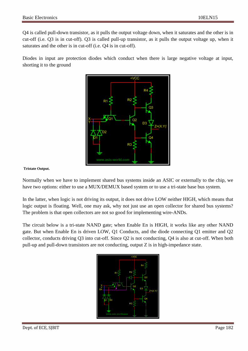
Basic Electronics 10ELN15
Dept. of ECE, SJBIT Page 182
Q4 is called pull-down transistor, as it pulls the output voltage down, when it saturates and the other is in
cut-off (i.e. Q3 is in cut-off). Q3 is called pull-up transistor, as it pulls the output voltage up, when it
saturates and the other is in cut-off (i.e. Q4 is in cut-off).
Diodes in input are protection diodes which conduct when there is large negative voltage at input,
shorting it to the ground
Tristate Output.
Normally when we have to implement shared bus systems inside an ASIC or externally to the chip, we
have two options: either to use a MUX/DEMUX based system or to use a tri-state base bus system.
In the latter, when logic is not driving its output, it does not drive LOW neither HIGH, which means that
logic output is floating. Well, one may ask, why not just use an open collector for shared bus systems?
The problem is that open collectors are not so good for implementing wire-ANDs.
The circuit below is a tri-state NAND gate; when Enable En is HIGH, it works like any other NAND
gate. But when Enable En is driven LOW, Q1 Conducts, and the diode connecting Q1 emitter and Q2
collector, conducts driving Q3 into cut-off. Since Q2 is not conducting, Q4 is also at cut-off. When both
pull-up and pull-down transistors are not conducting, output Z is in high-impedance state.